Sustaining the Si Revolution: From 3D Transistors to 3D Integrationtking/presentations/... ·...
29
Sustaining the Si Revolution: From 3D Transistors to 3D Integration Tsu‐Jae King Liu Department of Electrical Engineering and Computer Sciences University of California, Berkeley, CA USA February 23, 2015 2015 SPIE Advanced Lithography Symposium
Transcript of Sustaining the Si Revolution: From 3D Transistors to 3D Integrationtking/presentations/... ·...
Sustaining the Si Revolution:From 3D Transistors
to 3D Integration
Tsu‐Jae King Liu
Department of Electrical Engineering and Computer Sciences University of California, Berkeley, CA USA
February 23, 2015
2015 SPIE Advanced Lithography Symposium

Impact of Moore’s Law
Source: Morgan Stanley Research
# DEV
ICES
YEAR
1011
1010
109
108
107
106
1960 1970 1980 1990 2000 2010 20302020
MarketGrowth
Investment
TransistorScaling
Lower Cost/ComponentHigher Performance
Mobile Internet
Desktop Internet
PC
Minicomputer
Mainframe
Internet of Things (IoT)Gordon E. Moore
2
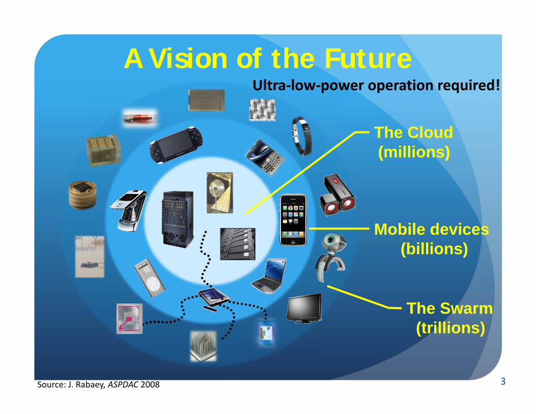
The Cloud(millions)
The Swarm(trillions)
A Vision of the Future
Mobile devices(billions)
Source: J. Rabaey, ASPDAC 2008
Ultra‐low‐power operation required!
3

Data Center Electricity Usage
*J. Koomey, Growth in Data center electricity use 2005 to 2010 (Analytics Press, Oakland, CA), 2011
Google’s Finland data center uses frigid water from the Baltic Sea for cooling.
http://www.wired.com/2012/01/google‐finland/
Data centers accounted for ~1.4% of electricity use worldwide in 2010*
4

Outline
The path to 3D Transistors The CMOS Power Crisis Improving Energy Efficiency
Pathways to 3D Integration
Summary
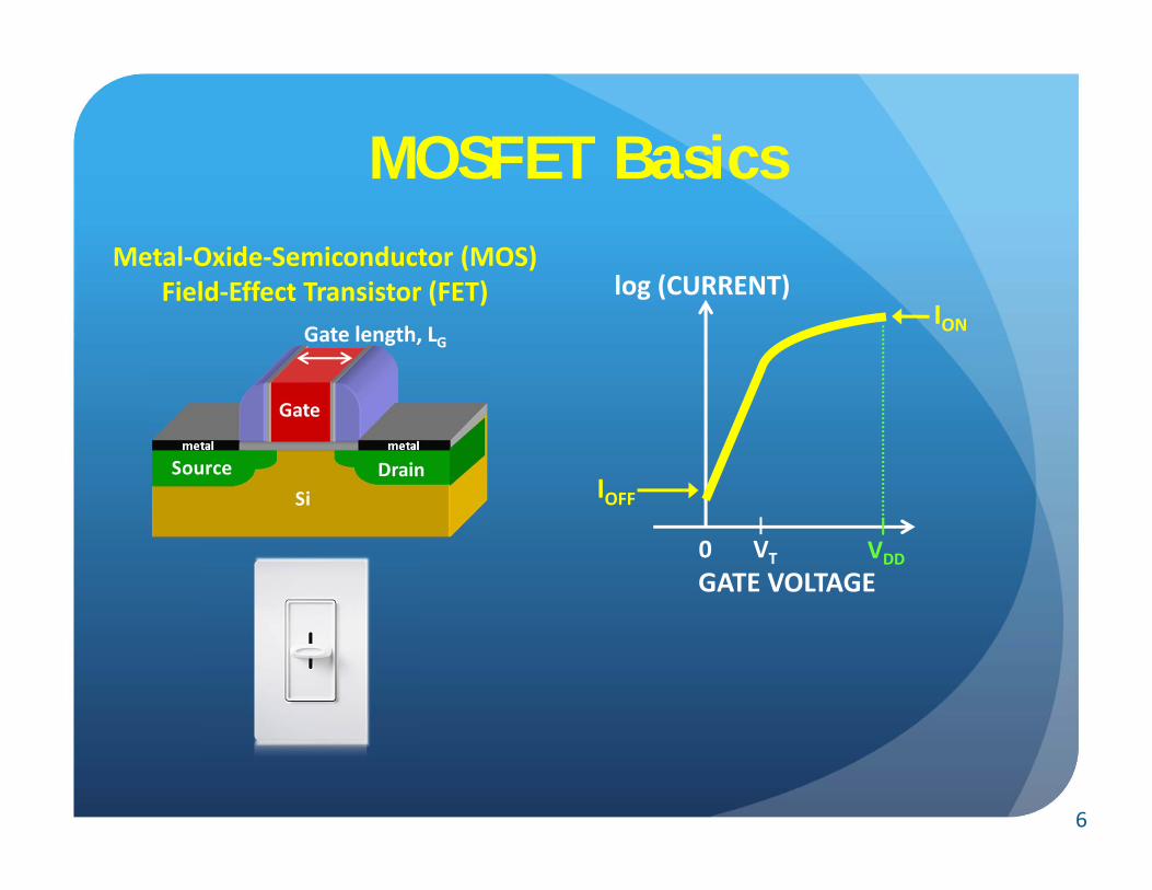
MOSFET Basics
GATE VOLTAGE
log (CURRENT)
0 VT VDD
ION
IOFF
Metal‐Oxide‐Semiconductor (MOS)Field‐Effect Transistor (FET)
Gate length, LG
6

• Voltage scaling has not kept pace with transistor scaling!
Source: P. Packan (Intel), IEDM Short Course, 2007
VDD
6
5
43210
Supp
ly Voltage [V
]
1.4 1.0 .8 .6 .35 .25 .18 .13 .09.065Technology Generation [μm]
VT
Gate Overdrive(VDD‐VT)
10-510-410-310-210-1100101102103
Power Den
sity [W/cm
2 ]
0.01 0.1 1MOSFET Gate Length [μm]
Passive
Active
Source: B. Meyerson (IBM), Semi. Conf., 2005
The CMOS Power Crisis
Technology Node 45 nm 32 nm 22 nm 16/14 nm
Supply voltage, VDD 1.0 V 0.9 V 0.8 V 0.7 V
Power density limits now constrain IC design
7

• Parallelism is the main technique used to improve system performance under a power density constraint.
80858086 286
386486 Pentium®P6
1
10
102
103
104
1970 1980 1990 2000 2010YEAR
POWER
DEN
SIY [W
/cm
2 ] μP Chip Power Density Trend
Source: S. Borkar (Intel)
100
101
102
103
1040
20
40
60
80
100
Normalize
d En
ergy/op
1/throughput [ps/op]
Single coreDual
core
The Advent of Multi-Core Systems
Core 2
Operate at a lower energy point
Run in parallel to recoup performance
8
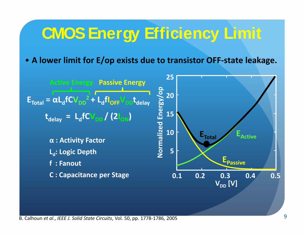
CMOS Energy Efficiency Limit
0.1 0.2 0.3 0.4 0.5
5
10
15
20
25
VDD [V]
Normalize
d En
ergy/op
EActive
EPassive
ETotal
B. Calhoun et al., IEEE J. Solid State Circuits, Vol. 50, pp. 1778‐1786, 2005
ETotal = αLdfCVDD2 + LdfIOFFVDDtdelay
tdelay = LdfCVDD / (2ION)
α : Activity FactorLd: Logic Depth f : FanoutC : Capacitance per Stage
Active Energy Passive Energy
• A lower limit for E/op exists due to transistor OFF‐state leakage.
9

Higher ION/IOFF lower Energy/op
Steeper switching behavior is needed!
log (CURR
ENT)
GATE VOLTAGEEn
ergy
Delay
Improved
Improved
Etotal = LdfCVDD2 [ 1 + (Ldf/2α) / (ION/IOFF) ]
reducing VDD
VDD
VT
1/S
10
Source
DrainGate
LG
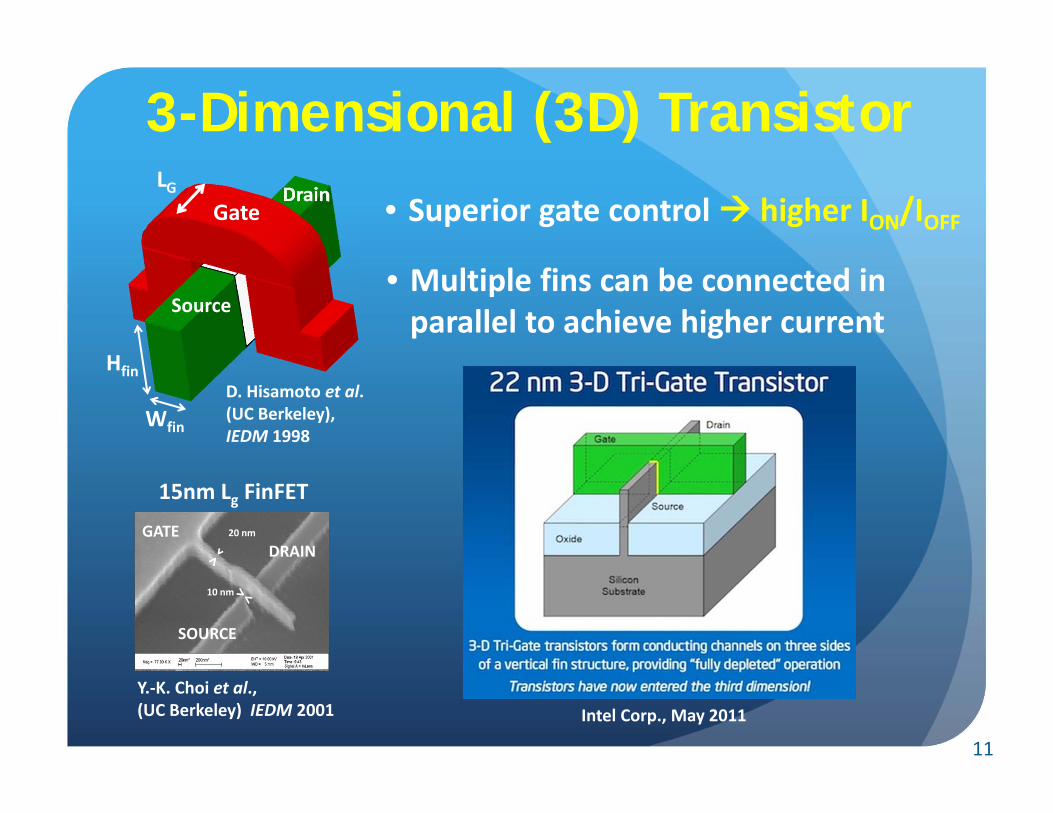
3-Dimensional (3D) Transistor
• Superior gate control higher ION/IOFF
Wfin
Hfin
GATE
SOURCE
DRAIN20 nm
10 nm
Y.‐K. Choi et al., (UC Berkeley) IEDM 2001
15nm Lg FinFET
D. Hisamoto et al. (UC Berkeley), IEDM 1998
Intel Corp., May 2011
• Multiple fins can be connected in parallel to achieve higher current
11
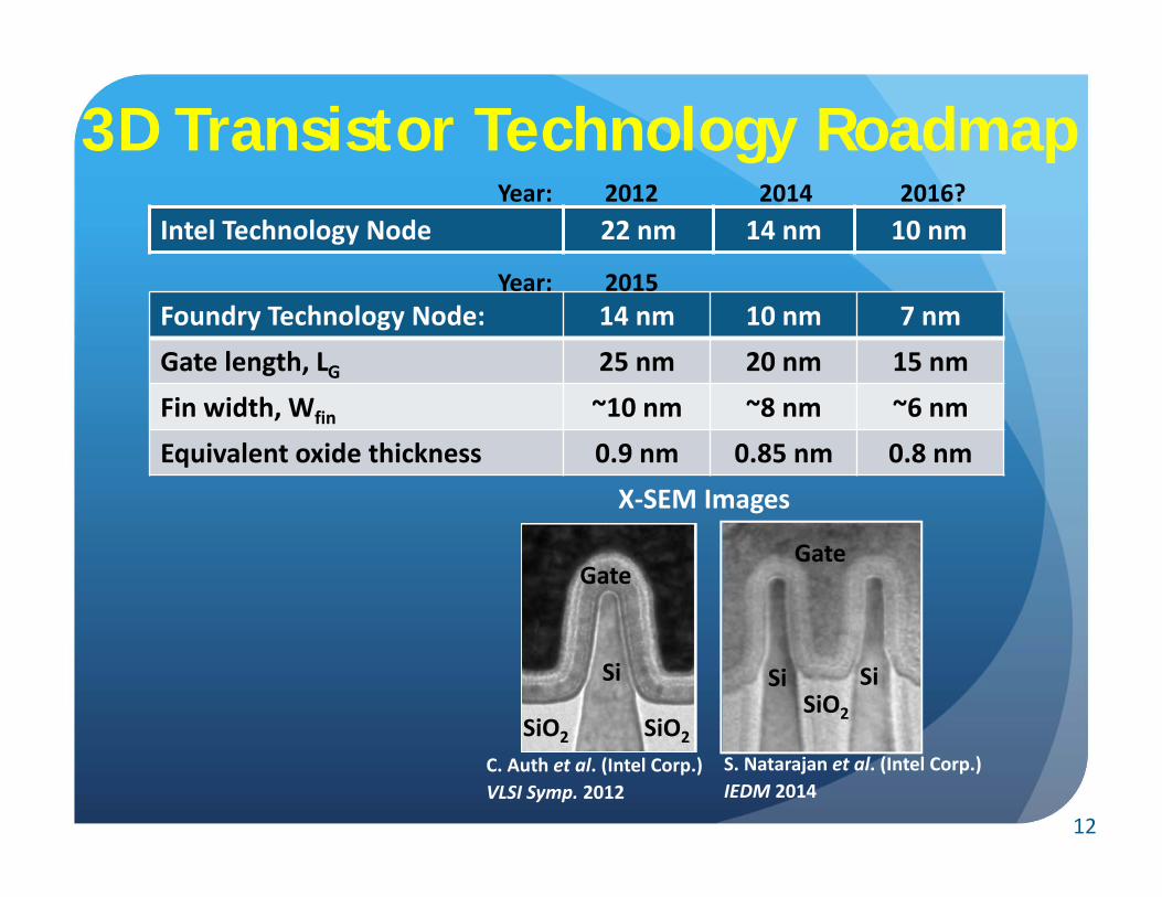
3D Transistor Technology Roadmap
Foundry Technology Node: 14 nm 10 nm 7 nmGate length, LG 25 nm 20 nm 15 nmFin width, Wfin ~10 nm ~8 nm ~6 nmEquivalent oxide thickness 0.9 nm 0.85 nm 0.8 nm
C. Auth et al. (Intel Corp.)VLSI Symp. 2012
X‐SEM Images
Si
SiO2 SiO2
Gate
Intel Technology Node 22 nm 14 nm 10 nm2012 2014 2016?
2015
Gate
Si SiSiO2
S. Natarajan et al. (Intel Corp.)IEDM 2014
Year:
Year:
12

32/28 nmplanar
P. Packan et al. (Intel), IEDM 2009
beyond 10 nmnanowires (NWs)?
C. Dupré et al. (CEA‐LETI)IEDM 2008
Gate‐all‐around FETs must comprise stacked NWs for good area efficiency.
MOSFET Evolution22 nm
thin body
Intel Corp.
FinFET:
FD‐SOI:
K. Cheng et al. (IBM), VLSI Symp. 2011
13
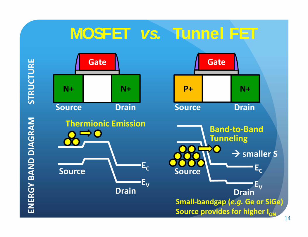
Source Drain
Gate
N+P+
Source
Drain
ECEV
MOSFET vs. Tunnel FET
Source Drain
N+
Gate
N+
Source
Drain
Thermionic Emission
ENER
GY BAN
D DIAGRA
MSTRU
CTURE
ECEV
Band‐to‐BandTunneling
Small‐bandgap (e.g. Ge or SiGe) Source provides for higher ION
smaller S
14
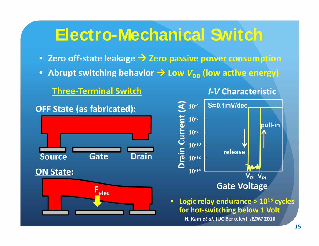
• Zero off‐state leakage Zero passive power consumption
Three‐Terminal Switch I‐V Characteristic
Source DrainGate
ON State:
Felec
OFF State (as fabricated):
Drain Current (A
) S≈0.1mV/dec
VPIVRL
Gate Voltage
10‐4
10‐6
10‐8
10‐10
10‐12
10‐14
pull‐in
release
• Logic relay endurance > 1015 cycles for hot‐switching below 1 VoltH. Kam et al. (UC Berkeley), IEDM 2010
Electro-Mechanical Switch
• Abrupt switching behavior Low VDD (low active energy)
15
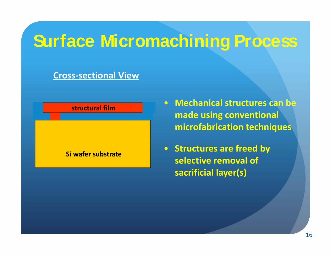
sacrificial layerstructural film
Cross‐sectional View
Si wafer substrate• Structures are freed by
selective removal of sacrificial layer(s)
• Mechanical structures can be made using conventional microfabrication techniques
Surface Micromachining Process
16

4-Terminal Logic Relay
• Voltage applied between the gate and movable body brings the channel into contact with source & drain• Dielectric layer insulates body
Gate
Drain
Source
Gate
Body
A
A’
Isometric View
AA’ Cross‐section
Insulator(Al2O3 )
Body(p+ Si0.4Ge0.6)
Body Dielectric(Al2O3)
channel (W)
Drain (W)Source (W) Gate (W)R. Nathanael et al. (UC Berkeley), IEDM 2009 17
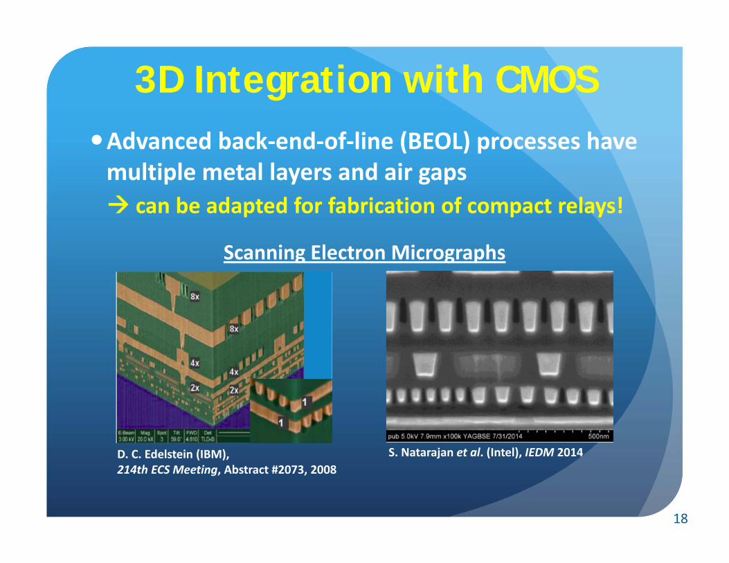
3D Integration with CMOSAdvanced back‐end‐of‐line (BEOL) processes have multiple metal layers and air gaps can be adapted for fabrication of compact relays!
Scanning Electron Micrographs
S. Natarajan et al. (Intel), IEDM 2014D. C. Edelstein (IBM), 214th ECS Meeting, Abstract #2073, 2008
18
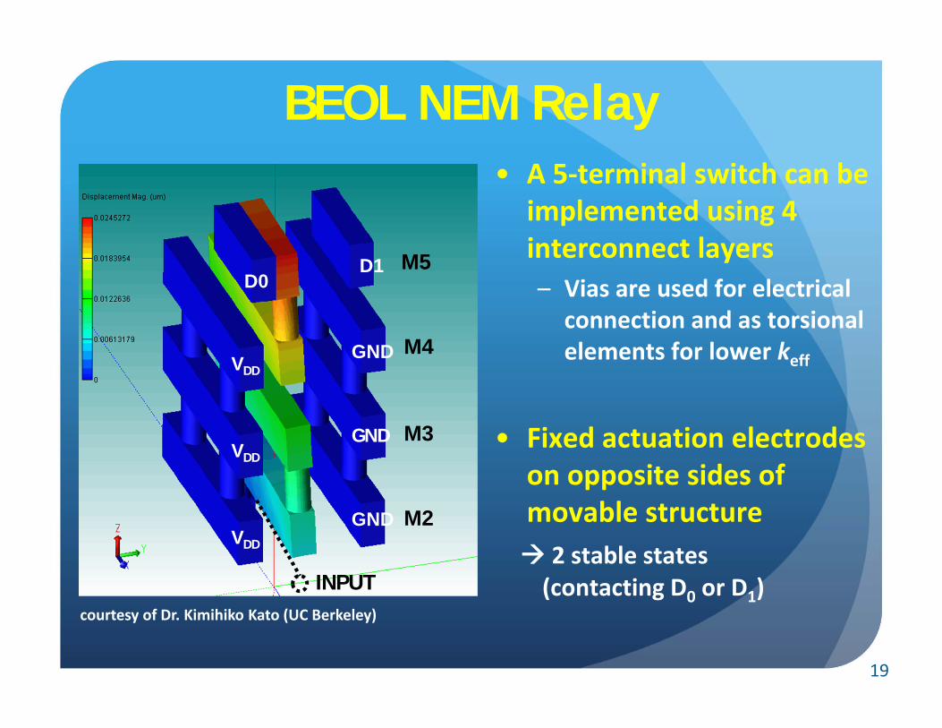
• A 5‐terminal switch can be implemented using 4 interconnect layers– Vias are used for electrical
connection and as torsional elements for lower keff
• Fixed actuation electrodes on opposite sides of movable structure 2 stable states (contacting D0 or D1)
courtesy of Dr. Kimihiko Kato (UC Berkeley)
INPUT
D0D1
VDDGND
VDD
GND
VDD
GND M2
M3
M4
M5
BEOL NEM Relay
19

Outline
The path to 3D Transistors The CMOS Power Crisis Improving Energy Efficiency
Pathways to 3D Integration
Summary

J. J.‐Q. Lu et al., Future Fab International, Issue 23, 2007
3D Packaging
• Enabled by wire bonding and/or flip‐chip bonding
Smaller form factorReduced packaging costReduced power consumption Limited interconnection density
System in Package (SiP), Package on Package (PoP), etc.
Packaging‐based Chip Stack Die‐to‐Wafer Bonding
21

J. J.‐Q. Lu et al., Future Fab International, Issue 23, 2007
3D Transistor Stacking
• Transistor layers can be embedded between interconnect layers
Higher transistor density Heat dissipation Thermal process limitations EDA tool adaptation
Laser‐crystallized Si Polycrystalline Si Bonded Si (on oxide)
22

Moore’s 1965 Paper Revisited
The minimum cost point moves to a larger number of components per IC over time, as manufacturing technology advances (i.e. yield improves).
The primary reason for increasing the number of components per IC was (and still is) lower cost.
*Gordon E. Moore, “Cramming more Components onto Integrated Circuits,” Electronics, pp. 114‐117, April 1965 23

3D NAND Flash Technology
Density scaling is not driven by lithography.Aspect ratios of etched and filled features are very large (>40:1).
Poly‐Si is used as the semiconductor material.
Lithography steps for multiple memory layers are shared.
http://www.monolithic3d.com/uploads/6/0/5/5/6055488/695394.jpg?388 24
J. J.‐Q. Lu et al., Future Fab Int’l, Issue 23, 2007
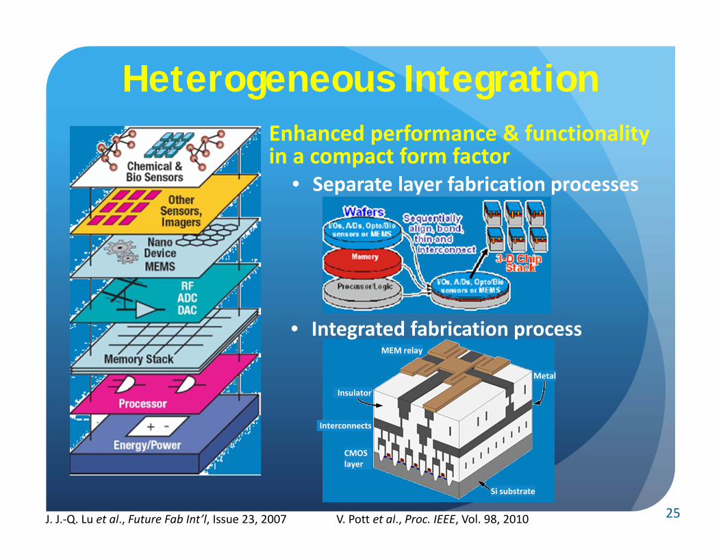
Heterogeneous IntegrationEnhanced performance & functionality in a compact form factor
• Separate layer fabrication processes
MEM relay
Metal
Si substrate
CMOS layer
Interconnects
Insulator
• Integrated fabrication process
25V. Pott et al., Proc. IEEE, Vol. 98, 2010

Texas Instruments Inc.
DMDTM Projection Display Chip
SEM image of pixel array Schematic of 2 pixels
• Electrostatically actuated mirrors built over CMOS circuitry• Structural layers comprise Al alloys; sacrificial material is photoresist
Each mirror corresponds to a single pixel, programmed by an underlying memory cell to deflect light either into a projection lens or light absorber.
< 20 m
26

• Transparent relay fabricated with a CMOS‐compatible process:• SU‐8 photoresist as structural material• Fluorinated photoresist (OSCoR 4000) as dielectric material• SiO2 as sacrificial material
• Can be used as a humidity sensor
Y. Pan et al., 28th IEEE Int’l Conf. MEMS, pp. 940‐943, 2015
Plan‐View SEM
16 20 24 28 3210-14
10-13
10-12
10-11
10-10
10-9
I DS [
A]
VGB [V]
VDR = 32 VVSR = 0 V
RH = 60 %RH = 90 %RH < 10 %
Polymeric RelayMeasured I‐V Characteristics
27
Outline
The path to 3D Transistors The CMOS Power Crisis Improving Energy Efficiency
Pathways to 3D Integration
Summary

Summary 3D transistors and 3D integration provide for improvements in IC energy efficiency and functionality, to sustain the Si revolution.
Market Growth
Investment
Heterogeneous Integration
Transportation
Healthcare
Infrastructure maintenance &disaster response
Energy
Environment
Information technology will be• pervasive• embedded• human‐centered• solving societal‐scale problems
29
Lower Cost/FunctionLower Power


![[Chapter III] Basic Knowledge of Discrete Semiconductor ......transistors (IGBTs) Power transistors (2SAxx,2SBxx,2SCxx,2SDxx, TTAxx,TTBxx,TTCxx,TTDxx) Types of Transistors Transistors](https://static.fdocuments.us/doc/165x107/5e766014341a1a707d5f4c34/chapter-iii-basic-knowledge-of-discrete-semiconductor-transistors-igbts.jpg)