SUPREM-III User’s Manual Version 8628 August 1986 … · Phosphorus Statement ... The default...
186
* SUPREM-III User’s Manual Version 8628 August 1986 Stephen E. Hansen Copyright (C) August 27, 1986 by The Board of Trustees of Stanford University.
Transcript of SUPREM-III User’s Manual Version 8628 August 1986 … · Phosphorus Statement ... The default...

*
SUPREM-III User’s Manual
Version 8628
August 1986
Stephen E. Hansen
Copyright (C) August 27, 1986
by The Board of Trustees of Stanford University.

Suprem-III User´s Manual
1. Table Of Contents-------------------------
Section Page
1. Table Of Contents __________________________________________ 12. Introduction _______________________________________________ 23. The Simulation Structure ___________________________________ 24. Using SUPREM-III ___________________________________________ 25. The SUPREM-III Grid Structure ______________________________ 36. SUPREM-III Output __________________________________________ 47. SUPREM-III Input Statements ________________________________ 48. Manual Format ______________________________________________ 59. Aluminum Statement _________________________________________ 710. Antimony Statement _________________________________________ 911. Arsenic Statement __________________________________________ 1212. Bias Statement _____________________________________________ 1613. Boron Statement ____________________________________________ 1814. Comment Statement __________________________________________ 2115. Deposition Statement _______________________________________ 2216. Diffusion Statement ________________________________________ 2517. DryO2 Statement ____________________________________________ 2818. Electrical Statement _______________________________________ 3219. End.Electrical Statement ___________________________________ 3420. Epitaxy Statement __________________________________________ 3521. Etch Statement _____________________________________________ 3822. Grid Statement _____________________________________________ 3923. Implant Statement __________________________________________ 4024. Impurity Statement _________________________________________ 4225. Initialize Statement _______________________________________ 4726. Loadfile Statement _________________________________________ 5027. Lpplot Statement ___________________________________________ 5128. Material Statement _________________________________________ 5329. Nitride Statement __________________________________________ 5930. Nitrogen Statement _________________________________________ 6131. Oxide Statement ____________________________________________ 6532. Phosphorus Statement _______________________________________ 6733. Plot Statement _____________________________________________ 7234. Polysilicon Statement ______________________________________ 7535. Print Statement ____________________________________________ 8036. Profile Statement __________________________________________ 8437. Resistivity Statement ______________________________________ 8638. Savefile Statement _________________________________________ 8839. Segregation Statement ______________________________________ 8940. Silicon Statement __________________________________________ 9241. Solubility Statement _______________________________________ 9542. Stop Statement _____________________________________________ 9743. Title Statement ____________________________________________ 9844. Vol.Ratio Statement ________________________________________ 9945. V.Threshold Statement ______________________________________ 10146. WetO2 Statement ____________________________________________ 10347. Statement Summary __________________________________________ 10848. Example 1: NMOS Silicon Gate. ______________________________ 11949. Example 2: Bipolar Polysilicon Doped Emitter. ______________ 14750. Suggestions and Bug Reports ________________________________ 171
-1-

Suprem-III User´s Manual
2. Introduction------------------
SUPREM-III is a computer program that allows the user to simulate the various processing steps used inthe manufacture of silicon integrated circuits or discrete devices. The types of processing steps simulated by the cur-rent version of the program are: inert ambient drive-in; oxidation of silicon and silicon-nitride; ion implantation, epi-taxial growth of silicon; and low temperature deposition or etching of various materials. SUPREM-III simulates inone dimension the changes in a semiconductor structure as a result of the various processing steps used in its manu-facture. The primary results of interest are the thicknesses of the various layers of materials that make up the struc-ture and the distribution of impurities within those layers. The program will also determine certain material proper-ties such as polysilicon grain size and the sheet resistivity of diffused regions in silicon layers.
3. The Simulation Structure----------------------------------
In SUPREM-III, a structure whose processing is being simulated is made up of from one to ten layers,each of which is composed of one of ten possible materials. The same material may appear in more than one layer.The default materials defined in SUPREM-III are single crystal silicon, poly-crystalline silicon, silicon dioxide, sili-con nitride, and aluminum. The layers in a structure are numbered sequentially, the bottommost layer being layerone. Diffused regions within a layer are also numbered sequentially with the bottommost region in each layer beingregion one of that layer. A SUPREM-III structure may be doped with up to four impurities, with the default impuri-ties being boron, phosphorus, arsenic, and antimony.
4. Using SUPREM-III---------------------------
To begin a SUPREM-III simulation, all of the coefficients and parameters for the materials and impuritiesmust be input and the initial structure defined. Both of these functions are accomplished by the INITIALIZE state-ment. In its simplest form the initial structure is a single layer of substrate material, though a more complicatedmulti-layer structure generated by a previous simulation may be specified. The coefficients are normally read fromthe default coefficient file and the structure may either be read from a previously saved structure file or definedthrough the parameters of the INITIALIZE statement. In the data file containing the input statements that controlthe SUPREM-III simulation, the INITIALIZE statement must precede all other statements except TITLE, COM-MENT, or STOP statements.
Once the coefficients and the initial structure have been defined, process simulation can begin. If the userwishes to change any of the material or impurity coefficients, new values may be input by using the model parameterstatements. The coefficients defining the impurities are accessed through the impurity statements, BORON, PHOS-PHORUS, ARSENIC, ANTIMONY, and IMPURITY. The material coefficients are accessed through the SILICON,POLYSILICON, OXIDE, NITRIDE, ALUMINUM, and MATERIAL statements. Other coefficients that apply tothe interaction of materials and impurities may be controlled through the SEGREGATION, VOL.RATIO, and MO-BILITY statements. Oxidation rates are controlled by the parameters of the DRYO2, WETO2, and NITROGENstatements. If a user alters any of the coefficients, by using the SAVEFILE statement he may save the modified setof coefficients either into the default coefficient file, S3cof0, creating a new set of defaults, or into an alternate coef-ficient file that can be read in with either the INITIALIZE or the LOADFILE statements.
5. The SUPREM-III Grid Structure-------------------------------------------
In SUPREM-III, the structure is made up of a series of cells. These cells are laid out on a one-dimensionalgrid of points called nodes. Within each layer, each cell is centered about a single node point. The cells at eitherend of a layer are half-cells, with one cell boundary at the endpoint node and the other halfway to the adjacent node
-2-

Suprem-III User´s Manual
within the layer. Within each cell, the physical coefficients and any impurity concentrations are treated as constant.In the current version of the program there may be a maximum of 500 node points or 499 cells or spaces. If an at-tempt is made to use more than the maximum number of node points during a simulation, the program will terminatewith an error.
The distance between adjacent node points within each layer can be controlled by the user, either when alayer is first defined in an INITIALIZE or DEPOSITION statement or at any time in the simulation through theGRID statement. The grid placement is controlled by five parameters; the layer thickness (THICKNESS), the nomi-nal grid spacing (DX), the location of the nominal grid spacing relative to the top surface of the layer (XDX), thenumber of spaces in the layer (SPACES), and the minimum allowed grid spacing (DX.MIN). The way these param-eters are used to control the grid spacing is described below. For the purposes of example, assume that a layer is be-ing deposited on the structure.
In the simplest case the user need only specify the layer’s thickness. In this case the program will assumethat XDX is zero, placing the nominal grid spacing, DX, at the surface of the layer and will use the default DX forthe deposited material. The deposited material, specified by name, has its characteristics, including its default DX,defined by the appropriate material statement. The program will use the number of spaces necessary to achieve auniform grid spacing throughout the layer.
If the default DX is not adequate, then the user may specify both the thickness and the DX, and the pro-gram will work as above except that the specified DX will be used instead of the default value.
In many cases, both to save execution time and to have the structure fit within the limit of 499 grid spaces,a fewer number of spaces may be specified than the program would allocate for uniform grid spacing within the lay-er. In this case a non-uniform grid spacing will be set up within the affected layer. If the number of spaces specifiedis less than the number needed for a uniform grid spacing, the program will place a grid spacing of DX at the loca-tion specified by XDX, and cause the grid spacings to increase parabolically to either side (figure 1). If the numberof spaces specified is greater than the number needed for uniform grid spacings, then the grid spacings will decreasefrom the DX value on either side of XDX (figure 2).
| | | || *| dX2 dX | * |
dX1 |* * | | * * || * * | dX1 |* * |
dX | * | | *| dX2|_____________________| |_____________________|0 XdX thickness 0 XdX thickness
figure 1 figure 2
When a non-uniform grid is set up, the program first determines what the maximum grid spacing would beat either end of the layer assuming a linear variation in grid spacing from XDX, given DX, XDX, the layer thicknessand the number of spaces to use. Then with the nominal DX and the two endpoint grid spacings, the grid is made tovary parabolically from DX to the endpoints in such a way that the resulting grid gives a layer of the specified thick-ness. With this algorithm the user can minimize the number of grid spacings used in the solution and yet place a finemesh where it is needed to accurately represent a rapidly varying impurity distribution.
6. SUPREM-III Output----------------------------
The results of a SUPREM-III simulation are available in both printed and graphic forms. Printed outputcan consist of the following: all material and impurity coefficients as might have been specified by one or more ofthe MATERIAL, IMPURITY, SEGREGATION, or VOL.RATIO statements; information about the current structuresuch as the thicknesses and composition of the various layers, impurity junction depths, or resistivity of layers or dif-fused regions; and the impurity concentrations at each node point and the distance of that point from the structure
-3-

Suprem-III User´s Manual
surface. Plotted or graphic output consists of plots of the specified impurity concentrations versus distance.
7. SUPREM-III Input Statements----------------------------------------
SUPREM-III normally takes its input from a user specified disk file. This file is made up of various state-ments identified by a statement name followed by a parameter list. The statement name is delimited from the pa-rameter list by either a comma and/or one or more blanks. If a comma is present, it may be preceded or followed byany number of blanks. Parameters in a SUPREM-III parameter list are delimited from each other in the same waythe statement name is delimited. If more than one line of input is required for a particular statement, it may be con-tinued on subsequent lines by placing a plus sign as the first non-blank character on the continuation lines.
Parameters in a SUPREM-III parameter list may be one of three types that correspond to the types of val-ues that they may take on. These types are; logical, numerical, and character. Logical parameters take on a value oftrue if the parameter name appears by itself and a value of false if it is preceded by the NOT, (ˆ), character. Numeri-cal type parameters are assigned values in the parameter list by having the parameter name followed by an equalsign and the value. Blanks on either side of the equal sign are ignored. Character parameters may appear in one oftwo ways depending of the statement involved. In one case they hav e a formal parameter name and they are as-signed a character string by use of an equal sign in the same way as a numerical parameter. In the other case thestatement has the character parameter as the only valid parameter and the character string appears by itself followingthe statement name without an associated parameter name.
8. Manual Format----------------------
This manual presents each statement showing the statement name and the associated list of parameters.There are a number of special characters that are used to aid in the description of the parameter lists. These charac-ters are <, >, [, ], (, ), and |.
The <> characters are used to indicate classes of things. For example a parameter description might ap-pear as:
CONCENTRATION=<n>
which indicates that the parameter name is concentration and it is assigned a numerical value. The <n> defines aclass of things represented by n, where n represents the set of numerical values. Valid numerical values are of theform:
9 1.2 -.345 6.7E8 -9.01E-2The only other class defined in this manual is that of character strings represented by <c>.
The [] characters enclose sets of optional items, usually parameters. For example:
STMT1 [ PARM1 ] [ PARM2 PARM3 ] [ PARM4 [ PARM5 ] ]
indicates that on the STMT1 statement, the PARM1 parameter is optional. PARM2 and PARM3 are optional but ifone is specified, both must be specified. PARM4 and PARM5 are optional but PARM5 may be specified only ifPARM4 is specified.
When one or more of a list of items are to be chosen from, they are separated by a | character and enclosedin parenthesis. For example:
STMT2 (PARM1 | PARM2 | (PARM3 PARM4))
-4-

Suprem-III User´s Manual
This indicates that statement STMT2 requires that either PARM1, PARM2, or both PARM3 and PARM4 be speci-fied.
In none of the above examples are the special characters actually typed by the user when inputting aSUPREM-III input sequence.
-5-

Suprem-III User´s Manual
9. Aluminum Statement-----------------------------
The ALUMINUM statement is used to input or modify the characteristics of aluminum as a layer material.
ALUMINUM
[ NAME=<c> ] [ DX.DEFAU=<n> ][ CONDUCTO ][ SPECIES=<n> ] [ DENSITY=<n> ][ AT.WT.1=<n> ] [ AT.NUM.1=<n> ] [ ABUND.1=<n> ][ WORK.FUN=<n> ] [ EPSILONF=<n> ]
Name Type Description---- ---- -----------
ABUND.1 Num The relative abundance of element one in the material. The sum of allabundances for a material must equal one.(unit: )(default: the current value.)(synonym: )
AT .NUM.1 Num The atomic number of element one in the material.(unit: )(default: the current value.)(synonym: )
AT .WT.1 Num The atomic weight of element one in the material.(unit: amu)(default: the current value.)(synonym: )
CONDUCTO Log Specifies that the material is a conductor.(unit: )(default: false.)(synonym: )
DENSITY Num The density of the material.(unit: grams/cmˆ3.)(default: the current value.)(synonym: )
DX.DEFAU Num The default nominal grid spacing for any layer containing this material.(unit: microns.)(default: the current value.)(synonym: )
EPSILONF Num The dielectric constant of the material relative the dielectric constant ofair.(unit: )(default: the current value.)(synonym: )
-6-

Suprem-III User´s Manual
NAME Char The name of the material.(unit: )(default: the current name of the material.)(synonym: )
SPECIES Num The number of different elements in this material.(unit: )(default: the current value.)(synonym: )
WORK.FUN Num The work function of the material.(unit: volts)(default: the current value.)(synonym: )
The ALUMINUM statement is an alias for the MATERIAL statement with an index of five and is used todefine or modify the parameters and coefficients associated with the material aluminum. Not all of the parameters ofthe MATERIAL statement apply to aluminum and so are not listed here.
-7-

Suprem-III User´s Manual
10. Aluminum Statement-------------------------------
The ALUMINUM statement is used to input or modify the characteristics of aluminum as a layer material.
ALUMINUM
[ NAME=<c> ] [ DX.DEFAU=<n> ][ CONDUCTO ][ SPECIES=<n> ] [ DENSITY=<n> ][ AT.WT.1=<n> ] [ AT.NUM.1=<n> ] [ ABUND.1=<n> ][ WORK.FUN=<n> ] [ EPSILONF=<n> ]
Name Type Description---- ---- -----------
ABUND.1 Num The relative abundance of element one in the material. The sum of allabundances for a material must equal one.(unit: )(default: the current value.)(synonym: )
AT .NUM.1 Num The atomic number of element one in the material.(unit: )(default: the current value.)(synonym: )
AT .WT.1 Num The atomic weight of element one in the material.(unit: amu)(default: the current value.)(synonym: )
CONDUCTO Log Specifies that the material is a conductor.(unit: )(default: false.)(synonym: )
DENSITY Num The density of the material.(unit: grams/cmˆ3.)(default: the current value.)(synonym: )
DX.DEFAU Num The default nominal grid spacing for any layer containing this material.(unit: microns.)(default: the current value.)(synonym: )
EPSILONF Num The dielectric constant of the material relative the dielectric constant ofair.(unit: )(default: the current value.)(synonym: )
-8-

Suprem-III User´s Manual
NAME Char The name of the material.(unit: )(default: the current name of the material.)(synonym: )
SPECIES Num The number of different elements in this material.(unit: )(default: the current value.)(synonym: )
WORK.FUN Num The work function of the material.(unit: volts)(default: the current value.)(synonym: )
The ALUMINUM statement is an alias for the MATERIAL statement with an index of five and is used todefine or modify the parameters and coefficients associated with the material aluminum. Not all of the parameters ofthe MATERIAL statement apply to aluminum and so are not listed here.
-9-
Suprem-III User´s Manual
11. Antimony Statement------------------------------
The ANTIMONY statement is used to input or modify the physical or model coefficients associated withantimony as a dopant impurity.
ANTIMONY
[ NAME=<c> ] [ DONOR ][ AT.WT=<n> ] [ AT.NUMB=<n> ][ IONFILE1=<c> ] [ IONFILE2=<c> ][ ( ( SILICON
[ FII.0=<n> ] [ FII.E=<n> ][ K.MF=<n> ] [ K.A=<n> ] [ K.P=<n> ]
)| ( POLYSILI
[ FII.0=<n> ] [ FII.E=<n> ][ ENTROPY=<n> ] [ HEAT.SEG=<n> ] [ Q.SITES=<n> ]
)| ( OXIDE | NITRIDE | ALUMINUM )[ ELECT.ST=<n> ][ DIX.0=<n> ] [ DIX.E=<n> ][ DIM.0=<n> ] [ DIM.E=<n> ][ DIMM.0=<n> ] [ DIMM.E=<n> ]
]
Name Type Description---- ---- -----------
ALUMINUM Log Specifies that the material dependent parameters apply to antimony inaluminum.(unit: )(default: false.)(synonym: )
AT .NUMB Num The atomic number of the impurity.(unit: )(default: the current value.)(synonym: )
AT .WT Num The atomic weight of the impurity.(unit: amu)(default: the current value.)(synonym: )
DIM.0 Num The pre-exponential constant of the diffusion coefficient of the impuritydiffusing with singly negative vacancies.(unit: micronsˆ2/minute.)(default: the current value.)(synonym: )
DIM.E Num The activation energy of the diffusion coefficient of the impurity diffus-ing with singly negative vacancies.(unit: electron volts.)(default: the current value.)(synonym: )
-10-

Suprem-III User´s Manual
DIMM.0 Num The pre-exponential constant of the diffusion coefficient of the impuritydiffusing with doubly negative vacancies.(unit: micronsˆ2/minute.)(default: the current value.)(synonym: )
DIMM.E Num The activation energy of the diffusion coefficient of the impurity diffus-ing with doubly negative vacancies.(unit: electron volts.)(default: the current value.)(synonym: )
DIX.0 Num The pre-exponential constant of the diffusion coefficient of the impuritydiffusing with neutral vacancies.(unit: micronsˆ2/minute.)(default: the current value.)(synonym: )
DIX.E Num The activation energy of the diffusion coefficient of the impurity diffus-ing with neutral vacancies.(unit: electron volts.)(default: the current value.)(synonym: )
DONOR Log Specifies that the impurity is a donor.(unit: )(default: the current value.)(synonym: )
ELECT.ST Num The electric stopping power of the impurity in the specified material.(unit: KeV/micron.)(default: the current value.)(synonym: )
ENTROPY Num The entropy factor. Used to calculate the equilibrium segregation factorat polysilicon grain boundaries.(unit: )(default: the current value.)(synonym: )
FII.0 Num The pre-exponential constant of the fractional partial-interstitialcy contri-bution.(unit: (microns/minute)ˆ(-1/2))(default: the current value.)(synonym: )
FII.E Num The activation energy of the fractional partial-interstitialcy contribution.(unit: electron volts.)(default: the current value.)(synonym: )
HEAT.SEG Num The activation energy of the equilibrium segregation factor at polysilicongrain boundaries.(unit: electron volts.)(default: the current value.)(synonym: )
-11-

Suprem-III User´s Manual
IONFILE1 Char Specifies the primary ion implant range data file for implants using theanalytic distributions. This file will be searched for the range statisticswhen implanting atomic antimony.(unit: )(default: the last file specified.)(synonym: )
IONFILE2 Char Specifies the secondary ion implant range data file for implants using theanalytic distrbutions. This file will be searched for the range statisticswhen implanting the compound ions containing antimony.(unit: )(default: the last file specified.)(synonym: )
K.A Num Used in R. Reif’s epitaxial doping model (see reference in EPITAXYstatement). K.a is a thermodynamic constant relating the dopantspecies concentration in solid silicon and adsorbed layer.(unit: centimeters)(default: the current value.)(synonym: )
K.MF Num Used in R. Reif’s epitaxial doping model (see reference in EPITAXYstatement). K.mf is a kinetic coefficient controlling the rate-limitingstep of the dopant incorporation process.(unit: centimetersˆ(-2) minutesˆ(-1) atmospheresˆ(-1))(default: the current value.)(synonym: )
K.P Num Used in R. Reif’s epitaxial doping model (see reference in EPITAXYstatement). K.p is a thermodynamic constant relating the dopantspecies concentration in solid silicon and gas phase.(unit: centimetersˆ(-3) atmospheresˆ(-1))(default: the current value.)(synonym: )
NAME Char The name of the impurity.(unit: )(default: the last name specified.)(synonym: )
NITRIDE Log Specifies that the material dependent parameters apply to antimony in sil-icon nitride.(unit: )(default: false.)(synonym: )
OXIDE Log Specifies that the material dependent parameters apply to antimony in sil-icon dioxide.(unit: )(default: false.)(synonym: )
POLYSILI Log Specifies that the material dependent parameters apply to antimony inpolysilicon.(unit: )(default: false.)(synonym: )
-12-

Suprem-III User´s Manual
Q.SITES Num Effective density of segregation sites at a grain boundary.(unit: sites/cmˆ2.)(default: the current value.)(synonym: )
SILICON Log Specifies that the material dependent parameters apply to antimony in sil-icon.(unit: )(default: false.)(synonym: )
The ANTIMONY statement is an alias for the IMPURITY statement with an index of four and is used todefine or modify the parameters and coefficients associated with antimony as an impurity. Not all of the parametersof the IMPURITY statement apply to antimony and so are not listed here.
-13-

Suprem-III User´s Manual
12. Arsenic Statement---------------------------
The ARSENIC statement is used to input or modify the physical or model coefficients associated with ar-senic as a dopant impurity.
ARSENIC
[ NAME=<c> ] [ DONOR ][ AT.WT=<n> ] [ AT.NUMB=<n> ][ IONFILE1=<c> ] [ IONFILE2=<c> ][ ( ( SILICON
[ FII.0=<n> ] [ FII.E=<n> ][ K.MF=<n> ] [ K.A=<n> ] [ K.P=<n> ]
[ ( IMPLANT | CHEMICAL )[ CTN.0=<n> ] [ CTN.E=<n> ] [ CTN.F=<n> ]
])
| ( POLYSILI[ ENTROPY=<n> ] [ HEAT.SEG=<n> ] [ Q.SITES=<n> ][ FII.0=<n> ] [ FII.E=<n> ][ ( IMPLANT | CHEMICAL )
[ CTN.0=<n> ] [ CTN.E=<n> ] [ CTN.F=<n> ]]
)| ( OXIDE | NITRIDE | ALUMINUM )[ ELECT.ST=<n> ][ DIX.0=<n> ] [ DIX.E=<n> ][ DIM.0=<n> ] [ DIM.E=<n> ][ DIMM.0=<n> ] [ DIMM.E=<n> ]
]
Name Type Description---- ---- -----------
ALUMINUM Log Specifies that the material dependent parameters apply to arsenic in alu-minum.(unit: )(default: false.)(synonym: )
AT .NUMB Num The atomic number of the impurity.(unit: )(default: the current value.)(synonym: )
AT .WT Num The atomic weight of the impurity.(unit: amu)(default: the current value.)(synonym: )
CHEMICAL Log Specifies that the clustering coefficients apply to the impurity from achemical source.(unit: )(default: false.)(synonym: )
-14-

Suprem-III User´s Manual
CTN.0 Num The pre-exponential constant used in calculating the impurity clusteringcoefficient.(unit: atoms/cmˆ3.)(default: the current value.)(synonym: )
CTN.E Num The activation energy used in calculating the impurity clustering coeffi-cient.(unit: electron volts.)(default: the current value.)(synonym: )
CTN.F Num The power dependence of the concentration used in calculating the impu-rity clustering coefficient.(unit: )(default: the current value.)(synonym: )
DIM.0 Num The pre-exponential constant of the diffusion coefficient of the impuritydiffusing with singly negative vacancies.(unit: micronsˆ2/minute.)(default: the current value.)(synonym: )
DIM.E Num The activation energy of the diffusion coefficient of the impurity diffus-ing with singly negative vacancies.(unit: electron volts.)(default: the current value.)(synonym: )
DIMM.0 Num The pre-exponential constant of the diffusion coefficient of the impuritydiffusing with doubly negative vacancies.(unit: micronsˆ2/minute.)(default: the current value.)(synonym: )
DIMM.E Num The activation energy of the diffusion coefficient of the impurity diffus-ing with doubly negative vacancies.(unit: electron volts.)(default: the current value.)(synonym: )
DIX.0 Num The pre-exponential constant of the diffusion coefficient of the impuritydiffusing with neutral vacancies.(unit: micronsˆ2/minute.)(default: the current value.)(synonym: )
DIX.E Num The activation energy of the diffusion coefficient of the impurity diffus-ing with neutral vacancies.(unit: electron volts.)(default: the current value.)(synonym: )
DONOR Log Specifies that the impurity is a donor in silicon.(unit: )(default: the current value.)(synonym: )
-15-

Suprem-III User´s Manual
ELECT.ST Num The electric stopping power of the impurity in the specified material.(unit: KeV/micron.)(default: the current value.)(synonym: )
ENTROPY Num The entropy factor. Used to calculate the equilibrium segregation factorat polysilicon grain boundaries.(unit: )(default: the current value.)(synonym: )
FII.0 Num The pre-exponential constant of the fractional partial-interstitialcy contri-bution.(unit: (microns/minute)ˆ(-1/2))(default: the current value.)(synonym: )
FII.E Num The activation energy of the fractional partial-interstitialcy contribution.(unit: electron volts.)(default: the current value.)(synonym: )
HEAT.SEG Num The activation energy of the equilibrium segregation factor at polysilicongrain boundaries.(unit: electron volts.)(default: the current value.)(synonym: )
IMPLANT Log Specifies that the impurity clustering coefficients apply to the impurityfrom an implanted source.(unit: )(default: false.)(synonym: )
IONFILE1 Char Specifies the primary ion implant range data file for implants using theanalytic distrbutions. This file will be searched for the range statisticswhen implanting atomic arsenic.(unit: )(default: the last file specified.)(synonym: )
IONFILE2 Char Specifies the secondary ion implant range data file for implants using theanalytic distributions. This file will be searched for the range statisticswhen implanting the compound ions containing arsenic.(unit: )(default: the last file specified.)(synonym: )
K.A Num Used in R. Reif’s epitaxial doping model (see reference in EPITAXYstatement). K.a is a thermodynamic constant relating the dopantspecies concentration in solid silicon and adsorbed layer.(unit: centimeters)(default: the current value.)(synonym: )
-16-
Suprem-III User´s Manual
K.MF Num Used in R. Reif’s epitaxial doping model (see reference in EPITAXYstatement). K.mf is a kinetic coefficient controlling the rate-limitingstep of the dopant incorporation process.(unit: centimetersˆ(-2) minutesˆ(-1) atmospheresˆ(-1))(default: the current value.)(synonym: )
K.P Num Used in R. Reif’s epitaxial doping model (see reference in EPITAXYstatement). K.p is a thermodynamic constant relating the dopantspecies concentration in solid silicon and gas phase.(unit: centimetersˆ(-3) atmospheresˆ(-1))(default: the current value.)(synonym: )
NAME Char The name of the impurity.(unit: )(default: the last name specified.)(synonym: )
NITRIDE Log Specifies that the material dependent parameters apply to arsenic in sili-con nitride.(unit: )(default: false.)(synonym: )
OXIDE Log Specifies that the material dependent parameters apply to arsenic in sili-con dioxide.(unit: )(default: false.)(synonym: )
POLYSILI Log Specifies that the material dependent parameters apply to arsenic inpolysilicon.(unit: )(default: false.)(synonym: )
Q.SITES Num Effective density of segregation sites at a grain boundary.(unit: sites/cmˆ2.)(default: the current value.)(synonym: )
SILICON Log Specifies that the material dependent parameters apply to silicon.(unit: )(default: false.)(synonym: )
The ARSENIC statement is an alias for the IMPURITY statement with an index of three and is used to de-fine or modify the parameters and coefficients associated with arsenic as an impurity. Not all of the parameters ofthe IMPURITY statement apply to arsenic and so are not listed here.
-17-

Suprem-III User´s Manual
13. Bias Statement-----------------------
The BIAS statement is used to specify the bias of conductor and semiconductor layers during a Poissonsolution initiated by the ELECTRICAL statement.
BIAS
LAYER=<n>( [ V.ELECTR=<n> ] [ DV.ELECTR=<n> ] )
| ( ( [ DIFFUSIO=<n> ][ V.MAJORI=<n> ] [ DV.MAJOR=<n> ][ V.MINORI=<n> ] [ DV.MINOR=<n> ]
)| [ FLOAT ]
)
Name Type Description---- ---- -----------
DIFFUSIO Num The index of the diffused region for which the quasi-Fermi potentials arespecified. The parameter is valid only for a semiconductor layer.(unit: )(default: All diffused regions in the layer.)(synonym: )
LAYER Num The index of the conductor or semiconductor layer for which a bias is be-ing specified.(unit: )(default: )(synonym: )
DV.ELECT Num The increment for the bias applied to a conductor layer. This parameteris valid only for a conductor layer.(unit: volts.)(default: 0.0)(synonym: )
DV.MAJOR Num The increment for the quasi-Fermi potential of majority carriers for a dif-fused region of a semiconductor layer. This parameter is valid only fora semiconductor layer.(unit: volts.)(default: 0.0)(synonym: )
DV.MINOR Num The increment for the quasi-Fermi potential of minority carriers for a dif-fused region of a semiconductor layer. This parameter is valid only fora semiconductor layer.(unit: volts.)(default: 0.0)(synonym: )
FLOAT Log Specifies that a polysilicon layer is to be treated as a neutral dielectric.This parameter is valid only for a polysilicon layer.(unit: )(default: false.)
-18-
Suprem-III User´s Manual
(synonym: )
V.ELECTR Num The initial value for the bias applied to a conductor layer. This parameteris valid only for a conductor layer.(unit: volts.)(default: 0.0)(synonym: )
V.MAJORI Num The initial value for the quasi-Fermi potential of majority carriers for adiffused region of a semiconductor layer. This parameter is valid onlyfor a semiconductor layer.(unit: volts.)(default: 0.0)(synonym: )
V.MINORI Num The initial value for the quasi-Fermi potential of minority carriers for adiffused region of a semiconductor layer. This parameter is valid onlyfor a semiconductor layer.(unit: volts.)(default: 0.0)(synonym: )
The BIAS statement specifies the bias of a material layer. One BIAS statement may appear for each con-ductor layer and for each diffused region of a semiconductor layer. Diffused regions are bounded by material inter-faces and metallurgical junctions.
For a semiconductor layer, elimination of the DIFFUSIO parameter applies the specified biases to all dif-fused regions in the layer. Additional BIAS statements may be included to override these values, which are used asthe default values in regions for which specific BIAS statements do not appear.
The increment parameters on the BIAS statement are used to advance the bias values for each Poisson so-lution, where the number of solutions is controlled by the STEPS parameter on the ELECTRICAL statement.
-19-

Suprem-III User´s Manual
14. Boron Statement-------------------------
The BORON statement is used to input or modify the physical or model coefficients associated with boronas a dopant impurity.
BORON
[ NAME=<c> ] [ ACCEPTOR ][ AT.WT=<n> ] [ AT.NUMB=<n> ][ IONFILE1=<c> ] [ IONFILE2=<c> ][ ( ( SILICON
[ FII.0=<n> ] [ FII.E=<n> ][ K.MF=<n> ] [ K.A=<n> ] [ K.P=<n> ]
)| ( POLYSILI
[ ENTROPY=<n> ] [ HEAT.SEG=<n> ] [ Q.SITES=<n> ][ FII.0=<n> ] [ FII.E=<n> ]
)| ( OXIDE | NITRIDE | ALUMINUM )[ ELECT.ST=<n> ][ DIX.0=<n> ] [ DIX.E=<n> ][ DIP.0=<n> ] [ DIP.E=<n> ]
]
Name Type Description---- ---- -----------
ACCEPTOR Log Specifies that the impurity is an acceptor in silicon.(unit: )(default: false.)(synonym: )
ALUMINUM Log Specifies that the material dependent parameters apply to boron in alu-minum.(unit: )(default: false.)(synonym: )
AT .NUMB Num The atomic number of the impurity.(unit: )(default: the current value.)(synonym: )
AT .WT Num The atomic weight of the impurity.(unit: amu)(default: the current value.)(synonym: )
DIP.0 Num The pre-exponential constant of the diffusion coefficient of the impuritydiffusing with positive vacancies.(unit: micronsˆ2/minute.)(default: the current value.)(synonym: )
-20-
Suprem-III User´s Manual
DIP.E Num The activation energy of the diffusion coefficient of the impurity diffus-ing with positive vacancies.(unit: electron volts.)(default: the current value.)(synonym: )
DIX.0 Num The pre-exponential constant of the diffusion coefficient of the impuritydiffusing with neutral vacancies.(unit: micronsˆ2/minute.)(default: the current value.)(synonym: )
DIX.E Num The activation energy of the diffusion coefficient of the impurity diffus-ing with neutral vacancies.(unit: electron volts.)(default: the current value.)(synonym: )
ELECT.ST Num The electric stopping power of the impurity in the specified material.(unit: KeV/micron.)(default: the current value.)(synonym: )
ENTROPY Num The entropy factor. Used to calculate the equilibrium segregation factorat polysilicon grain boundaries.(unit: )(default: the current value.)(synonym: )
FII.0 Num The pre-exponential constant of the fractional partial-interstitialcy contri-bution.(unit: (microns/minute)ˆ(-1/2))(default: the current value.)(synonym: )
FII.E Num The activation energy of the fractional partial-interstitialcy contribution.(unit: electron volts.)(default: the current value.)(synonym: )
HEAT.SEG Num The activation energy of the equilibrium segregation factor at polysilicongrain boundaries.(unit: electron volts.)(default: the current value.)(synonym: )
IONFILE1 Char Specifies the primary ion implant range data file for implants using theanalytic distributions. This file will be searched for the range statisticswhen implanting atomic boron.(unit: )(default: the last file specified.)(synonym: )
IONFILE2 Char Specifies the secondary ion implant range data file for implants using theanalytic distributions. This file will be searched for the range statisticswhen implanting BF2 ions.(unit: )(default: the last file specified.)(synonym: )
-21-

Suprem-III User´s Manual
K.A Num Used in R. Reif’s epitaxial doping model (see reference in EPITAXYstatement). K.a is a thermodynamic constant relating the dopantspecies concentration in solid silicon and adsorbed layer.(unit: centimeters)(default: the current value.)(synonym: )
K.MF Num Used in R. Reif’s epitaxial doping model (see reference in EPITAXYstatement). K.mf is a kinetic coefficient controling the rate-limitingstep of the dopant incorporation process.(unit: centimetersˆ(-2) minutesˆ(-1) atmospheresˆ(-1))(default: the current value.)(synonym: )
K.P Num Used in R. Reif’s epitaxial doping model (see reference in EPITAXYstatement). K.p is a thermodynamic constant relating the dopantspecies concentration in solid silicon and gas phase.(unit: centimetersˆ(-3) atmospheresˆ(-1))(default: the current value.)(synonym: )
NAME Char The name of the impurity.(unit: )(default: the last name specified.)(synonym: )
NITRIDE Log Specifies that the material dependent parameters apply to boron in siliconnitride.(unit: )(default: false.)(synonym: )
OXIDE Log Specifies that the material dependent parameters apply to boron in silicondioxide.(unit: )(default: false.)(synonym: )
POLYSILI Log Specifies that the material dependent parameters apply to boron inpolysilicon.(unit: )(default: false.)(synonym: )
Q.SITES Num Effective density of segregation sites at a grain boundary.(unit: sites/cmˆ2.)(default: the current value.)(synonym: )
SILICON Log Specifies that the material dependent parameters apply to boron in sili-con.(unit: )(default: false.)(synonym: )
The BORON statement is an alias for the IMPURITY statement with an index of one and is used to de-fine or modify the parameters and coefficients associated with boron as an impurity. Not all of the parameters of the
-22-

Suprem-III User´s Manual
IMPURITY statement apply to boron and so are not listed here.
-23-

Suprem-III User´s Manual
15. Comment Statement-----------------------------
The COMMENT statement is used to input a character string to label the following input sequence.
COMMENT [<c>]or
$ [<c>]
The character string associated with the COMMENT statement is output to the standard output device. Ifthe previous statement was neither another COMMENT statement nor a TITLE statement, then a line feed is issuedbefore the character string is output.
-24-

Suprem-III User´s Manual
16. Deposition Statement-------------------------------
The DEPOSITION statement is used to deposit a specified material on top of the current structure. Thematerial may be doped or undoped.
DEPOSITION
THICKNES=<n>( SILICON ( <111> | <110> | <100> )| POLYSILI
TEMPERAT=<n> [ PRESSURE=<n> | GRAINSIZ=<n> ]| OXIDE| NITRIDE| ALUMINUM)[ DX=<n> ] [ XDX=<n> ] [ SPACES=<n> ] [ MIN.DX=<n> ]
[ CONCENTRATION=<n>(ANTIMONY | ARSENIC | BORON | PHOSPHOR)
]
Name Type Description---- ---- -----------
ALUMINUM Log Specifies that the material to be deposited is aluminum.(unit: )(default: false.)(synonym: )
ANTIMONY Log Specifies that the deposited material is to be uniformly doped with anti-mony.(unit: )(default: false.)(synonym: SB)
ARSENIC Log Specifies that the deposited material is to be uniformly doped with ar-senic.(unit: )(default: false.)(synonym: AS)
BORON Log Specifies that the deposited material is to be uniformly doped with boron.(unit: )(default: false.)(synonym: )
CONCENTR Num The concentration at which the deposited material is to be uniformlydoped.(unit: atoms/cmˆ3.)(default: 0.0)(synonym: )
DX Num The nominal grid spacing to be used in the deposited layer at the locationassociated with the XDX parameter.(unit: microns.)(default: the nominal dx of the top layer if its material is the same as is
-25-

Suprem-III User´s Manual
being deposited, otherwise, the default dx of the deposited material.)(synonym: )
GRAINSIZ Num The as-deposited grain size of the deposited polysilicon layer.(unit: microns.)(default: calculated from the deposition temperature and pressure.)(synonym: )
MIN.DX Num The minimum grid spacing that can be used in the layer on which the lay-er is to be deposited.(unit: microns.)(default: the last value specified.)(synonym: )
NITRIDE Log Specifies that the material to be deposited is silicon nitride.(unit: )(default: false.)(synonym: )
OXIDE Log Specifies that the material to be deposited is silicon dioxide.(unit: )(default: false.)(synonym: )
PHOSPHOR Log Specifies that the deposited material is to be uniformly doped with phos-phorus.(unit: )(default: false.)(synonym: )
POLYSILI Log Specifies that the material to be deposited is poly-crystalline silicon.(unit: )(default: false.)(synonym: )
PRESSURE Num The pressure during the deposition of a polysilicon layer.(unit: atmospheres.)(default: 1.0)(synonym: )
SILICON Log Specifies that the material to be deposited is single crystal silicon.(unit: )(default: false.)(synonym: )
SPACES Num The number of spaces to be used in the deposited layer.(unit: )(default: thickness/dx.)(synonym: )
TEMPERAT Num The temperature during deposition of a polysilicon layer.(unit: )(default: degrees Centigrade.)(synonym: )
THICKNES Num The thickness of the deposited layer.(unit: microns.)(default: )(synonym: )
-26-
Suprem-III User´s Manual
XDX Num The distance from the surface of the layer at which the nominal gridspacing, DX, applies.(unit: microns.)(default: 0.)(synonym: )
<100> Log Specifies that the crystalline orientation of the deposited silicon is <100>.(unit: )(default: false.)(synonym: )
<110> Log Specifies that the crystalline orientation of the deposited silicon is <110>.(unit: )(default: false.)(synonym: )
<111> Log Specifies that the crystalline orientation of the deposited silicon is <111>.(unit: )(default: false.)(synonym: )
The DEPOSITION statement is used to deposit a given thickness of the specified material on top of the ex-isting structure. The material deposited may be either undoped or doped uniformly with one of the available impuri-ty types. If the material to be deposited is of the same type as is already present in the top layer of the structure, thenthe material is added to the existing top layer. If the top layer material is of a different type than that being deposit-ed, then a new layer is created for the deposited material.
If single crystal silicon is being deposited, then the crystalline orientation must also be specified. Ifpolysilicon is being deposited, then the deposition temperature must also be specified. The resulting polysilicongrain size will be calculated from the deposition temperature and pressure unless overridden by the user via theGRAINSIZE parameters.
-27-

Suprem-III User´s Manual
17. Diffusion Statement-----------------------------
The DIFFUSION statement is used to model high temperature diffusion in both oxidizing and non-oxidiz-ing ambients.
DIFFUSION
TIME=<n> TEMPERAT=<n> [ T.RATE=<n> ][ ( GAS.CONC=<n> | SOLIDSOL )( ANTIMONY | ARSENIC | BORON | PHOSPHOR )
][ ( DRY O2 | WETO2 | NITROGEN )[ PRESSURE=<n> ] [ P.RATE=<n> ] [ HCL%=<n> ]
][ DTMIN=<n> ] [ DTMAX=<n> ][ ABS.ERR=<n> ] [ REL.ERR=<n> ]
Name Type Description---- ---- -----------
ABS.ERR Num Specifies the maximum desired absolute truncation error. Used to controlthe time step as described below.(unit: centimetersˆ(-3))(default: 1.0E14)(synonym: )
ANTIMONY Log Specifies that the impurity in the ambient gas is antimony.(unit: )(default: false.)(synonym: SB)
ARSENIC Log Specifies that the impurity in the ambient gas is arsenic.(unit: )(default: false.)(synonym: AS)
BORON Log Specifies that the impurity in the ambient gas is boron.(unit: )(default: false.)(synonym: )
DTMAX Num The largest time increment to be used during the solution.(unit: minutes.)(default: 5.0)(synonym: )
DTMIN Num The smallest time increment to be used during the solution.(unit: minutes.)(default: 0.005)(synonym: )
DRYO2 Log Specifies that the ambient gas consists of dry oxygen.(unit: )(default: false.)(synonym: )
-28-

Suprem-III User´s Manual
GAS.CONC Num The concentration of the specified impurity in the ambient gas at the sur-face of the structure.(unit: atoms/cmˆ3.)(default: 0.0)(synonym: CONCENTRATION)
HCL% Num The percentage of chlorine present in the ambient gas.(unit: percent)(default: percentage specified in corresponding ambient statement(DryO2, WetO2, Nitrogen))(synonym: )
NITROGEN Log Specifies that the ambient consists of nitrogen (non-oxidizing ambient).(unit: )(default: true.)(synonym: )
P.RATE Num The rate of change in the ambient gas pressure.(unit: atmospheres/minute.)(default: 0.0)(synonym: )
PHOSPHOR Log Specifies that the impurity in the ambient gas is phosphorus.(unit: false.)(default: )(synonym: )
PRESSURE Num The pressure of the ambient gas. (See note below.)(unit: atmospheres.)(default: pressure specified in corresponding ambient statement(DryO2, WetO2, Nitrogen))(synonym: )
REL.ERR Num Specifies the maximum desired relative truncation error. Used to controlthe time step as described below.(unit: )(default: 0.5)(synonym: )
SOLIDSOL Log Sets the concentration of the specified impurity in the ambient gas at thesurface of the structure to the solid solubility of the impurity in silicon.(unit: )(default: false.)(synonym: )
TIME Num The total elapsed time of the diffusion step being simulated.(unit: minutes.)(default: )(synonym: )
TEMPERAT Num The temperature of the ambient at the beginning of the step.(unit: degrees Centigrade.)(default: )(synonym: )
T.RATE Num The rate of change of the ambient temperature.(unit: degrees Centigrade/minute.)(default: 0.0)(synonym: )
-29-

Suprem-III User´s Manual
WETO2 Log Specifies that the ambient gas consists of wet oxygen or pyrogenic steam.(See note below.)(unit: )(default: false.)(synonym: )
The DIFFUSION statement simulates impurity diffusion in the structure under a variety of oxidizing andnon-oxidizing conditions. At a minimum, only the time and temperature of a step needs to be specified. In this casea non-oxidizing drive-in is assumed. For oxidizing ambients or gaseous predepositions additional parameters needto be specified. The default pressures and chlorine percentages are set previously by the oxidation ambient modelcards (e.g. DRYO2, WETO2, NITROGEN), while the defaults of the other optional parameters are set in the GENIIkey file S3FKY0.
The numerical solution of the diffusion equations requires that the total step time be divided into a numberof smaller time increments, dt’s, in order to insure sufficient accuracy. There are two mechanisms that control thechoice of dt’s, one is due to a restriction on interface movement such that no interface moves more than one cellspacing during a dt. The other time step control algorithm has been chosen to give the desired accuracy without us-ing excessive amounts of computation time. Unless the interface control chooses a smaller dt, it will attempt to usea dt equal to that specified by the DTMIN parameter. Subsequent dt’s are chosen in the following manner.
1. At each point in the current structure a projectedconcentration is calculated from the previous twosolutions.
Cp = C’ + (C’ - C’’)*dt/dt’
Where C’ is the previous concentration, C’’ is theconcentration before that, and dt’ is the previous dt.
2. From the current solution value, C, and the absoluteand relative truncation error parameters, an ‘error’term at each point is then calculated.
Cerr = abs(C - Cp) / (ABS.ERR + abs(C)*REL.ERR)
3. The next dt is then calculated from the followingexpression.
dtnext = dt * sqrt( (1. + dt/dt’)/Cerrmax )
Where Cerrmax is the maximum value of Cerr calculatedat each point in the structure.
4. A value of dtnext is calculated for each impuritypresent with the smallest value being the one thatis ultimately used.
NOTE: The effective oxidant partial pressure for pyrogenic steam reactors has been found to vary significantly fromfacility to facility. It is recommended that the user set the default pressure for WetO2 to a valuethat gives the best agreement with measured oxide thicknesses from his facility.
-30-

Suprem-III User´s Manual
18. DryO2 Statement--------------------------
The DRYO2 statement allows the user to modify the coefficients used to model the oxidation of the vari-ous materials under dry ambient oxidation conditions.
DRYO2
[ ( <111> | <110> | <100> )[ LIN.L.0=<n> ] [ LIN.L.E=<n> ][ LIN.H.0=<n> ] [ LIN.H.E=<n> ][ THINOX.0=<n> ] [ THINOX.E=<n> ] [ THINOX.L=<n> ]
][ PAR.L.0=<n> ] [ PAR.L.E=<n> ][ PAR.H.0=<n> ] [ PAR.H.E=<n> ][ LIN.BREA=<n> ] [ PAR.BREA=<n> ][ LIN.PDEP=<n> ] [ PAR.PDEP=<n> ][ PRESSURE=<n> ] [ HCL%=<n> ][ GAMMA.0=<n> ] [ GAMMA.E=<n> ][ DELTA.0=<n> ] [ DELTA.E=<n> ][ EXP.0=<n> ] [ EXP.E=<n> ][ NIOX.0=<n> ] [ NIOX.E=<n> ] [ NIOX.F=<n> ][ CL.ROW=<n> [ CL.PCT=<n> ]CL.COLUM=<n> [ CL.TEMPE=<n> ][ CL.DEP.L=<n> ] [ CL.DEP.P=<n> ]
]
Name Type Description---- ---- -----------
CL.COLUM Num The column number in the table of coefficients used to calculate the chlo-rine dependence of the oxidation rates.(unit: )(default: the current value.)(synonym: )
CL.DEP.L Num The coefficient modifying the linear oxidation rate in the presence ofchlorine at the specified row and column.(unit: )(default: the current value.)(synonym: )
CL.DEP.P Num The coefficient modifying the parabolic oxidation rate in the presence ofchlorine at the specified row and column.(unit: )(default: the current value.)(synonym: )
CL.PCT Num The percentage of chlorine for which the coefficients in the specified roware valid.(unit: percent.)(default: the current value.)(synonym: )
-31-

Suprem-III User´s Manual
CL.ROW Num The row number in the table of coefficients used to calculate the chlorinedependence of the oxidation rates.(unit: )(default: the current value.)(synonym: )
CL.TEMPE Num The temperature for which the coefficients in the specified column arevalid.(unit: degrees Centigrade.)(default: the current value.)(synonym: )
DELTA.0 Num The pre-exponential factor of the delta coefficient used in calculating theimpurity concentration dependence of the parabolic oxidation rate.(unit: cmˆ3/atom.)(default: the current value.)(synonym: )
DELTA.E Num The activation energy of the delta coefficient used in calculating the im-purity concentration dependence of the parabolic oxidation rate.(unit: electron volts.)(default: the current value.)(synonym: )
EXP.0 Num The pre-exponential factor of the exponent used in calculating the impu-rity concentration dependence of the parabolic oxidation rate.(unit: )(default: the current value.)(synonym: )
EXP.E Num The activation energy of the exponent used in calculating the impurityconcentration dependence of the parabolic oxidation rate.(unit: electron volts.)(default: the current value.)(synonym: )
GAMMA.0 Num The pre-exponential factor of the gamma coefficient used in calculatingthe impurity concentration dependence of the linear oxidation rate.(unit: )(default: the current value.)(synonym: )
GAMMA.E Num The activation energy of the gamma coefficient used in calculating theimpurity concentration dependence of the linear oxidation rate.(unit: electron volts.)(default: the current value.)(synonym: )
HCL% Num The default percentage of chlorine present in the ambient.(unit: percent.)(default: the current value.)(synonym: )
LIN.BREA Num The temperature at which the temperature dependence of the linear oxi-dation rate changes.(unit: degrees Centigrade.)(default: the current value.)(synonym: )
-32-

Suprem-III User´s Manual
LIN.H.0 Num The pre-exponential constant of the linear oxidation rate for temperaturesabove the breakpoint set by L.BREAKP.(unit: microns/minute.)(default: the current value.)(synonym: )
LIN.H.E Num The activation energy of the linear oxidation rate for temperatures abovethe breakpoint set by L.BREAKP.(unit: electron volts.)(default: the current value.)(synonym: )
LIN.L.0 Num The pre-exponential constant of the linear oxidation rate for temperaturesbelow the breakpoint set by L.BREAKP.(unit: microns/minute.)(default: the current value.)(synonym: )
LIN.L.E Num The activation energy of the linear oxidation rate for temperatures belowthe breakpoint set by L.BREAKP.(unit: electron volts.)(default: the current value.)(synonym: )
LIN.PDEP Num The pressure dependence factor for the linear oxidation rate.(unit: )(default: the current value.)(synonym: )
NIOX.0 Num The pre-exponential constant used to determine the oxidation rate of sili-con nitride.(unit: microns.)(default: the current value.)(synonym: )
NIOX.E Num The activation energy used to determine the oxidation rate of silicon ni-tride.(unit: electron volts.)(default: the current value.)(synonym: )
NIOX.F Num The exponent factor used to determine the oxidation rate of silicon ni-tride.(unit: )(default: the current value.)(synonym: )
PAR.BREA Num The temperature at which the temperature dependence of the parabolicoxidation rate changes.(unit: degrees Centigrade.)(default: the current value.)(synonym: )
PAR.H.0 Num The pre-exponential constant of the parabolic oxidation rate for tempera-tures above the breakpoint set by P.BREAKP.(unit: micronsˆ2/minute.)(default: the current value.)(synonym: )
-33-
Suprem-III User´s Manual
PAR.H.E Num The activation energy of the parabolic oxidation rate for temperaturesabove the breakpoint set by P.BREAKP.(unit: electron volts.)(default: the current value.)(synonym: )
PAR.L.0 Num The pre-exponential constant of the parabolic oxidation rate for tempera-tures below the breakpoint set by P.BREAKP.(unit: micronsˆ2/minute.)(default: the current value.)(synonym: )
PAR.L.E Num The activation energy of the parabolic oxidation rate for temperatures be-low the breakpoint set by P.BREAKP.(unit: electron volts.)(default: the current value.)(synonym: )
PAR.PDEP Num The pressure dependence factor for the parabolic oxidation rate.(unit: )(default: the current value.)(synonym: )
PRESSURE Num The default ambient pressure.(unit: atmospheres.)(default: the current value.)(synonym: )
THINOX.0 Num The pre-exponential constant of the thin oxide growth rate parameter.(unit: microns/minute.)(default: the current value.)(synonym: )
THINOX.E Num The activation energy of the thin oxide growth rate parameter.(unit: electron volts.)(default: the current value.)(synonym: )
THINOX.L Num The characteristic length of the thin oxide growth rate parameter.(unit: microns.)(default: the current value.)(synonym: )
<100> Log Specifies that the linear growth rate and thin oxide growth rate parame-ters apply to <100> orientation silicon.(unit: )(default: false.)(synonym: )
<110> Log Specifies that the linear growth rate and thin oxide growth rate parame-ters apply to <110> orientation silicon.(unit: )(default: false.)(synonym: )
<111> Log Specifies that the linear growth rate and thin oxide growth rate parame-ters apply to <111> orientation silicon.(unit: )(default: false.)
-34-
Suprem-III User´s Manual
(synonym: )
The three oxidation model statements, DRYO2, WETO2, and NITROGEN, use identical parameters, dif-fering only in the values assigned. The parameters NIOX.C, NIOX.E, and NIOX.F are used in modeling the oxida-tion of silicon nitride while the others deal with the oxidation of single and polycrystalline silicon.
The effects of chlorine in the ambient gas on the oxidation rate of silicon are currently modeled by an em-pirical expression whose only variable is defined by the L.CLDEP and P.CLDEP for the linear and parabolic ratesrespectively. To date no convenient function is available to calculate the chlorine dependence as a function of tem-perature and amount of chlorine present, therefor a table of values defines the chlorine dependence factors at thosetemperatures and percentages for which reliable data is available. For those temperatures and chlorine percentagesbetween the values in the table, linear interpolation is employed to calculate the value used. For temperatures or per-centages outside the range of values present in the table, the values whose conditions most nearly match the currentconditions are used. For example, if the current conditions are a temperature of 1175 degrees with three percentchlorine, but the highest temperature entry in the table is 1150 degrees and the nearest chlorine percentages are fortwo and four percent, then a value halfway between the values at 1150 degrees and two and four percent chlorinewill be used.
-35-

Suprem-III User´s Manual
19. Electrical Statement-----------------------------
The ELECTRICAL statement begins a series of numerical solutions of Poisson’s equation for the currentstructure.
ELECTRICAL
[ STEPS=<n> ] [ EXTENT=<n> ] [ TEMPERAT=<n> ][ ERROR=<n> ] [ MAX.ITER=<n> ] [ FILE.OUT=<c> ]
Name Type Description---- ---- -----------
ERROR Num The allowed relative error between successive approximations during theiterative solution of Poisson’s equation.(unit: )(default: 1 x 10ˆ-4.)(synonym: )
EXTENT Num The distance by which the bottom layer of the structure is extended forthe numerical solution of Poisson’s equation. This extension is neces-sary to allow for the proper treatment of depletion regions which extendbeyond the bottom of the simulated structure.(unit: microns.)(default: 0.0)(synonym: )
FILE.OUT char The name of the file to which the results of the electrical calculations areto be output. The total hole and electron concentrations and their re-spective conductivities and resistivities are normally written to the stan-dard output, but if a file is specified, they are also written to that file.The potential, net active impurity concentration and the distance fromthe surface at each node are also written to the file.(unit: )(default: )(synonym: )
MAX.ITER Num The maximum number of iterations allowed for each solution of Pois-son’s equation.(unit: )(default: 50)(synonym: )
STEPS Num The number of bias steps for which Poisson’s equation is solved.(unit: )(default: 1)(synonym: )
TEMPERAT Num The device temperature used during the solutions of Poisson’s equation.(unit: degrees Centigrade.)(default: 26.84)(synonym: )
-36-

Suprem-III User´s Manual
The ELECTRICAL statement performs the number of solutions of Poisson’s equation specified by theSTEPS parameter for the current physical structure. The solution region can be extended below the structure usedfor process simulation by using the EXTEND parameter. For a structure having an insulator layer at the top or bot-tom, reflection symmetry is used as the boundary condition at the associated external boundary.
Insulator layers in the structure are treated as charge-neutral dielectrics. Conductor layers are treated asregions having constant specified bias. Semiconductor layers have constant specified quasi-Fermi potentials forelectrons and holes within each diffused region. Polysilicon layers can also be treated as charge-neutral dielectriclayers. The above bias information is specified through a series of BIAS statements which follow the ELECTRI-CAL statement and are terminated by an END.ELECTRICAL statement.
For each Poisson solution, the total electron and hole concentrations, conductivities, and sheet resistancesare calculated and printed for all diffused regions in the semiconductor layers.
-37-

Suprem-III User´s Manual
20. End.Electrical Statement-----------------------------------
The END.ELEC statement terminates a sequence of BIAS statements associated with the ELECTRICstatement.
END.ELEC [ <c> ]
-38-
Suprem-III User´s Manual
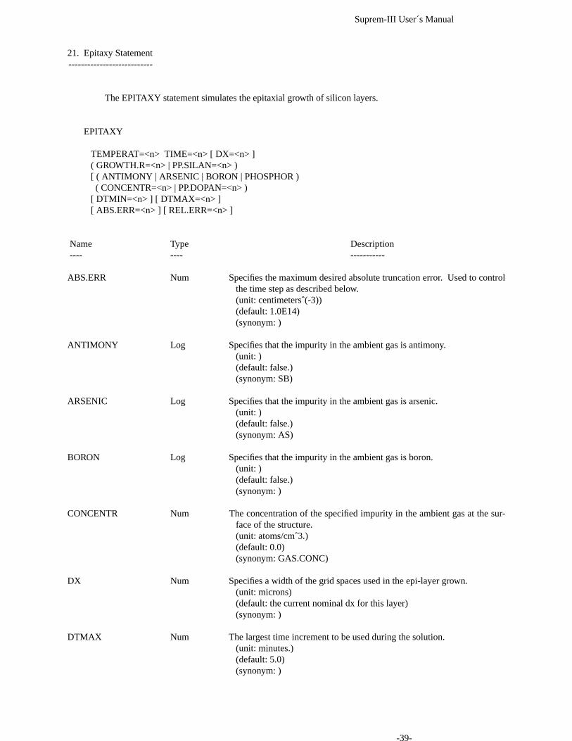
21. Epitaxy Statement---------------------------
The EPITAXY statement simulates the epitaxial growth of silicon layers.
EPITAXY
TEMPERAT=<n> TIME=<n> [ DX=<n> ]( GRO WTH.R=<n> | PP.SILAN=<n> )[ ( ANTIMONY | ARSENIC | BORON | PHOSPHOR )( CONCENTR=<n> | PP.DOPAN=<n> )
[ DTMIN=<n> ] [ DTMAX=<n> ][ ABS.ERR=<n> ] [ REL.ERR=<n> ]
Name Type Description---- ---- -----------
ABS.ERR Num Specifies the maximum desired absolute truncation error. Used to controlthe time step as described below.(unit: centimetersˆ(-3))(default: 1.0E14)(synonym: )
ANTIMONY Log Specifies that the impurity in the ambient gas is antimony.(unit: )(default: false.)(synonym: SB)
ARSENIC Log Specifies that the impurity in the ambient gas is arsenic.(unit: )(default: false.)(synonym: AS)
BORON Log Specifies that the impurity in the ambient gas is boron.(unit: )(default: false.)(synonym: )
CONCENTR Num The concentration of the specified impurity in the ambient gas at the sur-face of the structure.(unit: atoms/cmˆ3.)(default: 0.0)(synonym: GAS.CONC)
DX Num Specifies a width of the grid spaces used in the epi-layer grown.(unit: microns)(default: the current nominal dx for this layer)(synonym: )
DTMAX Num The largest time increment to be used during the solution.(unit: minutes.)(default: 5.0)(synonym: )
-39-

Suprem-III User´s Manual
DTMIN Num The smallest time increment to be used during the solution.(unit: minutes.)(default: 0.005)(synonym: )
GROWTH.R Num The growth rate of the epitaxial layer.(unit: microns/minute.)(default: )(synonym: )
PHOSPHOR Log Specifies that the impurity in the ambient gas is phosphorus.(unit: )(default: false.)(synonym: )
PP.DOPAN Num Specifies the input dopant partial pressure. This is approximately equalto the dopant input flow rate divided by the hydrogen carrier input flowrate. See the R. Reif reference below.(unit: atmospheres)(default: 0.0)(synonym: )
PP.SILAN Num Specifies the input silane partial pressure. This is approximately equal tothe silane input flow rate divided by the hydrogen carrier input flowrate. See the R. Reif reference below.(unit: atmospheres)(default: 0.0)(synonym: )
REL.ERR Num Specifies the maximum desired relative truncation error. Used to controlthe time step as described below.(unit: )(default: 0.5)(synonym: )
TEMPERAT Num The temperature at the beginning of the step.(unit: degrees Centigrade.)(default: )(synonym: )
TIME Num The total elapsed time of the epitaxy step being simulated.(unit: minutes.)(default: )(synonym: )
The EPITAXY statement is used to grow a layer of single crystal silicon on top of the current structure.The epitaxial layer may be either doped or undoped. To grow an epitaxial layer, the top layer must be single crystalsilicon.
The growth rate used in the simulation may be specified in one of two ways. The first is to explicitly spec-ify it with the GROWTH.R parameter. The second is to specify the input partial pressure of silane with thePP.SILAN parameter causing the rate to be determined from the product of the partial pressure and the mass trans-port coefficient of silane in hydrogen as specified by the SILICON statement. (Reference, ‘Computer Simulation inSilicon Epitaxy’, by R. Reif and R. W. Dutton, J. Electrochem. Soc., Vol. 128, No. 4, April 1981, pp 909-918.)
Analogous to the growth rate, the impurity concentration in doped epi-layers may be specified in one oftwo ways. The first is to explicitly specify the surface concentration with the CONCENTR parameter. The second
-40-

Suprem-III User´s Manual
is to specify the input partial pressure of the dopant with the PP.DOPAN parameter. The surface concentration isthen calculated as a function of the partial pressure, time increment, growth rate, and the mass transport and kineticcoefficients, K.a, K.p, and K.mf as specified by the SILICON statement. (See the previous reference.)
The numerical solution of the diffusion equations requires that the total step time be divided into a numberof smaller time increments, dt’s, in order to insure sufficient accuracy. There are two mechanisms that control thechoice of dt’s, one is due to a restriction on interface movement such that no interface moves more than one cellspacing during a dt. The other time step control algorithm has been chosen to give the desired accuracy without us-ing excessive amounts of computation time. Unless the interface control chooses a smaller dt, it will attempt to usea dt equal to that specified by the DTMIN parameter. Subsequent dt’s are chosen in the following manner.
1. At each point in the current structure a projectedconcentration is calculated from the previous twosolutions.
Cp = C’ + (C’ - C’’)*dt/dt’
Where C’ is the previous concentration, C’’ is theconcentration before that, and dt’ is the previous dt.
2. From the current solution value, C, and the absoluteand relative truncation error parameters, an ‘error’term at each point is then calculated.
Cerr = abs(C - Cp) / (ABS.ERR + abs(C)*REL.ERR)
3. The next dt is then calculated from the followingexpression.
dtnext = dt * sqrt( (1. + dt/dt’)/Cerrmax )
Where Cerrmax is the maximum value of Cerr calculatedat each point in the structure.
4. A value of dtnext is calculated for each impuritypresent with the smallest value being the one thatis ultimately used.
-41-

Suprem-III User´s Manual
22. Etch Statement-----------------------
The ETCH statement is used to etch a specified material from the top of the current structure.
ETCH
( SILICON | POLYSILI | OXIDE | NITRIDE | ALUMINUM )[ ( THICKNES=<n> | ALL ) ]
Name Type Description---- ---- -----------
ALL Log Specifies that all of the specified material is to be etched.(unit: )(default: true.)(synonym: )
ALUMINUM Log Specifies that the material to be etched is aluminum.(unit: )(default: false.)(synonym: )
NITRIDE Log Specifies that the material to be etched is silicon nitride.(unit: )(default: false.)(synonym: )
OXIDE Log Specifies that the material to be etched is silicon dioxide.(unit: )(default: false.)(synonym: )
POLYSILI Log Specifies that the material to be etched is poly-crystalline silicon.(unit: )(default: false.)(synonym: )
SILICON Log Specifies that the material to be etched is single crystal silicon.(unit: )(default: false.)(synonym: )
THICKNESS Num The amount of the material to be etched.(unit: microns.)(default: the surface layer thickness.)(synonym: AMOUNT)
The ETCH statement is used to etch a specified amount of the specified material from the top of the exist-ing structure. If the material at the top of the structure is not the material specified then no etching takes place. Ifthe amount to be etched is not specified then the entire layer is removed.
-42-

Suprem-III User´s Manual
23. Grid Statement-----------------------
The GRID statement specifies the grid spacing parameters for one or more of the layers in a structure. Forthe first layer, the thickness may also be extended.
GRID
LAYER.<n> [ THICKNES=<n> ] [ DX=<n> ] [ MIN.DX=<n> ][ XDX=<n> ] [ SPA CES=<n> ]
Name Type Description---- ---- -----------
DX Num The nominal grid spacing in to be used in the specified layer(s) at the lo-cation associated with the XDX parameter.(unit: microns.)(default: The current nominal grid spacing.)(synonym: )
LAYER.<n> Log Specifies that the grid parameters are to apply to the n’th layer of thestructure.(unit: )(default: false.)(synonym: )
MIN.DX Num The minimum grid spacing that can be used in the specified layer(s).(unit: microns.)(default: The current minimum grid spacing.)(synonym: )
SPACES Num The number of spaces to be used in the specified layer(s).(unit: )(default: The current number of spaces in the layer.)(synonym: )
THICKNESS Num The thickness of the first layer. If the specified thickness is greater thanthe current layer thickness, then additional material is added to the bot-tom of the layer. The value specified must be greater than or equal tothe current thickness.(unit: microns.)(default: The current layer thickness.)(synonym: )
XDX Num The distance from the surface of the layer at which the nominal gridspacing, DX, applies.(unit: microns.)(default: The last value specified.)(synonym: )
The GRID statement is used primarily to change the grid spacing of one or more layers of the currentstructure. In the case of the first, or bottom layer, the GRID statement may be used to extend the depth of the layerby adding additional material to the bottom of the structure. In this case, the impurity concentration at the bottom-most cell in the structure is used uniformly in the added region.
-43-

Suprem-III User´s Manual
24. Implant Statement---------------------------
The IMPLANT statement is used to simulate the ion-implantation of impurities into the structure. Fourtypes of implantation models are available, a numerical method based on the Boltzman transport equation, and threeanalytical methods based on simple Gaussian, two sided Gaussian, or Pearson type-IV distributions.
IMPLANT
DOSE=<n> ENERGY=<n>( ANTIMONY | ARSENIC | BF2 | BORON | PHOSPHOR )( GAUSSIAN| 2-GAUSSI| PEARSON| ( BOLTZMAN [ MINSTEPS=<n> ] [ AT.WT=<n> ] [ AT.NUMB=<n> ] ))
Name Type Description---- ---- -----------
ANTIMONY Log Specifies that the ion to be implanted is antimony.(unit: )(default: false.)(synonym: SB)
ARSENIC Log Specifies that the ion to be implanted is arsenic.(unit: )(default: false.)(synonym: AS)
AT .NUMB Num The atomic number of the ion to be implanted.(unit: )(default: The last value specified in the corresponding impurity coeffi-cient statement)(synonym: )
AT .WT Num The atomic weight of the ion to be implanted.(unit: amu)(default: The last value specified in the corresponding impurity coeffi-cient statement)(synonym: AT.MASS)
BF2 Log Specifies that the ion to be implanted is boron-difluoride.(unit: )(default: false.)(synonym: )
BOLTZMAN Log Specifies that the Boltzman transport model is to be used in simulatingthe implantation.(unit: )(default: false.)(synonym: )
-44-

Suprem-III User´s Manual
BORON Log Specifies that the ion to be implanted is atomic boron.(unit: )(default: false.)(synonym: )
DOSE Num The implanted dose.(unit: atoms/cmˆ2.)(default: )(synonym: )
ENERGY Num The energy of the implant beam.(unit: thousand electron volts.)(default: )(synonym: )
GAUSSIAN Log Specifies that a simple Gaussian distribution is to be used to model theimplanted profile.(unit: )(default: false.)(synonym: )
MINSTEPS Num The minimum number of steps between each grid point used in calculat-ing the energy distribution during the solution of the Boltzman trans-port equation.(unit: )(default: 5.0)(synonym: )
PEARSON Log Specifies that a Pearson type-IV distribution is to be used to model theimplanted profile.(unit: )(default: true, if no other model is specified.)(synonym: )
PHOSPHOR Log Specifies that the ion to be implanted is phosphorus.(unit: )(default: false.)(synonym: )
2-GAUSSI Log Specifies that a two sided Gaussian distribution is to be used to model theimplanted profile.(unit: )(default: false.)(synonym: )
The IMPLANT statement is used to simulate ion-implantation of impurities into the structure. Four differ-ent ion-implantation models are available.
When the BOLTZMANN option is selected, the implanted ion distribution is calculated by a numerical so-lution of the Boltzmann transport equation [1]. In this method, the momentum distribution of the implanted ion isdetermined at each depth in the target. Then distribution in energy and angle is represented numerically by a two-di-mensional array (default size 15 x 8).
The calculation proceeds starting from the surface, where the momentum distribution is known to be adelta function (mono-energetic beam moving normal to the target surface). A knowledge of the scattering cross sec-tion for both two-body atomic and electronic interactions, together with the transport equations, is then sufficient todetermine how the momentum distribution evolves with depth. Material discontinuities are simple to handle, since
-45-

Suprem-III User´s Manual
only the cross sections change as the ions cross any interface. When any ion scatters to an energy less than about5% of the initial energy, or when an ion is scattered back toward the target surface, that ion is considered stopped atthat depth and becomes part of the range distribution. The calculation proceeds until the concentration of the im-planted profile drops to 10ˆ-5 of its peak value.
The other three models are based on fitting the as-implanted distribution to an analytical function. Thethree functions available are a simple Gaussian, a two sided Gaussian, or a Pearson type-IV distribution. The neces-sary moments, or range statistics, are read from the implant moment data file specified via the appropriate impuritysstatement.
-46-
Suprem-III User´s Manual
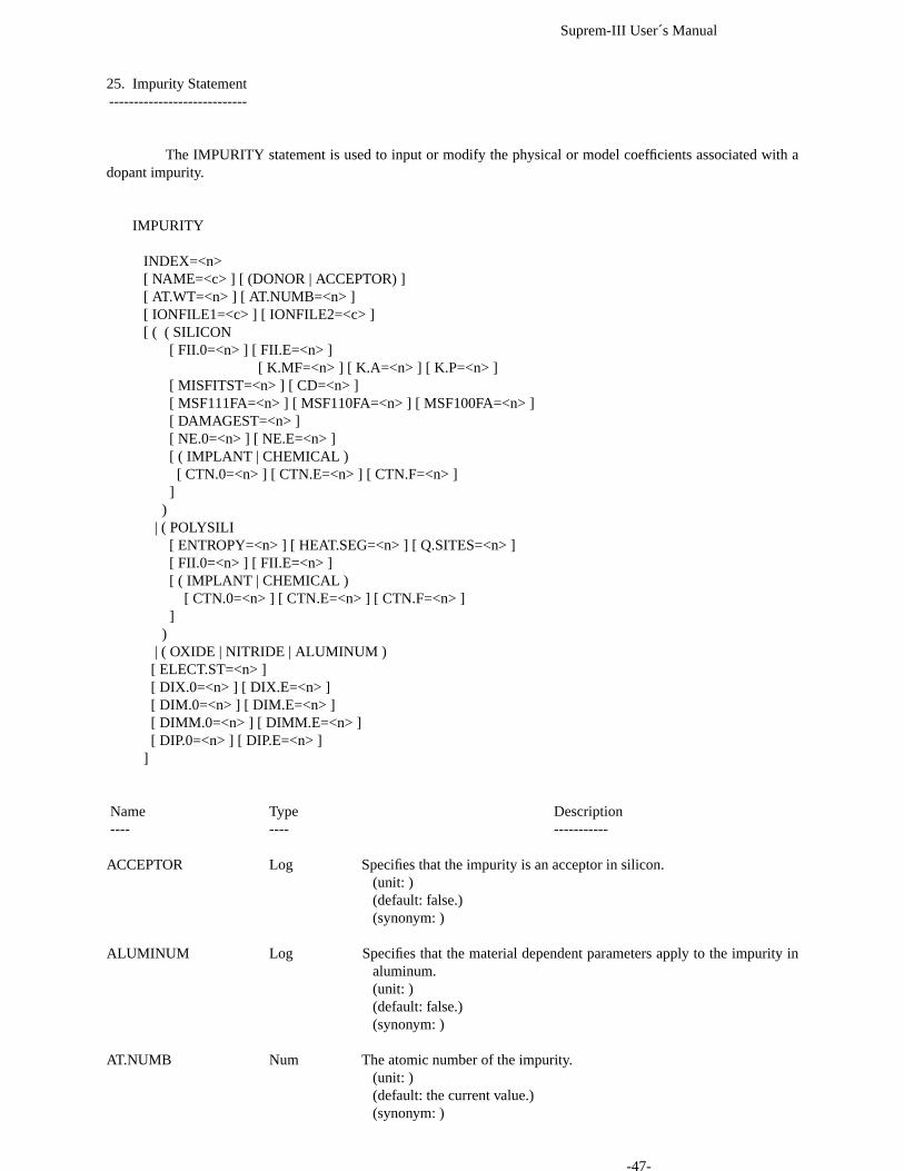
25. Impurity Statement----------------------------
The IMPURITY statement is used to input or modify the physical or model coefficients associated with adopant impurity.
IMPURITY
INDEX=<n>[ NAME=<c> ] [ (DONOR | ACCEPTOR) ][ AT.WT=<n> ] [ AT.NUMB=<n> ][ IONFILE1=<c> ] [ IONFILE2=<c> ][ ( ( SILICON
[ FII.0=<n> ] [ FII.E=<n> ][ K.MF=<n> ] [ K.A=<n> ] [ K.P=<n> ]
[ MISFITST=<n> ] [ CD=<n> ][ MSF111FA=<n> ] [ MSF110FA=<n> ] [ MSF100FA=<n> ][ DAMAGEST=<n> ][ NE.0=<n> ] [ NE.E=<n> ][ ( IMPLANT | CHEMICAL )[ CTN.0=<n> ] [ CTN.E=<n> ] [ CTN.F=<n> ]
])
| ( POLYSILI[ ENTROPY=<n> ] [ HEAT.SEG=<n> ] [ Q.SITES=<n> ][ FII.0=<n> ] [ FII.E=<n> ][ ( IMPLANT | CHEMICAL )
[ CTN.0=<n> ] [ CTN.E=<n> ] [ CTN.F=<n> ]]
)| ( OXIDE | NITRIDE | ALUMINUM )[ ELECT.ST=<n> ][ DIX.0=<n> ] [ DIX.E=<n> ][ DIM.0=<n> ] [ DIM.E=<n> ][ DIMM.0=<n> ] [ DIMM.E=<n> ][ DIP.0=<n> ] [ DIP.E=<n> ]
]
Name Type Description---- ---- -----------
ACCEPTOR Log Specifies that the impurity is an acceptor in silicon.(unit: )(default: false.)(synonym: )
ALUMINUM Log Specifies that the material dependent parameters apply to the impurity inaluminum.(unit: )(default: false.)(synonym: )
AT .NUMB Num The atomic number of the impurity.(unit: )(default: the current value.)(synonym: )
-47-
Suprem-III User´s Manual
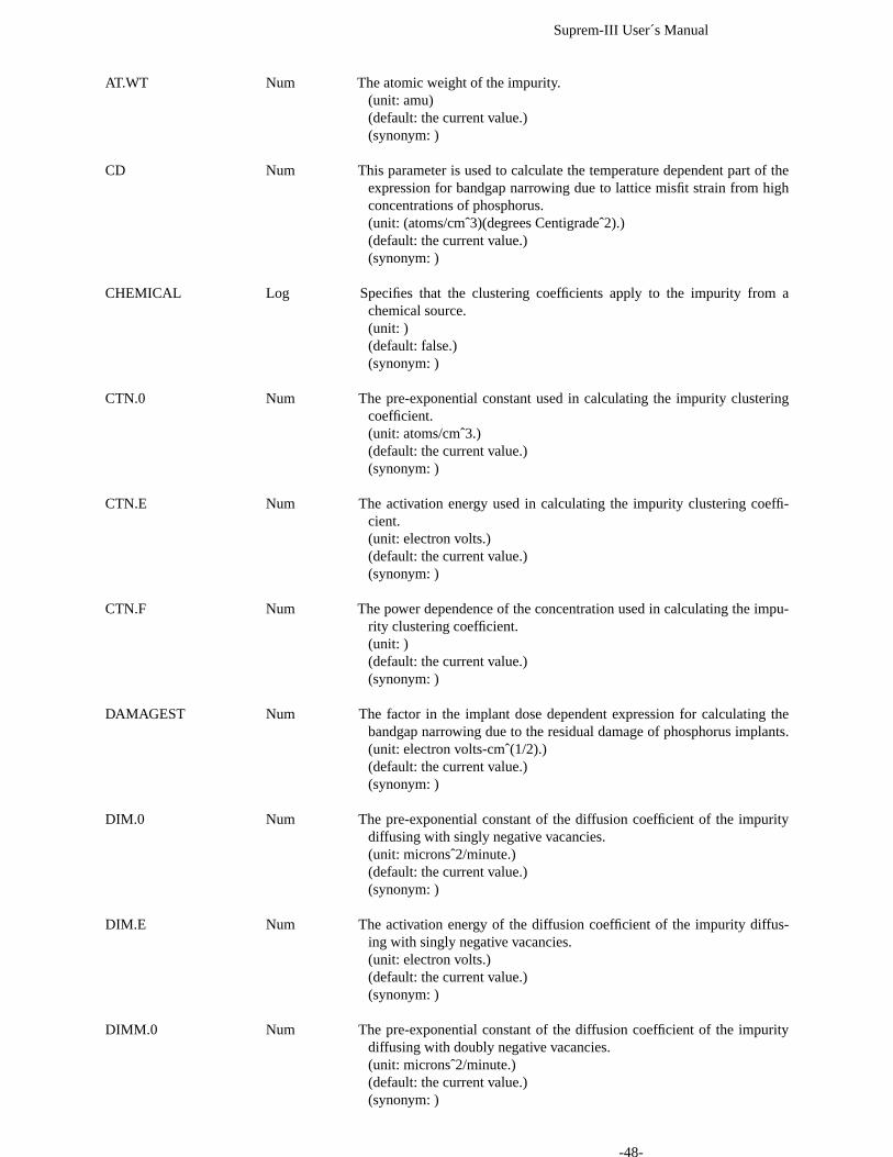
AT .WT Num The atomic weight of the impurity.(unit: amu)(default: the current value.)(synonym: )
CD Num This parameter is used to calculate the temperature dependent part of theexpression for bandgap narrowing due to lattice misfit strain from highconcentrations of phosphorus.(unit: (atoms/cmˆ3)(degrees Centigradeˆ2).)(default: the current value.)(synonym: )
CHEMICAL Log Specifies that the clustering coefficients apply to the impurity from achemical source.(unit: )(default: false.)(synonym: )
CTN.0 Num The pre-exponential constant used in calculating the impurity clusteringcoefficient.(unit: atoms/cmˆ3.)(default: the current value.)(synonym: )
CTN.E Num The activation energy used in calculating the impurity clustering coeffi-cient.(unit: electron volts.)(default: the current value.)(synonym: )
CTN.F Num The power dependence of the concentration used in calculating the impu-rity clustering coefficient.(unit: )(default: the current value.)(synonym: )
DAMAGEST Num The factor in the implant dose dependent expression for calculating thebandgap narrowing due to the residual damage of phosphorus implants.(unit: electron volts-cmˆ(1/2).)(default: the current value.)(synonym: )
DIM.0 Num The pre-exponential constant of the diffusion coefficient of the impuritydiffusing with singly negative vacancies.(unit: micronsˆ2/minute.)(default: the current value.)(synonym: )
DIM.E Num The activation energy of the diffusion coefficient of the impurity diffus-ing with singly negative vacancies.(unit: electron volts.)(default: the current value.)(synonym: )
DIMM.0 Num The pre-exponential constant of the diffusion coefficient of the impuritydiffusing with doubly negative vacancies.(unit: micronsˆ2/minute.)(default: the current value.)(synonym: )
-48-
Suprem-III User´s Manual
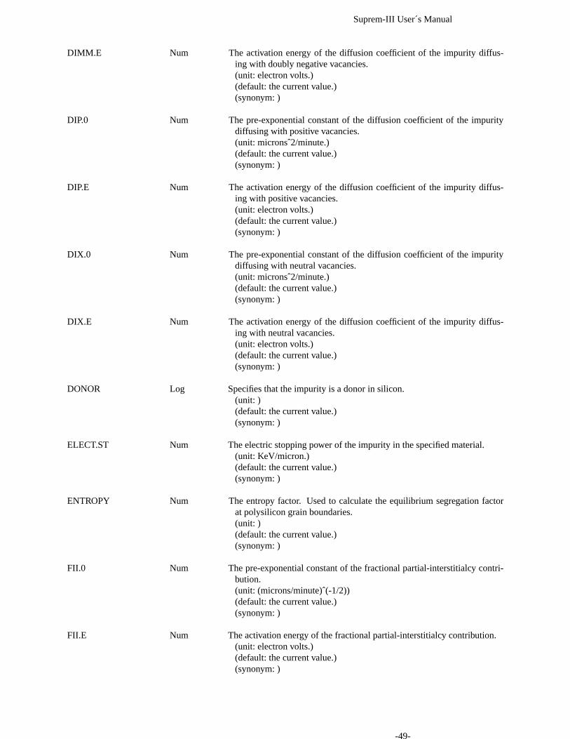
DIMM.E Num The activation energy of the diffusion coefficient of the impurity diffus-ing with doubly negative vacancies.(unit: electron volts.)(default: the current value.)(synonym: )
DIP.0 Num The pre-exponential constant of the diffusion coefficient of the impuritydiffusing with positive vacancies.(unit: micronsˆ2/minute.)(default: the current value.)(synonym: )
DIP.E Num The activation energy of the diffusion coefficient of the impurity diffus-ing with positive vacancies.(unit: electron volts.)(default: the current value.)(synonym: )
DIX.0 Num The pre-exponential constant of the diffusion coefficient of the impuritydiffusing with neutral vacancies.(unit: micronsˆ2/minute.)(default: the current value.)(synonym: )
DIX.E Num The activation energy of the diffusion coefficient of the impurity diffus-ing with neutral vacancies.(unit: electron volts.)(default: the current value.)(synonym: )
DONOR Log Specifies that the impurity is a donor in silicon.(unit: )(default: the current value.)(synonym: )
ELECT.ST Num The electric stopping power of the impurity in the specified material.(unit: KeV/micron.)(default: the current value.)(synonym: )
ENTROPY Num The entropy factor. Used to calculate the equilibrium segregation factorat polysilicon grain boundaries.(unit: )(default: the current value.)(synonym: )
FII.0 Num The pre-exponential constant of the fractional partial-interstitialcy contri-bution.(unit: (microns/minute)ˆ(-1/2))(default: the current value.)(synonym: )
FII.E Num The activation energy of the fractional partial-interstitialcy contribution.(unit: electron volts.)(default: the current value.)(synonym: )
-49-
Suprem-III User´s Manual
HEAT.SEG Num The activation energy of the equilibrium segregation factor at polysilicongrain boundaries.(unit: electron volts.)(default: the current value.)(synonym: )
IMPLANT Log Specifies that the impurity clustering coefficients apply to the impurityfrom an implanted source.(unit: )(default: false.)(synonym: )
IONFILE1 Char Specifies the primary ion implant range data file for implants using theanalytic distributions. This file will be searched for the range statisticswhen implanting the atomic ion of this impurity.(unit: )(default: the last file specified.)(synonym: )
IONFILE2 Char Specifies the secondary ion implant range data file for implants using theanalytic distributions. This file will be searched for the range statisticswhen implanting the compound ions containing this impurity.(unit: )(default: the last file specified.)(synonym: )
K.A Num Used in R. Reif’s epitaxial doping model (see reference in EPITAXYstatement). K.a is a thermodynamic constant relating the dopantspecies concentration in solid silicon and adsorbed layer.(unit: centimeters)(default: the current value.)(synonym: )
K.MF Num Used in R. Reif’s epitaxial doping model (see reference in EPITAXYstatement). K.mf is a kinetic coefficient controling the rate-limitingstep of the dopant incorporation process.(unit: centimetersˆ(-2) minutesˆ(-1) atmospheresˆ(-1))(default: the current value.)(synonym: )
K.P Num Used in R. Reif’s epitaxial doping model (see reference in EPITAXYstatement). K.p is a thermodynamic constant relating the dopantspecies concentration in solid silicon and gas phase.(unit: centimetersˆ(-3) atmospheresˆ(-1))(default: the current value.)(synonym: )
MISFITST Num The prefactor in the high concentration dependent expression for calcu-lating the bandgap narrowing due to the lattice misfit strain from highconcentrations of phosphorus.(unit: electron volts-cmˆ3.)(default: the current value.)(synonym: )
MSF100FA Num The orientation factor in <100> orientation silicon for bandgap narrowingdue to lattice misfit strain from high concentrations of phosphorus.(unit: )(default: the current value.)(synonym: )
-50-

Suprem-III User´s Manual
MSF110FA Num The orientation factor in <110> orientation silicon for bandgap narrowingdue to lattice misfit strain from high concentrations of phosphorus.(unit: )(default: the current value.)(synonym: )
MSF111FA Num The orientation factor in <111> orientation silicon for bandgap narrowingdue to lattice misfit strain from high concentrations of phosphorus.(unit: )(default: the current value.)(synonym: )
NAME Char The name of the impurity.(unit: )(default: the last name specified.)(synonym: )
NE.0 Num The pre-exponential constant for Ne, the concentration at which theP+V= pairs disassociate. Used to calculate the diffusivity of phospho-rus at high concentrations.(unit: atoms/cmˆ3.)(default: the current value.)(synonym: )
NE.E Num The activation energy for calculating Ne, the concentration at which theP+V= pairs disassociate. Used to calculate the diffusivity of phospho-rus at high concentrations.(unit: electron volts.)(default: the current value.)(synonym: )
NITRIDE Log Specifies that the material dependent parameters apply to the impurity insilicon nitride.(unit: )(default: false.)(synonym: )
OXIDE Log Specifies that the material dependent parameters apply to the impurity insilicon dioxide.(unit: )(default: false.)(synonym: )
POLYSILI Log Specifies that the material dependent parameters apply to the impurity inpolysilicon.(unit: )(default: false.)(synonym: )
Q.SITES Num Effective density of segregation sites at a grain boundary.(unit: sites/cmˆ2.)(default: the current value.)(synonym: )
SILICON Log Specifies that the material dependent parameters apply to the impurity insingle crystal silicon.(unit: )(default: false.)(synonym: )
-51-

Suprem-III User´s Manual
The IMPURITY statement is used to input or modify the coefficients and parameters that define a givenimpurity. Four impurities are defined, boron, phosphorus, arsenic, and antimony. These impurities each have theirown impurity coefficient statements which are aliases of the general IMPURITY statement.
-52-
Suprem-III User´s Manual
26. Initialize Statement----------------------------
The INITIALIZE statement, as it’s name implies, is used to set up the initial coefficients and structure tobe used in the processing steps that follow.
INITIALIZE
[ ( COEFFICI=<c> | FIRSTIME ) ][ STRUCTUR=<c> ] [ MIN.DX=<n> ] [ SAVESTEP ][ THICKNES=<n> ] [ DX=<n> ] [ XDX=<n> ] [ SPACES=<n> ][ ( SILICON ( <111> | <110> | <100> )
| POLYSILI( GRAINSIZ=<n> | ( TEMPERAT=<n> [ PRESSURE=<n> ] ) )
| OXIDE| NITRIDE| ALUMINUM)[ CONCENTR=<n>( ANTIMONY | ARSENIC | BORON | PHOSPHOR )
]]
Name Type Description---- ---- -----------
ALUMINUM Log Specifies that aluminum is the material in the first layer.(unit: )(default: false.)(synonym: )
ANTIMONY Log Specified that the initial structure is to be doped uniformly with antimo-ny.(unit: )(default: false.)(synonym: SB)
ARSENIC Log Specifies that the initial structure is to be doped uniformly with arsenic.(unit: )(default: false.)(synonym: AS)
BORON Log Specifies that the initial structure is to be doped uniformly with boron.(unit: )(default: false.)(synonym: )
COEFFICI Char The name of the file containing the physical coefficients to be used by theprogram.(unit: )(default: S3cof0.)(synonym: )
-53-

Suprem-III User´s Manual
CONCENTR Num The impurity concentration at which the structure is to be uniformlydoped.(unit: atoms/cmˆ3.)(default: 0.0)(synonym: )
DX Num The nominal grid spacing to be used in the first layer of the structure atthe location specified by XDX.(unit: microns.)(default: That of the first layer of the input structure file; otherwise, thedefault for the material in the first layer.)(synonym: )
FIRSTIME Log Indicates that no coefficient file exists. Used the first time the program isexecuted to create the default coefficient file.(unit: )(default: false.)(synonym: )
GRAINSIZ Num Specifies the polysilicon grain size.(unit: microns.)(default: )(synonym: )
MIN.DX Num The minimum grid spacing to be used in the first layer of the structure.(unit: microns.)(default: That of the first layer of the input structure file; otherwise,0.001.)(synonym: )
NITRIDE Log Specifies that silicon nitride is the material in the first layer.(unit: )(default: false.)(synonym: )
OXIDE Log Specifies that silicon dioxide is the material in the first layer.(unit: )(default: false.)(synonym: )
PHOSPHOR Log Specifies that the initial structure is to be doped uniformly with phospho-rus.(unit: )(default: false.)(synonym: )
POLYSILI Log Specifies that polycrystalline silicon is the material in the first layer.(unit: )(default: false.)(synonym: )
PRESSURE Num Specifies the polysilicon deposition pressure.(unit: atmospheres.)(default: 1.0)(synonym: )
-54-

Suprem-III User´s Manual
SAVESTEP Log Causes the structure to be saved in the file S3sav0 after each step inwhich the structure is modified.(unit: )(default: false.)(synonym: )
SILICON Log Specifies that single crystal silicon is the material in the first layer.(unit: )(default: false.)(synonym: )
SPACES Num The number of spaces to be used in the layer.(unit: )(default: thickness/dx if no structure is input; otherwise, the currentnumber of spaces.)(synonym: )
STRUCTUR Char The name of the file containing the initial structure information.(unit: )(default: )(synonym: )
TEMPERAT Num Specifies the polysilicon deposition temperature.(unit: degrees Centigrade.)(default: )(synonym: )
THICKNES Num The thickness of the first layer of the initial structure.(unit: microns.)(default: That of the first layer of the input structure file; otherwise,none.)(synonym: )
XDX Num The distance from the top of the first layer at which the nominal gridspacing applies.(unit: microns.)(default: That of the first layer of the input structure file; otherwise, 0.0)(synonym: )
<100> Log Specifies that the crystalline orientation of the material in the first layer is<100>.(unit: )(default: false.)(synonym: )
<110> Log Specifies that the crystalline orientation of the material in the first layer is<110>.(unit: )(default: false.)(synonym: )
<111> Log Specifies that the crystalline orientation of the material in the first layer is<111>.(unit: )(default: false.)(synonym: )
-55-
Suprem-III User´s Manual
An INITIALIZE statement is required in every SUPREM-III input sequence and it must preceed all otherstatements except for TITLE or COMMENT statements. At the start of execution the SUPREM-III program con-tains no information about any of the materials or impurities that may be used in the processing sequence. All of thephysical and model coefficients and any initial structure information is contained in one or two files and must beread into the programs internal storage before processing can proceed. Normally, all of the coefficient information iscontained in a default file, S3COF0. If this is the case, and if a coefficient file is not specified in the INITIALIZEstatement, the data is read from the default coefficient file.
The same is true with the structure information, an initial structure of at least one layer of material must bepresent before execution can continue. A previously defined structure of arbitrary complexity can be input from afile specified by the STRUCTUR parameter. The other parameters of the INITIALIZE statement may be used to re-define the structure input from a file if the structure has only a single layer of material or, if no structure file is input,they may be used to set up the initial layer.
If no coefficient file is present, the FIRSTIME parameter must be specified and all of the needed coeffi-cients explicitly specified by subsequent statements before processing statements can be executed. As it’s name im-plies, the FIRSTIME parameter should only be needed the first time the program is brought up at a new installation.
-56-

Suprem-III User´s Manual
27. Loadfile Statement----------------------------
The LOADFILE statement is used to input either a new structure to be processed, the physical and modelcoefficients to be used by the program, or both.
LOADFILE
FILENAME=<c> ( ALL | COEFFICI | STRUCTUR )[ FORMATTE ]
Name Type Description---- ---- -----------
ALL Log Specifies that both the structure information and the model coefficientsare to be input from the specified file.(unit: )(default: false.)(synonym: )
COEFFICI Log Specifies that the coefficient information is to be input from the specifiedfile.(unit: )(default: false.)(synonym: )
FILENAME Char The name of the file from which the specified information is to be read.(unit: )(default: )(synonym: NAME)
FORMATTE Log Specifies that the information in the file is formatted. If not specifiedthen the information is assumed to be unformatted or binary.(unit: )(default: false.)(synonym: )
STRUCTUR Log Specifies that the information describing the structure is to be input fromthe specified file.(unit: )(default: false.)(synonym: )
The LOADFILE statement inputs two classes of information about the process that is to be simulated. Thefirst class is the physical structure and impurity distributions of the materials to be simulated. This file is used as thestarting point for subsequent processing steps. The other class of information consists of all of the physical andmodel parameters or coefficients used by the program.
A LOADFILE statement may appear at any point in a processing sequence after the INITIALIZE state-ment and before the STOP statement. If both structure and coefficient information are to be input, it is recommend-ed that an INITIALIZE statement be used instead of LOADFILE.
-57-

Suprem-III User´s Manual
28. Lpplot Statement--------------------------
The LPPLOT statement outputs a semi-logarithmic plot of the specified impurity concentrations versusdepth into the structure to the output using the standard character set. This type of plotting is suitable for non-graph-ics terminals and line printers.
PLOT
[ ACTIVE ] [ CHEMICAL ] [ TOTAL ] [ NET ][ ANTIMONY ] [ ARSENIC ] [ BORON ] [ PHOSPHOR ][ XMIN=<n> ] [ XMAX=<n> ] [ CMIN=<n> ] [ CMAX=<n> ][ LINES/PA=<n> ] [ COLUMNS=<n> ]
Name Type Description---- ---- -----------
ACTIVE Log Specifies that the electrically active concentrations of the specified impu-rities are to be plotted.(unit: )(default: false.)(synonym: )
ANTIMONY Log Specifies that the antimony concentration, either active and/or chemical,is to be plotted.(unit: )(default: false.)(synonym: SB)
ARSENIC Log Specifies that the arsenic concentration, either active and/or chemical, isto be plotted.(unit: )(default: false.)(synonym: AS)
BORON Log Specifies that the boron concentration, either active and/or chemical, is tobe plotted.(unit: )(default: false.)(synonym: )
CHEMICAL Log Specifies that the chemical concentration of the specified impurities areto be plotted.(unit: )(default: false.)(synonym: )
COLUMNS Num The number of character columns of the output device.(unit: columns)(default: 80)(synonym: )
CMAX Num The maximum concentration value plotted.(unit: atoms/cmˆ3.)(default: 1x10ˆ21)(synonym: )
-58-

Suprem-III User´s Manual
CMIN Num The minimum concentration value plotted.(unit: atoms/cmˆ3.)(default: 1x10ˆ14)(synonym: )
LINES/PA Num The number of line per page of the output device.(unit: lines)(default: 60)(synonym: )
NET Log Specifies that the difference of the sum of the n-type and the sum p-typeactive or chemical impurity concentrations present in the structure is tobe plotted.(unit: )(default: false.)(synonym: )
PHOSPHOR Log Specifies that the phosphorus concentration, either active and/or chemi-cal, is to be plotted.(unit: )(default: false.)(synonym: )
TOTAL Log Specifies that the sum of the active or chemical impurity concentrationspresent in the structure is to be plotted.(unit: )(default: false.)(synonym: )
XMAX Num The distance from the top of the plotted layers to the point where the lastconcentration is to be plotted.(unit: microns.)(default: The current total width of the plotted layers.)(synonym: )
XMIN Num The distance from the top of the plotted layers to the point where the firstconcentration is to be plotted.(unit: microns.)(default: 0.0)(synonym: )
The LPPLOT statement is used to output plots of the impurity distributions versus distance in the struc-ture. The impurities present may be plotted either individually, added together, or as the difference between n- andp-type dopants. These plots may be of either the electrically active or total chemical concentrations.
If no range parameters (XMIN or XMAX) are specified, then the distributions are plotted over the entirestructure. If no minimum or maximum plot concentrations (CMIN or CMAX) are specified, then the range between1x10ˆ14 and 1x10ˆ21 is plotted.
-59-

Suprem-III User´s Manual
29. Material Statement----------------------------
The MATERIAL statement is used to input or modify the characteristics of a layer material. The programis presently configured to handle up to ten different material types. Materials with index numbers one through fiveare defaulted to silicon, silicon dioxide, polysilicon, silicon nitride, and aluminum, respectively. The parameter val-ues for the defaulted materials may also be accessed via the SILICON, OXIDE, POLYSILI, NITRIDE, and ALU-MINUM statements.
MATERIAL
[ INDEX=<n> ][ NAME=<c> ] [ DX.DEFAU=<n> ][ ( SEMICOND | CONDUCTO | INSULATO ) ][ SPECIES=<n> ] [ DENSITY=<n> ][ AT.WT.1=<n> ] [ AT.WT.2=<n> ] [ AT.WT.3=<n> ][ AT.NUM.1=<n> ] [ AT.NUM.2=<n> ] [ AT.NUM.3=<n> ][ ABUND.1=<n> ] [ ABUND.2=<n> ] [ ABUND.3=<n> ][ DIFX.0=<n> ] [ DIFX.E=<n> ][ DIMX.0=<n> ] [ DIFM.E=<n> ][ DIMMX.0=<n> ] [ DIFMM.E=<n> ][ DIFP.0=<n> ] [ DIFP.E=<n> ][ NI.0=<n> ] [ NI.E=<n> ] [ NI.F=<n> ] [ DEFECTLN=<n> ][ OEDK.0=<n> ] [ OEDK.E=<n> ] [ OED.RATE=<n> ][ 100.OEDF=<n> ] [ 110.OEDF=<n> ] [ 111.OEDF=<n> ][ GSZ.H.0=<n> ] [ GSZ.H.E=<n> ][ GSZ.L.0=<n> ] [ GSZ.L.E=<n> ][ MIN.GRAI=<n> ] [ TEMP.BRE=<n> ][ RATIO.0=<n> ] [ RATIO.E=<n> ][ GEO.FACT=<n> ] [ GBE.0=<n> ] [ GBE.E=<n> ][ TAU.0=<n> ] [ TAU.E=<n> ][ AFFINITY=<n> ] [ WORK.FUN=<n> ] [ EPSILONF=<n> ][ N.VALENC=<n> ] [ N.CONDUC=<n> ] [ BAND.GAP=<n> ][ K.M=<n> ]
Name Type Description---- ---- -----------
ABUND.1 Num The relative abundance of element one in the material. The sum of allabundances for a material must equal one.(unit: )(default: the current value.)(synonym: )
ABUND.2 Num The relative abundance of element two in the material. The sum of allabundances for a material must equal one.(unit: )(default: the current value.)(synonym: )
ABUND.3 Num The relative abundance of element three in the material. The sum of allabundances for a material must equal one.(unit: )(default: the current value.)(synonym: )
-60-

Suprem-III User´s Manual
AFFINITY Num The electron affinity of the material.(unit: electron volts.)(default: the current value.)(synonym: )
AT .NUM.1 Num The atomic number of element one in the material.(unit: )(default: the current value.)(synonym: )
AT .NUM.2 Num The atomic number of element two in the material.(unit: )(default: the current value.)(synonym: )
AT .NUM.3 Num The atomic number of element three in the material.(unit: )(default: the current value.)(synonym: )
AT .WT.1 Num The atomic weight of element one in the material.(unit: amu)(default: the current value.)(synonym: )
AT .WT.2 Num The atomic weight of element two in the material.(unit: amu)(default: the current value.)(synonym: )
AT .WT.3 Num The atomic weight of element three in the material.(unit: amu)(default: the current value.)(synonym: )
BAND.GAP Num The band gap of the material.(unit: electron volts.)(default: the current value.)(synonym: )
CONDUCTO Num Specifies that the material is a conductor.(unit: )(default: false.)(synonym: )
DEFECTLN Num The decay length of point defects in the material.(unit: microns)(default: the current value.)(synonym: )
DENSITY Num The density of the material.(unit: grams/cmˆ3.)(default: the current value.)(synonym: )
-61-

Suprem-III User´s Manual
DIFM.0 Num The pre-exponential constant used in the calculation the component ofthe self-diffusivity due to diffusion with singly negative vacancies.(unit: micronsˆ2/minute.)(default: the current value.)(synonym: )
DIFM.E Num The activation energy used in the calculation the component of the self-diffusivity due to diffusion with singly negative vacancies.(unit: electron volts.)(default: the current value.)(synonym: )
DIFMM.0 Num The pre-exponential constant used in the calculation of the component ofthe self-diffusivity due to diffusion with doubly negative vacancies.(unit: micronsˆ2/minute.)(default: the current value.)(synonym: )
DIFMM.E Num The activation energy used in the calculation the component of the self-diffusivity due to diffusion with doubly negative vacancies.(unit: electron volts.)(default: the current value.)(synonym: )
DIFP.0 Num The pre-exponential constant used in the calculation the component ofthe self-diffusivity due to diffusion with positive vacancies.(unit: micronsˆ2/minute.)(default: the current value.)(synonym: )
DIFP.E Num The activation energy used in the calculation the component of the self-diffusivity due to diffusion with positive vacancies.(unit: electron volts.)(default: the current value.)(synonym: )
DIFX.0 Num The pre-exponential constant used in the calculation of the component ofthe self-diffusivity due to diffusion with neutral vacancies.(unit: micronsˆ2/minute.)(default: the current value.)(synonym: )
DIFX.E Num The activation energy used in the calculation of the component of theself-diffusivity due to diffusion with neutral vacancies.(unit: electron volts.)(default: the current value.)(synonym: )
DX.DEFAU Num The default nominal grid spacing for any layer containing this material.(unit: microns.)(default: the current value.)(synonym: )
EPSILONF Num The dielectric constant of the material relative the dielectric constant ofair.(unit: )(default: the current value.)(synonym: )
-62-

Suprem-III User´s Manual
GBE.0 Num The pre-exponential constant used in calculating the grain-boundary en-ergy(unit: )(default: the current value.)(synonym: )
GBE.E Num The activation energy used in calculating the grain-boundary energy.(unit: electron volts.)(default: the current value.)(synonym: )
GEO.FACT Num A geometric factor used in calculating the grain growth driving force, F.(unit: )(default: the current value.)(synonym: )
GSZ.H.0 Num The pre-exponential constant used in calculating the ‘as deposited’polysilicon grain size for pressures near one atmosphere.(unit: microns.)(default: the current value.)(synonym: )
GSZ.H.E Num The activation energy used in calculating the ‘as deposited’ polysilicongrain size for pressures near one atmosphere.(unit: electron volts.)(default: the current value.)(synonym: )
GSZ.L.0 Num The pre-exponential constant used in calculating the ‘as deposited’polysilicon grain size for low pressure CVD.(unit: microns.)(default: the current value.)(synonym: )
GSZ.L.E Num The activation energy used in calculating the ‘as deposited’ polysilicongrain size for low pressure CVD.(unit: electron volts.)(default: the current value.)(synonym: )
INDEX Num The material index of the material being modified. This number is usedinternally in the program to identify the material and point to its param-eters.(unit: )(default: )(synonym: )
INSULATO Log Specifies that the material is an insulator.(unit: )(default: false.)(synonym: )
K.M Num Used in R. Reif’s epitaxial growth model (see reference in EPITAXYstatement). K.m is the mass transport coefficient for silane in hydro-gen.(unit: microns/minute/atmosphere)(default: the current value)(synonym: )
-63-

Suprem-III User´s Manual
MIN.GRAI Num The minimum polysilicon grain size. Used for ‘as deposited’ LPCVDpolysilicon when the temperature is below that specified by TEMP.BRE(unit: microns)(default: the current value.)(synonym: )
NAME Char The name of the material.(unit: )(default: the current name of the material.)(synonym: )
NI.0 Num The pre-factor used in the calculation of the intrinsic carrier concentra-tion.(unit: (carriers/cmˆ3)(degrees Kelvin)ˆ(3/2).)(default: the current value.)(synonym: )
NI.E Num The activation energy used in the calculation of the intrinsic carrier con-centration.(unit: electron volts.)(default: the current value.)(synonym: )
NI.F Num The exponent to the absolute temperature used in the calculation of theintrinsic carrier concentration.(unit: )(default: the current value.)(synonym: )
N.VALENC Num The carrier concentration in the valence band of the material.(unit: carriers/cmˆ3.)(default: the current value.)(synonym: )
N.CONDUC Num The carrier concentration in the conduction band of the material.(unit: carriers/cmˆ3.)(default: the current value.)(synonym: )
OEDK.0 Num The pre-exponential constant used to calculate the relative contribution ofoxidation enhanced diffusion to intrinsic diffusion.(unit: )(default: the current value.)(synonym: )
OEDK.E Num The activation energy used to calculate the relative contribution of oxida-tion enhanced diffusion to intrinsic diffusion.(unit: electron volts)(default: the current value.)(synonym: )
OED.RATE Num The power dependence of oxidation enhanced diffusion on the oxidationrate.(unit: )(default: the current value.)(synonym: )
-64-

Suprem-III User´s Manual
RATIO.0 Num The pre-exponential constant used to calculate the ratio of the siliconself-diffusivities in the grain and in the bulk. Actually the ratio of thepre-exponential factors for the two self-diffusivities(unit: )(default: the current value.)(synonym: )
RATIO.E Num The activation energy used to calculate the ratio of the silicon self-diffu-sivities in the grain and in the bulk. Actually the difference betweenthe activation energies of the two self-diffusivities(unit: electron volts.)(default: the current value.)(synonym: )
SEMICOND Log Specifies that the material is a semiconductor.(unit: )(default: false.)(synonym: )
SPECIES Num The number of different elements in this material.(unit: )(default: the current value.)(synonym: )
TA U.0 Num The pre-exponential constant used to calculate the time dependence ofthe grain interior concentration.(unit: minutes.)(default: the current value.)(synonym: )
TA U.E Num The activation energy used to calculate the time dependence of the graininterior concentration.(unit: electron volts.)(default: the current value.)(synonym: )
TEMP.BRE Num For LPCVD the temperature below which the deposited polysilicon be-comes amorphous.(unit: degrees Centigrade.)(default: the current value.)(synonym: )
WORK.FUN Num The work function of the material.(unit: volts)(default: the current value.)(synonym: )
100.OEDF Num The orientation dependent factor for the oxidation enhanced diffusion for<100> oriented silicon.(unit: )(default: the current value.)(synonym: )
110.OEDF Num The orientation dependent factor for the oxidation enhanced diffusion for<110> oriented silicon.(unit: )(default: the current value.)(synonym: )
-65-

Suprem-III User´s Manual
111.OEDF Num The orientation dependent factor for the oxidation enhanced diffusion for<111> oriented silicon.(unit: )(default: the current value.)(synonym: )
The MATERIAL statement is used to input or modify the coefficients and parameters that define a givenmaterial. Up to ten materials can be defined at one time. There are five default materials assigned the material in-dexes one through ten, these are single crystal silicon, silicon dioxide, polysilicon, silicon nitride, and aluminum.The first four of these should not be redefined as they are treated specially by several models in the program.
The current implementation of the program allows the definition of materials made up of at most three ele-ments.
-66-
Suprem-III User´s Manual
30. Nitride Statement--------------------------
The NITRIDE statement is used to input or modify the characteristics of silicon nitride as a layer material.
NITRIDE
[ NAME=<c> ] [ DX.DEFAU=<n> ][ INSULATO ][ SPECIES=<n> ] [ DENSITY=<n> ][ AT.WT.1=<n> ] [ AT.WT.2=<n> ][ AT.NUM.1=<n> ] [ AT.NUM.2=<n> ][ ABUND.1=<n> ] [ ABUND.2=<n> ][ EPSILONF=<n> ]
Name Type Description---- ---- -----------
ABUND.1 Num The relative abundance of element one in the material. The sum of allabundances for a material must equal one.(unit: )(default: the current value.)(synonym: )
ABUND.2 Num The relative abundance of element two in the material. The sum of allabundances for a material must equal one.(unit: )(default: the current value.)(synonym: )
AT .NUM.1 Num The atomic number of element one in the material.(unit: )(default: the current value.)(synonym: )
AT .NUM.2 Num The atomic number of element two in the material.(unit: )(default: the current value.)(synonym: )
AT .WT.1 Num The atomic weight of element one in the material.(unit: amu)(default: the current value.)(synonym: )
AT .WT.2 Num The atomic weight of element two in the material.(unit: amu)(default: the current value.)(synonym: )
DENSITY Num The density of the material.(unit: grams/cmˆ3.)(default: the current value.)(synonym: )
-67-
Suprem-III User´s Manual
DX.DEFAU Num The default nominal grid spacing for any layer containing this material.(unit: microns.)(default: the current value.)(synonym: )
EPSILONF Num The dielectric constant of the material relative the dielectric constant ofair.(unit: )(default: the current value.)(synonym: )
INSULATO Log Specifies that the material is an insulator.(unit: )(default: false.)(synonym: )
NAME Char The name of the material.(unit: )(default: the current name of the material.)(synonym: )
SPECIES Num The number of different elements in this material.(unit: )(default: the current value.)(synonym: )
The NITRIDE statement is an alias for the MATERIAL statement with an index of four and is used to de-fine or modify the parameters and coefficients associated with the material silicon nitride. Not all of the parametersof the MATERIAL statement apply to silicon nitride and so are not listed here.
-68-

Suprem-III User´s Manual
31. Nitrogen Statement----------------------------
The NITROGEN statement allows the user to modify the coefficients used to model the oxidation of thevarious materials under nitrogen ambient or non-oxidizing conditions.
NITROGEN
[ ( <111> | <110> | <100> )[ LIN.L.0=<n> ] [ LIN.L.E=<n> ][ LIN.H.0=<n> ] [ LIN.H.E=<n> ][ THINOX.0=<n> ] [ THINOX.E=<n> ] [ THINOX.L=<n> ]
][ PAR.L.0=<n> ] [ PAR.L.E=<n> ][ PAR.H.0=<n> ] [ PAR.H.E=<n> ][ LIN.BREA=<n> ] [ PAR.BREA=<n> ][ LIN.PDEP=<n> ] [ PAR.PDEP=<n> ][ PRESSURE=<n> ] [ HCL%=<n> ][ GAMMA.0=<n> ] [ GAMMA.E=<n> ][ DELTA.0=<n> ] [ DELTA.E=<n> ][ EXP.0=<n> ] [ EXP.E=<n> ][ NIOX.0=<n> ] [ NIOX.E=<n> ] [ NIOX.F=<n> ][ CL.ROW=<n> [ CL.PCT=<n> ]CL.COLUM=<n> [ CL.TEMPE=<n> ][ CL.DEP.L=<n> ] [ CL.DEP.P=<n> ]
]
Name Type Description---- ---- -----------
CL.COLUM Num The column number in the table of coefficients used to calculate the chlo-rine dependence of the oxidation rates.(unit: )(default: the current value.)(synonym: )
CL.DEP.L Num The coefficient modifying the linear oxidation rate in the presence ofchlorine at the specified row and column.(unit: )(default: the current value.)(synonym: )
CL.DEP.P Num The coefficient modifying the parabolic oxidation rate in the presence ofchlorine at the specified row and column.(unit: )(default: the current value.)(synonym: )
CL.PCT Num The percentage of chlorine for which the coefficients in the specified roware valid.(unit: percent.)(default: the current value.)(synonym: )
-69-

Suprem-III User´s Manual
CL.ROW Num The row number in the table of coefficients used to calculate the chlorinedependence of the oxidation rates.(unit: )(default: the current value.)(synonym: )
CL.TEMPE Num The temperature for which the coefficients in the specified column arevalid.(unit: degrees Centigrade.)(default: the current value.)(synonym: )
DELTA.0 Num The pre-exponential factor of the delta coefficient used in calculating theimpurity concentration dependence of the parabolic oxidation rate.(unit: cmˆ3/atom.)(default: the current value.)(synonym: )
DELTA.E Num The activation energy of the delta coefficient used in calculating the im-purity concentration dependence of the parabolic oxidation rate.(unit: electron volts.)(default: the current value.)(synonym: )
EXP.0 Num The pre-exponential factor of the exponent used in calculating the impu-rity concentration dependence of the parabolic oxidation rate.(unit: )(default: the current value.)(synonym: )
EXP.E Num The activation energy of the exponent used in calculating the impurityconcentration dependence of the parabolic oxidation rate.(unit: electron volts.)(default: the current value.)(synonym: )
GAMMA.0 Num The pre-exponential factor of the gamma coefficient used in calculatingthe impurity concentration dependence of the linear oxidation rate.(unit: )(default: the current value.)(synonym: )
GAMMA.E Num The activation energy of the gamma coefficient used in calculating theimpurity concentration dependence of the linear oxidation rate.(unit: electron volts.)(default: the current value.)(synonym: )
HCL% Num The default percentage of chlorine present in the ambient.(unit: percent.)(default: the current value.)(synonym: )
LIN.BREA Num The temperature at which the temperature dependence of the linear oxi-dation rate changes.(unit: degrees Centigrade.)(default: the current value.)(synonym: )
-70-

Suprem-III User´s Manual
LIN.H.0 Num The pre-exponential constant of the linear oxidation rate for temperaturesabove the breakpoint set by L.BREAKP.(unit: microns/minute.)(default: the current value.)(synonym: )
LIN.H.E Num The activation energy of the linear oxidation rate for temperatures abovethe breakpoint set by L.BREAKP.(unit: electron volts.)(default: the current value.)(synonym: )
LIN.L.0 Num The pre-exponential constant of the linear oxidation rate for temperaturesbelow the breakpoint set by L.BREAKP.(unit: microns/minute.)(default: the current value.)(synonym: )
LIN.L.E Num The activation energy of the linear oxidation rate for temperatures belowthe breakpoint set by L.BREAKP.(unit: electron volts.)(default: the current value.)(synonym: )
LIN.PDEP Num The pressure dependence factor for the linear oxidation rate.(unit: )(default: the current value.)(synonym: )
NIOX.0 Num The pre-exponential constant used to determine the oxidation rate of sili-con nitride.(unit: microns.)(default: the current value.)(synonym: )
NIOX.E Num The activation energy used to determine the oxidation rate of silicon ni-tride.(unit: electron volts.)(default: the current value.)(synonym: )
NIOX.F Num The exponent factor used to determine the oxidation rate of silicon ni-tride.(unit: )(default: the current value.)(synonym: )
PAR.BREA Num The temperature at which the temperature dependence of the parabolicoxidation rate changes.(unit: degrees Centigrade.)(default: the current value.)(synonym: )
PAR.H.0 Num The pre-exponential constant of the parabolic oxidation rate for tempera-tures above the breakpoint set by P.BREAKP.(unit: micronsˆ2/minute.)(default: the current value.)(synonym: )
-71-

Suprem-III User´s Manual
PAR.H.E Num The activation energy of the parabolic oxidation rate for temperaturesabove the breakpoint set by P.BREAKP.(unit: electron volts.)(default: the current value.)(synonym: )
PAR.L.0 Num The pre-exponential constant of the parabolic oxidation rate for tempera-tures below the breakpoint set by P.BREAKP.(unit: micronsˆ2/minute.)(default: the current value.)(synonym: )
PAR.L.E Num The activation energy of the parabolic oxidation rate for temperatures be-low the breakpoint set by P.BREAKP.(unit: electron volts.)(default: the current value.)(synonym: )
PAR.PDEP Num The pressure dependence factor for the parabolic oxidation rate.(unit: )(default: the current value.)(synonym: )
PRESSURE Num The default ambient pressure.(unit: atmospheres.)(default: the current value.)(synonym: )
THINOX.0 Num The pre-exponential constant of the thin oxide growth rate parameter.(unit: microns/minute.)(default: the current value.)(synonym: )
THINOX.E Num The activation energy of the thin oxide growth rate parameter.(unit: electron volts.)(default: the current value.)(synonym: )
THINOX.L Num The characteristic length of the thin oxide growth rate parameter.(unit: microns.)(default: the current value.)(synonym: )
<100> Log Specifies that the linear growth rate and thin oxide growth rate parame-ters apply to <100> orientation silicon.(unit: )(default: false.)(synonym: )
<110> Log Specifies that the linear growth rate and thin oxide growth rate parame-ters apply to <110> orientation silicon.(unit: )(default: false.)(synonym: )
<111> Log Specifies that the linear growth rate and thin oxide growth rate parame-ters apply to <111> orientation silicon.(unit: )(default: false.)
-72-

Suprem-III User´s Manual
(synonym: )
The three oxidation model statements, DRYO2, WETO2, and NITROGEN, use identical parameters, dif-fering only in the values assigned. The parameters NIOX.C, NIOX.E, and NIOX.F are used in modeling the oxida-tion of silicon nitride while the others deal with the oxidation of single and polycrystalline silicon.
The effects of chlorine in the ambient gas on the oxidation rate of silicon are currently modeled by an em-pirical expression whose only variable is defined by the L.CLDEP and P.CLDEP for the linear and parabolic ratesrespectively. To date no convenient function is available to calculate the chlorine dependence as a function of tem-perature and amount of chlorine present, therefor a table of values defines the chlorine dependence factors at thosetemperatures and percentages for which reliable data is available. For those temperatures and chlorine percentagesbetween the values in the table, linear interpolation is employed to calculate the value used. For temperatures or per-centages outside the range of values present in the table, the values whose conditions most nearly match the currentconditions are used. For example, if the current conditions are a temperature of 1175 degrees with three percentchlorine, but the highest temperature entry in the table is 1150 degrees and the nearest chlorine percentages are fortwo and four percent, then a value halfway between the values at 1150 degrees and two and four percent chlorinewill be used.
-73-
Suprem-III User´s Manual
32. Oxide Statement-------------------------
The OXIDE statement is used to input or modify the characteristics of silicon dioxide as a layer material.
OXIDE
[ NAME=<c> ] [ DX.DEFAU=<n> ][ INSULATO ][ SPECIES=<n> ] [ DENSITY=<n> ][ AT.WT.1=<n> ] [ AT.WT.2=<n> ][ AT.NUM.1=<n> ] [ AT.NUM.2=<n> ][ ABUND.1=<n> ] [ ABUND.2=<n> ][ EPSILONF=<n> ]
Name Type Description---- ---- -----------
ABUND.1 Num The relative abundance of element one in the material. The sum of allabundances for a material must equal one.(unit: )(default: the current value.)(synonym: )
ABUND.2 Num The relative abundance of element two in the material. The sum of allabundances for a material must equal one.(unit: )(default: the current value.)(synonym: )
AT .NUM.1 Num The atomic number of element one in the material.(unit: )(default: the current value.)(synonym: )
AT .NUM.2 Num The atomic number of element two in the material.(unit: )(default: the current value.)(synonym: )
AT .WT.1 Num The atomic weight of element one in the material.(unit: amu)(default: the current value.)(synonym: )
AT .WT.2 Num The atomic weight of element two in the material.(unit: amu)(default: the current value.)(synonym: )
DENSITY Num The density of the material.(unit: grams/cmˆ3.)(default: the current value.)(synonym: )
-74-

Suprem-III User´s Manual
DX.DEFAU Num The default nominal grid spacing for any layer containing this material.(unit: microns.)(default: the current value.)(synonym: )
EPSILONF Num The dielectric constant of the material relative the dielectric constant ofair.(unit: )(default: the current value.)(synonym: )
INSULATO Log Specifies that the material is an insulator.(unit: )(default: false.)(synonym: )
NAME Char The name of the material.(unit: )(default: the current name of the material.)(synonym: )
SPECIES Num The number of different elements in this material.(unit: )(default: the current value.)(synonym: )
The OXIDE statement is an alias for the MATERIAL statement with an index of two and is used to defineor modify the parameters and coefficients associated with the material silicon dioxide. Not all of the parameters ofthe MATERIAL statement apply to silicon dioxide and so are not listed here.
-75-

Suprem-III User´s Manual
33. Phosphorus Statement--------------------------------
The PHOSPHOR statement is used to input or modify the physical or model coefficients associated withphosphorus as a dopant impurity.
PHOSPHOR
[ NAME=<c> ] [ DONOR ][ AT.WT=<n> ] [ AT.NUMB=<n> ][ IONFILE1=<c> ] [ IONFILE2=<c> ][ ( ( SILICON
[ FII.0=<n> ] [ FII.E=<n> ][ K.MF=<n> ] [ K.A=<n> ] [ K.P=<n> ]
[ MISFITST=<n> ] [ CD=<n> ][ MSF111FA=<n> ] [ MSF110FA=<n> ] [ MSF100FA=<n> ][ DAMAGEST=<n> ][ NE.0=<n> ] [ NE.E=<n> ][ ( IMPLANT | CHEMICAL )[ CTN.0=<n> ] [ CTN.E=<n> ] [ CTN.F=<n> ]
])
| ( POLYSILI[ ENTROPY=<n> ] [ HEAT.SEG=<n> ] [ Q.SITES=<n> ][ FII.0=<n> ] [ FII.E=<n> ][ ( IMPLANT | CHEMICAL )
[ CTN.0=<n> ] [ CTN.E=<n> ] [ CTN.F=<n> ]]
)| ( OXIDE | NITRIDE | ALUMINUM )[ ELECT.ST=<n> ][ DIX.0=<n> ] [ DIX.E=<n> ][ DIM.0=<n> ] [ DIM.E=<n> ][ DIMM.0=<n> ] [ DIMM.E=<n> ]
]
Name Type Description---- ---- -----------
ALUMINUM Log Specifies that the material dependent parameters apply to phosphorus inaluminum.(unit: )(default: false.)(synonym: )
AT .NUMB Num The atomic number of the impurity.(unit: )(default: the current value.)(synonym: )
AT .WT Num The atomic weight of the impurity.(unit: amu)(default: the current value.)(synonym: )
-76-
Suprem-III User´s Manual
CD Num This parameter is used to calculate the temperature dependent part of theexpression for bandgap narrowing due to lattice misfit strain from highconcentrations of phosphorus.(unit: (atoms/cmˆ3)(degrees Centigradeˆ2).)(default: the current value.)(synonym: )
CHEMICAL Log Specifies that the clustering coefficients apply to the impurity from achemical source.(unit: )(default: false.)(synonym: )
CTN.0 Num The pre-exponential constant used in calculating the impurity clusteringcoefficient.(unit: atoms/cmˆ3.)(default: the current value.)(synonym: )
CTN.E Num The activation energy used in calculating the impurity clustering coeffi-cient.(unit: electron volts.)(default: the current value.)(synonym: )
CTN.F Num The power dependence of the concentration used in calculating the impu-rity clustering coefficient.(unit: )(default: the current value.)(synonym: )
DAMAGEST Num The factor in the implant dose dependent expression for calculating thebandgap narrowing due to the residual damage of phosphorus implants.(unit: electron volts-cmˆ(1/2).)(default: the current value.)(synonym: )
DIM.0 Num The pre-exponential constant of the diffusion coefficient of the impuritydiffusing with singly negative vacancies.(unit: micronsˆ2/minute.)(default: the current value.)(synonym: )
DIM.E Num The activation energy of the diffusion coefficient of the impurity diffus-ing with singly negative vacancies.(unit: electron volts.)(default: the current value.)(synonym: )
DIMM.0 Num The pre-exponential constant of the diffusion coefficient of the impuritydiffusing with doubly negative vacancies.(unit: micronsˆ2/minute.)(default: the current value.)(synonym: )
DIMM.E Num The activation energy of the diffusion coefficient of the impurity diffus-ing with doubly negative vacancies.(unit: electron volts.)(default: the current value.)
-77-

Suprem-III User´s Manual
(synonym: )
DIX.0 Num The pre-exponential constant of the diffusion coefficient of the impuritydiffusing with neutral vacancies.(unit: micronsˆ2/minute.)(default: the current value.)(synonym: )
DIX.E Num The activation energy of the diffusion coefficient of the impurity diffus-ing with neutral vacancies.(unit: electron volts.)(default: the current value.)(synonym: )
DONOR Log Specifies that the impurity is a donor in silicon.(unit: )(default: the current value.)(synonym: )
ELECT.ST Num The electric stopping power of the impurity in the specified material.(unit: KeV/micron.)(default: the current value.)(synonym: )
ENTROPY Num The entropy factor. Used to calculate the equilibrium segregation factorat polysilicon grain boundaries.(unit: )(default: the current value.)(synonym: )
FII.0 Num The pre-exponential constant of the fractional partial-interstitialcy contri-bution.(unit: (microns/minute)ˆ(-1/2))(default: the current value.)(synonym: )
FII.E Num The activation energy of the fractional partial-interstitialcy contribution.(unit: electron volts.)(default: the current value.)(synonym: )
HEAT.SEG Num The activation energy of the equilibrium segregation factor at polysilicongrain boundaries.(unit: electron volts.)(default: the current value.)(synonym: )
IMPLANT Log Specifies that the impurity clustering coefficients apply to the impurityfrom an implanted source.(unit: )(default: false.)(synonym: )
IONFILE1 Char Specifies the primary ion implant range data file for implants using theanalytic distributions. This file will be searched for the range statisticswhen implanting atomic phosphorus.(unit: )(default: the last file specified.)(synonym: )
-78-

Suprem-III User´s Manual
IONFILE2 Char Specifies the secondary ion implant range data file for implants using theanalytic distributions. This file will be searched for the range statisticswhen implanting the compound ions containing phosphorus.(unit: )(default: the last file specified.)(synonym: )
K.A Num Used in R. Reif’s epitaxial doping model (see reference in EPITAXYstatement). K.a is a thermodynamic constant relating the dopantspecies concentration in solid silicon and adsorbed layer.(unit: centimeters)(default: the current value.)(synonym: )
K.MF Num Used in R. Reif’s epitaxial doping model (see reference in EPITAXYstatement). K.mf is a kinetic coefficient controlling the rate-limitingstep of the dopant incorporation process.(unit: centimetersˆ(-2) minutesˆ(-1) atmospheresˆ(-1))(default: the current value.)(synonym: )
K.P Num Used in R. Reif’s epitaxial doping model (see reference in EPITAXYstatement). K.p is a thermodynamic constant relating the dopantspecies concentration in solid silicon and gas phase.(unit: centimetersˆ(-3) atmospheresˆ(-1))(default: the current value.)(synonym: )
MISFITST Num The prefactor in the high concentration dependent expression for calcu-lating the bandgap narrowing due to the lattice misfit strain from highconcentrations of phosphorus.(unit: electron volts-cmˆ3.)(default: the current value.)(synonym: )
MSF100FA Num The orientation factor in <100> orientation silicon for bandgap narrowingdue to lattice misfit strain from high concentrations of phosphorus.(unit: )(default: the current value.)(synonym: )
MSF110FA Num The orientation factor in <110> orientation silicon for bandgap narrowingdue to lattice misfit strain from high concentrations of phosphorus.(unit: )(default: the current value.)(synonym: )
MSF111FA Num The orientation factor in <111> orientation silicon for bandgap narrowingdue to lattice misfit strain from high concentrations of phosphorus.(unit: )(default: the current value.)(synonym: )
NAME Char The name of the impurity.(unit: )(default: the last name specified.)(synonym: )
-79-

Suprem-III User´s Manual
NE.0 Num The pre-exponential constant for Ne, the concentration at which theP+V= pairs disassociate. Used to calculate the diffusivity of phospho-rus at high concentrations.(unit: atoms/cmˆ3.)(default: the current value.)(synonym: )
NE.E Num The activation energy for calculating Ne, the concentration at which theP+V= pairs disassociate. Used to calculate the diffusivity of phospho-rus at high concentrations.(unit: electron volts.)(default: the current value.)(synonym: )
NITRIDE Log Specifies that the material dependent parameters apply to phosphorus insilicon nitride.(unit: )(default: false.)(synonym: )
OXIDE Log Specifies that the material dependent parameters apply to phosphorus insilicon dioxide.(unit: )(default: false.)(synonym: )
POLYSILI Log Specifies that the material dependent parameters apply to phosphorus inpolysilicon.(unit: )(default: false.)(synonym: )
Q.SITES Num Effective density of segregation sites at a grain boundary.(unit: sites/cmˆ2.)(default: the current value.)(synonym: )
SILICON Log Specifies that the material dependent parameters apply to phosphorus insilicon.(unit: )(default: false.)(synonym: )
The PHOSPHOR statement is an alias for the IMPURITY statement with an index of two and is used todefine or modify the parameters and coefficients associated with phosphorus as an impurity. Not all of the parame-ters of the IMPURITY statement apply to phosphorus and so are not listed here.
-80-

Suprem-III User´s Manual
34. Plot Statement----------------------
The PLOT statement outputs a semi-logarithmic plot of the specified impurity concentrations versus depthinto the structure.
PLOT
[ ACTIVE ] [ CHEMICAL ] [ TOTAL ] [ NET ][ ANTIMONY ] [ ARSENIC ] [ BORON ] [ PHOSPHOR ][ XMIN=<n> ] [ XMAX=<n> ] [ CMIN=<n> ] [ CMAX=<n> ][ LAYER1 ] [ LAYER2 ] ... [ LAYER10 ][ CLEAR ] [ AXIS ] [ LINETYPE=<n> ]
[ TITLE=<c> ] [ LABEL=<c> ][ XPWIDTH=<n> ] [ YPWIDTH=<n> ][ XOFFSET=<n> ] [ YOFFSET=<n> ][ DEVICE=<c> ] [ FILENAME=<c> ]
Name Type Description---- ---- -----------
ACTIVE Log Specifies that the electrically active concentrations of the specified impu-rities are to be plotted.(unit: )(default: false.)(synonym: )
ANTIMONY Log Specifies that the antimony concentration, either active and/or chemical,is to be plotted.(unit: )(default: false.)(synonym: SB)
ARSENIC Log Specifies that the arsenic concentration, either active and/or chemical, isto be plotted.(unit: )(default: false.)(synonym: AS)
AXIS Log Specifies that the axis is to be plotted.(unit: )(default: true.)(synonym: )
BORON Log Specifies that the boron concentration, either active and/or chemical, is tobe plotted.(unit: )(default: false.)(synonym: )
CHEMICAL Log Specifies that the chemical concentration of the specified impurities areto be plotted.(unit: )(default: false.)(synonym: )
-81-

Suprem-III User´s Manual
CLEAR Log Causes the plot area to be cleared.(unit: )(default: true.)(synonym: )
CMAX Num The maximum concentration value plotted.(unit: atoms/cmˆ3.)(default: 1x10ˆ21)(synonym: )
CMIN Num The minimum concentration value plotted.(unit: atoms/cmˆ3.)(default: 1x10ˆ14)(synonym: )
DEVICE Char Specifies the type of plot device used. If this is not specified, on a systemwith full gplot support the user’s terminal will be used if it has graphicscapabilities or the default graphics device if it does not. On a systemwithout full gplot support the device types are limited to those distribut-ed with the code or added by the person providing local Suprem-IIIsupport. This person should be contacted for a list of the devices avail-able.(unit: )(default: See above.)(synonym: PLOTDEV)
FILENAME Char Specifies that the plot output is to be re-routed to the named file.(unit: )(default: )(synonym: )
LABEL Char Specifies the string to be plotted to the right of the plotted structure alongwith a short segment of the current linetype. If not specified then thetype of data plotted is used.(unit: )(default: The type of data plotted.)(synonym: )
LAYERn Log If not negated, specifies that the indicated layer is to be plotted. If negat-ed, specifies that the layer is not to be included in the plot. If no layersare specified then all layers present in the current structure are plotted.If any layer is negated then all layers not explicitly negated are plotted,if any layer is specified and not negated then only those layers so speci-fied are plotted.(unit: )(default: true.)(synonym: )
LINETYPE Num Sets the line type used when plotting the impurity distribution. A solidline and various dotted and dashed line types are available.(unit: )(default: 1 i.e. solid line.)(synonym: )
NET Log Specifies that the difference of the sum of the n-type and the sum p-typeactive or chemical impurity concentrations present in the structure is tobe plotted.(unit: )(default: false.)
-82-

Suprem-III User´s Manual
(synonym: )
PHOSPHOR Log Specifies that the phosphorus concentration, either active and/or chemi-cal, is to be plotted.(unit: )(default: false.)(synonym: )
TITLE Log Specifies the title string to be plotted at the top of the the plotted struc-ture.(unit: )(default: Suprem-III-8628)(synonym: )
TOTAL Log Specifies that the sum of the active or chemical impurity concentrationspresent in the structure is to be plotted.(unit: )(default: false.)(synonym: )
XMAX Num The distance from the top of the plotted layers to the point where the lastconcentration is to be plotted.(unit: microns.)(default: The current total width of the plotted layers.)(synonym: )
XMIN Num The distance from the top of the plotted layers to the point where the firstconcentration is to be plotted.(unit: microns.)(default: 0.0)(synonym: )
XOFFSET Num The distance that the plot is to be offset from the origin of the plot devicein the horizontal direction. The value should be normalized to the hori-zontal width of the plot field with a value between 0 and 1.(unit: )(default: 0.0)(synonym: )
XPWIDTH Num The plot width (horizontal direction). This is normalized to the totalwidth of the plot device and should therefore have a value between 0and 1.(unit: )(default: 1.0)(synonym: )
YOFSET Num The distance that the plot is to be offset from the origin of the plot devicein the vertical direction. The value should be normalized to the verticalheight of the plot field with a value between 0 and 1.(unit: )(default: 1.0)(synonym: )
YPWIDTH Num The plot height (vertical direction). This is normalized to the total heightof the plot device and should therefore have a value between 0 and 1.(unit: )(default: 1.0.)(synonym: )
-83-

Suprem-III User´s Manual
The PLOT statement is used to output plots of the impurity distributions versus distance in the structure.On a system with full gplot support the user’s terminal will be used as the plot device if it has graphics capabilitiesor the default graphics device will be used if it does not. On a system without full gplot support the device types arelimited to those distributed with the code or added by the person providing local Suprem-III support. This personshould be contacted for a list of the devices available.
The impurities present may be plotted either individually, added together, or as the difference between n-and p-type dopants. These plots may be of either the electrically active or total chemical concentrations.
By default the entire structure is plotted, however the user may specify those layers that are to be plottedand those layers which are not to be plotted via the various LAYERn parameters (where n is 1 to the maximum num-ber of layers). If it is not negated, the layer parameter specifies that that layer is to be plotted. If it is negated, thelayer parameter specifies that the layer is not to be included in the plot. If any layer is negated then all layers not ex-plicitly negated are plotted. If any layer is specified and not negated then only those layers so specified are plotted.If no range parameters (XMIN or XMAX) are specified, then the distributions are plotted over the entire structure.If no minimum or maximum plot concentrations (CMIN or CMAX) are specified, then the range between 1x10ˆ14and 1x10ˆ21 is plotted.
-84-

Suprem-III User´s Manual
35. Polysilicon Statement-------------------------------
The POLYSILI statement is used to input or modify the characteristics of polycrystalline silicon as a layermaterial.
POLYSILI
[ NAME=<c> ] [ DX.DEFAU=<n> ][ SEMICOND ][ SPECIES=<n> ] [ DENSITY=<n> ][ AT.WT.1=<n> ] [ AT.NUM.1=<n> ] [ ABUND.1=<n> ][ DIFX.0=<n> ] [ DIFX.E=<n> ][ DIMX.0=<n> ] [ DIFM.E=<n> ][ DIMMX.0=<n> ] [ DIFMM.E=<n> ][ DIFP.0=<n> ] [ DIFP.E=<n> ][ NI.0=<n> ] [ NI.E=<n> ] [ NI.F=<n> ] [ DEFECTLN=<n> ][ OEDK.0=<n> ] [ OEDK.E=<n> ] [ OED.RATE=<n> ][ GSZ.H.0=<n> ] [ GSZ.H.E=<n> ][ GSZ.L.0=<n> ] [ GSZ.L.E=<n> ][ MIN.GRAI=<n> ] [ TEMP.BRE=<n> ][ RATIO.0=<n> ] [ RATIO.E=<n> ][ GEO.FACT=<n> ] [ GBE.0=<n> ] [ GBE.E=<n> ][ TAU.0=<n> ] [ TAU.E=<n> ][ AFFINITY=<n> ] [ EPSILONF=<n> ][ N.VALENC=<n> ] [ N.CONDUC=<n> ] [ BAND.GAP=<n> ]
Name Type Description---- ---- -----------
ABUND.1 Num The relative abundance of element one in the material. The sum of allabundances for a material must equal one.(unit: )(default: the current value.)(synonym: )
AFFINITY Num The electron affinity of the material.(unit: electron volts.)(default: the current value.)(synonym: )
AT .NUM.1 Num The atomic number of element one in the material.(unit: )(default: the current value.)(synonym: )
AT .WT.1 Num The atomic weight of element one in the material.(unit: amu)(default: the current value.)(synonym: )
BAND.GAP Num The band gap of the material.(unit: electron volts.)(default: the current value.)(synonym: )
-85-

Suprem-III User´s Manual
DEFECTLN Num The decay length of point defects in the material.(unit: microns)(default: the current value.)(synonym: )
DENSITY Num The density of the material.(unit: grams/cmˆ3.)(default: the current value.)(synonym: )
DIFM.0 Num The pre-exponential constant used in the calculation the component ofthe self-diffusivity due to diffusion with singly negative vacancies.(unit: micronsˆ2/minute.)(default: the current value.)(synonym: )
DIFM.E Num The activation energy used in the calculation the component of the self-diffusivity due to diffusion with singly negative vacancies.(unit: electron volts.)(default: the current value.)(synonym: )
DIFMM.0 Num The pre-exponential constant used in the calculation of the component ofthe self-diffusivity due to diffusion with doubly negative vacancies.(unit: micronsˆ2/minute.)(default: the current value.)(synonym: )
DIFMM.0 Num The activation energy used in the calculation the component of the self-diffusivity due to diffusion with doubly negative vacancies.(unit: electron volts.)(default: the current value.)(synonym: )
DIFP.0 Num The pre-exponential constant used in the calculation the component ofthe self-diffusivity due to diffusion with positive vacancies.(unit: micronsˆ2/minute.)(default: the current value.)(synonym: )
DIFP.E Num The activation energy used in the calculation the component of the self-diffusivity due to diffusion with positive vacancies.(unit: electron volts.)(default: the current value.)(synonym: )
DIFX.0 Num The pre-exponential constant used in the calculation of the component ofthe self-diffusivity due to diffusion with neutral vacancies.(unit: micronsˆ2/minute.)(default: the current value.)(synonym: )
DIFX.E Num The activation energy used in the calculation of the component of theself-diffusivity due to diffusion with neutral vacancies.(unit: electron volts.)(default: the current value.)(synonym: )
-86-

Suprem-III User´s Manual
DX.DEFAU Num The default nominal grid spacing for any layer containing this material.(unit: microns.)(default: the current value.)(synonym: )
EPSILONF Num The dielectric constant of the material relative the dielectric constant ofair.(unit: )(default: the current value.)(synonym: )
GBE.0 Num The pre-exponential constant used in calculating the grain-boundary en-ergy(unit: )(default: the current value.)(synonym: )
GBE.E Num The activation energy used in calculating the grain-boundary energy.(unit: electron volts.)(default: the current value.)(synonym: )
GEO.FACT Num A geometric factor used in calculating the grain growth driving force, F.(unit: )(default: the current value.)(synonym: )
GSZ.H.0 Num The pre-exponential constant used in calculating the ‘as deposited’polysilicon grain size for pressures near one atmosphere.(unit: microns.)(default: the current value.)(synonym: )
GSZ.H.E Num The activation energy used in calculating the ‘as deposited’ polysilicongrain size for pressures near one atmosphere.(unit: electron volts.)(default: the current value.)(synonym: )
GSZ.L.0 Num The pre-exponential constant used in calculating the ‘as deposited’polysilicon grain size for low pressure CVD.(unit: microns.)(default: the current value.)(synonym: )
GSZ.L.E Num The activation energy used in calculating the ‘as deposited’ polysilicongrain size for low pressure CVD.(unit: electron volts.)(default: the current value.)(synonym: )
MIN.GRAI Num The minimum polysilicon grain size. Used for ‘as deposited’ LPCVDpolysilicon when the temperature is below that specified by TEMP.BRE(unit: microns)(default: the current value.)(synonym: )
-87-

Suprem-III User´s Manual
NAME Char The name of the material.(unit: )(default: the current name of the material.)(synonym: )
NI.0 Num The pre-factor used in the calculation of the intrinsic carrier concentra-tion.(unit: (carriers/cmˆ3)(degrees Kelvin)ˆ(3/2).)(default: the current value.)(synonym: )
NI.E Num The activation energy used in the calculation of the intrinsic carrier con-centration.(unit: electron volts.)(default: the current value.)(synonym: )
NI.F Num The exponent to the absolute temperature used in the calculation of theintrinsic carrier concentration.(unit: )(default: the current value.)(synonym: )
N.CONDUC Num The carrier concentration in the conduction band of the material.(unit: carriers/cmˆ3.)(default: the current value.)(synonym: )
N.VALENC Num The carrier concentration in the valence band of the material.(unit: carriers/cmˆ3.)(default: the current value.)(synonym: )
OEDK.0 Num The pre-exponential constant used to calculate the relative contribution ofoxidation enhanced diffusion to intrinsic diffusion.(unit: )(default: the current value.)(synonym: )
OEDK.E Num The activation energy used to calculate the relative contribution of oxida-tion enhanced diffusion to intrinsic diffusion.(unit: electron volts)(default: the current value.)(synonym: )
OED.RATE Num The power dependence of oxidation enhanced diffusion on the oxidationrate.(unit: )(default: the current value.)(synonym: )
RATIO.0 Num The pre-exponential constant used to calculate the ratio of the siliconself-diffusivities in the grain and in the bulk. Actually the ratio of thepre-exponential factors for the two self-diffusivities(unit: )(default: the current value.)(synonym: )
-88-

Suprem-III User´s Manual
RATIO.E Num The activation energy used to calculate the ratio of the silicon self-diffu-sivities in the grain and in the bulk. Actually the difference betweenthe activation energies of the two self-diffusivities(unit: electron volts.)(default: the current value.)(synonym: )
SEMICOND Log Specifies that the material is a semiconductor.(unit: )(default: false.)(synonym: )
SPECIES Num The number of different elements in this material.(unit: )(default: the current value.)(synonym: )
TA U.0 Num The pre-exponential constant used to calculate the time dependence ofthe grain interior concentration.(unit: minutes.)(default: the current value.)(synonym: )
TA U.E Num The activation energy used to calculate the time dependence of the graininterior concentration.(unit: electron volts.)(default: the current value.)(synonym: )
TEMP.BRE Num For LPCVD the temperature below which the deposited polysilicon be-comes amorphous.(unit: degrees Centigrade.)(default: the current value.)(synonym: )
The POLYSILI statement is an alias for the MATERIAL statement with an index of three and is used todefine or modify the parameters and coefficients associated with the material polysilicon. Not all of the parametersof the MATERIAL statement apply to polysilicon and so are not listed here.
-89-
Suprem-III User´s Manual
36. Print Statement-----------------------
The PRINT statement outputs information about the structure being simulated and the coefficients used inthe simulation. The printed output may consist of the impurity concentrations versus depth into the structure, junc-tion depths, sheet resistivities, layer thicknesses, diffusion or oxidation rates, etc.
[ CONCENTR[ ACTIVE ] [ CHEMICAL ] [ ALL ] [ TOTAL ] [ NET ][ ANTIMONY ] [ ARSENIC ] [ BORON ] [ PHOSPHOR ][ XMIN=<n> ] [ XMAX=<n> ]
][ IMPURITY
[ ALL| ( ANTIMONY | ARSENIC | BORON | PHOSPHOR )]
][ MATERIAL
[ ALL| ( SILICON | POLYSILI | OXIDE | NITRIDE | ALUMINUM )]
][ LAYERS ] [ SEGREGAT ] [ OXIDATIO ][ LINES/PA=<n> ] [ COLUMNS=<n> ][ LU=<n> | FILENAME=<c> ]
Name Type Description---- ---- -----------
ACTIVE Log Specifies that the electrically active concentration of the specified impuri-ties are to be printed.(unit: )(default: false.)(synonym: )
ALL Log Specifies that the impurity coefficient information for all impurities is tobe printed, or that the impurity distributions of all impurities present inthe structure are to be printed.(unit: )(default: false.)(synonym: )
ALUMINUM Log Specifies that the material coefficient information for aluminum is to beprinted.(unit: )(default: false.)(synonym: )
ANTIMONY Log Specifies that the antimony concentration, either active or chemical, is tobe printed, or that the antimony coefficient information is to be printed.(unit: )(default: false.)(synonym: SB)
-90-

Suprem-III User´s Manual
ARSENIC Log Specifies that the arsenic concentration, either active or chemical, is to beprinted, or that the arsenic coefficient information is to be printed.(unit: )(default: false.)(synonym: AS)
BORON Log Specifies that the boron concentration, either active or chemical, is to beprinted, or that the boron coefficient information is to be printed.(unit: )(default: false.)(synonym: )
CHEMICAL Log Specifies that the chemical concentration of the specified impurities areto be printed.(unit: false.)(default: )(synonym: )
COLUMNS Num The number of columns to be used in the printed output.(unit: columns.)(default: 80)(synonym: )
CONCENTR Log Causes the specified impurity concentrations versus depth to be printed.(unit: )(default: false.)(synonym: )
FILENAME Char The name of a file to which the information is to be output.(unit: )(default: )(synonym: )
IMPURITY Log Specifies that the coefficient information concerning the specified impuri-ties is to be printed (e.g. diffusion coefficients, atomic number andmass, etc.)(unit: )(default: false.)(synonym: )
LAYERS Log Specifies that information concerning the layers of the current structure isto be printed (e.g. layer thickness, junction depths, integrated dopantconcentrations, etc.)(unit: )(default: false.)(synonym: )
LINES/PA Num The number of lines per page in the printed output.(unit: lines/page.)(default: 60)(synonym: )
LU Num The logical unit number to which the information is to be output.(unit: )(default: the standard output lu.)(synonym: )
-91-
Suprem-III User´s Manual
MATERIAL Log Specifies that the coefficient information concerning the specified materi-als is to be printed (e.g. band gap, intrinsic carrier concentration coeffi-cients, electric stopping powers, etc.)(unit: )(default: false.)(synonym: )
NET Log Specifies that the sum of the n-type minus the sum of the p-type active orchemical impurity concentrations are to be printed.(unit: )(default: false.)(synonym: )
NITRIDE Log Specifies that the material coefficient information for silicon nitride is tobe printed.(unit: )(default: false.)(synonym: )
OXIDATIO Log Specifies that the coefficients that determine the oxidation of silicon,polysilicon and silicon nitride are to be printed.(unit: )(default: false.)(synonym: )
OXIDE Log Specifies that the material coefficient information for silicon dioxide is tobe printed.(unit: )(default: false.)(synonym: )
PHOSPHOR Log Specifies that the phosphorus concentration, either active or chemical, isto be printed, or that the phosphorus coefficient information is to beprinted.(unit: )(default: false.)(synonym: )
POLYSILI Log Specifies that the material coefficient information for polysilicon is to beprinted.(unit: )(default: false.)(synonym: )
SEGREGAT Log Specifies that the coefficients that determine the segregation of impuritiesacross material interfaces are to be printed. The mass transport coeffi-cients and the volume ratios are also printed.(unit: )(default: false.)(synonym: )
SILICON Log Specifies that the material coefficient information for single crystal sili-con is to be printed.(unit: )(default: false.)(synonym: )
-92-

Suprem-III User´s Manual
TOTAL Log Specifies that the sum of all of the active or chemical impurity concentra-tions present in the structure is to be printed.(unit: )(default: false.)(synonym: )
XMAX Num The distance from the top of the structure to the point where the last con-centration is to be printed.(unit: microns.)(default: The current depth of the structure.)(synonym: )
XMIN Num The distance from the top of the structure to the point where the first con-centration is to be printed.(unit: microns.)(default: 0.0)(synonym: )
The PRINT statement is used to output printed information. This information may consist of structural in-formation such as junction depths, layer thicknesses or various impurity distributions versus distance in the structure,or coefficient information such as the coefficients for impurity diffusion or segregation, the oxidation of silicon, orthe atomic number and mass of impurities or materials.
The impurities present may be printed either individually, added together, or as the difference between n-and p-type dopants. These prints may be of either electrically or total chemical concentrations. If no range is speci-fied, then the distributions are printed over the entire structure.
Normally the output of the print statement goes to the standard output device (usually the line printer), butthe user may override the output logical unit number by specifying the output lu, or he may direct it into a specifiedfile.
-93-

Suprem-III User´s Manual
37. Profile Statement--------------------------
The PROFILE statement is used to input an arbitrary impurity profile from a data file. The data must bestored as two columns, one being the distance from the origin and the other being the concentration at that point.
PROFILE
FILE=<c> CONC.COL=<n> X.COL=<n> [ LAYER=<n> ][ SKIP=<n> ] [ COUNT=<n> ] [ COM.CHAR=<c> ]
( ANTIMONY | ARSENIC | BORON | PHOSPHOR )
Name Type Description---- ---- -----------
ANTIMONY log Specifies that the profile data is for the dopant antimony.(unit: )(default: false.)(synonym: SB)
ARSENIC log Specifies that the profile data is for the dopant arsenic.(unit: )(default: false.)(synonym: AS)
BORON log Specifies that the profile data is for the dopant boron.(unit: )(default: false.)(synonym: )
COM.CHAR Char Specifies the comment character for the lines in the file. Any line withthis character in column one is ignored.(unit: )(default: *)(synonym: )
CONC.COL Num Specifies the column in the file containing the concentration data.(unit: )(default: )(synonym: )
COUNT Num Specifies the number of data points to be input.(unit: )(default: Input all data points.)(synonym: )
LAYER Num Specifies the layer at which the first data point is to be placed.(unit: )(default: Topmost layer.)(synonym: )
PHOSPHOR log Specifies that the profile data is for the dopant phosphorus.(unit: )(default: false.)(synonym: )
-94-

Suprem-III User´s Manual
SKIP Num Specifies the number of data points to be skipped on input.(unit: )(default: 0)(synonym: )
X.COL Num Specifies the column in the file containing the distance of each data pointfrom the origin.(unit: )(default: )(synonym: )
The PROFILE statement inputs an arbitrary impurity distribution of the specified dopant from a data file.The data files must be organized in columns, with one column containing the concentration data and another con-taining the distance from the origin at which the corresponding concentration applies. The data in the columns mustbe organized such that the locations are in increasing order. Comment lines may appear at any point as long as theyare preceded the comment character in column one.
-95-
Suprem-III User´s Manual
38. Resistivity Statement------------------------------
The RESISTIVITY statement is used to input a table of ordered resistivity/concentration pairs. This da-ta is used by the program to calculate the resistivity of diffused layers in the current structure.
RESISTIVITY
FILE=<c> CONC.COL=<n> RES.COL=<n>[ SKIP=<n> ] [ COUNT=<n> ] [ COM.CHAR=<c> ]
( ANTIMONY | ARSENIC | BORON | PHOSPHOR )( ALUMINUM | NITRIDE | OXIDE | POLYSILICON | SILICON )
Name Type Description---- ---- -----------
ALUMINUM Log Specifies that the resistivity data applies to the impurity in the materialaluminum.(unit: )(default: false.)(synonym: )
ANTIMONY Log Specifies that the resistivity data applies to the dopant antimony.(unit: )(default: false.)(synonym: SB)
ARSENIC Log Specifies that the resistivity data applies to the dopant arsenic.(unit: )(default: false.)(synonym: AS)
BORON Log Specifies that the resistivity data applies to the dopant boron.(unit: )(default: false.)(synonym: )
COM.CHAR Char Specifies the comment character for the lines in the file. Any line withthis character in column one is ignored.(unit: )(default: *)(synonym: )
CONC.COL Num Specifies the column in the data file containing the concentrations atwhich the resistivity data applies.(unit: )(default: )(synonym: CON.COL)
COUNT Num Specifies the number of data points to be input.(unit: )(default: Input all every data point.)(synonym: )
-96-

Suprem-III User´s Manual
NITRIDE Log Specifies that the resistivity data applies to the impurity in the materialnitride.(unit: )(default: false.)(synonym: )
OXIDE Log Specifies that the resistivity data applies to the impurity in the materialoxide.(unit: )(default: false.)(synonym: )
PHOSPHOR Log Specifies that the resistivity data applies to the dopant phosphorus.(unit: )(default: false.)(synonym: )
POLYSILI Log Specifies that the resistivity data applies to the impurity in the materialpolysilicon.(unit: )(default: false.)(synonym: )
RES.COL Num Specifies the column in the data file containing the resistivities associatedwith the corresponding concentration values.(unit: )(default: )(synonym: )
SKIP Num Specifies the number of data points to be skipped on input.(unit: )(default: 0)(synonym: )
SILICON Log Specifies that the resistivity data applies to the impurity in the materialsilicon.(unit: )(default: false.)(synonym: )
The RESISTIVITY statement inputs the resistivity vs. concentration data from the specified file and as-sociates it with one or more impurities in one or more materials. The data files must be organized in columns, withone column containing the resistivity values and another containing corresponding impurity concentrations. The da-ta in the columns must be organized such that the concentration values are in increasing order. Comment lines mayappear at any point as long as they are preceded with the comment character in column one.
-97-

Suprem-III User´s Manual
39. Savefile Statement---------------------------
The SAVEFILE statement is used to save either the current structure being processed, the physical andmodel coefficients being used, or both.
SAVEFILE
FILENAME=<c> ( ALL | COEFFICI | STRUCTUR | EXPORT )[ FORMATTE ]
Name Type Description---- ---- -----------
ALL Log Specifies that both the structure information and the model coefficientsare to be written to the specified file.(unit: )(default: false.)(synonym: )
COEFFICI Log Specifies that the coefficient information is to be written to the specifiedfile.(unit: )(default: false.)(synonym: )
EXPORT Log Specifies that the structure information be written in export format foruse by a post-processor or device simulation program such as SEDAN-II or PISCES-II(unit: )(default: false.)(synonym: )
FILENAME Char The name of the file to which the specified information is to be written.(unit: )(default: )(synonym: NAME)
FORMATTE Log Specifies that the information is to be formatted on output, if not speci-fied then the information will be output will be unformatted or binary.(unit: )(default: false.)(synonym: )
STRUCTUR Log Specifies that the information describing the current structure is to bewritten to the specified file.(unit: )(default: false.)(synonym: )
The SAVEFILE statement saves two classes of information. One is class contains all of the physical andmodel parameters or coefficients used by the program. A file containing this information is used by the INITIAL-IZATION statement at the beginning of each processing sequence to initialize the program. The other class of infor-mation contains the physical structure and impurity distributions of the materials being simulated. There are two
-98-

Suprem-III User´s Manual
types of files that can be written containing this class of information. One, the structure file, may be used as thestarting point for subsequent processing simulations in order to model process run splits or examine process sensitiv-ity. The other is the export file which stores the current structure information in a format that is designed to be readby either post-processors or device simulation programs such as SEDAN-II or PISCES-II.
The information stored by the SAVEFILE statement, except for export files, can be read into the programeither by the INITIALIZE statement at the start of a process, or at any time by a LOADFILE statement.
-99-

Suprem-III User´s Manual
40. Segregation Statement--------------------------------
The SEGREGAT statement is used to define or modify the impurity segregation coefficient and the impuri-ty transport coefficient across the interface between two material layers.
SEGREGAT
( ( SILICON[ 100.FACT=<n> ] [ 110.FACT=<n> ] [ 111.FACT=<n> ]
)| OXIDE | POLYSILI | NITRIDE | ALUMINUM | AIR)( ( /SILICON
[ 100.FACT=<n> ] [ 110.FACT=<n> ] [ 111.FACT=<n> ])
| /OXIDE | /POLYSIL | /NITRIDE | /ALUMINU | /AIR)( ANTIMONY | ARSENIC | BORON | PHOSPHOR )[ SEG.0=<n> ] [ SEG.E=<n> ][ TRANS.0=<n> ] [ TRANS.E=<n> ]
[ MAX.0=<n> ] [ MAX.E=<n> ][ ( MODEL.1 | MODEL.2 ) ]
[ MUI.0=<n> ] [ MUI.E=<n> ][ GRATE.0=<n> ] [ GRATE.E=<n> ][ C.INIT=<n> ] [ C.THRESH=<n> ] [ L.THICK=<n> ]
Name Type Description---- ---- -----------
AIR Log Specifies that the material above the interface is the ambient gas.(unit: )(default: false.)(synonym: AMBIENT)
ALUMINUM Log Specifies that the material above the interface is aluminum.(unit: )(default: false.)(synonym: )
ANTIMONY Log Specifies that the coefficients apply to the dopant antimony.(unit: )(default: false.)(synonym: )
ARSENIC Log Specifies that the coefficients apply to the dopant arsenic.(unit: )(default: false.)(synonym: )
BORON Log Specifies that the coefficients apply to the dopant boron.(unit: )(default: false.)(synonym: )
-100-

Suprem-III User´s Manual
C.INIT Num Specifies the initial interface concentration level to be used in calculatingmodel 2 segregation effects.(unit: atoms/cc)(default: the current value.)(synonym: )
C.THRESH Num Specifies the bulk concentration minimum threshold for model 2.(unit: atoms/cc)(default: the current value.)(synonym: )
GRATE.0 Num Specifies the pre-exponential constant of the rate of the interface pile upfor model 2.(unit: atoms/cc/minute)(default: the current value.)(synonym: )
GRATE.E Num Specifies the activation energy of the rate of the interface pile up formodel 2.(unit: electron volts)(default: the current value.)(synonym: )
L.THICK Num The effective thickness of the pile up region at the interface for model 2.(unit: microns)(default: the current value.)(synonym: )
MAX.0 Num The pre-exponential factor for the maximum concentration level at the in-terface.(unit: atoms/cc)(default: the current value.)(synonym: )
MAX.E Num The activation energy for the maximum concentration level at the inter-face.(unit: electron volts)(default: the current value.)(synonym: )
MODEL.1 Log Specifies that model 1, (Barton’s model), is to be used for this impuri-ty/material combination.(unit: )(default: false)(synonym: )
MODEL.2 Log Specifies that model 2, (Shone’s model), is to be used for this impuri-ty/material combination.(unit: )(default: false)(synonym: )
MUI.0 Num The pre-exponential factor for the chemical potential segregation term.(unit: microns)(default: the current value.)(synonym: )
-101-

Suprem-III User´s Manual
MUI.E Num The activation energy for the chemical potential segregation term.(unit: electron volts)(default: the current value.)(synonym: )
NITRIDE Log Specifies that the material above the interface is silicon nitride.(unit: )(default: false.)(synonym: )
OXIDE Log Specifies that the material above the interface is silicon dioxide.(unit: )(default: false.)(synonym: )
PHOSPHOR Log Specifies that the specified coefficients apply to the dopant phosphorus.(unit: )(default: false.)(synonym: )
POLYSILI Log Specifies that the material above the interface is polysilicon.(unit: )(default: false.)(synonym: )
SEG.0 Num The pre-exponential factor of the segregation coefficient.(unit: )(default: the current value.)(synonym: )
SEG.E Num The activation energy of the segregation coefficient.(unit: electron volts.)(default: the current value.)(synonym: )
SILICON Log Specifies that the material above the interface is single crystal silicon.(unit: )(default: false.)(synonym: )
TRANS.0 Num The pre-exponential factor of the interface transport coefficient.(unit: microns/minute.)(default: the current value.)(synonym: )
TRANS.E Num The activation energy of the interface transport coefficient.(unit: electron volts.)(default: the current value.)(synonym: )
/AIR Log Specifies that the material below the interface is air.(unit: )(default: false.)(synonym: AMBIENT)
/ALUMINU Log Specifies that the material below the interface is aluminum.(unit: )(default: false.)(synonym: )
-102-
Suprem-III User´s Manual
/NITRIDE Log Specifies that the material below the interface is silicon nitride.(unit: )(default: false.)(synonym: )
/OXIDE Log Specifies that the material below the interface is silicon dioxide.(unit: )(default: false.)(synonym: )
/POLYSIL Log Specifies that the material below the interface is polysilicon.(unit: )(default: false.)(synonym: )
/SILICON Log Specifies that the material below the interface is single crystal silicon.(unit: )(default: false.)(synonym: )
100.FACT Num The orientation factor of the impurity’s segregation coefficient for <100>orientation silicon.(unit: )(default: the current value.)(synonym: )
110.FACT Num The orientation factor of the impurity’s segregation coefficient for <110>orientation silicon.(unit: )(default: the current value.)(synonym: )
111.FACT Num The orientation factor of the impurity’s segregation coefficient for <111>orientation silicon.(unit: )(default: the current value.)(synonym: )
The SEGREGAT statement defines those parameters that have to do with transport of impurities acrossmaterial interfaces. The impurity type must be specified as well as the the material types on either side of the inter-face. The material above the interface is specified simply by name, while the material below the interface is speci-fied by its name preceded by a slash ‘/’.
Where a parameter or quantity applies to only one side of a given interface, the parameter will apply to theside with the material that is not preceded by a slach ‘/’.
-103-
Suprem-III User´s Manual
41. Silicon Statement--------------------------
The SILICON statement is used to input or modify the characteristics of single crystal silicon as a layermaterial.
SILICON
[ NAME=<c> ] [ DX.DEFAU=<n> ][ SEMICOND ][ SPECIES=<n> ] [ DENSITY=<n> ][ AT.WT.1=<n> ] [ AT.NUM.1=<n> ] [ ABUND.1=<n> ][ NI.0=<n> ] [ NI.E=<n> ] [ NI.F=<n> ] [ DEFECTLN=<n> ][ OEDK.0=<n> ] [ OEDK.E=<n> ] [ OED.RATE=<n> ][ 100.OEDF=<n> ] [ 110.OEDF=<n> ] [ 111.OEDF=<n> ][ AFFINITY=<n> ] [ EPSILONF=<n> ][ N.VALENC=<n> ] [ N.CONDUC=<n> ] [ BAND.GAP=<n> ][ K.M=<n> ]
Name Type Description---- ---- -----------
ABUND.1 Num The relative abundance of element one in the material. The sum of allabundances for a material must equal one.(unit: )(default: the current value.)(synonym: )
AFFINITY Num The electron affinity of the material.(unit: electron volts.)(default: the current value.)(synonym: )
AT .NUM.1 Num The atomic number of element one in the material.(unit: )(default: the current value.)(synonym: )
AT .WT.1 Num The atomic weight of element one in the material.(unit: amu)(default: the current value.)(synonym: )
BAND.GAP Num The band gap of the material.(unit: electron volts.)(default: the current value.)(synonym: )
DEFECTLN Num The decay length of point defects in the material.(unit: microns)(default: the current value.)(synonym: )
-104-

Suprem-III User´s Manual
DENSITY Num The density of the material.(unit: grams/cmˆ3.)(default: the current value.)(synonym: )
DX.DEFAU Num The default nominal grid spacing for any layer containing this material.(unit: microns.)(default: the current value.)(synonym: )
EPSILONF Num The dielectric constant of the material relative the dielectric constant ofair.(unit: )(default: the current value.)(synonym: )
K.M Num Used in R. Reif’s epitaxial growth model (see reference in EPITAXYstatement). K.m is the mass transport coefficient for silane in hydro-gen.(unit: microns/minute/atmosphere)(default: the current value)(synonym: )
NAME Char The name of the material.(unit: )(default: the current name of the material.)(synonym: )
NI.0 Num The pre-factor used in the calculation of the intrinsic carrier concentra-tion.(unit: (carriers/cmˆ3)(degrees Kelvin)ˆ(3/2).)(default: the current value.)(synonym: )
NI.E Num The activation energy used in the calculation of the intrinsic carrier con-centration.(unit: electron volts.)(default: the current value.)(synonym: )
NI.F Num The exponent to the absolute temperature used in the calculation of theintrinsic carrier concentration.(unit: )(default: the current value.)(synonym: )
N.CONDUC Num The carrier concentration in the conduction band of the material.(unit: carriers/cmˆ3.)(default: the current value.)(synonym: )
N.VALENC Num The carrier concentration in the valence band of the material.(unit: carriers/cmˆ3.)(default: the current value.)(synonym: )
-105-

Suprem-III User´s Manual
OEDK.0 Num The pre-exponential constant used to calculate the relative contribution ofoxidation enhanced diffusion to intrinsic diffusion.(unit: )(default: the current value.)(synonym: )
OEDK.E Num The activation energy used to calculate the relative contribution of oxida-tion enhanced diffusion to intrinsic diffusion.(unit: electron volts)(default: the current value.)(synonym: )
OED.RATE Num The power dependence of oxidation enhanced diffusion on the oxidationrate.(unit: )(default: the current value.)(synonym: )
SEMICOND Log Specifies that the material is a semiconductor.(unit: )(default: false.)(synonym: )
SPECIES Num The number of different elements in this material.(unit: )(default: the current value.)(synonym: )
100.OEDF Num The orientation dependent factor for oxidation enhanced diffusion for<100> oriented silicon.(unit: )(default: the current value.)(synonym: )
110.OEDF Num The orientation dependent factor for oxidation enhanced diffusion for<110> oriented silicon.(unit: )(default: the current value.)(synonym: )
111.OEDF Num The orientation dependent factor for oxidation enhanced diffusion for<111> oriented silicon.(unit: )(default: the current value.)(synonym: )
The SILICON statement is an alias for the MATERIAL statement with an index of one and is used to de-fine or modify the parameters and coefficients associated with the material silicon. Not all of the parameters of theMATERIAL statement apply to silicon and so are not listed here.
-106-

Suprem-III User´s Manual
42. Solubility Statement-----------------------------
The SOLUBILITY statement is used to input a table of ordered temperature/solubility pairs. This data isused by the program to calculate the solid solubility of the various impurities in the materials present in the struc-ture.
SOLUBILITY
FILE=<c> CONC.COL=<n> TEMP.COL=<n>[ SKIP=<n> ] [ COUNT=<n> ] [ COM.CHAR=<c> ]
( ANTIMONY | ARSENIC | BORON | PHOSPHOR )( ALUMINUM | NITRIDE | OXIDE | POLYSILICON | SILICON )
Name Type Description---- ---- -----------
ALUMINUM log Specifies that the solubility data applies to the impurity in the materialaluminum.(unit: )(default: false.)(synonym: )
ANTIMONY log Specifies that the solubility data applies to the dopant antimony.(unit: )(default: false.)(synonym: SB)
ARSENIC log Specifies that the solubility data applies to the dopant arsenic.(unit: )(default: false.)(synonym: AS)
BORON log Specifies that the solubility data applies to the dopant boron.(unit: )(default: false.)(synonym: )
COM.CHAR Char Specifies the comment character for the lines in the file. Any line withthis character in column one is ignored.(unit: )(default: *)(synonym: )
CONC.COL Num Specifies the column in the data file containing the solubility associatedwith the corresponding temperature value.(unit: )(default: )(synonym: )
COUNT Num Specifies the number of data points to be input.(unit: )(default: Input all every data point.)(synonym: )
-107-
Suprem-III User´s Manual
NITRIDE log Specifies that the solubility data applies to the impurity in the material ni-tride.(unit: )(default: false.)(synonym: )
OXIDE log Specifies that the solubility data applies to the impurity in the materialoxide.(unit: )(default: false.)(synonym: )
PHOSPHOR log Specifies that the solubility data applies to the dopant phosphorus.(unit: )(default: false.)(synonym: )
POLYSILI log Specifies that the solubility data applies to the impurity in the materialpolysilicon.(unit: )(default: false.)(synonym: )
SKIP Num Specifies the number of data points to be skipped on input.(unit: )(default: 0)(synonym: )
SILICON log Specifies that the solubility data applies to the impurity in the materialsilicon.(unit: )(default: false.)(synonym: )
TEMP.COL Num Specifies the column in the data file containing the temperature associat-ed with the corresponding solubility values.(unit: )(default: )(synonym: )
The SOLUBILITY statement inputs the solubility vs. temperature data from the specified file and associ-ates it with one or more impurities in one or more materials. The data files must be organized in columns, with onecolumn containing the temperature values and another containing corresponding solubility concentrations. The datain the columns must be organized such that the temperature values are in increasing order. Comment lines may ap-pear at any point as long as they are preceded the comment character in column one.
-108-

Suprem-III User´s Manual
43. Stop Statement-----------------------
The STOP statement terminates the SUPREM-III execution.
STOP [ <c> ]
The STOP statement is usually the last statement in the input stream. Any statements following an STOPstatement are ignored by the program. The optional character string on the STOP statement is ignored by the pro-gram and is used for input documentation purposes only.
-109-

Suprem-III User´s Manual
44. Title Statement-----------------------
The TITLE statement is used to input a character string to label the following input sequence.
TITLE [ <c> ]
The character string associated with the TITLE statement is output to the standard output device. If theprevious statement was not either another TITLE statement nor a COMMENT statement, then a top-of-form is is-sued before the character string is output.
-110-

Suprem-III User´s Manual
45. Vol.Ratio Statement-----------------------------
The VOL.RATIO statement is used to set the volume ratio between two materials, where one materialmight be converted into the material as in silicon to silicon dioxide.
VOL.RATIO
( SILICON | OXIDE | POLYSILI | NITRIDE | ALUMINUM )( /SILICON | /OXIDE | /POLYSIL | /NITRIDE | /ALUMINUM )RATIO=<n>
Name Type Description---- ---- -----------
ALUMINUM Num Specifies that the constant is the volume ratio of aluminum to the othermaterial specified.(unit: )(default: false.)(synonym: )
NITRIDE Log Specifies that the constant is the volume ratio of silicon nitride to the oth-er material specified.(unit: )(default: false.)(synonym: )
OXIDE Log Specifies that the constant is the volume ratio of silicon dioxide to theother material specified.(unit: )(default: false.)(synonym: )
POLYSILI Log Specifies that the constant is the volume ratio of polycrystalline silicon tothe other material specified.(unit: )(default: false.)(synonym: )
RATIO Num The volume ratio between the materials specified.(unit: )(default: the current value.)(synonym: CONSTANT)
SILICON Log Specifies that the constant is the volume ratio of silicon to the other mate-rial specified.(unit: )(default: false.)(synonym: )
/ALUMINU Log Specifies that the constant is the volume ratio of the other material speci-fied to aluminum.(unit: )(default: false.)(synonym: )
-111-
Suprem-III User´s Manual
/NITRIDE Log Specifies that the constant is the volume ratio of the other material speci-fied to silicon nitride.(unit: )(default: false.)(synonym: )
/OXIDE Log Specifies that the constant is the volume ratio of the other material speci-fied to silicon dioxide.(unit: )(default: false.)(synonym: )
/POLYSIL Log Specifies that the constant is the volume ratio of the other material speci-fied to polycrystalline silicon.(unit: )(default: false.)(synonym: )
/SILICON Log Specifies that the constant is the volume ratio of the other material speci-fied to silicon.(unit: )(default: false.)(synonym: )
When oxidizing silicon, whether single crystal, poly crystalline, or silicon nitride, the oxide formed mayhave a different volume from that of the original material. The ratio between the volume of the original material andthe resulting oxide is needed for modeling the moving interface during oxidation.
The ratio between any of the materials defined in the program can be specified, but only those between thevarious silicon forms and silicon dioxide are used by the program.
-112-

Suprem-III User´s Manual
46. V.Threshold Statement--------------------------------
The V.THRESHOLD statement is used to calculate and print out the threshold voltage as a function ofsubstrate bias for the current structure.
V.THRESHOLD
[ V.SUB1=<n> ] [ V.SUB2=<n> ] [ DV.SUB=<n> ][ (SURFACE | BACKSIDE | (BULKCONC=<n> (PTYPE | NTYPE))) ][ Q.F=<n> ] [ TEMPERAT=<n> ]
[ FILENAME=<c> [ APPEND ] ]
Name Type Description---- ---- -----------
APPEND log Specifies that the threshold voltage data is to be appended to the specifiedfile. Otherwise the data will appear at the beginning of the file, deletingthe previous contents of the file, if any.(unit: )(default: false.)(synonym: )
BACKSIDE log Specifies that the substrate bias contact is at the backside of the wafer.This causes the concentration at the last or bottommost point in the cur-rent structure to be used as the concentration at the point of contact.(unit: )(default: true)(synonym: )
BULKCONC Num Specifies the net active impurity concentration at the substrate bias con-tact.(unit: atoms/centimeterˆ3)(default: )(synonym: )
DV.SUB Num The incremental substrate bias voltage. The threshold and punchthroughcalculations will be done at substrate bias voltages from V.SUB1 toV.SUB2 in DV.SUB steps. At most 20 steps will be attempted.(unit: volts)(default: 0.5)(synonym: )
FILENAME Char Specifies the name of a file in which the calculated threshold andpunchthrough voltages as a function of substrate bias are to be output.If no file is specified the data is output to the standard output.(unit: )(default: )(synonym: )
NTYPE log Specifies that the majority impurity type at the bulk contact is n-type.Used only in conjunction with the BULKCONC parameter.(unit: )(default: false.)(synonym: N-TYPE)
-113-

Suprem-III User´s Manual
PTYPE log Specifies that the majority impurity type at the bulk contact is p-type.Used only in conjunction with the BULKCONC parameter.(unit: )(default: false.)(synonym: P-TYPE)
Q.F Num Specifies the fixed oxide charge density.(unit: charges/unit area)(default: 0.0)(synonym: Q.SS)
SURFACE log Specifies that the substrate bias contact is at the top surface of the wafer.This causes the concentration at the first or topmost point in the currentstructure to be used as the concentration at the point of contact.(unit: )(default: true)(synonym: )
TEMPERAT Num The calculations are done assuming that the device is operating at thetemperature specified.(unit: degrees centigrade)(default: 27.0)(synonym: )
V.SUB1 Num The initial substrate bias voltage used in calculating the threshold andpunchthrough voltages. The threshold and punchthrough calculationswill be done at substrate bias voltages from V.SUB1 to V.SUB2 inDV.SUB steps. At most 20 steps will be attempted.(unit: volts)(default: 0.0)(synonym: )
V.SUB2 Num The final substrate bias voltage used in calculating the threshold andpunchthrough voltages. The threshold and punchthrough calculationswill be done at substrate bias voltages from V.SUB1 to V.SUB2 inDV.SUB steps. At most 20 steps will be attempted.(unit: volts)(default: 5.0)(synonym: )
The V.THRESHOLD statement calculates the threshold and punchthrough voltages for the currentstructure at one or more substrate biases. A MIS structure must exist for the calculations to be performed. If morethan one substrate bias point is desired, then the first and last and optionally the increment bias voltages are speci-fied. The oxide fixed charge density and the substrate bias contact point may also be specified.
Normally the results of the V.THRESHOLD calculations are output to the standard output, however if afile is specified, the results are instead sent to that file. The results of several V.THRESHOLD calculations may besent to the same file if the APPEND parameter is used.
An explanation of the algorithm used by the V.THRESHOLD statement can be found in ‘Calculation ofThreshold Voltage in Nonuniformly Doped MOSFETS’, by D. A. Antoniadis, IEEE Trans. E. D., Vol. ED-31, No. 3,March 1984, pp 303-307.
-114-

Suprem-III User´s Manual
47. WetO2 Statement--------------------------
The WETO2 statement allows the user to modify the coefficients used to model the oxidation of the vari-ous materials under wet ambient oxidation conditions.
WETO2
[ ( <111> | <110> | <100> )[ LIN.L.0=<n> ] [ LIN.L.E=<n> ][ LIN.H.0=<n> ] [ LIN.H.E=<n> ][ THINOX.0=<n> ] [ THINOX.E=<n> ] [ THINOX.L=<n> ]
][ PAR.L.0=<n> ] [ PAR.L.E=<n> ][ PAR.H.0=<n> ] [ PAR.H.E=<n> ][ LIN.BREA=<n> ] [ PAR.BREA=<n> ][ LIN.PDEP=<n> ] [ PAR.PDEP=<n> ][ PRESSURE=<n> ] [ HCL%=<n> ][ GAMMA.0=<n> ] [ GAMMA.E=<n> ][ DELTA.0=<n> ] [ DELTA.E=<n> ][ EXP.0=<n> ] [ EXP.E=<n> ][ NIOX.0=<n> ] [ NIOX.E=<n> ] [ NIOX.F=<n> ][ CL.ROW=<n> [ CL.PCT=<n> ]CL.COLUM=<n> [ CL.TEMPE=<n> ][ CL.DEP.L=<n> ] [ CL.DEP.P=<n> ]
]
Name Type Description---- ---- -----------
CL.COLUM Num The column number in the table of coefficients used to calculate the chlo-rine dependence of the oxidation rates.(unit: )(default: the current value.)(synonym: )
CL.DEP.L Num The coefficient modifying the linear oxidation rate in the presence ofchlorine at the specified row and column.(unit: )(default: the current value.)(synonym: )
CL.DEP.P Num The coefficient modifying the parabolic oxidation rate in the presence ofchlorine at the specified row and column.(unit: )(default: the current value.)(synonym: )
CL.PCT Num The percentage of chlorine for which the coefficients in the specified roware valid.(unit: percent.)(default: the current value.)(synonym: )
-115-

Suprem-III User´s Manual
CL.ROW Num The row number in the table of coefficients used to calculate the chlorinedependence of the oxidation rates.(unit: )(default: the current value.)(synonym: )
CL.TEMPE Num The temperature for which the coefficients in the specified column arevalid.(unit: degrees Centigrade.)(default: the current value.)(synonym: )
DELTA.0 Num The pre-exponential factor of the delta coefficient used in calculating theimpurity concentration dependence of the parabolic oxidation rate.(unit: cmˆ3/atom.)(default: the current value.)(synonym: )
DELTA.E Num The activation energy of the delta coefficient used in calculating the im-purity concentration dependence of the parabolic oxidation rate.(unit: electron volts.)(default: the current value.)(synonym: )
EXP.0 Num The pre-exponential factor of the exponent used in calculating the impu-rity concentration dependence of the parabolic oxidation rate.(unit: )(default: the current value.)(synonym: )
EXP.E Num The activation energy of the exponent used in calculating the impurityconcentration dependence of the parabolic oxidation rate.(unit: electron volts.)(default: the current value.)(synonym: )
GAMMA.0 Num The pre-exponential factor of the gamma coefficient used in calculatingthe impurity concentration dependence of the linear oxidation rate.(unit: )(default: the current value.)(synonym: )
GAMMA.E Num The activation energy of the gamma coefficient used in calculating theimpurity concentration dependence of the linear oxidation rate.(unit: electron volts.)(default: the current value.)(synonym: )
HCL% Num The default percentage of chlorine present in the ambient.(unit: percent.)(default: the current value.)(synonym: )
LIN.BREA Num The temperature at which the temperature dependence of the linear oxi-dation rate changes.(unit: degrees Centigrade.)(default: the current value.)(synonym: )
-116-
Suprem-III User´s Manual
LIN.H.0 Num The pre-exponential constant of the linear oxidation rate for temperaturesabove the breakpoint set by L.BREAKP.(unit: microns/minute.)(default: the current value.)(synonym: )
LIN.H.E Num The activation energy of the linear oxidation rate for temperatures abovethe breakpoint set by L.BREAKP.(unit: electron volts.)(default: the current value.)(synonym: )
LIN.L.0 Num The pre-exponential constant of the linear oxidation rate for temperaturesbelow the breakpoint set by L.BREAKP.(unit: microns/minute.)(default: the current value.)(synonym: )
LIN.L.E Num The activation energy of the linear oxidation rate for temperatures belowthe breakpoint set by L.BREAKP.(unit: electron volts.)(default: the current value.)(synonym: )
LIN.PDEP Num The pressure dependence factor for the linear oxidation rate.(unit: )(default: the current value.)(synonym: )
NIOX.0 Num The pre-exponential constant used to determine the oxidation rate of sili-con nitride.(unit: microns.)(default: the current value.)(synonym: )
NIOX.E Num The activation energy used to determine the oxidation rate of silicon ni-tride.(unit: electron volts.)(default: the current value.)(synonym: )
NIOX.F Num The exponent factor used to determine the oxidation rate of silicon ni-tride.(unit: )(default: the current value.)(synonym: )
PAR.BREA Num The temperature at which the temperature dependence of the parabolicoxidation rate changes.(unit: degrees Centigrade.)(default: the current value.)(synonym: )
PAR.H.0 Num The pre-exponential constant of the parabolic oxidation rate for tempera-tures above the breakpoint set by P.BREAKP.(unit: micronsˆ2/minute.)(default: the current value.)(synonym: )
-117-
Suprem-III User´s Manual
PAR.H.E Num The activation energy of the parabolic oxidation rate for temperaturesabove the breakpoint set by P.BREAKP.(unit: electron volts.)(default: the current value.)(synonym: )
PAR.L.0 Num The pre-exponential constant of the parabolic oxidation rate for tempera-tures below the breakpoint set by P.BREAKP.(unit: micronsˆ2/minute.)(default: the current value.)(synonym: )
PAR.L.E Num The activation energy of the parabolic oxidation rate for temperatures be-low the breakpoint set by P.BREAKP.(unit: electron volts.)(default: the current value.)(synonym: )
PAR.PDEP Num The pressure dependence factor for the parabolic oxidation rate.(unit: )(default: the current value.)(synonym: )
PRESSURE Num The default ambient pressure. (See note below.)(unit: atmospheres.)(default: the current value.)(synonym: )
THINOX.0 Num The pre-exponential constant of the thin oxide growth rate parameter.(unit: microns/minute.)(default: the current value.)(synonym: )
THINOX.E Num The activation energy of the thin oxide growth rate parameter.(unit: electron volts.)(default: the current value.)(synonym: )
THINOX.L Num The characteristic length of the thin oxide growth rate parameter.(unit: microns.)(default: the current value.)(synonym: )
<100> Log Specifies that the linear growth rate and thin oxide growth rate parame-ters apply to <100> orientation silicon.(unit: )(default: false.)(synonym: )
<110> Log Specifies that the linear growth rate and thin oxide growth rate parame-ters apply to <110> orientation silicon.(unit: )(default: false.)(synonym: )
<111> Log Specifies that the linear growth rate and thin oxide growth rate parame-ters apply to <111> orientation silicon.(unit: )(default: false.)
-118-

Suprem-III User´s Manual
(synonym: )
The three oxidation model statements, DRYO2, WETO2, and NITROGEN, use identical parameters, dif-fering only in the values assigned. The parameters NIOX.C, NIOX.E, and NIOX.F are used in modeling the oxida-tion silicon nitride while the others deal with the oxidation of single and polycrystalline silicon.
The effects of chlorine in the ambient gas on the oxidation rate of silicon are currently modeled by an em-pirical expression whose only variable is defined by the L.CLDEP and P.CLDEP for the linear and parabolic ratesrespectively. To date no convenient function is available to calculate the chlorine dependence as a function of tem-perature and amount of chlorine present, therefor a table of values defines the chlorine dependence factors at thosetemperatures and percentages for which reliable data is available. For those temperatures and chlorine percentagesbetween the values in the table, linear interpolation is employed to calculate the value used. For temperatures or per-centages outside the range of values present in the table, the values whose conditions most nearly match the currentconditions are used. For example, if the current conditions are a temperature of 1175 degrees with three percentchlorine, but the highest temperature entry in the table is 1150 degrees and the nearest chlorine percentages are fortwo and four percent, then a value halfway between the values at 1150 degrees and two and four percent chlorinewill be used.
NOTE: The effective oxidant partial pressure for pyrogenic steam reactors has been found to vary significantly fromfacility to facility. It is recommended that the user set the default pressure for WetO2 to a valuethat gives the best agreement with measured oxide thicknesses from his facility.
-119-

Suprem-III User´s Manual
48. Statement Summary-----------------------------
ALUMINUM
[ NAME=<c> ] [ DX.DEFAU=<n> ][ CONDUCTO ][ SPECIES=<n> ] [ DENSITY=<n> ][ AT.WT.1=<n> ] [ AT.NUM.1=<n> ] [ ABUND.1=<n> ][ WORK.FUN=<n> ] [ EPSILONF=<n> ]
ANTIMONY
[ NAME=<c> ] [ DONOR ][ AT.WT=<n> ] [ AT.NUMB=<n> ][ IONFILE1=<c> ] [ IONFILE2=<c> ][ ( ( SILICON
[ FII.0=<n> ] [ FII.E=<n> ][ K.MF=<n> ] [ K.A=<n> ] [ K.P=<n> ]
)| ( POLYSILI
[ FII.0=<n> ] [ FII.E=<n> ][ ENTROPY=<n> ] [ HEAT.SEG=<n> ] [ Q.SITES=<n> ]
)| ( OXIDE | NITRIDE | ALUMINUM )[ ELECT.ST=<n> ][ DIX.0=<n> ] [ DIX.E=<n> ][ DIM.0=<n> ] [ DIM.E=<n> ][ DIMM.0=<n> ] [ DIMM.E=<n> ]
]
-120-

Suprem-III User´s Manual
ARSENIC
[ NAME=<c> ] [ DONOR ][ AT.WT=<n> ] [ AT.NUMB=<n> ][ IONFILE1=<c> ] [ IONFILE2=<c> ][ ( ( SILICON
[ FII.0=<n> ] [ FII.E=<n> ][ K.MF=<n> ] [ K.A=<n> ] [ K.P=<n> ]
[ ( IMPLANT | CHEMICAL )[ CTN.0=<n> ] [ CTN.E=<n> ] [ CTN.F=<n> ]
])
| ( POLYSILI[ ENTROPY=<n> ] [ HEAT.SEG=<n> ] [ Q.SITES=<n> ][ FII.0=<n> ] [ FII.E=<n> ][ ( IMPLANT | CHEMICAL )
[ CTN.0=<n> ] [ CTN.E=<n> ] [ CTN.F=<n> ]]
)| ( OXIDE | NITRIDE | ALUMINUM )[ ELECT.ST=<n> ][ DIX.0=<n> ] [ DIX.E=<n> ][ DIM.0=<n> ] [ DIM.E=<n> ][ DIMM.0=<n> ] [ DIMM.E=<n> ]
]
BIAS
LAYER=<n>( [ V.ELECTR=<n> ] [ DV.ELECTR=<n> ] )
| ( ( [ DIFFUSIO=<n> ][ V.MAJORI=<n> ] [ DV.MAJOR=<n> ][ V.MINORI=<n> ] [ DV.MINOR=<n> ]
)| [ FLOAT ]
)
-121-

Suprem-III User´s Manual
BORON
[ NAME=<c> ] [ ACCEPTOR ][ AT.WT=<n> ] [ AT.NUMB=<n> ][ IONFILE1=<c> ] [ IONFILE2=<c> ][ ( ( SILICON
[ FII.0=<n> ] [ FII.E=<n> ][ K.MF=<n> ] [ K.A=<n> ] [ K.P=<n> ]
)| ( POLYSILI
[ ENTROPY=<n> ] [ HEAT.SEG=<n> ] [ Q.SITES=<n> ][ FII.0=<n> ] [ FII.E=<n> ]
)| ( OXIDE | NITRIDE | ALUMINUM )[ ELECT.ST=<n> ][ DIX.0=<n> ] [ DIX.E=<n> ][ DIP.0=<n> ] [ DIP.E=<n> ]
]
COMMENT [<c>]or
$ [<c>]
DEPOSITION
THICKNES=<n>( SILICON ( <111> | <110> | <100> )| POLYSILI
TEMPERAT=<n> [ PRESSURE=<n> | GRAINSIZ=<n> ]| OXIDE| NITRIDE| ALUMINUM)[ DX=<n> ] [ XDX=<n> ] [ SPACES=<n> ] [ MIN.DX=<n> ]
[ CONCENTRATION=<n>(ANTIMONY | ARSENIC | BORON | PHOSPHOR)
]
DIFFUSION
TIME=<n> TEMPERAT=<n> [ T.RATE=<n> ][ ( GAS.CONC=<n> | SOLIDSOL )( ANTIMONY | ARSENIC | BORON | PHOSPHOR )
][ ( DRY O2 | WETO2 | NITROGEN )[ PRESSURE=<n> ] [ P.RATE=<n> ] [ HCL%=<n> ]
][ DTMIN=<n> ] [ DTMAX=<n> ][ ABS.ERR=<n> ] [ REL.ERR=<n> ]
-122-
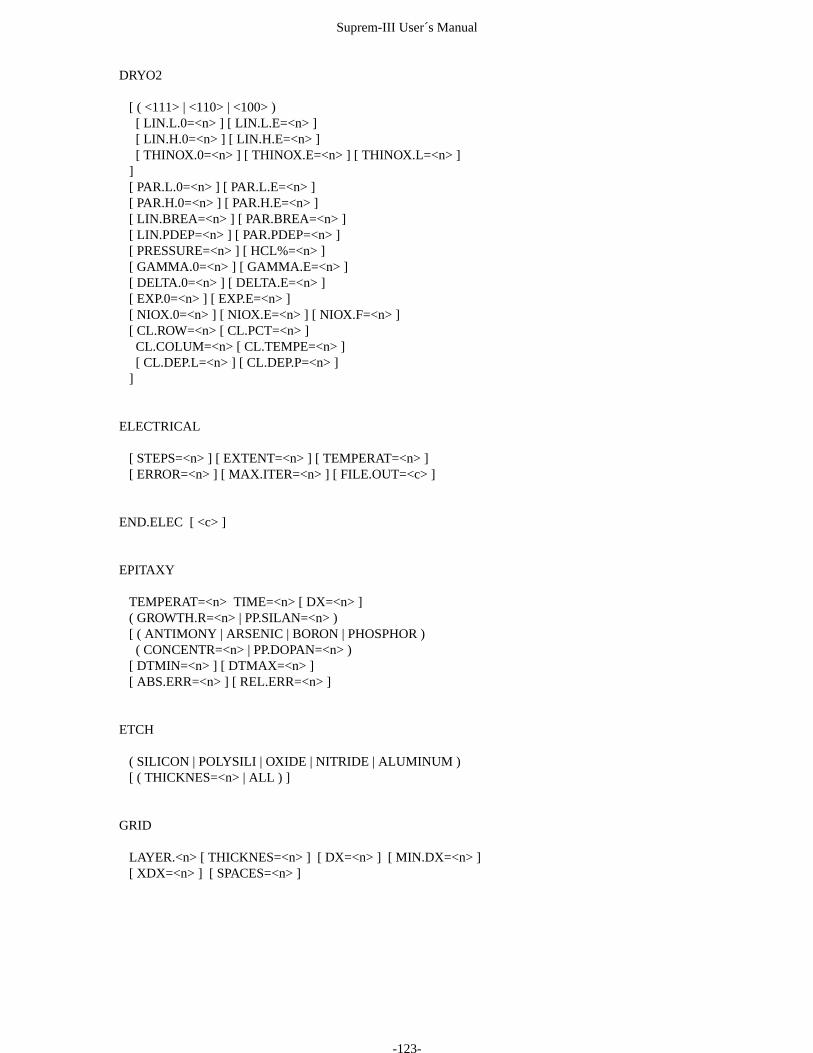
Suprem-III User´s Manual
DRYO2
[ ( <111> | <110> | <100> )[ LIN.L.0=<n> ] [ LIN.L.E=<n> ][ LIN.H.0=<n> ] [ LIN.H.E=<n> ][ THINOX.0=<n> ] [ THINOX.E=<n> ] [ THINOX.L=<n> ]
][ PAR.L.0=<n> ] [ PAR.L.E=<n> ][ PAR.H.0=<n> ] [ PAR.H.E=<n> ][ LIN.BREA=<n> ] [ PAR.BREA=<n> ][ LIN.PDEP=<n> ] [ PAR.PDEP=<n> ][ PRESSURE=<n> ] [ HCL%=<n> ][ GAMMA.0=<n> ] [ GAMMA.E=<n> ][ DELTA.0=<n> ] [ DELTA.E=<n> ][ EXP.0=<n> ] [ EXP.E=<n> ][ NIOX.0=<n> ] [ NIOX.E=<n> ] [ NIOX.F=<n> ][ CL.ROW=<n> [ CL.PCT=<n> ]CL.COLUM=<n> [ CL.TEMPE=<n> ][ CL.DEP.L=<n> ] [ CL.DEP.P=<n> ]
]
ELECTRICAL
[ STEPS=<n> ] [ EXTENT=<n> ] [ TEMPERAT=<n> ][ ERROR=<n> ] [ MAX.ITER=<n> ] [ FILE.OUT=<c> ]
END.ELEC [ <c> ]
EPITAXY
TEMPERAT=<n> TIME=<n> [ DX=<n> ]( GRO WTH.R=<n> | PP.SILAN=<n> )[ ( ANTIMONY | ARSENIC | BORON | PHOSPHOR )( CONCENTR=<n> | PP.DOPAN=<n> )
[ DTMIN=<n> ] [ DTMAX=<n> ][ ABS.ERR=<n> ] [ REL.ERR=<n> ]
ETCH
( SILICON | POLYSILI | OXIDE | NITRIDE | ALUMINUM )[ ( THICKNES=<n> | ALL ) ]
GRID
LAYER.<n> [ THICKNES=<n> ] [ DX=<n> ] [ MIN.DX=<n> ][ XDX=<n> ] [ SPA CES=<n> ]
-123-

Suprem-III User´s Manual
IMPLANT
DOSE=<n> ENERGY=<n>( ANTIMONY | ARSENIC | BF2 | BORON | PHOSPHOR )( GAUSSIAN| 2-GAUSSI| PEARSON| ( BOLTZMAN [ MINSTEPS=<n> ] [ AT.WT=<n> ] [ AT.NUMB=<n> ] ))
IMPURITY
INDEX=<n>[ NAME=<c> ] [ (DONOR | ACCEPTOR) ][ AT.WT=<n> ] [ AT.NUMB=<n> ][ IONFILE1=<c> ] [ IONFILE2=<c> ][ ( ( SILICON
[ FII.0=<n> ] [ FII.E=<n> ][ K.MF=<n> ] [ K.A=<n> ] [ K.P=<n> ]
[ MISFITST=<n> ] [ CD=<n> ][ MSF111FA=<n> ] [ MSF110FA=<n> ] [ MSF100FA=<n> ][ DAMAGEST=<n> ][ NE.0=<n> ] [ NE.E=<n> ][ ( IMPLANT | CHEMICAL )[ CTN.0=<n> ] [ CTN.E=<n> ] [ CTN.F=<n> ]
])
| ( POLYSILI[ ENTROPY=<n> ] [ HEAT.SEG=<n> ] [ Q.SITES=<n> ][ FII.0=<n> ] [ FII.E=<n> ][ ( IMPLANT | CHEMICAL )
[ CTN.0=<n> ] [ CTN.E=<n> ] [ CTN.F=<n> ]]
)| ( OXIDE | NITRIDE | ALUMINUM )[ ELECT.ST=<n> ][ DIX.0=<n> ] [ DIX.E=<n> ][ DIM.0=<n> ] [ DIM.E=<n> ][ DIMM.0=<n> ] [ DIMM.E=<n> ][ DIP.0=<n> ] [ DIP.E=<n> ]
]
-124-

Suprem-III User´s Manual
INITIALIZE
[ ( COEFFICI=<c> | FIRSTIME ) ][ STRUCTUR=<c> ] [ MIN.DX=<n> ] [ SAVESTEP ][ THICKNES=<n> ] [ DX=<n> ] [ XDX=<n> ] [ SPACES=<n> ][ ( SILICON ( <111> | <110> | <100> )
| POLYSILI( GRAINSIZ=<n> | ( TEMPERAT=<n> [ PRESSURE=<n> ] ) )
| OXIDE| NITRIDE| ALUMINUM)[ CONCENTR=<n>( ANTIMONY | ARSENIC | BORON | PHOSPHOR )
]]
LOADFILE
FILENAME=<c> ( ALL | COEFFICI | STRUCTUR )[ FORMATTE ]
PLOT
[ ACTIVE ] [ CHEMICAL ] [ TOTAL ] [ NET ][ ANTIMONY ] [ ARSENIC ] [ BORON ] [ PHOSPHOR ][ XMIN=<n> ] [ XMAX=<n> ] [ CMIN=<n> ] [ CMAX=<n> ][ LINES/PA=<n> ] [ COLUMNS=<n> ]
-125-

Suprem-III User´s Manual
MATERIAL
[ INDEX=<n> ][ NAME=<c> ] [ DX.DEFAU=<n> ][ ( SEMICOND | CONDUCTO | INSULATO ) ][ SPECIES=<n> ] [ DENSITY=<n> ][ AT.WT.1=<n> ] [ AT.WT.2=<n> ] [ AT.WT.3=<n> ][ AT.NUM.1=<n> ] [ AT.NUM.2=<n> ] [ AT.NUM.3=<n> ][ ABUND.1=<n> ] [ ABUND.2=<n> ] [ ABUND.3=<n> ][ DIFX.0=<n> ] [ DIFX.E=<n> ][ DIMX.0=<n> ] [ DIFM.E=<n> ][ DIMMX.0=<n> ] [ DIFMM.E=<n> ][ DIFP.0=<n> ] [ DIFP.E=<n> ][ NI.0=<n> ] [ NI.E=<n> ] [ NI.F=<n> ] [ DEFECTLN=<n> ][ OEDK.0=<n> ] [ OEDK.E=<n> ] [ OED.RATE=<n> ][ 100.OEDF=<n> ] [ 110.OEDF=<n> ] [ 111.OEDF=<n> ][ GSZ.H.0=<n> ] [ GSZ.H.E=<n> ][ GSZ.L.0=<n> ] [ GSZ.L.E=<n> ][ MIN.GRAI=<n> ] [ TEMP.BRE=<n> ][ RATIO.0=<n> ] [ RATIO.E=<n> ][ GEO.FACT=<n> ] [ GBE.0=<n> ] [ GBE.E=<n> ][ TAU.0=<n> ] [ TAU.E=<n> ][ AFFINITY=<n> ] [ WORK.FUN=<n> ] [ EPSILONF=<n> ][ N.VALENC=<n> ] [ N.CONDUC=<n> ] [ BAND.GAP=<n> ][ K.M=<n> ]
NITRIDE
[ NAME=<c> ] [ DX.DEFAU=<n> ][ INSULATO ][ SPECIES=<n> ] [ DENSITY=<n> ][ AT.WT.1=<n> ] [ AT.WT.2=<n> ][ AT.NUM.1=<n> ] [ AT.NUM.2=<n> ][ ABUND.1=<n> ] [ ABUND.2=<n> ][ EPSILONF=<n> ]
-126-

Suprem-III User´s Manual
NITROGEN
[ ( <111> | <110> | <100> )[ LIN.L.0=<n> ] [ LIN.L.E=<n> ][ LIN.H.0=<n> ] [ LIN.H.E=<n> ][ THINOX.0=<n> ] [ THINOX.E=<n> ] [ THINOX.L=<n> ]
][ PAR.L.0=<n> ] [ PAR.L.E=<n> ][ PAR.H.0=<n> ] [ PAR.H.E=<n> ][ LIN.BREA=<n> ] [ PAR.BREA=<n> ][ LIN.PDEP=<n> ] [ PAR.PDEP=<n> ][ PRESSURE=<n> ] [ HCL%=<n> ][ GAMMA.0=<n> ] [ GAMMA.E=<n> ][ DELTA.0=<n> ] [ DELTA.E=<n> ][ EXP.0=<n> ] [ EXP.E=<n> ][ NIOX.0=<n> ] [ NIOX.E=<n> ] [ NIOX.F=<n> ][ CL.ROW=<n> [ CL.PCT=<n> ]CL.COLUM=<n> [ CL.TEMPE=<n> ][ CL.DEP.L=<n> ] [ CL.DEP.P=<n> ]
]
OXIDE
[ NAME=<c> ] [ DX.DEFAU=<n> ][ INSULATO ][ SPECIES=<n> ] [ DENSITY=<n> ][ AT.WT.1=<n> ] [ AT.WT.2=<n> ][ AT.NUM.1=<n> ] [ AT.NUM.2=<n> ][ ABUND.1=<n> ] [ ABUND.2=<n> ][ EPSILONF=<n> ]
-127-

Suprem-III User´s Manual
PHOSPHOR
[ NAME=<c> ] [ DONOR ][ AT.WT=<n> ] [ AT.NUMB=<n> ][ IONFILE1=<c> ] [ IONFILE2=<c> ][ ( ( SILICON
[ FII.0=<n> ] [ FII.E=<n> ][ K.MF=<n> ] [ K.A=<n> ] [ K.P=<n> ]
[ MISFITST=<n> ] [ CD=<n> ][ MSF111FA=<n> ] [ MSF110FA=<n> ] [ MSF100FA=<n> ][ DAMAGEST=<n> ][ NE.0=<n> ] [ NE.E=<n> ][ ( IMPLANT | CHEMICAL )[ CTN.0=<n> ] [ CTN.E=<n> ] [ CTN.F=<n> ]
])
| ( POLYSILI[ ENTROPY=<n> ] [ HEAT.SEG=<n> ] [ Q.SITES=<n> ][ FII.0=<n> ] [ FII.E=<n> ][ ( IMPLANT | CHEMICAL )
[ CTN.0=<n> ] [ CTN.E=<n> ] [ CTN.F=<n> ]]
)| ( OXIDE | NITRIDE | ALUMINUM )[ ELECT.ST=<n> ][ DIX.0=<n> ] [ DIX.E=<n> ][ DIM.0=<n> ] [ DIM.E=<n> ][ DIMM.0=<n> ] [ DIMM.E=<n> ]
]
PLOT
[ ACTIVE ] [ CHEMICAL ] [ TOTAL ] [ NET ][ ANTIMONY ] [ ARSENIC ] [ BORON ] [ PHOSPHOR ][ XMIN=<n> ] [ XMAX=<n> ] [ CMIN=<n> ] [ CMAX=<n> ][ LAYER1 ] [ LAYER2 ] ... [ LAYER10 ][ CLEAR ] [ AXIS ] [ LINETYPE=<n> ]
[ TITLE=<c> ] [ LABEL=<c> ][ XPWIDTH=<n> ] [ YPWIDTH=<n> ][ XOFFSET=<n> ] [ YOFFSET=<n> ][ DEVICE=<c> ] [ FILENAME=<c> ]
-128-

Suprem-III User´s Manual
POLYSILI
[ NAME=<c> ] [ DX.DEFAU=<n> ][ SEMICOND ][ SPECIES=<n> ] [ DENSITY=<n> ][ AT.WT.1=<n> ] [ AT.NUM.1=<n> ] [ ABUND.1=<n> ][ DIFX.0=<n> ] [ DIFX.E=<n> ][ DIMX.0=<n> ] [ DIFM.E=<n> ][ DIMMX.0=<n> ] [ DIFMM.E=<n> ][ DIFP.0=<n> ] [ DIFP.E=<n> ][ NI.0=<n> ] [ NI.E=<n> ] [ NI.F=<n> ] [ DEFECTLN=<n> ][ OEDK.0=<n> ] [ OEDK.E=<n> ] [ OED.RATE=<n> ][ GSZ.H.0=<n> ] [ GSZ.H.E=<n> ][ GSZ.L.0=<n> ] [ GSZ.L.E=<n> ][ MIN.GRAI=<n> ] [ TEMP.BRE=<n> ][ RATIO.0=<n> ] [ RATIO.E=<n> ][ GEO.FACT=<n> ] [ GBE.0=<n> ] [ GBE.E=<n> ][ TAU.0=<n> ] [ TAU.E=<n> ][ AFFINITY=<n> ] [ EPSILONF=<n> ][ N.VALENC=<n> ] [ N.CONDUC=<n> ] [ BAND.GAP=<n> ]
[ CONCENTR[ ACTIVE ] [ CHEMICAL ] [ ALL ] [ TOTAL ] [ NET ][ ANTIMONY ] [ ARSENIC ] [ BORON ] [ PHOSPHOR ][ XMIN=<n> ] [ XMAX=<n> ]
][ IMPURITY
[ ALL| ( ANTIMONY | ARSENIC | BORON | PHOSPHOR )]
][ MATERIAL
[ ALL| ( SILICON | POLYSILI | OXIDE | NITRIDE | ALUMINUM )]
][ LAYERS ] [ SEGREGAT ] [ OXIDATIO ][ LINES/PA=<n> ] [ COLUMNS=<n> ][ LU=<n> | FILENAME=<c> ]
PROFILE
FILE=<c> CONC.COL=<n> X.COL=<n> [ LAYER=<n> ][ SKIP=<n> ] [ COUNT=<n> ] [ COM.CHAR=<c> ]
( ANTIMONY | ARSENIC | BORON | PHOSPHOR )
-129-

Suprem-III User´s Manual
RESISTIVITY
FILE=<c> CONC.COL=<n> RES.COL=<n>[ SKIP=<n> ] [ COUNT=<n> ] [ COM.CHAR=<c> ]
( ANTIMONY | ARSENIC | BORON | PHOSPHOR )( ALUMINUM | NITRIDE | OXIDE | POLYSILICON | SILICON )
SAVEFILE
FILENAME=<c> ( ALL | COEFFICI | STRUCTUR | EXPORT )[ FORMATTE ]
SEGREGAT
( ( SILICON[ 100.FACT=<n> ] [ 110.FACT=<n> ] [ 111.FACT=<n> ]
)| OXIDE | POLYSILI | NITRIDE | ALUMINUM | AIR)( ( /SILICON
[ 100.FACT=<n> ] [ 110.FACT=<n> ] [ 111.FACT=<n> ])
| /OXIDE | /POLYSIL | /NITRIDE | /ALUMINU | /AIR)( ANTIMONY | ARSENIC | BORON | PHOSPHOR )[ SEG.0=<n> ] [ SEG.E=<n> ][ TRANS.0=<n> ] [ TRANS.E=<n> ]
[ MAX.0=<n> ] [ MAX.E=<n> ][ ( MODEL.1 | MODEL.2 ) ]
[ MUI.0=<n> ] [ MUI.E=<n> ][ GRATE.0=<n> ] [ GRATE.E=<n> ][ C.INIT=<n> ] [ C.THRESH=<n> ] [ L.THICK=<n> ]
SILICON
[ NAME=<c> ] [ DX.DEFAU=<n> ][ SEMICOND ][ SPECIES=<n> ] [ DENSITY=<n> ][ AT.WT.1=<n> ] [ AT.NUM.1=<n> ] [ ABUND.1=<n> ][ NI.0=<n> ] [ NI.E=<n> ] [ NI.F=<n> ] [ DEFECTLN=<n> ][ OEDK.0=<n> ] [ OEDK.E=<n> ] [ OED.RATE=<n> ][ 100.OEDF=<n> ] [ 110.OEDF=<n> ] [ 111.OEDF=<n> ][ AFFINITY=<n> ] [ EPSILONF=<n> ][ N.VALENC=<n> ] [ N.CONDUC=<n> ] [ BAND.GAP=<n> ][ K.M=<n> ]
SOLUBILITY
FILE=<c> CONC.COL=<n> TEMP.COL=<n>[ SKIP=<n> ] [ COUNT=<n> ] [ COM.CHAR=<c> ]
( ANTIMONY | ARSENIC | BORON | PHOSPHOR )( ALUMINUM | NITRIDE | OXIDE | POLYSILICON | SILICON )
-130-
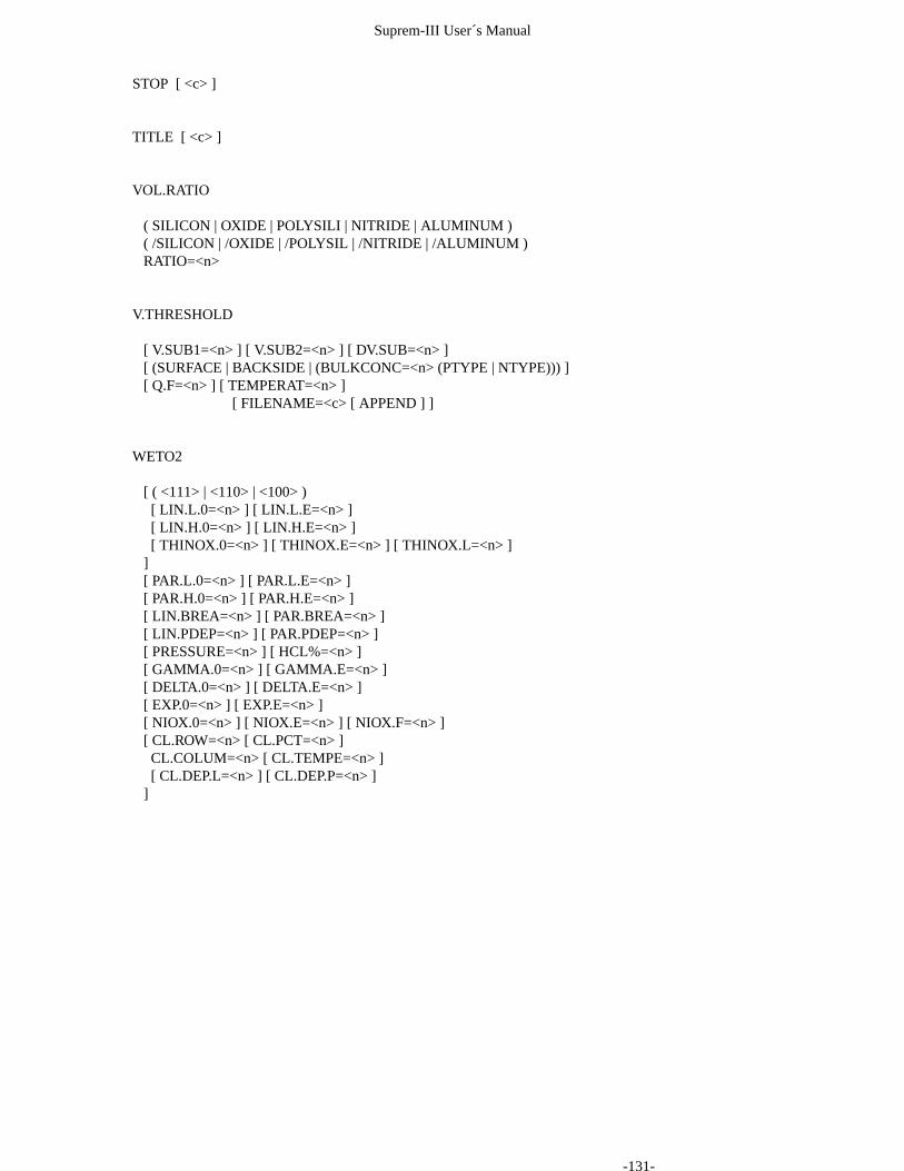
Suprem-III User´s Manual
STOP [ <c> ]
TITLE [ <c> ]
VOL.RATIO
( SILICON | OXIDE | POLYSILI | NITRIDE | ALUMINUM )( /SILICON | /OXIDE | /POLYSIL | /NITRIDE | /ALUMINUM )RATIO=<n>
V.THRESHOLD
[ V.SUB1=<n> ] [ V.SUB2=<n> ] [ DV.SUB=<n> ][ (SURFACE | BACKSIDE | (BULKCONC=<n> (PTYPE | NTYPE))) ][ Q.F=<n> ] [ TEMPERAT=<n> ]
[ FILENAME=<c> [ APPEND ] ]
WETO2
[ ( <111> | <110> | <100> )[ LIN.L.0=<n> ] [ LIN.L.E=<n> ][ LIN.H.0=<n> ] [ LIN.H.E=<n> ][ THINOX.0=<n> ] [ THINOX.E=<n> ] [ THINOX.L=<n> ]
][ PAR.L.0=<n> ] [ PAR.L.E=<n> ][ PAR.H.0=<n> ] [ PAR.H.E=<n> ][ LIN.BREA=<n> ] [ PAR.BREA=<n> ][ LIN.PDEP=<n> ] [ PAR.PDEP=<n> ][ PRESSURE=<n> ] [ HCL%=<n> ][ GAMMA.0=<n> ] [ GAMMA.E=<n> ][ DELTA.0=<n> ] [ DELTA.E=<n> ][ EXP.0=<n> ] [ EXP.E=<n> ][ NIOX.0=<n> ] [ NIOX.E=<n> ] [ NIOX.F=<n> ][ CL.ROW=<n> [ CL.PCT=<n> ]CL.COLUM=<n> [ CL.TEMPE=<n> ][ CL.DEP.L=<n> ] [ CL.DEP.P=<n> ]
]
-131-
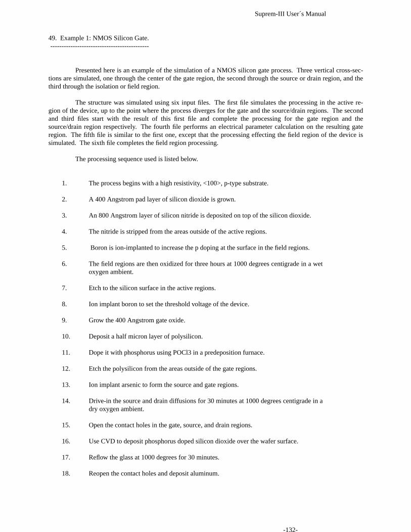
Suprem-III User´s Manual
49. Example 1: NMOS Silicon Gate.--------------------------------------------
Presented here is an example of the simulation of a NMOS silicon gate process. Three vertical cross-sec-tions are simulated, one through the center of the gate region, the second through the source or drain region, and thethird through the isolation or field region.
The structure was simulated using six input files. The first file simulates the processing in the active re-gion of the device, up to the point where the process diverges for the gate and the source/drain regions. The secondand third files start with the result of this first file and complete the processing for the gate region and thesource/drain region respectively. The fourth file performs an electrical parameter calculation on the resulting gateregion. The fifth file is similar to the first one, except that the processing effecting the field region of the device issimulated. The sixth file completes the field region processing.
The processing sequence used is listed below.
1. The process begins with a high resistivity, <100>, p-type substrate.
2. A 400 Angstrom pad layer of silicon dioxide is grown.
3. An 800 Angstrom layer of silicon nitride is deposited on top of the silicon dioxide.
4. The nitride is stripped from the areas outside of the active regions.
5. Boron is ion-implanted to increase the p doping at the surface in the field regions.
6. The field regions are then oxidized for three hours at 1000 degrees centigrade in a wetoxygen ambient.
7. Etch to the silicon surface in the active regions.
8. Ion implant boron to set the threshold voltage of the device.
9. Grow the 400 Angstrom gate oxide.
10. Deposit a half micron layer of polysilicon.
11. Dope it with phosphorus using POCl3 in a predeposition furnace.
12. Etch the polysilicon from the areas outside of the gate regions.
13. Ion implant arsenic to form the source and gate regions.
14. Drive-in the source and drain diffusions for 30 minutes at 1000 degrees centigrade in adry oxygen ambient.
15. Open the contact holes in the gate, source, and drain regions.
16. Use CVD to deposit phosphorus doped silicon dioxide over the wafer surface.
17. Reflow the glass at 1000 degrees for 30 minutes.
18. Reopen the contact holes and deposit aluminum.
-132-

Suprem-III User´s Manual
Cross-section of locally oxidized NMOS device simulated in this exam-ple. Simulations through both the active (channel) region and throughthe field oxide region are shown. In addition, a Poisson solutionthrough the channel region is used to extract threshold voltage.
-133-
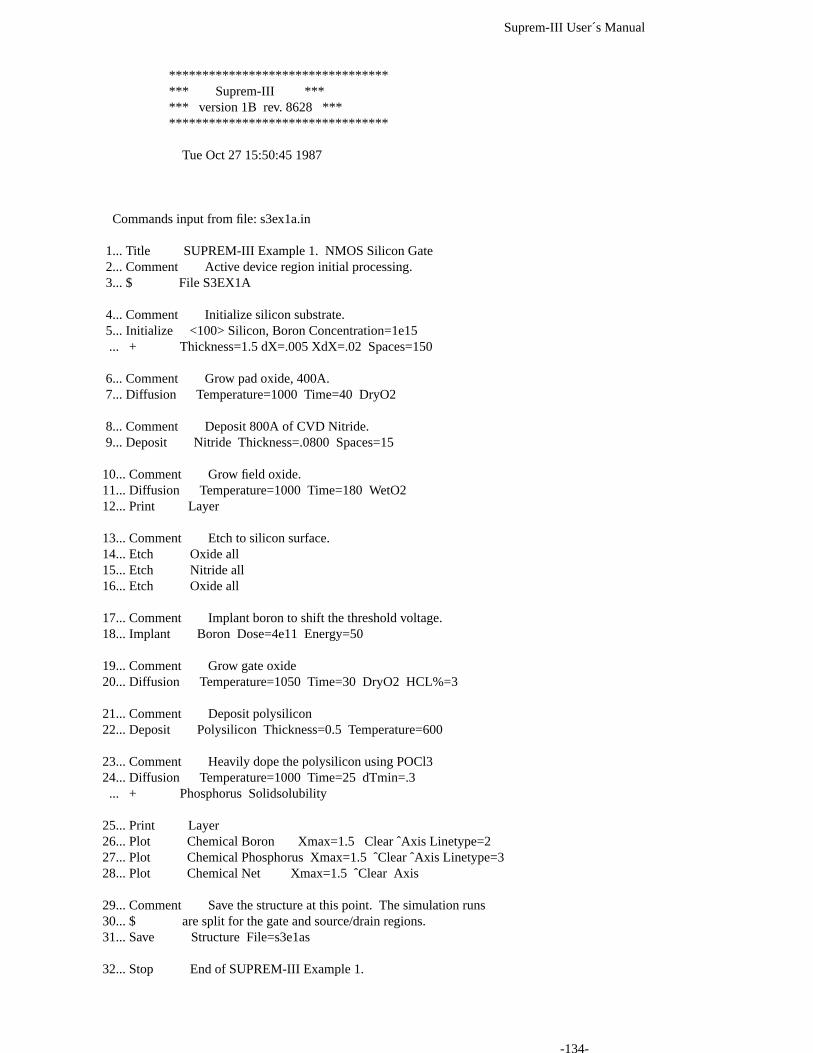
Suprem-III User´s Manual
************************************ Suprem-III ****** version 1B rev. 8628 ************************************
Tue Oct 27 15:50:45 1987
Commands input from file: s3ex1a.in
1... Title SUPREM-III Example 1. NMOS Silicon Gate2... Comment Active device region initial processing.3... $ File S3EX1A
4... Comment Initialize silicon substrate.5... Initialize <100> Silicon, Boron Concentration=1e15... + Thickness=1.5 dX=.005 XdX=.02 Spaces=150
6... Comment Grow pad oxide, 400A.7... Diffusion Temperature=1000 Time=40 DryO2
8... Comment Deposit 800A of CVD Nitride.9... Deposit Nitride Thickness=.0800 Spaces=15
10... Comment Grow field oxide.11... Diffusion Temperature=1000 Time=180 WetO212... Print Layer
13... Comment Etch to silicon surface.14... Etch Oxide all15... Etch Nitride all16... Etch Oxide all
17... Comment Implant boron to shift the threshold voltage.18... Implant Boron Dose=4e11 Energy=50
19... Comment Grow gate oxide20... Diffusion Temperature=1050 Time=30 DryO2 HCL%=3
21... Comment Deposit polysilicon22... Deposit Polysilicon Thickness=0.5 Temperature=600
23... Comment Heavily dope the polysilicon using POCl324... Diffusion Temperature=1000 Time=25 dTmin=.3... + Phosphorus Solidsolubility
25... Print Layer26... Plot Chemical Boron Xmax=1.5 Clear ˆAxis Linetype=227... Plot Chemical Phosphorus Xmax=1.5 ˆClear ˆAxis Linetype=328... Plot Chemical Net Xmax=1.5 ˆClear Axis
29... Comment Save the structure at this point. The simulation runs30... $ are split for the gate and source/drain regions.31... Save Structure File=s3e1as
32... Stop End of SUPREM-III Example 1.
-134-

Suprem-III User´s Manual
SUPREM-III Example 1. NMOS Silicon GateActive device region initial processing.File S3EX1AInitialize silicon substrate.
Grow pad oxide, 400A.
Deposit 800A of CVD Nitride.
Grow field oxide.
layer material type thickness dx dxmin top bottom orientationno. (microns) (microns) node node or grain size4 OXIDE 0.0176 0.0100 0.0010 330 3323 NITRIDE 0.0694 0.0100 0.0010 333 3472 OXIDE 0.0376 0.0100 0.0010 348 3521 SILICON 1.4835 0.0050 0.0010 353 500 <100>
Integrated Dopantlayer Net Totalno. active chemical active chemical4 0.0000e+00 0.0000e+00 0.0000e+00 0.0000e+003 0.0000e+00 -1.2524e+07 0.0000e+00 1.2524e+072 0.0000e+00 -6.8527e+09 0.0000e+00 6.8527e+091 -1.4225e+11 -1.4225e+11 1.4225e+11 1.4225e+11sum -1.4225e+11 -1.4912e+11 1.4225e+11 1.4912e+11
Integrated Dopantlayer BORONno. active chemical4 0.0000e+00 0.0000e+003 0.0000e+00 1.2524e+072 0.0000e+00 6.8527e+091 1.4225e+11 1.4225e+11sum 1.4225e+11 1.4912e+11
Junction Depths and Integrated DopantConcentrations for Each Diffused Region
layer region type junction depth net totalno. no. (microns) active Qd chemical Qd4 1 n 0.0000 0.0000e+00 0.0000e+003 2 n 0.0000 0.0000e+00 0.0000e+003 1 p 0.0694 0.0000e+00 0.0000e+002 1 p 0.0000 0.0000e+00 6.8527e+091 1 p 0.0000 1.4225e+11 1.4225e+11
Etch to silicon surface.
Implant boron to shift the threshold voltage.
Grow gate oxide
Deposit polysilicon
Heavily dope the polysilicon using POCl3
-135-

Suprem-III User´s Manual
layer material type thickness dx dxmin top bottom orientationno. (microns) (microns) node node or grain size3 POLYSILICON 0.5000 0.0100 0.0010 300 350 0.61052 OXIDE 0.0672 0.0100 0.0010 351 3581 SILICON 1.4539 0.0050 0.0010 359 500 <100>
Integrated Dopantlayer Net Totalno. active chemical active chemical3 9.6442e+15 1.6986e+16 9.6442e+15 1.6986e+162 0.0000e+00 5.3176e+12 0.0000e+00 5.5242e+121 -4.3757e+11 -4.3757e+11 4.3757e+11 4.3757e+11sum 9.6437e+15 1.6991e+16 9.6446e+15 1.6992e+16
Integrated Dopantlayer BORON PHOSPHORUSno. active chemical active chemical3 1.0440e+08 1.0440e+08 9.6442e+15 1.6986e+162 0.0000e+00 1.0328e+11 0.0000e+00 5.4209e+121 4.3757e+11 4.3757e+11 5.9474e+03 5.9474e+03sum 4.3767e+11 5.4096e+11 9.6442e+15 1.6991e+16
Junction Depths and Integrated DopantConcentrations for Each Diffused Region
layer region type junction depth net totalno. no. (microns) active Qd chemical Qd3 1 n 0.0000 9.6442e+15 1.6986e+162 2 n 0.0000 0.0000e+00 5.2968e+122 1 p 0.0242 0.0000e+00 8.0323e+101 1 p 0.0000 4.3757e+11 4.3757e+11
Save the structure at this point. The simulation runsare split for the gate and source/drain regions.
End Suprem-III
-136-
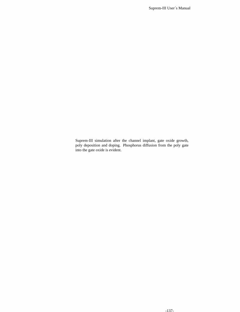
Suprem-III User´s Manual
Suprem-III simulation after the channel implant, gate oxide growth,poly deposition and doping. Phosphorus diffusion from the poly gateinto the gate oxide is evident.
-137-
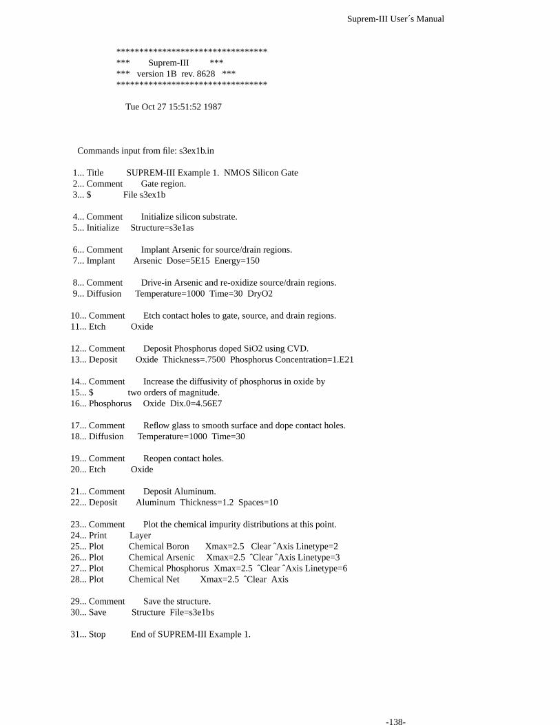
Suprem-III User´s Manual
************************************ Suprem-III ****** version 1B rev. 8628 ************************************
Tue Oct 27 15:51:52 1987
Commands input from file: s3ex1b.in
1... Title SUPREM-III Example 1. NMOS Silicon Gate2... Comment Gate region.3... $ File s3ex1b
4... Comment Initialize silicon substrate.5... Initialize Structure=s3e1as
6... Comment Implant Arsenic for source/drain regions.7... Implant Arsenic Dose=5E15 Energy=150
8... Comment Drive-in Arsenic and re-oxidize source/drain regions.9... Diffusion Temperature=1000 Time=30 DryO2
10... Comment Etch contact holes to gate, source, and drain regions.11... Etch Oxide
12... Comment Deposit Phosphorus doped SiO2 using CVD.13... Deposit Oxide Thickness=.7500 Phosphorus Concentration=1.E21
14... Comment Increase the diffusivity of phosphorus in oxide by15... $ two orders of magnitude.16... Phosphorus Oxide Dix.0=4.56E7
17... Comment Reflow glass to smooth surface and dope contact holes.18... Diffusion Temperature=1000 Time=30
19... Comment Reopen contact holes.20... Etch Oxide
21... Comment Deposit Aluminum.22... Deposit Aluminum Thickness=1.2 Spaces=10
23... Comment Plot the chemical impurity distributions at this point.24... Print Layer25... Plot Chemical Boron Xmax=2.5 Clear ˆAxis Linetype=226... Plot Chemical Arsenic Xmax=2.5 ˆClear ˆAxis Linetype=327... Plot Chemical Phosphorus Xmax=2.5 ˆClear ˆAxis Linetype=628... Plot Chemical Net Xmax=2.5 ˆClear Axis
29... Comment Save the structure.30... Save Structure File=s3e1bs
31... Stop End of SUPREM-III Example 1.
-138-
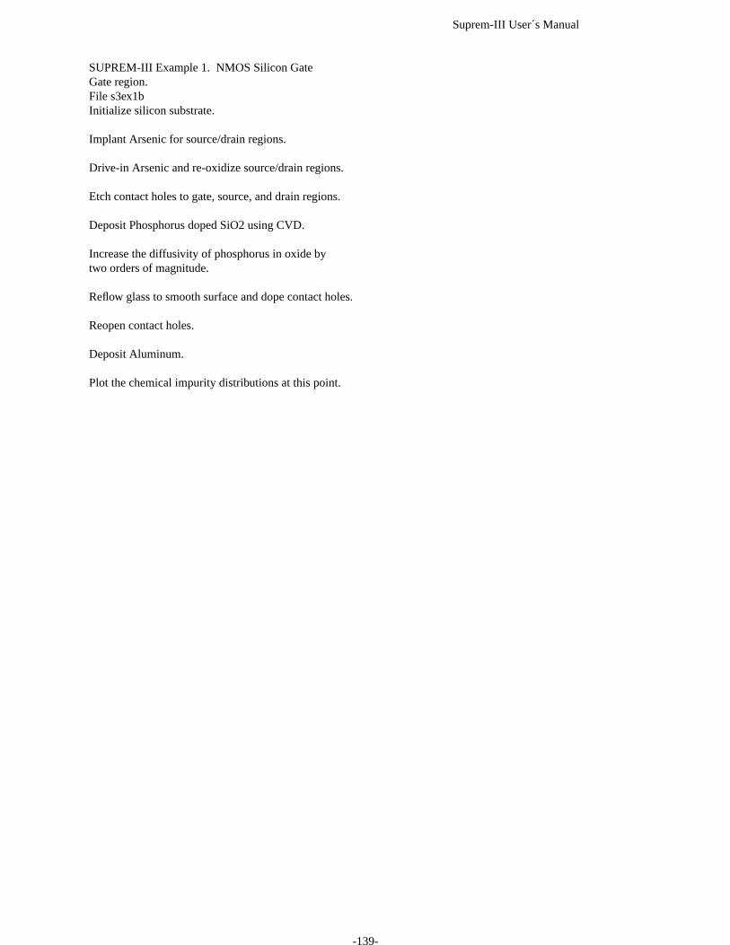
Suprem-III User´s Manual
SUPREM-III Example 1. NMOS Silicon GateGate region.File s3ex1bInitialize silicon substrate.
Implant Arsenic for source/drain regions.
Drive-in Arsenic and re-oxidize source/drain regions.
Etch contact holes to gate, source, and drain regions.
Deposit Phosphorus doped SiO2 using CVD.
Increase the diffusivity of phosphorus in oxide bytwo orders of magnitude.
Reflow glass to smooth surface and dope contact holes.
Reopen contact holes.
Deposit Aluminum.
Plot the chemical impurity distributions at this point.
-139-

Suprem-III User´s Manual
layer material type thickness dx dxmin top bottom orientationno. (microns) (microns) node node or grain size4 ALUMINUM 1.2000 0.0100 0.0010 292 3023 POLYSILICON 0.4646 0.0100 0.0010 303 350 0.90352 OXIDE 0.0672 0.0100 0.0010 351 3581 SILICON 1.4539 0.0050 0.0010 359 500 <100>
Integrated Dopantlayer Net Totalno. active chemical active chemical4 0.0000e+00 0.0000e+00 0.0000e+00 0.0000e+003 1.3770e+16 2.2278e+16 1.3770e+16 2.2278e+162 0.0000e+00 1.1498e+13 0.0000e+00 1.1705e+131 -4.3714e+11 -4.3714e+11 4.3718e+11 4.3718e+11sum 1.3770e+16 2.2289e+16 1.3771e+16 2.2290e+16
Integrated Dopantlayer PHOSPHORUS ARSENICno. active chemical active chemical4 0.0000e+00 0.0000e+00 0.0000e+00 0.0000e+003 8.9661e+15 1.7376e+16 4.8040e+15 4.9019e+152 0.0000e+00 1.0926e+13 0.0000e+00 6.7499e+111 2.0359e+07 2.0359e+07 1.4714e-16 1.4714e-16sum 8.9661e+15 1.7387e+16 4.8040e+15 4.9026e+15
Integrated Dopantlayer BORONno. active chemical4 0.0000e+00 0.0000e+003 3.3427e+08 3.3427e+082 0.0000e+00 1.0345e+111 4.3716e+11 4.3716e+11sum 4.3749e+11 5.4094e+11
Junction Depths and Integrated DopantConcentrations for Each Diffused Region
layer region type junction depth net totalno. no. (microns) active Qd chemical Qd4 1 n 0.0000 0.0000e+00 0.0000e+003 1 n 0.0000 1.3770e+16 2.2278e+162 2 n 0.0000 0.0000e+00 1.1631e+132 1 p 0.0465 0.0000e+00 3.6428e+101 1 p 0.0000 4.3714e+11 4.3718e+11
Save the structure.
End Suprem-III
-140-
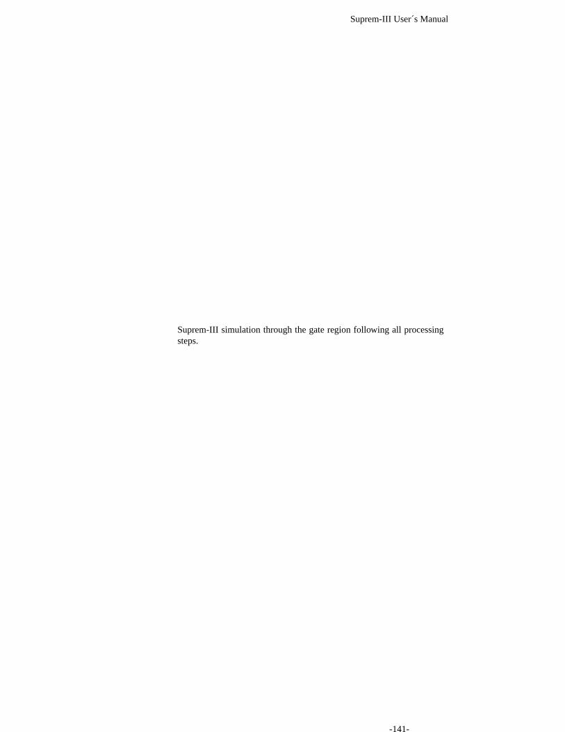
Suprem-III User´s Manual
Suprem-III simulation through the gate region following all processingsteps.
-141-

Suprem-III User´s Manual
************************************ Suprem-III ****** version 1B rev. 8628 ************************************
Tue Oct 27 15:53:35 1987
Commands input from file: s3ex1c.in
1... Title SUPREM-III Example 1. NMOS Silicon Gate2... Comment Source/drain regions.3... $ File s3ex1c
4... Comment Initialize silicon substrate.5... Initialize Structure=s3e1as
6... Comment Etch polysilicon and oxide over source/drain regions.7... Etch Polysilicon8... Etch Oxide
9... Comment Implant Arsenic for source/drain regions.10... Implant Arsenic Dose=5E15 Energy=150
11... Comment Drive-in Arsenic and re-oxidize source/drain regions.12... Diffusion Temperature=1000 Time=30 DryO2
13... Comment Etch contact holes to gate, source, and drain regions.14... Etch oxide
15... Comment Deposit Phosphorus doped SiO2 using CVD.16... Deposit Oxide Thickness=.7500 Phosphorus Concentration=1e21
17... Comment Increase the diffusivity of phosphorus in oxide by18... $ two orders of magnitude.19... Phosphorus Oxide Dix.0=4.56E7
20... Comment Reflow glass to smooth surface and dope contact holes.21... Diffusion Temperature=1000 Time=3022... Print Layer
23... Comment Reopen contact holes.24... Etch Oxide
25... Comment Deposit Aluminum.26... Deposit Aluminum Thickness=1.2 Spaces=10
27... Comment Plot the chemical impurity distributions at this point.28... Print Layer29... Plot Chemical Boron Xmax=2.5 Clear ˆAxis Linetype=230... Plot Chemical Arsenic Xmax=2.5 ˆClear ˆAxis Linetype=331... Plot Chemical Phosphorus Xmax=2.5 ˆClear ˆAxis Linetype=632... Plot Chemical Net Xmax=2.5 ˆClear Axis
33... Comment Save the structure.34... Save Structure File=s3e1cs
35... Stop End of SUPREM-III Example 1.
-142-

Suprem-III User´s Manual
SUPREM-III Example 1. NMOS Silicon GateSource/drain regions.File s3ex1cInitialize silicon substrate.
Etch polysilicon and oxide over source/drain regions.
Implant Arsenic for source/drain regions.
Drive-in Arsenic and re-oxidize source/drain regions.
Etch contact holes to gate, source, and drain regions.
Deposit Phosphorus doped SiO2 using CVD.
Increase the diffusivity of phosphorus in oxide bytwo orders of magnitude.
Reflow glass to smooth surface and dope contact holes.
layer material type thickness dx dxmin top bottom orientationno. (microns) (microns) node node or grain size2 OXIDE 0.7500 0.0100 0.0010 287 3621 SILICON 1.4282 0.0050 0.0010 363 500 <100>
Integrated Dopantlayer Net Totalno. active chemical active chemical2 0.0000e+00 7.3653e+16 0.0000e+00 7.3654e+161 5.4178e+15 5.5214e+15 5.4184e+15 5.5221e+15sum 5.4178e+15 7.9175e+16 5.4184e+15 7.9176e+16
Integrated Dopantlayer PHOSPHORUS ARSENICno. active chemical active chemical2 0.0000e+00 7.3653e+16 0.0000e+00 9.5986e+111 6.2501e+14 6.7332e+14 4.7931e+15 4.8484e+15sum 6.2501e+14 7.4326e+16 4.7931e+15 4.8494e+15
Integrated Dopantlayer BORONno. active chemical2 0.0000e+00 2.1491e+101 3.2537e+11 3.2537e+11sum 3.2537e+11 3.4686e+11
Junction Depths and Integrated DopantConcentrations for Each Diffused Region
layer region type junction depth net totalno. no. (microns) active Qd chemical Qd2 1 n 0.0000 0.0000e+00 7.3653e+161 2 n 0.0000 5.4178e+15 5.5220e+151 1 p 1.2072 1.8688e+10 3.0137e+10
Reopen contact holes.
Deposit Aluminum.
Plot the chemical impurity distributions at this point.
-143-
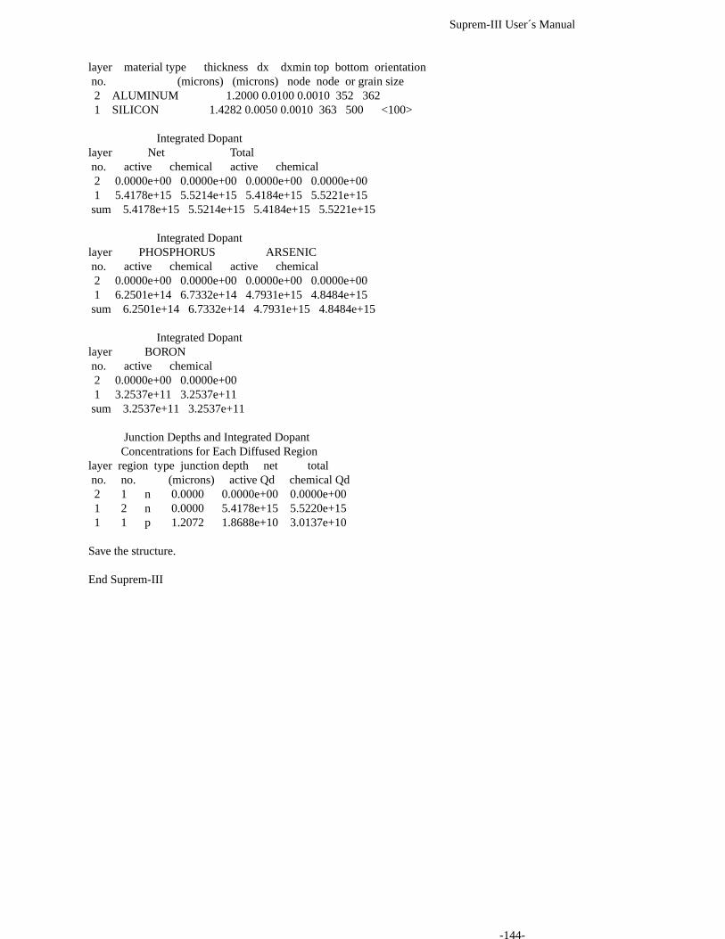
Suprem-III User´s Manual
layer material type thickness dx dxmin top bottom orientationno. (microns) (microns) node node or grain size2 ALUMINUM 1.2000 0.0100 0.0010 352 3621 SILICON 1.4282 0.0050 0.0010 363 500 <100>
Integrated Dopantlayer Net Totalno. active chemical active chemical2 0.0000e+00 0.0000e+00 0.0000e+00 0.0000e+001 5.4178e+15 5.5214e+15 5.4184e+15 5.5221e+15sum 5.4178e+15 5.5214e+15 5.4184e+15 5.5221e+15
Integrated Dopantlayer PHOSPHORUS ARSENICno. active chemical active chemical2 0.0000e+00 0.0000e+00 0.0000e+00 0.0000e+001 6.2501e+14 6.7332e+14 4.7931e+15 4.8484e+15sum 6.2501e+14 6.7332e+14 4.7931e+15 4.8484e+15
Integrated Dopantlayer BORONno. active chemical2 0.0000e+00 0.0000e+001 3.2537e+11 3.2537e+11sum 3.2537e+11 3.2537e+11
Junction Depths and Integrated DopantConcentrations for Each Diffused Region
layer region type junction depth net totalno. no. (microns) active Qd chemical Qd2 1 n 0.0000 0.0000e+00 0.0000e+001 2 n 0.0000 5.4178e+15 5.5220e+151 1 p 1.2072 1.8688e+10 3.0137e+10
Save the structure.
End Suprem-III
-144-

Suprem-III User´s Manual
Suprem-III simulation through the source-drain region following allprocessing steps.
-145-

Suprem-III User´s Manual
************************************ Suprem-III ****** version 1B rev. 8628 ************************************
Tue Oct 27 15:55:28 1987
Commands input from file: s3ex1d.in
1... Title SUPREM-III Example 1. NMOS Silicon Gate2... Comment Gate region electrical simulation.3... $ File s3ex1d
4... Comment Initialize using gate region result.5... Initialize Structure=s3e1bs
6... Comment Solve Poisson’s equation with the gate biased from7... $ 0. volts to 3. volts in .2 volt steps.8... Electrical Steps=169... Bias Layer=3 Diffusion=1 V.Majority=0. dV.Majority=.210... End
11... Stop End of SUPREM-III Example 1.
-146-

Suprem-III User´s Manual
SUPREM-III Example 1. NMOS Silicon GateGate region electrical simulation.File s3ex1dInitialize using gate region result.
Solve Poisson’s equation with the gate biased from0. volts to 3. volts in .2 volt steps.
Required Iterations = 6
Step Layer Region Concentration Conductivity SheetHoles Electrons Holes Electrons Resistivity
1 3 1 0.000e+00 2.059e+16 0.000e+00 9.840e-21 2.187e+241 1 1 2.378e+11 1.393e+06 1.263e-01 1.393e-06 5.444e+04
Required Iterations = 7
Step Layer Region Concentration Conductivity SheetHoles Electrons Holes Electrons Resistivity
2 3 1 0.000e+00 2.059e+16 0.000e+00 9.839e-21 2.188e+242 1 1 2.127e+11 1.340e+08 1.136e-01 1.324e-04 6.048e+04
Required Iterations = 19
Step Layer Region Concentration Conductivity SheetHoles Electrons Holes Electrons Resistivity
3 3 1 0.000e+00 2.058e+16 0.000e+00 9.838e-21 2.188e+243 1 1 1.925e+11 8.728e+09 1.032e-01 8.557e-03 6.156e+04
Required Iterations = 24
Step Layer Region Concentration Conductivity SheetHoles Electrons Holes Electrons Resistivity
4 3 1 0.000e+00 2.058e+16 0.000e+00 9.837e-21 2.188e+244 1 1 1.851e+11 5.019e+10 9.928e-02 4.901e-02 4.638e+04
Required Iterations = 24
Step Layer Region Concentration Conductivity SheetHoles Electrons Holes Electrons Resistivity
5 3 1 0.000e+00 2.058e+16 0.000e+00 9.836e-21 2.188e+245 1 1 1.823e+11 1.048e+11 9.783e-02 1.021e-01 3.440e+04
Required Iterations = 24
Step Layer Region Concentration Conductivity SheetHoles Electrons Holes Electrons Resistivity
6 3 1 0.000e+00 2.058e+16 0.000e+00 9.835e-21 2.189e+246 1 1 1.808e+11 1.633e+11 9.704e-02 1.587e-01 2.690e+04
Required Iterations = 23
Step Layer Region Concentration Conductivity SheetHoles Electrons Holes Electrons Resistivity
7 3 1 0.000e+00 2.057e+16 0.000e+00 9.834e-21 2.189e+247 1 1 1.798e+11 2.234e+11 9.654e-02 2.168e-01 2.195e+04
-147-

Suprem-III User´s Manual
Required Iterations = 23
Step Layer Region Concentration Conductivity SheetHoles Electrons Holes Electrons Resistivity
8 3 1 0.000e+00 2.057e+16 0.000e+00 9.833e-21 2.189e+248 1 1 1.791e+11 2.845e+11 9.618e-02 2.757e-01 1.850e+04
Required Iterations = 23
Step Layer Region Concentration Conductivity SheetHoles Electrons Holes Electrons Resistivity
9 3 1 0.000e+00 2.057e+16 0.000e+00 9.832e-21 2.189e+249 1 1 1.786e+11 3.461e+11 9.591e-02 3.351e-01 1.596e+04
Required Iterations = 23
Step Layer Region Concentration Conductivity SheetHoles Electrons Holes Electrons Resistivity
10 3 1 0.000e+00 2.056e+16 0.000e+00 9.831e-21 2.189e+2410 1 1 1.782e+11 4.082e+11 9.570e-02 3.948e-01 1.402e+04
Required Iterations = 23
Step Layer Region Concentration Conductivity SheetHoles Electrons Holes Electrons Resistivity
11 3 1 0.000e+00 2.056e+16 0.000e+00 9.830e-21 2.190e+2411 1 1 1.779e+11 4.706e+11 9.552e-02 4.547e-01 1.250e+04
Required Iterations = 23
Step Layer Region Concentration Conductivity SheetHoles Electrons Holes Electrons Resistivity
12 3 1 0.000e+00 2.056e+16 0.000e+00 9.829e-21 2.190e+2412 1 1 1.776e+11 5.332e+11 9.538e-02 5.149e-01 1.127e+04
Required Iterations = 23
Step Layer Region Concentration Conductivity SheetHoles Electrons Holes Electrons Resistivity
13 3 1 0.000e+00 2.056e+16 0.000e+00 9.828e-21 2.190e+2413 1 1 1.774e+11 5.960e+11 9.526e-02 5.751e-01 1.026e+04
Required Iterations = 23
Step Layer Region Concentration Conductivity SheetHoles Electrons Holes Electrons Resistivity
14 3 1 0.000e+00 2.055e+16 0.000e+00 9.827e-21 2.190e+2414 1 1 1.772e+11 6.589e+11 9.516e-02 6.355e-01 9.413e+03
Required Iterations = 24
Step Layer Region Concentration Conductivity SheetHoles Electrons Holes Electrons Resistivity
15 3 1 0.000e+00 2.055e+16 0.000e+00 9.826e-21 2.191e+2415 1 1 1.770e+11 7.219e+11 9.506e-02 6.960e-01 8.695e+03
-148-
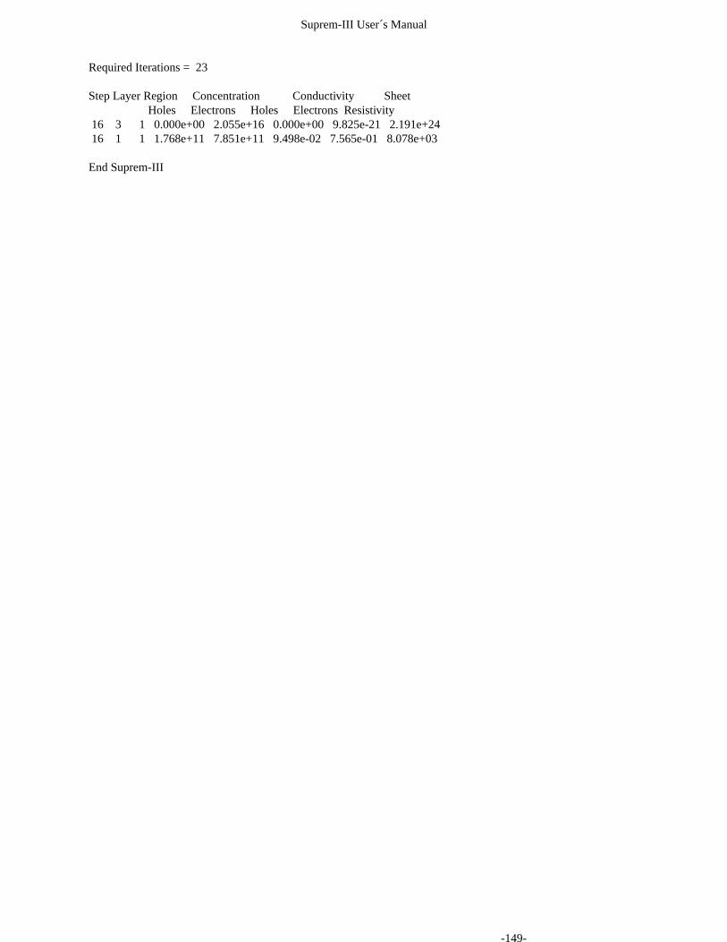
Suprem-III User´s Manual
Required Iterations = 23
Step Layer Region Concentration Conductivity SheetHoles Electrons Holes Electrons Resistivity
16 3 1 0.000e+00 2.055e+16 0.000e+00 9.825e-21 2.191e+2416 1 1 1.768e+11 7.851e+11 9.498e-02 7.565e-01 8.078e+03
End Suprem-III
-149-
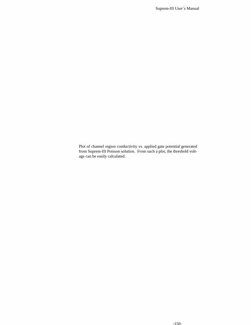
Suprem-III User´s Manual
Plot of channel region conductivity vs. applied gate potential generatedfrom Suprem-III Poisson solution. From such a plot, the threshold volt-age can be easily calculated.
-150-
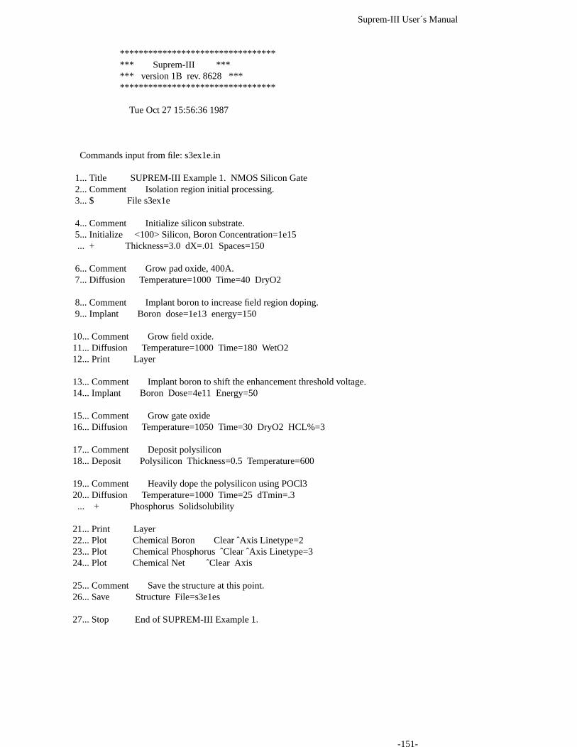
Suprem-III User´s Manual
************************************ Suprem-III ****** version 1B rev. 8628 ************************************
Tue Oct 27 15:56:36 1987
Commands input from file: s3ex1e.in
1... Title SUPREM-III Example 1. NMOS Silicon Gate2... Comment Isolation region initial processing.3... $ File s3ex1e
4... Comment Initialize silicon substrate.5... Initialize <100> Silicon, Boron Concentration=1e15... + Thickness=3.0 dX=.01 Spaces=150
6... Comment Grow pad oxide, 400A.7... Diffusion Temperature=1000 Time=40 DryO2
8... Comment Implant boron to increase field region doping.9... Implant Boron dose=1e13 energy=150
10... Comment Grow field oxide.11... Diffusion Temperature=1000 Time=180 WetO212... Print Layer
13... Comment Implant boron to shift the enhancement threshold voltage.14... Implant Boron Dose=4e11 Energy=50
15... Comment Grow gate oxide16... Diffusion Temperature=1050 Time=30 DryO2 HCL%=3
17... Comment Deposit polysilicon18... Deposit Polysilicon Thickness=0.5 Temperature=600
19... Comment Heavily dope the polysilicon using POCl320... Diffusion Temperature=1000 Time=25 dTmin=.3... + Phosphorus Solidsolubility
21... Print Layer22... Plot Chemical Boron Clear ˆAxis Linetype=223... Plot Chemical Phosphorus ˆClear ˆAxis Linetype=324... Plot Chemical Net ˆClear Axis
25... Comment Save the structure at this point.26... Save Structure File=s3e1es
27... Stop End of SUPREM-III Example 1.
-151-

Suprem-III User´s Manual
SUPREM-III Example 1. NMOS Silicon GateIsolation region initial processing.File s3ex1eInitialize silicon substrate.
Grow pad oxide, 400A.
Implant boron to increase field region doping.
Grow field oxide.
layer material type thickness dx dxmin top bottom orientationno. (microns) (microns) node node or grain size2 OXIDE 0.7604 0.0100 0.0010 348 3771 SILICON 2.6654 0.0100 0.0010 378 500 <100>
Integrated Dopantlayer Net Totalno. active chemical active chemical2 0.0000e+00 -6.1674e+12 0.0000e+00 6.1674e+121 -4.1330e+12 -4.1330e+12 4.1330e+12 4.1330e+12sum -4.1330e+12 -1.0300e+13 4.1330e+12 1.0300e+13
Integrated Dopantlayer BORONno. active chemical2 0.0000e+00 6.1674e+121 4.1330e+12 4.1330e+12sum 4.1330e+12 1.0300e+13
Junction Depths and Integrated DopantConcentrations for Each Diffused Region
layer region type junction depth net totalno. no. (microns) active Qd chemical Qd2 1 p 0.0000 0.0000e+00 6.1674e+121 1 p 0.0000 4.1330e+12 4.1330e+12
Implant boron to shift the enhancement threshold voltage.
Grow gate oxide
Deposit polysilicon
Heavily dope the polysilicon using POCl3
-152-

Suprem-III User´s Manual
layer material type thickness dx dxmin top bottom orientationno. (microns) (microns) node node or grain size3 POLYSILICON 0.5000 0.0100 0.0010 297 347 0.61302 OXIDE 0.7683 0.0100 0.0010 348 3771 SILICON 2.6620 0.0100 0.0010 378 500 <100>
Integrated Dopantlayer Net Totalno. active chemical active chemical3 9.6452e+15 1.7004e+16 9.6452e+15 1.7004e+162 0.0000e+00 3.6407e+12 0.0000e+00 1.6968e+131 -4.0361e+12 -4.0361e+12 4.0361e+12 4.0361e+12sum 9.6411e+15 1.7004e+16 9.6492e+15 1.7025e+16
Integrated Dopantlayer BORON PHOSPHORUSno. active chemical active chemical3 1.2793e+07 1.2793e+07 9.6452e+15 1.7004e+162 0.0000e+00 6.6638e+12 0.0000e+00 1.0305e+131 4.0361e+12 4.0361e+12 0.0000e+00 0.0000e+00sum 4.0361e+12 1.0700e+13 9.6452e+15 1.7014e+16
Junction Depths and Integrated DopantConcentrations for Each Diffused Region
layer region type junction depth net totalno. no. (microns) active Qd chemical Qd3 1 n 0.0000 9.6452e+15 1.7004e+162 2 n 0.0000 0.0000e+00 9.7384e+122 1 p 0.0430 0.0000e+00 6.6450e+121 1 p 0.0000 4.0361e+12 4.0361e+12
Save the structure at this point.
End Suprem-III
-153-
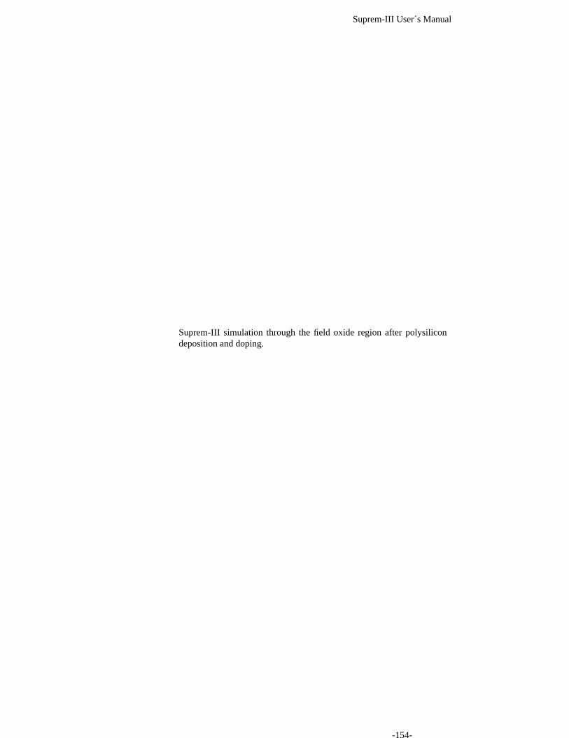
Suprem-III User´s Manual
Suprem-III simulation through the field oxide region after polysilicondeposition and doping.
-154-

Suprem-III User´s Manual
************************************ Suprem-III ****** version 1B rev. 8628 ************************************
Tue Oct 27 15:57:39 1987
Commands input from file: s3ex1f.in
1... Title SUPREM-III Example 1. NMOS Silicon Gate2... Comment Final isolation region processing.3... $ File s3ex1f
4... Comment Initialize silicon substrate.5... Initialize Structure=s3e1es
6... Comment Etch polysilicon and oxide over source/drain regions.7... Etch Polysilicon8... Etch Oxide Amount=.0700
9... Comment Implant Arsenic for source/drain regions.10... Implant Arsenic Dose=5E15 Energy=150
11... Comment Drive-in Arsenic and re-oxidize source/drain regions.12... Diffusion Temperature=1000 Time=30 DryO2
13... Comment Deposit Phosphorus doped SiO2 using CVD.14... Deposit Oxide Thickness=.7500 Phosphorus Concentration=1e21
15... Comment Reflow glass to smooth surface and dope contact holes.16... Diffusion Temperature=1000 Time=30
17... Comment Deposit Aluminum.18... Deposit Aluminum Thickness=1.2 Spaces=10
19... Comment Plot the chemical impurity distributions at this point.20... Print Layer21... Plot Chemical Boron Clear ˆAxis Linetype=222... Plot Chemical Arsenic ˆClear ˆAxis Linetype=323... Plot Chemical Phosphorus ˆClear ˆAxis Linetype=624... Plot Chemical Net ˆClear Axis
25... Comment Save the structure.26... Save Structure File=s3e1fs
27... Stop End of SUPREM-III Example 1.
-155-
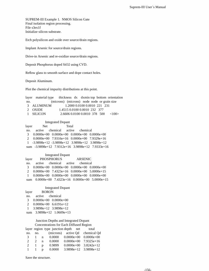
Suprem-III User´s Manual
SUPREM-III Example 1. NMOS Silicon GateFinal isolation region processing.File s3ex1fInitialize silicon substrate.
Etch polysilicon and oxide over source/drain regions.
Implant Arsenic for source/drain regions.
Drive-in Arsenic and re-oxidize source/drain regions.
Deposit Phosphorus doped SiO2 using CVD.
Reflow glass to smooth surface and dope contact holes.
Deposit Aluminum.
Plot the chemical impurity distributions at this point.
layer material type thickness dx dxmin top bottom orientationno. (microns) (microns) node node or grain size3 ALUMINUM 1.2000 0.0100 0.0010 221 2312 OXIDE 1.4515 0.0100 0.0010 232 3771 SILICON 2.6606 0.0100 0.0010 378 500 <100>
Integrated Dopantlayer Net Totalno. active chemical active chemical3 0.0000e+00 0.0000e+00 0.0000e+00 0.0000e+002 0.0000e+00 7.9316e+16 0.0000e+00 7.9329e+161 -3.9898e+12 -3.9898e+12 3.9898e+12 3.9898e+12sum -3.9898e+12 7.9312e+16 3.9898e+12 7.9333e+16
Integrated Dopantlayer PHOSPHORUS ARSENICno. active chemical active chemical3 0.0000e+00 0.0000e+00 0.0000e+00 0.0000e+002 0.0000e+00 7.4323e+16 0.0000e+00 5.0000e+151 0.0000e+00 0.0000e+00 0.0000e+00 0.0000e+00sum 0.0000e+00 7.4323e+16 0.0000e+00 5.0000e+15
Integrated Dopantlayer BORONno. active chemical3 0.0000e+00 0.0000e+002 0.0000e+00 6.6191e+121 3.9898e+12 3.9898e+12sum 3.9898e+12 1.0609e+13
Junction Depths and Integrated DopantConcentrations for Each Diffused Region
layer region type junction depth net totalno. no. (microns) active Qd chemical Qd3 1 n 0.0000 0.0000e+00 0.0000e+002 2 n 0.0000 0.0000e+00 7.9325e+162 1 p 0.9899 0.0000e+00 3.8242e+121 1 p 0.0000 3.9898e+12 3.9898e+12
Save the structure.
-156-

Suprem-III User´s Manual
End Suprem-III
-157-

Suprem-III User´s Manual
Suprem-III simulation through the field oxide region following all pro-cessing steps.
-158-
Suprem-III User´s Manual
50. Example 2: Bipolar Polysilicon Doped Emitter.--------------------------------------------------------------
Presented here is an example of the simulation of a bipolar process with a polysilicon doped emitter. Twovertical cross-sections are simulated, one through the emitter region, and other through the isolation region.
The structure was simulated using five input files. The first file simulates the processing in the active re-gion of the device up to the point of the isolation oxidation. The second file starts with the result of this first file andcompletes the processing in the active region. The third file performs an electrical parameter calculation on the re-sulting structure. As in the first example, the fourth file is similar to the first one, except that the processing in theisolation region is simulated. The fifth file completes the isolation region processing.
The processing sequence used is listed below.
1. The process begins with a high resistivity, <100>, p-type substrate.
2. Thermally oxidize the substrate, growing approximately one micron of silicon dioxide.
3. Remove the oxide layer from the areas where the buried layers are to be placed.
4. Ion implant antimony at a dose of 10ˆ15/cmˆ2. Drive in the buried layer for five hoursat 1150 degrees Centigrade.
5. Etch the silicon dioxide from the surface.
6. Epitaxial growth of 1.6 microns of arsenic doped silicon.
7. Thermally grow a 400 Angstrom pad oxide.
8. Deposit 800 Angstroms of silicon nitride.
9. Etch the nitride and oxide from the isolation regions.
10. Etch the silicon halfway through the epi-layer.
11. Ion implant boron in the field regions to increase the surface p doping. Use a dose of10ˆ13/cmˆ2 and an implant energy of 50 KeV.
12. Thermally oxidize the field regions to an oxide thickness equal to approximately one-half that of the epi-layer.
13. Strip the nitride layer.
14. Using a photoresist mask, implant the base region. Use boron at a dose of 10ˆ14/cmˆ2and an energy of 50KeV.
15. Etch the oxide from the emitter region.
16. Deposit arsenic doped polysilicon.
17. Remove the polysilicon from the non-emitter regions.
18. Anneal to drive-in the emitter and activate the base diffusion.
-159-

Suprem-III User´s Manual
Cross-section of locally oxidized bipolar structure simulated in this ex-ample. Simulations through the active (emitter-base) region andthrough the field oxide are shown. In addition, a Poisson solutionthrough the active region is used to calculate the base region sheet re-sistance as a function of collector-base voltage.
-160-

Suprem-III User´s Manual
************************************ Suprem-III ****** version 1B rev. 8628 ************************************
Tue Oct 27 16:24:46 1987
Commands input from file: s3ex2a.in
1... Title Suprem-III Example 2. Bipolar Poly doped emitter.2... $ Initial active region formation.3... $ File s3ex2a
4... $ Comment Initialize the silicon substrate.5... Initialize <100> Silicon, Boron Concentration=5e14... + Thickness=5. dX=.01 XdX=.05 Spaces=100
6... Comment Grow masking oxide for non-active regions.7... Diffusion Temperature=1150 Time=100 WetO2
8... Comment Etch the oxide over the buried layer regions.9... Etch Oxide
10... Comment Implant and drive-in the antimony buried layer.11... Implant Antimony Dose=5E14 Energy=12012... Diffusion Temperature=1150 Time=15 DryO213... Diffusion Temperature=1150 Time=30014... Print Layer15... Plot Net Chemical Xmax=5
16... Comment Etch off the oxide.17... Etch Oxide
18... Comment Grow 1.6 micron of arsenic doped epi.19... Epitaxy Temperature=1050 Time=4 Growth.Rate=.4... + Arsenic Gas.Conc=5E15
20... Comment Grow a 400A pad oxide.21... Diffusion Temperature=1060 Time=20 DryO2
22... Comment Deposit nitride to mask the field oxidation.23... Deposit Nitride Thickness=.08
24... Comment Plot the chemical impurity distributions at this point.25... Print Layer26... Plot Chemical Boron Xmax=5 Clear ˆAxis Linetype=227... Plot Chemical Arsenic Xmax=5 ˆClear ˆAxis Linetype=428... Plot Chemical Antimony Xmax=5 ˆClear ˆAxis Linetype=529... Plot Chemical Net Xmax=5 ˆClear Axis Linetype=1
30... Comment Save the simulation structure at this point for use in31... $ subsequent processing.32... Savefile Structure File=s3e2as
33... Stop
-161-

Suprem-III User´s Manual
Suprem-III Example 2. Bipolar Poly doped emitter.Initial active region formation.File s3ex2aComment Initialize the silicon substrate.
Grow masking oxide for non-active regions.
Etch the oxide over the buried layer regions.
Implant and drive-in the antimony buried layer.
layer material type thickness dx dxmin top bottom orientationno. (microns) (microns) node node or grain size2 OXIDE 0.0694 0.0100 0.0010 422 4241 SILICON 4.5443 0.0100 0.0010 425 500 <100>
Integrated Dopantlayer Net Totalno. active chemical active chemical2 0.0000e+00 7.8487e+11 0.0000e+00 7.9134e+111 4.9032e+14 4.9032e+14 4.9074e+14 4.9074e+14sum 4.9032e+14 4.9110e+14 4.9074e+14 4.9153e+14
Integrated Dopantlayer BORON ANTIMONYno. active chemical active chemical2 0.0000e+00 3.2381e+09 0.0000e+00 7.8810e+111 2.1107e+11 2.1107e+11 4.9053e+14 4.9053e+14sum 2.1107e+11 2.1430e+11 4.9053e+14 4.9131e+14
Junction Depths and Integrated DopantConcentrations for Each Diffused Region
layer region type junction depth net totalno. no. (microns) active Qd chemical Qd2 1 n 0.0000 0.0000e+00 7.9134e+111 2 n 0.0000 4.9041e+14 4.9062e+141 1 p 2.4736 9.6534e+10 1.0662e+11
Etch off the oxide.
Grow 1.6 micron of arsenic doped epi.
Grow a 400A pad oxide.
Deposit nitride to mask the field oxidation.
Plot the chemical impurity distributions at this point.
-162-

Suprem-III User´s Manual
layer material type thickness dx dxmin top bottom orientationno. (microns) (microns) node node or grain size3 NITRIDE 0.0800 0.0100 0.0010 254 2622 OXIDE 0.0406 0.0100 0.0010 263 2661 SILICON 6.1265 0.0100 0.0010 267 500 <100>
Integrated Dopantlayer Net Totalno. active chemical active chemical3 0.0000e+00 0.0000e+00 0.0000e+00 0.0000e+002 0.0000e+00 2.4201e+09 0.0000e+00 2.4201e+091 4.8995e+14 4.8995e+14 4.9037e+14 4.9037e+14sum 4.8995e+14 4.8995e+14 4.9037e+14 4.9037e+14
Integrated Dopantlayer ARSENIC ANTIMONYno. active chemical active chemical3 0.0000e+00 0.0000e+00 0.0000e+00 0.0000e+002 0.0000e+00 2.4201e+09 0.0000e+00 0.0000e+001 7.9866e+11 7.9866e+11 4.8936e+14 4.8936e+14sum 7.9866e+11 8.0108e+11 4.8936e+14 4.8936e+14
Integrated Dopantlayer BORONno. active chemical3 0.0000e+00 0.0000e+002 0.0000e+00 7.3250e-011 2.1099e+11 2.1099e+11sum 2.1099e+11 2.1099e+11
Junction Depths and Integrated DopantConcentrations for Each Diffused Region
layer region type junction depth net totalno. no. (microns) active Qd chemical Qd3 1 n 0.0000 0.0000e+00 0.0000e+002 1 n 0.0000 0.0000e+00 2.4201e+091 2 n 0.0000 4.9004e+14 4.9025e+141 1 p 4.0558 9.6256e+10 1.0673e+11
Save the simulation structure at this point for use insubsequent processing.
End Suprem-III
-163-
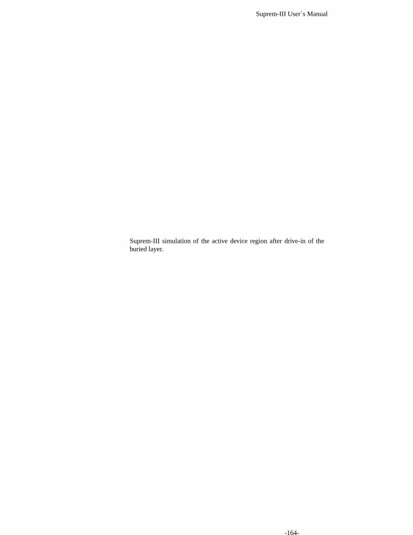
Suprem-III User´s Manual
Suprem-III simulation of the active device region after drive-in of theburied layer.
-164-

Suprem-III User´s Manual
Suprem-III simulation of the active device region after drive-in of theburied layer, epi growth, and oxide/nitride deposition.
-165-

Suprem-III User´s Manual
************************************ Suprem-III ****** version 1B rev. 8628 ************************************
Tue Oct 27 16:31:39 1987
Commands input from file: s3ex2b.in
1... Title Suprem-III Example 2. Bipolar Poly doped emitter.2... $ Final active device region formation.3... $ File s3ex2b
4... Comment Start from the result of s3ex2a.5... Initialize Structure=s3e2as
6... Comment Field oxide growth. Oxidation is masked by nitride.7... Diffusion Temperature=800 Time=30 t.rate=108... Diffusion Temperature=1000 Time=15 DryO29... Diffusion Temperature=1100 Time=210 WetO210... Diffusion Temperature=1100 Time=15 DryO211... Diffusion Temperature=1100 Time=10 t.rate=-3012... Print Layer13... Plot Net Chemical Xmax=5
14... Comment Etch the oxide and nitride layers.15... Etch Oxide16... Etch Nitride17... Etch Oxide
18... Comment Move the fine grid to the surface.19... Grid Layer.1 Xdx=0.
20... Comment Implant the boron base.21... Implant Boron Dose=1E14 Energy=50
22... Comment Remove oxide from emitter region.23... Etch Oxide
24... Comment Deposit arsenic doped polysilicon for emitter contacts.25... Deposit Polysilicon, Thickness=.5 Temperature=620... + Arsenic Concentration=1e20
26... Comment Anneal to activate base and drive-in emitter.27... Diffusion Temperature=1000 Time=20 WetO2
28... Comment Plot the electrically Active impurity distributions.29... Print Layer30... Plot Active Boron Xmax=6 Clear ˆAxis Linetype=231... Plot Active Arsenic Xmax=6 ˆClear ˆAxis Linetype=432... Plot Active Antimony Xmax=6 ˆClear ˆAxis Linetype=533... Plot Active Net Xmax=6 ˆClear Axis Linetype=1
34... Comment Save the resulting active region.35... Savefile Structure File=s3e2bs
36... Stop
-166-
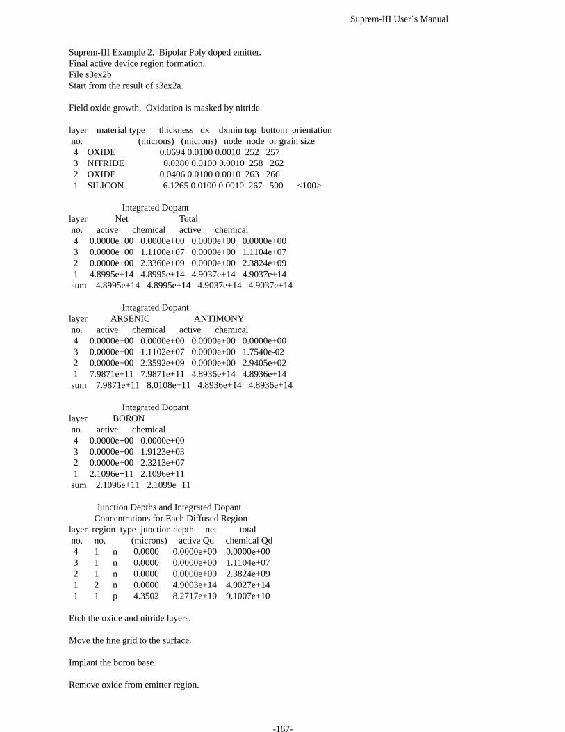
Suprem-III User´s Manual
Suprem-III Example 2. Bipolar Poly doped emitter.Final active device region formation.File s3ex2bStart from the result of s3ex2a.
Field oxide growth. Oxidation is masked by nitride.
layer material type thickness dx dxmin top bottom orientationno. (microns) (microns) node node or grain size4 OXIDE 0.0694 0.0100 0.0010 252 2573 NITRIDE 0.0380 0.0100 0.0010 258 2622 OXIDE 0.0406 0.0100 0.0010 263 2661 SILICON 6.1265 0.0100 0.0010 267 500 <100>
Integrated Dopantlayer Net Totalno. active chemical active chemical4 0.0000e+00 0.0000e+00 0.0000e+00 0.0000e+003 0.0000e+00 1.1100e+07 0.0000e+00 1.1104e+072 0.0000e+00 2.3360e+09 0.0000e+00 2.3824e+091 4.8995e+14 4.8995e+14 4.9037e+14 4.9037e+14sum 4.8995e+14 4.8995e+14 4.9037e+14 4.9037e+14
Integrated Dopantlayer ARSENIC ANTIMONYno. active chemical active chemical4 0.0000e+00 0.0000e+00 0.0000e+00 0.0000e+003 0.0000e+00 1.1102e+07 0.0000e+00 1.7540e-022 0.0000e+00 2.3592e+09 0.0000e+00 2.9405e+021 7.9871e+11 7.9871e+11 4.8936e+14 4.8936e+14sum 7.9871e+11 8.0108e+11 4.8936e+14 4.8936e+14
Integrated Dopantlayer BORONno. active chemical4 0.0000e+00 0.0000e+003 0.0000e+00 1.9123e+032 0.0000e+00 2.3213e+071 2.1096e+11 2.1096e+11sum 2.1096e+11 2.1099e+11
Junction Depths and Integrated DopantConcentrations for Each Diffused Region
layer region type junction depth net totalno. no. (microns) active Qd chemical Qd4 1 n 0.0000 0.0000e+00 0.0000e+003 1 n 0.0000 0.0000e+00 1.1104e+072 1 n 0.0000 0.0000e+00 2.3824e+091 2 n 0.0000 4.9003e+14 4.9027e+141 1 p 4.3502 8.2717e+10 9.1007e+10
Etch the oxide and nitride layers.
Move the fine grid to the surface.
Implant the boron base.
Remove oxide from emitter region.
-167-

Suprem-III User´s Manual
Error number 210 detected in line number 23The material to be etched did not match the top material.No etching occured.
Deposit arsenic doped polysilicon for emitter contacts.
Anneal to activate base and drive-in emitter.
Plot the electrically Active impurity distributions.
layer material type thickness dx dxmin top bottom orientationno. (microns) (microns) node node or grain size3 OXIDE 0.2924 0.0100 0.0010 214 2282 POLYSILICON 0.3714 0.0100 0.0010 229 266 0.54651 SILICON 6.1265 0.0100 0.0010 267 500 <100>
Integrated Dopantlayer Net Totalno. active chemical active chemical3 0.0000e+00 5.0738e+14 0.0000e+00 5.0772e+142 3.8821e+15 3.9912e+15 3.8948e+15 4.0039e+151 8.7747e+14 8.8244e+14 1.0649e+15 1.0699e+15sum 4.7596e+15 5.3811e+15 4.9597e+15 5.5815e+15
Integrated Dopantlayer ARSENIC ANTIMONYno. active chemical active chemical3 0.0000e+00 5.0755e+14 0.0000e+00 1.6316e+032 3.8884e+15 3.9976e+15 4.3948e+04 4.3948e+041 4.8182e+14 4.8680e+14 4.8936e+14 4.8936e+14sum 4.3703e+15 4.9919e+15 4.8936e+14 4.8936e+14
Integrated Dopantlayer BORONno. active chemical3 0.0000e+00 1.7080e+112 6.3257e+12 6.3257e+121 9.3716e+13 9.3716e+13sum 1.0004e+14 1.0021e+14
Junction Depths and Integrated DopantConcentrations for Each Diffused Region
layer region type junction depth net totalno. no. (microns) active Qd chemical Qd3 1 n 0.0000 0.0000e+00 5.0772e+142 1 n 0.0000 3.8821e+15 4.0039e+151 4 n 0.0000 4.6016e+14 5.0284e+141 3 p 0.1051 7.1342e+13 7.2380e+131 2 n 0.4744 4.8978e+14 4.9003e+141 1 p 4.3076 8.3108e+10 9.4636e+10
Save the resulting active region.
End Suprem-III
-168-

Suprem-III User´s Manual
Suprem-III simulation of the active device region following field oxida-tion. The Si3N4 has masked the oxidation in this region, although ithas been partially oxidized itself. The Antimony buried layer has dif-fused upward during the local oxidation process.
-169-

Suprem-III User´s Manual
Suprem-III simulation of the active device region following all process-ing steps. The original N epi layer has almost disappeared because ofburied layer and base diffusion
-170-

Suprem-III User´s Manual
************************************ Suprem-III ****** version 1B rev. 8628 ************************************
Tue Oct 27 16:36:05 1987
Commands input from file: s3ex2c.in
1... Title Suprem-III Example 2. Bipolar Poly doped emitter.2... $ Electrical simulation of the active device region.3... $ File s3ex2c.
4... Comment Start with the result of the active device region simulation.5... Initialize Structure=s3e2bs
6... Comment Solve Poisson’s equation with the collector ramped7... $ from 0 volts to 6 volts in 2 volt steps.8... Electrical Extent=3 Steps=49... Bias Layer=1 Diffusion=3 V.Minority=0 DV.Minority=210... Bias Layer=1 Diffusion=2 V.Majority=0 DV.Majority=211... Bias Layer=1 Diffusion=1 V.Minority=0 DV.Minority=212... End
13... Stop
-171-
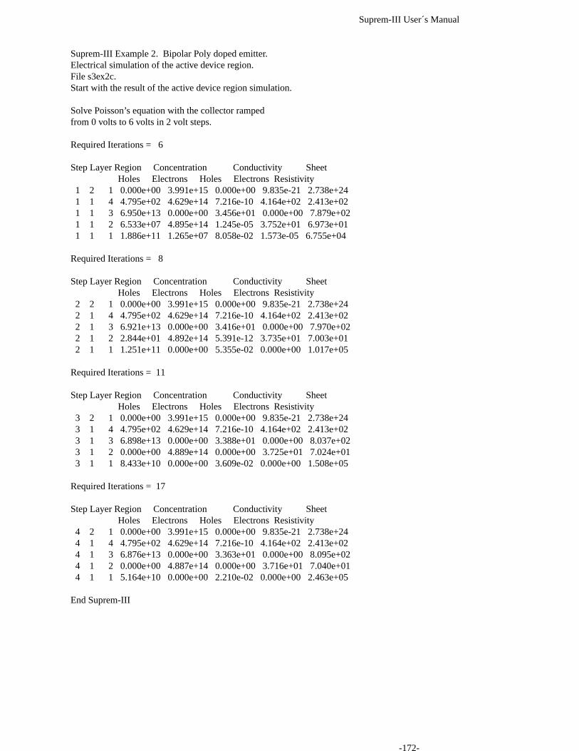
Suprem-III User´s Manual
Suprem-III Example 2. Bipolar Poly doped emitter.Electrical simulation of the active device region.File s3ex2c.Start with the result of the active device region simulation.
Solve Poisson’s equation with the collector rampedfrom 0 volts to 6 volts in 2 volt steps.
Required Iterations = 6
Step Layer Region Concentration Conductivity SheetHoles Electrons Holes Electrons Resistivity
1 2 1 0.000e+00 3.991e+15 0.000e+00 9.835e-21 2.738e+241 1 4 4.795e+02 4.629e+14 7.216e-10 4.164e+02 2.413e+021 1 3 6.950e+13 0.000e+00 3.456e+01 0.000e+00 7.879e+021 1 2 6.533e+07 4.895e+14 1.245e-05 3.752e+01 6.973e+011 1 1 1.886e+11 1.265e+07 8.058e-02 1.573e-05 6.755e+04
Required Iterations = 8
Step Layer Region Concentration Conductivity SheetHoles Electrons Holes Electrons Resistivity
2 2 1 0.000e+00 3.991e+15 0.000e+00 9.835e-21 2.738e+242 1 4 4.795e+02 4.629e+14 7.216e-10 4.164e+02 2.413e+022 1 3 6.921e+13 0.000e+00 3.416e+01 0.000e+00 7.970e+022 1 2 2.844e+01 4.892e+14 5.391e-12 3.735e+01 7.003e+012 1 1 1.251e+11 0.000e+00 5.355e-02 0.000e+00 1.017e+05
Required Iterations = 11
Step Layer Region Concentration Conductivity SheetHoles Electrons Holes Electrons Resistivity
3 2 1 0.000e+00 3.991e+15 0.000e+00 9.835e-21 2.738e+243 1 4 4.795e+02 4.629e+14 7.216e-10 4.164e+02 2.413e+023 1 3 6.898e+13 0.000e+00 3.388e+01 0.000e+00 8.037e+023 1 2 0.000e+00 4.889e+14 0.000e+00 3.725e+01 7.024e+013 1 1 8.433e+10 0.000e+00 3.609e-02 0.000e+00 1.508e+05
Required Iterations = 17
Step Layer Region Concentration Conductivity SheetHoles Electrons Holes Electrons Resistivity
4 2 1 0.000e+00 3.991e+15 0.000e+00 9.835e-21 2.738e+244 1 4 4.795e+02 4.629e+14 7.216e-10 4.164e+02 2.413e+024 1 3 6.876e+13 0.000e+00 3.363e+01 0.000e+00 8.095e+024 1 2 0.000e+00 4.887e+14 0.000e+00 3.716e+01 7.040e+014 1 1 5.164e+10 0.000e+00 2.210e-02 0.000e+00 2.463e+05
End Suprem-III
-172-

Suprem-III User´s Manual
Plot of base region sheet resistance vs. collector base voltage based up-on a Suprem-III Poisson solution through the active device region.
-173-

Suprem-III User´s Manual
************************************ Suprem-III ****** version 1B rev. 8628 ************************************
Tue Oct 27 16:36:45 1987
Commands input from file: s3ex2d.in
1... Title Suprem-III Example 2. Bipolar Poly Doped Emitter2... $ Initial isolation region formation.3... $ File s3ex2d.
4... Comment Initialize the silicon substrate.5... Initialize <100> Silicon, Boron Concentration=5E14... + Thickness=3 dX=.03 Spaces=75
6... Comment Grow masking oxide for the non-active regions.7... Diffusion Temperature=1150 Time=100 WetO2
8... Comment Implant and drive in the antimony buried layer.9... Implant Antimony Dose=1E15 Energy=8010... Diffusion Temperature=1150 Time=15 DryO211... Diffusion Temperature=1150 Time=30012... Print Layer13... Plot Net Chemical Xmax=4.5
14... Comment Etch off the oxide.15... Etch Oxide
16... Comment Add 1.6 microns of arsenic doped epi.17... Epitaxy Temperature=1050 Time=4 Growth.Rate=.4... + Arsenic Gas.Conc=5E15
18... Comment Grow a 400A pad oxide.19... Diffusion Temperature=1060 Time=20 DryO2
20... Comment Deposit a 800A layer of silicon-nitride.21... Deposit Nitride Thickness=.08
22... Comment Plot the chemical impurity distributions at this point.23... Print Layer24... Plot Chemical Boron Xmax=5 Clear ˆAxis Linetype=225... Plot Chemical Arsenic Xmax=5 ˆClear ˆAxis Linetype=426... Plot Chemical Antimony Xmax=5 ˆClear ˆAxis Linetype=527... Plot Chemical Net Xmax=5 ˆClear Axis Linetype=1
28... Comment Save the initial part of the isolation simulation.29... Savefile Structure File=s3e2ds
30... Stop
-174-

Suprem-III User´s Manual
Suprem-III Example 2. Bipolar Poly Doped EmitterInitial isolation region formation.File s3ex2d.Initialize the silicon substrate.
Grow masking oxide for the non-active regions.
Implant and drive in the antimony buried layer.
layer material type thickness dx dxmin top bottom orientationno. (microns) (microns) node node or grain size2 OXIDE 0.9756 0.0100 0.0010 423 4371 SILICON 2.5708 0.0300 0.0010 438 500 <100>
Integrated Dopantlayer Net Totalno. active chemical active chemical2 0.0000e+00 4.6861e+14 0.0000e+00 4.6868e+141 -1.1331e+11 -1.1331e+11 1.1331e+11 1.1331e+11sum -1.1331e+11 4.6850e+14 1.1331e+11 4.6879e+14
Integrated Dopantlayer BORON ANTIMONYno. active chemical active chemical2 0.0000e+00 3.5514e+10 0.0000e+00 4.6864e+141 1.1331e+11 1.1331e+11 2.0222e+01 2.0222e+01sum 1.1331e+11 1.4883e+11 2.0222e+01 4.6864e+14
Junction Depths and Integrated DopantConcentrations for Each Diffused Region
layer region type junction depth net totalno. no. (microns) active Qd chemical Qd2 2 n 0.0000 0.0000e+00 4.6866e+142 1 p 0.5489 0.0000e+00 1.7370e+101 1 p 0.0000 1.1331e+11 1.1331e+11
Etch off the oxide.
Add 1.6 microns of arsenic doped epi.
Grow a 400A pad oxide.
Deposit a 800A layer of silicon-nitride.
Plot the chemical impurity distributions at this point.
-175-
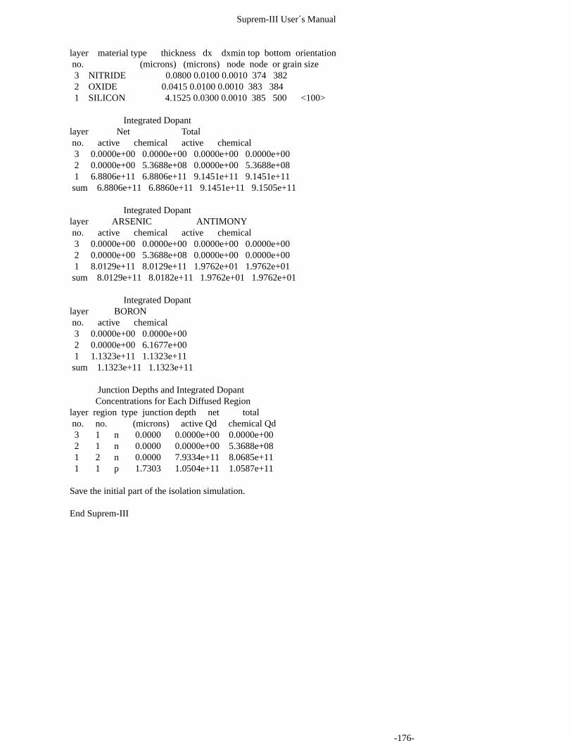
Suprem-III User´s Manual
layer material type thickness dx dxmin top bottom orientationno. (microns) (microns) node node or grain size3 NITRIDE 0.0800 0.0100 0.0010 374 3822 OXIDE 0.0415 0.0100 0.0010 383 3841 SILICON 4.1525 0.0300 0.0010 385 500 <100>
Integrated Dopantlayer Net Totalno. active chemical active chemical3 0.0000e+00 0.0000e+00 0.0000e+00 0.0000e+002 0.0000e+00 5.3688e+08 0.0000e+00 5.3688e+081 6.8806e+11 6.8806e+11 9.1451e+11 9.1451e+11sum 6.8806e+11 6.8860e+11 9.1451e+11 9.1505e+11
Integrated Dopantlayer ARSENIC ANTIMONYno. active chemical active chemical3 0.0000e+00 0.0000e+00 0.0000e+00 0.0000e+002 0.0000e+00 5.3688e+08 0.0000e+00 0.0000e+001 8.0129e+11 8.0129e+11 1.9762e+01 1.9762e+01sum 8.0129e+11 8.0182e+11 1.9762e+01 1.9762e+01
Integrated Dopantlayer BORONno. active chemical3 0.0000e+00 0.0000e+002 0.0000e+00 6.1677e+001 1.1323e+11 1.1323e+11sum 1.1323e+11 1.1323e+11
Junction Depths and Integrated DopantConcentrations for Each Diffused Region
layer region type junction depth net totalno. no. (microns) active Qd chemical Qd3 1 n 0.0000 0.0000e+00 0.0000e+002 1 n 0.0000 0.0000e+00 5.3688e+081 2 n 0.0000 7.9334e+11 8.0685e+111 1 p 1.7303 1.0504e+11 1.0587e+11
Save the initial part of the isolation simulation.
End Suprem-III
-176-

Suprem-III User´s Manual
Suprem-III simulation of the field oxide isolation region after drive-inof the buried layer.
-177-

Suprem-III User´s Manual
Suprem-III simulation of the field oxide isolation region after epigrowth and oxide/nitride deposition.
-178-

Suprem-III User´s Manual
************************************ Suprem-III ****** version 1B rev. 8628 ************************************
Tue Oct 27 16:38:59 1987
Commands input from file: s3ex2e.in
1... Title Suprem-III Example 2. Bipolar Poly doped emitter.2... $ Final isolation region formation.3... $ File s3ex2e.
4... Comment Start with the result of S3EX2D.5... Initialize Structure=s3e2ds Thickness=6
6... Comment Etch the nitride and oxide layers.7... Etch Nitride8... Etch Oxide
9... Comment Etch half the silicon epi layer.10... Etch Silicon Amount=.8
11... Comment Implant boron in the field region.12... Implant Boron Dose=2E13 Energy=100
13... Comment Grow the field oxide.14... Diffusion Temperature=800 Time=30 T.Rate=1015... Diffusion Temperature=1100 Time=15 DryO216... Diffusion Temperature=1100 Time=210 WetO217... Diffusion Temperature=1100 Time=15 DryO218... Diffusion Temperature=1100 Time=10 T.Rate=-3019... Print Layer
20... Comment Implant the boron base.21... Implant Boron Dose=1E14 Energy=80
22... Comment Deposit arsenic doped polysilicon for the emitter contact.23... Deposit Polysilicon, Thickness=.5 Temperature=620.... + Arsenic Concentration=1E20
24... Comment Remove the polysilicon.25... Etch Polysilicon
26... Comment Anneal to activate base and emitter regions.27... Diffusion Temperature=1000 Time=20 WetO2
28... Comment Plot the electrically active impurity distributions.29... Print Layer30... Plot Active Boron Xmax=5 Clear ˆAxis Linetype=231... Plot Active Arsenic Xmax=5 ˆClear ˆAxis Linetype=432... Plot Active Antimony Xmax=5 ˆClear ˆAxis Linetype=533... Plot Active Net Xmax=5 ˆClear Axis Linetype=1
34... Comment Save the final isolation region simulation.35... Savefile Structure File=s3e2es
-179-

Suprem-III User´s Manual
36... Stop
-180-

Suprem-III User´s Manual
Suprem-III Example 2. Bipolar Poly doped emitter.Final isolation region formation.File s3ex2e.Start with the result of S3EX2D.
Etch the nitride and oxide layers.
Etch half the silicon epi layer.
Implant boron in the field region.
Grow the field oxide.
layer material type thickness dx dxmin top bottom orientationno. (microns) (microns) node node or grain size2 OXIDE 1.2354 0.0100 0.0010 407 4241 SILICON 4.6564 0.0300 0.0010 425 500 <100>
Integrated Dopantlayer Net Totalno. active chemical active chemical2 0.0000e+00 -1.3720e+13 0.0000e+00 1.3992e+131 -4.8603e+12 -4.8603e+12 5.3040e+12 5.3040e+12sum -4.8603e+12 -1.8580e+13 5.3040e+12 1.9296e+13
Integrated Dopantlayer ARSENIC ANTIMONYno. active chemical active chemical2 0.0000e+00 1.3628e+11 0.0000e+00 3.3793e-011 2.2189e+11 2.2189e+11 1.9424e+01 1.9424e+01sum 2.2189e+11 3.5816e+11 1.9424e+01 1.9762e+01
Integrated Dopantlayer BORONno. active chemical2 0.0000e+00 1.3856e+131 5.0822e+12 5.0822e+12sum 5.0822e+12 1.8938e+13
Junction Depths and Integrated DopantConcentrations for Each Diffused Region
layer region type junction depth net totalno. no. (microns) active Qd chemical Qd2 1 p 0.0000 0.0000e+00 1.3992e+131 2 n 0.0000 5.9448e+09 5.1887e+101 1 p 0.0404 4.8305e+12 5.2176e+12
Implant the boron base.
Deposit arsenic doped polysilicon for the emitter contact.
Remove the polysilicon.
Anneal to activate base and emitter regions.
Plot the electrically active impurity distributions.
-181-
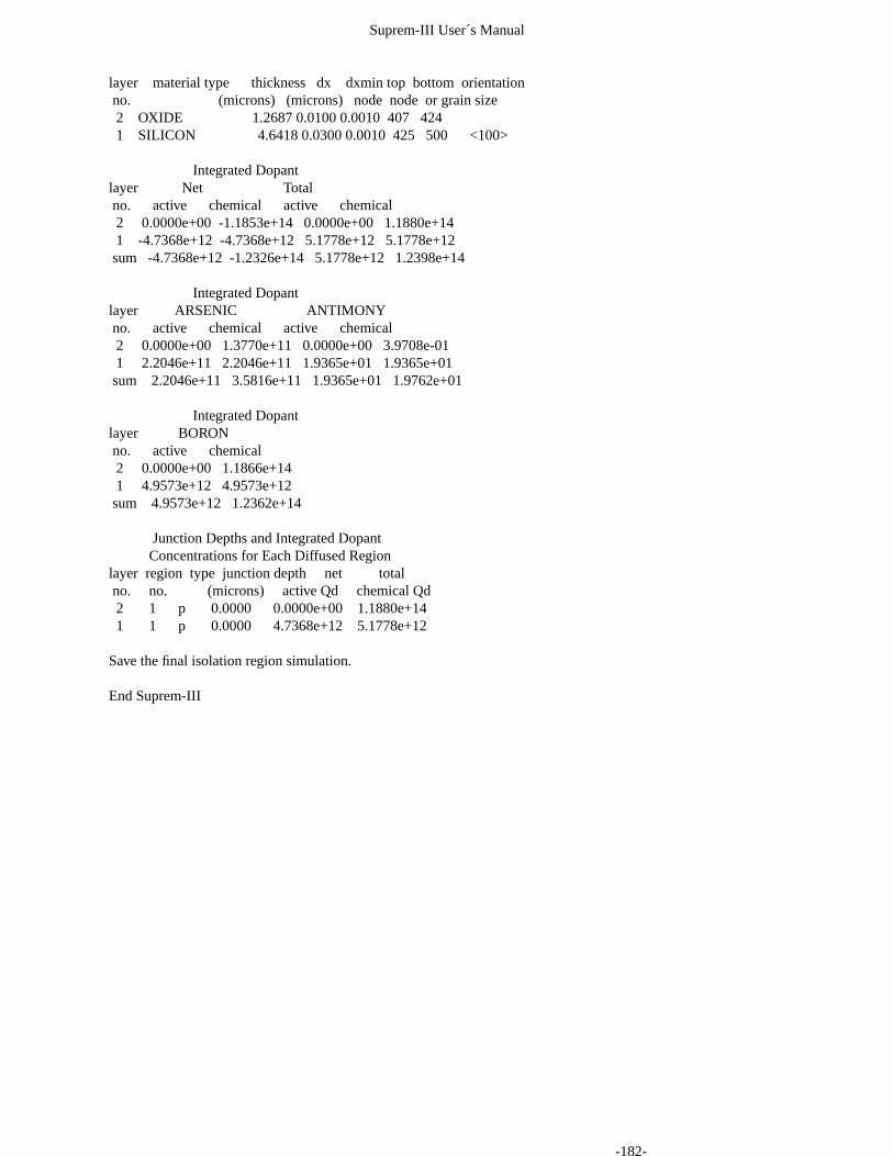
Suprem-III User´s Manual
layer material type thickness dx dxmin top bottom orientationno. (microns) (microns) node node or grain size2 OXIDE 1.2687 0.0100 0.0010 407 4241 SILICON 4.6418 0.0300 0.0010 425 500 <100>
Integrated Dopantlayer Net Totalno. active chemical active chemical2 0.0000e+00 -1.1853e+14 0.0000e+00 1.1880e+141 -4.7368e+12 -4.7368e+12 5.1778e+12 5.1778e+12sum -4.7368e+12 -1.2326e+14 5.1778e+12 1.2398e+14
Integrated Dopantlayer ARSENIC ANTIMONYno. active chemical active chemical2 0.0000e+00 1.3770e+11 0.0000e+00 3.9708e-011 2.2046e+11 2.2046e+11 1.9365e+01 1.9365e+01sum 2.2046e+11 3.5816e+11 1.9365e+01 1.9762e+01
Integrated Dopantlayer BORONno. active chemical2 0.0000e+00 1.1866e+141 4.9573e+12 4.9573e+12sum 4.9573e+12 1.2362e+14
Junction Depths and Integrated DopantConcentrations for Each Diffused Region
layer region type junction depth net totalno. no. (microns) active Qd chemical Qd2 1 p 0.0000 0.0000e+00 1.1880e+141 1 p 0.0000 4.7368e+12 5.1778e+12
Save the final isolation region simulation.
End Suprem-III
-182-

Suprem-III User´s Manual
Suprem-III simulation through the field oxide isolation region after allprocessing steps. Isolation has been achieved since the substrate is allp type, although barely. The base implant is also seen in the field ox-ide.
-183-

Suprem-III User´s Manual
51. Suggestions and Bug Reports----------------------------------------
In any program of the size of Suprem-III there is bound to be at least one bug (Do I hear some laughter?).And even if everything works as claimed, there will always be room for improvement. Therefore, I am listing bothan electronic and U.S. mail address for such things as bug reports, suggestions, complaints, and compliments (ifany).
Please send as much detail as possible about the problem and especially indicate which version of the pro-gram you are using and what system you are working on.
Electronic Mail U.S Mail
via INTERNET: [email protected] c/o Stephen E. Hansen
Applied Electronics Labsvia BITNET: Stanford UniversitySUP3BUGS%OASIS@STANFORD Stanford, California
94305via USENET (UUCP):{ucbvax,hplabs,decwrl,ihnp4}!{glacier,shasta}!oasis!sup3bugs
via CSNET:sup3bugs%[email protected]
If you can manage it I really prefer electronic mail as it makes response easier. In either case the responsetime will depend on a number of factors, primarily the severity of the problem.
Your feedback is crucial and appreciated!
Thanks,
Stephen E. Han
-184-

Suprem-III User´s Manual
1. Table Of Contents _________________________________________________________________________________________2. Introduction ______________________________________________________________________________________________3. The Simulation Structure ___________________________________________________________________________________4. Using SUPREM-III ________________________________________________________________________________________5. The SUPREM-III Grid Structure _____________________________________________________________________________6. SUPREM-III Output _______________________________________________________________________________________7. SUPREM-III Input Statements _______________________________________________________________________________8. Manual Format ___________________________________________________________________________________________9. Aluminum Statement ______________________________________________________________________________________10. Aluminum Statement ______________________________________________________________________________________11. Antimony Statement ______________________________________________________________________________________12. Arsenic Statement ________________________________________________________________________________________13. Bias Statement ___________________________________________________________________________________________14. Boron Statement __________________________________________________________________________________________15. Comment Statement _______________________________________________________________________________________16. Deposition Statement ______________________________________________________________________________________17. Diffusion Statement _______________________________________________________________________________________18. DryO2 Statement _________________________________________________________________________________________19. Electrical Statement _______________________________________________________________________________________20. End.Electrical Statement ___________________________________________________________________________________21. Epitaxy Statement ________________________________________________________________________________________22. Etch Statement ___________________________________________________________________________________________23. Grid Statement ___________________________________________________________________________________________24. Implant Statement ________________________________________________________________________________________25. Impurity Statement ________________________________________________________________________________________26. Initialize Statement _______________________________________________________________________________________27. Loadfile Statement ________________________________________________________________________________________28. Lpplot Statement _________________________________________________________________________________________29. Material Statement ________________________________________________________________________________________30. Nitride Statement _________________________________________________________________________________________31. Nitrogen Statement _______________________________________________________________________________________32. Oxide Statement __________________________________________________________________________________________33. Phosphorus Statement _____________________________________________________________________________________34. Plot Statement ___________________________________________________________________________________________35. Polysilicon Statement _____________________________________________________________________________________36. Print Statement ___________________________________________________________________________________________37. Profile Statement _________________________________________________________________________________________38. Resistivity Statement ______________________________________________________________________________________39. Savefile Statement ________________________________________________________________________________________40. Segregation Statement _____________________________________________________________________________________41. Silicon Statement _________________________________________________________________________________________42. Solubility Statement _______________________________________________________________________________________43. Stop Statement ___________________________________________________________________________________________44. Title Statement ___________________________________________________________________________________________45. Vol.Ratio Statement _______________________________________________________________________________________46. V.Threshold Statement _____________________________________________________________________________________47. WetO2 Statement _________________________________________________________________________________________48. Statement Summary _______________________________________________________________________________________49. Example 1: NMOS Silicon Gate. _____________________________________________________________________________50. Example 2: Bipolar Polysilicon Doped Emitter. _________________________________________________________________51. Suggestions and Bug Reports _______________________________________________________________________________
-185-