Supporting Information for · 2017-02-03 · Fig. SI1. Band structures of S1, S2, and Gulay...
7
Supporting Information for The “Electron Crystal” Behavior in Copper Chalcogenides Cu 2 X (X=Se, S) Yongxing Sun 1,2,3 , Lili Xi 1,3 , Jiong Yang 1* , Lihua Wu 1 , Xun Shi 3 , Lidong Chen 3 , Jeffrey Snyder 4 , Jihui Yang 5 , and Wenqing Zhang 1,2* 1) Materials Genome Institute, Shanghai University, Shanghai 200444, China 2) School of Materials Science and Engineering, Shanghai University, Shanghai 200444, China 3) State Key Laboratory of High Performance Ceramics and Superfine Microstructure, Shanghai Institute of Ceramics, Chinese Academy of Sciences, Shanghai 200050, China 4) Department of Materials Science and Engineering, Northwestern University, Evanston, Illinois 60208, USA 5) Material Science and Engineering Department, University of Washington, Seattle, WA 98195, USA This supporting information includes: Fig. SI1. Band structures of S1, S2, and Gulay structures. Fig. SI2. The pCOHP analysis for the Cu-Se bond in Cu 2 Se with the antifluorite structure. Fig. SI3. The band structure of S3 Cu 2 Se with some Se vacancy. Fig. SI4. Electronic band structures of Cu 1.92 Se in the low temperature S3 structure, with the Cu vacancy locating at different Cu sites. Fig. SI5. Electronic band structures of Cu 2 Se, Cu 1.96 Se, Cu 1.93 Se, and Cu 2 Se with all Cu ions disordered. Fig. SI6. Theoretical absolute electrical conductivities as a function of hole concentrations at 300K and 800K. Fig. SI7. Wave functions at the valence band maxima for both LT and HT Cu 2 Se. Table SI1. Structural parameters and atomic coordinates for S1, S2, S3 and Gulay structures. Electronic Supplementary Material (ESI) for Journal of Materials Chemistry A. This journal is © The Royal Society of Chemistry 2017
Transcript of Supporting Information for · 2017-02-03 · Fig. SI1. Band structures of S1, S2, and Gulay...

Supporting Information for
The “Electron Crystal” Behavior in Copper Chalcogenides Cu2X (X=Se, S)
Yongxing Sun1,2,3, Lili Xi1,3, Jiong Yang1*, Lihua Wu1, Xun Shi3, Lidong Chen3, Jeffrey Snyder4, Jihui
Yang5, and Wenqing Zhang1,2*
1)Materials Genome Institute, Shanghai University, Shanghai 200444, China2) School of Materials Science and Engineering, Shanghai University, Shanghai 200444, China
3) State Key Laboratory of High Performance Ceramics and Superfine Microstructure, Shanghai Institute of
Ceramics, Chinese Academy of Sciences, Shanghai 200050, China4)Department of Materials Science and Engineering, Northwestern University, Evanston, Illinois 60208,
USA5) Material Science and Engineering Department, University of Washington, Seattle, WA 98195, USA
This supporting information includes:
Fig. SI1. Band structures of S1, S2, and Gulay structures.
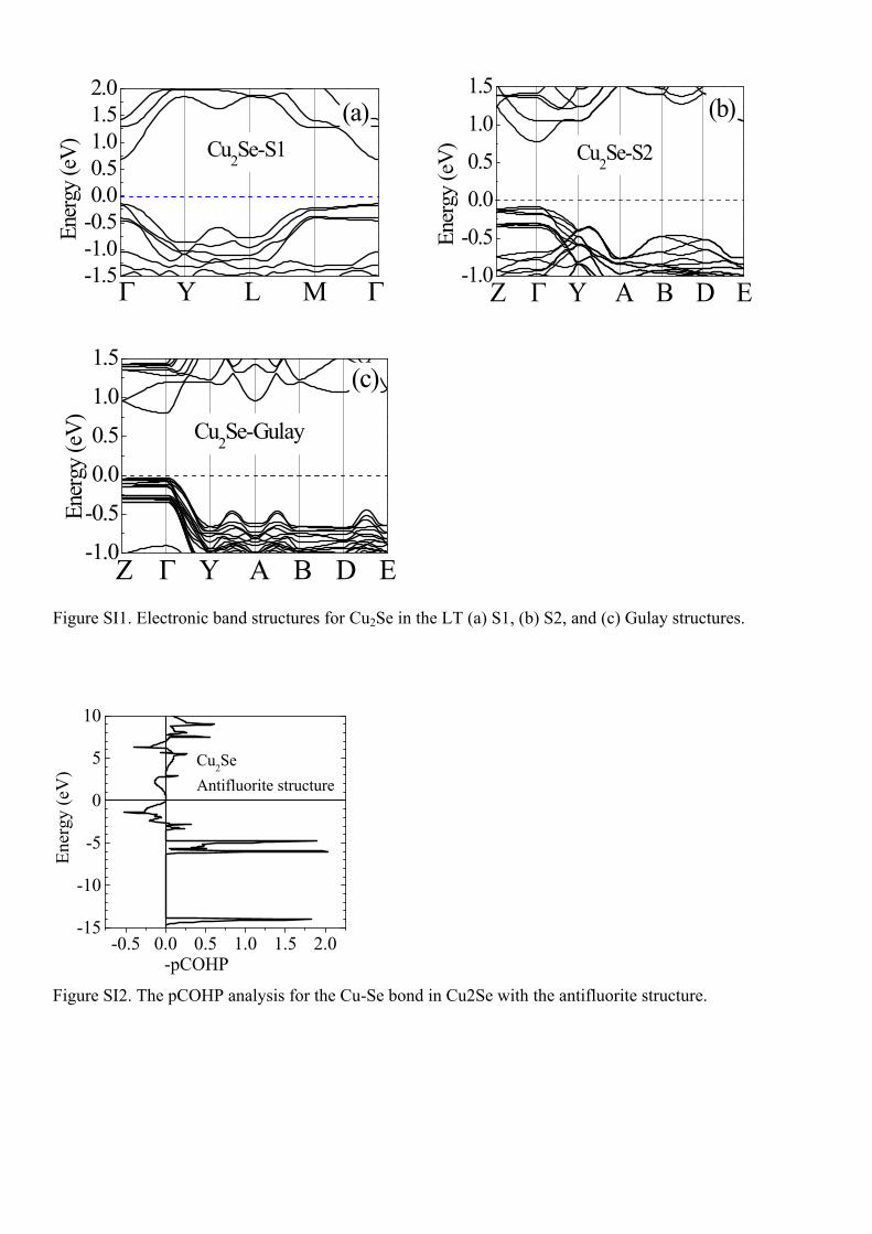
Fig. SI2. The pCOHP analysis for the Cu-Se bond in Cu2Se with the antifluorite structure.
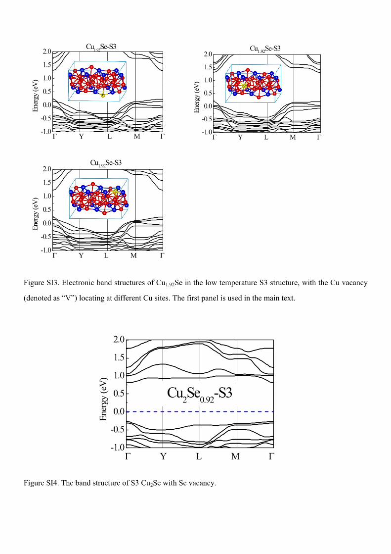
Fig. SI3. The band structure of S3 Cu2Se with some Se vacancy.
Fig. SI4. Electronic band structures of Cu1.92Se in the low temperature S3 structure, with the Cu
vacancy locating at different Cu sites.
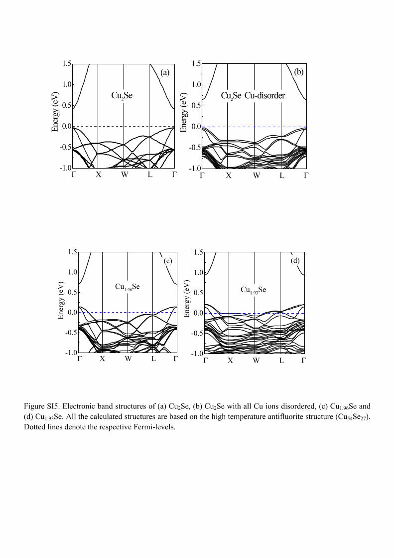
Fig. SI5. Electronic band structures of Cu2Se, Cu1.96Se, Cu1.93Se, and Cu2Se with all Cu ions disordered.
Fig. SI6. Theoretical absolute electrical conductivities as a function of hole concentrations at 300K and
800K.
Fig. SI7. Wave functions at the valence band maxima for both LT and HT Cu2Se.
Table SI1. Structural parameters and atomic coordinates for S1, S2, S3 and Gulay structures.
Electronic Supplementary Material (ESI) for Journal of Materials Chemistry A.This journal is © The Royal Society of Chemistry 2017
-1.5-1.0-0.50.00.51.01.52.0
Ener
gy (e
V) Cu2Se-S1(a)
Y L M -1.0
-0.5
0.0
0.5
1.0
1.5
Y A B D
Ener
gy (e
V) Cu2Se-S2
(b)
-1.0
-0.5
0.0
0.5
1.0
1.5
Y A B D
Cu2Se-Gulay
(c)
Ener
gy (e
V)
Figure SI1. Electronic band structures for Cu2Se in the LT (a) S1, (b) S2, and (c) Gulay structures.
-0.5 0.0 0.5 1.0 1.5 2.0-15
-10
-5
0
5
10
Ener
gy (e
V)
-pCOHP
Cu2SeAntifluorite structure
Figure SI2. The pCOHP analysis for the Cu-Se bond in Cu2Se with the antifluorite structure.
-1.0
-0.5
0.0
0.5
1.0
1.5
2.0 Cu1.92Se-S3En
ergy
(eV)
Y L M -1.0
-0.5
0.0
0.5
1.0
1.5
2.0Cu1.92Se-S3
Ener
gy (e
V)
Y L M
-1.0
-0.5
0.0
0.5
1.0
1.5
2.0Cu1.92Se-S3
Ener
gy (e
V)
Y L M
Figure SI3. Electronic band structures of Cu1.92Se in the low temperature S3 structure, with the Cu vacancy
(denoted as “V”) locating at different Cu sites. The first panel is used in the main text.
-1.0
-0.5
0.0
0.5
1.0
1.5
2.0
Cu2Se0.92-S3
Ener
gy (e
V)
Y L M
Figure SI4. The band structure of S3 Cu2Se with Se vacancy.
-1.0
-0.5
0.0
0.5
1.0
1.5
-1.0
-0.5
0.0
0.5
1.0
1.5(b)(a)
Ener
gy (e
V)Cu2Se
Ener
gy (e
V)
X W L X W L
Cu2Se Cu-disorder
-1.0
-0.5
0.0
0.5
1.0
1.5
-1.0
-0.5
0.0
0.5
1.0
1.5(c) (d)
Ener
gy (e
V)
Ener
gy (e
V)
Cu1.93Se
X W L X W L
Cu1.96Se
Figure SI5. Electronic band structures of (a) Cu2Se, (b) Cu2Se with all Cu ions disordered, (c) Cu1.96Se and (d) Cu1.93Se. All the calculated structures are based on the high temperature antifluorite structure (Cu54Se27). Dotted lines denote the respective Fermi-levels.
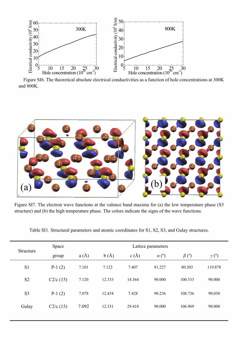
5 10 15 20 25 300102030405060
Hole concentration (1020 cm-3)
300KEl
ectri
cal c
ondu
ctivi
ty (1
04 S/m
)
5 10 15 20 25 300
10
20
30
40
50
Hole concentration (1020 cm-3)
800K
Elec
trica
l con
ducti
vity
(104 S
/m)
Figure SI6. The theoretical absolute electrical conductivities as a function of hole concentrations at 300K and 800K.
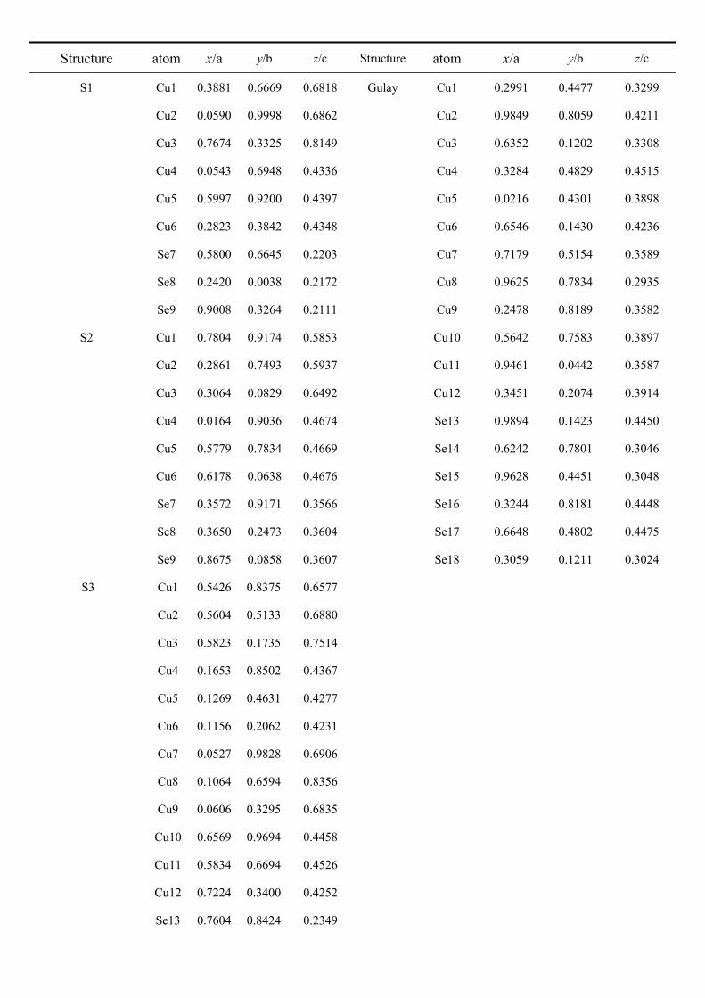
(a) (b)
Figure SI7. The electron wave functions at the valence band maxima for (a) the low temperature phase (S3 structure) and (b) the high temperature phase. The colors indicate the signs of the wave functions.
Table SI1. Structural parameters and atomic coordinates for S1, S2, S3, and Gulay structures.
Lattice parametersStructure
Space
group a (Å) b (Å) c (Å) α (º) β (º) γ (º)
S1 P-1 (2) 7.101 7.122 7.407 81.227 80.503 119.878
S2 C2/c (15) 7.120 12.333 14.364 90.000 100.333 90.000
S3 P-1 (2) 7.078 12.434 7.428 90.236 108.736 90.038
Gulay C2/c (15) 7.092 12.331 29.418 90.000 106.969 90.000
Structure atom x/a y/b z/c Structure atom x/a y/b z/c
S1 Cu1 0.3881 0.6669 0.6818 Gulay Cu1 0.2991 0.4477 0.3299
Cu2 0.0590 0.9998 0.6862 Cu2 0.9849 0.8059 0.4211
Cu3 0.7674 0.3325 0.8149 Cu3 0.6352 0.1202 0.3308
Cu4 0.0543 0.6948 0.4336 Cu4 0.3284 0.4829 0.4515
Cu5 0.5997 0.9200 0.4397 Cu5 0.0216 0.4301 0.3898
Cu6 0.2823 0.3842 0.4348 Cu6 0.6546 0.1430 0.4236
Se7 0.5800 0.6645 0.2203 Cu7 0.7179 0.5154 0.3589
Se8 0.2420 0.0038 0.2172 Cu8 0.9625 0.7834 0.2935
Se9 0.9008 0.3264 0.2111 Cu9 0.2478 0.8189 0.3582
S2 Cu1 0.7804 0.9174 0.5853 Cu10 0.5642 0.7583 0.3897
Cu2 0.2861 0.7493 0.5937 Cu11 0.9461 0.0442 0.3587
Cu3 0.3064 0.0829 0.6492 Cu12 0.3451 0.2074 0.3914
Cu4 0.0164 0.9036 0.4674 Se13 0.9894 0.1423 0.4450
Cu5 0.5779 0.7834 0.4669 Se14 0.6242 0.7801 0.3046
Cu6 0.6178 0.0638 0.4676 Se15 0.9628 0.4451 0.3048
Se7 0.3572 0.9171 0.3566 Se16 0.3244 0.8181 0.4448
Se8 0.3650 0.2473 0.3604 Se17 0.6648 0.4802 0.4475
Se9 0.8675 0.0858 0.3607 Se18 0.3059 0.1211 0.3024
S3 Cu1 0.5426 0.8375 0.6577
Cu2 0.5604 0.5133 0.6880
Cu3 0.5823 0.1735 0.7514
Cu4 0.1653 0.8502 0.4367
Cu5 0.1269 0.4631 0.4277
Cu6 0.1156 0.2062 0.4231
Cu7 0.0527 0.9828 0.6906
Cu8 0.1064 0.6594 0.8356
Cu9 0.0606 0.3295 0.6835
Cu10 0.6569 0.9694 0.4458
Cu11 0.5834 0.6694 0.4526
Cu12 0.7224 0.3400 0.4252
Se13 0.7604 0.8424 0.2349

Se14 0.7425 0.5066 0.2227
Se15 0.7339 0.1729 0.2094
Se16 0.2486 0.9968 0.2164
Se17 0.2438 0.6554 0.2172
Se18 0.2444 0.3240 0.2049