Supply Voltage Dependence of Heavy Ion Induced SEEs on ...
120
Supply Voltage Dependence of Heavy Ion Induced SEEs on 65nm CMOS Bulk SRAMs A Thesis Submitted to the College of Graduate Studies and Research In Partial Fulfillment of the Requirements For the Degree of Master of Science In the Department of Electrical and Computer Engineering University of Saskatchewan Saskatoon By QIONG WU Copyright Qiong Wu, June, 2015. All rights reserved.
Transcript of Supply Voltage Dependence of Heavy Ion Induced SEEs on ...
Supply Voltage Dependence of Heavy Ion Induced SEEs
on 65nm CMOS Bulk SRAMs
A Thesis Submitted to the College of
Graduate Studies and Research
In Partial Fulfillment of the Requirements
For the Degree of Master of Science
In the Department of Electrical and Computer Engineering
University of Saskatchewan
Saskatoon
By
QIONG WU
Copyright Qiong Wu, June, 2015. All rights reserved.

i
PERMISSION TO USE
In presenting this thesis in partial fulfilment of the requirements for a Postgraduate
degree from the University of Saskatchewan, I agree that the Libraries of this University may
make it freely available for inspection. I further agree that permission for copying of this
thesis in any manner, in whole or in part, for scholarly purposes may be granted by the
professor or professors who supervised my thesis work or, in their absence, by the Head of
the Department or the Dean of the College in which my thesis work was done. It is
understood that any copying or publication or use of this thesis or parts thereof for financial
gain shall not be allowed without my written permission. It is also understood that due
recognition shall be given to me and to the University of Saskatchewan in any scholarly use
which may be made of any material in my thesis.
Requests for permission to copy or to make other use of material in this thesis in
whole or part should be addressed to:
Head of the Department of Electrical and Computer Engineering
57 Campus Drive
University of Saskatchewan
Saskatoon, Saskatchewan
Canada
S7N 5A9
ii
ACKNOWLEDGEMENT
None of my accomplishments would be possible without the support and assistance of
numerous individuals. First of all, I would like to thank Dr. Li Chen, my supervisor during
my postgraduate studies at University of Saskatchewan. Dr. Chen has been incredibly helpful
and truly an inspiration on both professional and personal levels. He was always there to lend
advice when I asked and to give motivation when I needed it. Additionally, financial
assistance provided by the Dr. Li Chen and University of Saskatchewan through research
funding and Graduate Scholarship is thankfully acknowledged.
Thank you to my fellow graduate students, with whom I have spent so much time. I
also want to express my sincere gratitude to Rui Liu and Yuanqing Li for all of their help
with chip fabrication and data analysis. Thank you to everyone else past and present in room
2B60 and 3C80 of Engineering Building. Also, I would like to acknowledge the staff and
faculty of the Electrical and Computer Engineering Department for their support. They all
have helped me in different ways over the course of this work.
Lastly and with the most gravity, I would like to express my deepest gratitude to my
husband. I am grateful to my parents, for their unselfish love and constant support. They have
encouraged my education, instilled honesty, and nurtured a predilection to science.
iii
ABSTRACT
The power consumption of Static Random Access Memory (SRAM) has become an
important issue for modern integrated circuit design, considering the fact that they occupy
large area and consume significant portion of power consumption in modern nanometer chips.
SRAM operating in low power supply voltages has become an effective approach in reducing
power consumption. Therefore, it is essential to experimentally characterize the single event
effects (SEE) of hardened and unhardened SRAM cells to determine their appropriate
applications, especially when a low supply voltage is preferred. In this thesis, a SRAM test
chip was designed and fabricated with four cell arrays sharing the same peripheral circuits,
including two types of unhardened cells (standard 6T and sub-threshold 10T) and two types
of hardened cells (Quatro and DICE). The systems for functional and radiation tests were
built up with power supply voltages that ranged from near threshold 0.4 V to normal supply 1
V. The test chip was irradiated with alpha particles and heavy ions with various linear energy
transfers (LETs) at different core supply voltages, ranging from 1 V to 0.4 V. Experimental
results of the alpha test and heavy ion test were consistent with the results of the simulation.
The cross sections of 6T and 10T cells present much more significant sensitivities than
Quatro and DICE cells for all tested supply voltages and LET. The 10T cell demonstrates a
more optimal radiation performance than the 6T cell when LET is small (0.44 MeV·cm2/mg),
yet no significant advantage is evident when LET is larger than this. In regards to the Quatro
and DICE cells, one does not consistently show superior performance over the other in terms
of soft error rates (SERs). Multi-bit upsets (MBUs) occupy a larger portion of total SEUs in
DICE cell when relatively larger LET and smaller supply voltage are applied. It explains the
iv
loss in radiation tolerance competition with Quatro cell when LET is bigger than 9.1
MeV·cm2/mg and supply voltage is smaller than 0.6 V. In addition, the analysis of test results
also demonstrated that the error amount distributions follow a Poisson distribution very well
for each type of cell array.
v
TABLE OF CONTENTS
PERMISSION TO USE .............................................................................................................. i
ACKNOWLEDGEMENT ......................................................................................................... ii
ABSTRACT ............................................................................................................................. iii
TABLE OF CONTENTS ........................................................................................................... v
LIST OF FIGURES .................................................................................................................. ix
LIST OF TABLES ................................................................................................................. xiii
LIST OF ABBREVIATIONS ................................................................................................. xiv
CHAPTER 1 .............................................................................................................................. 1
BACKGROUND AND MOTIVATION ............................................................................. 1
1.1 Background and motivation .............................................................................................. 1
1.2 Objectives ......................................................................................................................... 3
1.3 Thesis Outline ................................................................................................................... 4
CHAPTER 2 .............................................................................................................................. 5
INTRODUCTION .............................................................................................................. 5
2.1 Conventional 6T SRAM cell ............................................................................................ 5
2.1.1 Write Operation ....................................................................................................... 6
2.1.2 Read Operation ....................................................................................................... 8
2.2 Challenges for Low Power Operation ............................................................................. 10
2.2.1 Static Noise Margin .............................................................................................. 10
Previous designs to improve the RSNM .................................................................... 12
2.2.2 Bitline leakage ...................................................................................................... 15
vi
Previous design to reduce bitline leakage .................................................................. 17
2.2.3 Low Writability ..................................................................................................... 20
2.3 Fault-tolerant Design ...................................................................................................... 21
2.3.1 Single Event Upset ................................................................................................ 21
2.3.2 SEUs in SRAM ..................................................................................................... 23
2.3.3 Radiation Tolerant SRAM Design ........................................................................ 25
2.3.3.1 Dual Interlocked Storage Cell ..................................................................... 25
2.3.3.2 Quatro cell ................................................................................................... 27
CHAPTER 3 ............................................................................................................................ 36
SRAM DESIGN................................................................................................................ 36
3.1 Memory Design Overview ................................................................................................. 36
3.2 Memory Cells and Peripheral Circuits Design .................................................................. 38
3.1.1 Memory cell design.................................................................................................. 39
3.1.1.1 Conventional 6T cell ...................................................................................... 39
3.1.1.2 10T cell .......................................................................................................... 40
3.1.1.3 Modified DICE cell........................................................................................ 41
3.1.1.4 Quatro Cell ..................................................................................................... 43
3.1.2 Address Decoders ................................................................................................. 43
3.1.3 Multiplexer ............................................................................................................ 45
3.1.4 Bitline Conditioning.............................................................................................. 46
3.1.5 Sense Amplifier ..................................................................................................... 48
3.1.6 Write Circuit ......................................................................................................... 50
vii
3.1.7 Level Shifter.......................................................................................................... 51
3.2 Write Operation ............................................................................................................... 53
3.3 Read Operation ............................................................................................................... 55
3.4 Layout of the SRAM ....................................................................................................... 56
CHAPTER 4 ............................................................................................................................ 60
SIMULATION RESULTs ................................................................................................. 60
4.1 Memory cell simulation .................................................................................................. 60
4.1.1 Signal Noise Margin ............................................................................................. 60
4.1.2 Read and write simulations ................................................................................... 62
4.1.2 Critical Charge ...................................................................................................... 64
4.2 Simulation of Sense Amplifier ........................................................................................ 67
4.3 Simulation of Level Shifter ............................................................................................. 69
4.4 Simulation of Whole SRAM ........................................................................................... 71
CHAPTER 5 ............................................................................................................................ 75
TEST RESULT ................................................................................................................. 75
5.1 Test system setup ....................................................................................................... 75
5.2 Functional Test ................................................................................................................ 77
5.3 Radiation Test ................................................................................................................. 81
5.3.1 Alpha Radiation Test ............................................................................................. 82
5.3.2 Heavy Ion Radiation Test ...................................................................................... 84
5.3.3 Cross Section Analysis .......................................................................................... 86
5.3.4 Bit-Cell Upsets Distributions Analysis ................................................................. 93
viii
CHAPTER 6 ............................................................................................................................ 96
CONCLUSION AND FUTURE WORK .......................................................................... 96
6.1 Conclusions ..................................................................................................................... 96
6.2 Future work ..................................................................................................................... 97
REFERENCES ........................................................................................................................ 99
ix
LIST OF FIGURES
Figure 2.1 Conventional 6T SRAM cell ................................................................................. 5
Figure 2.2 Simplified model of 6T cell during write (Q= ‘1’) ................................................ 7
Figure 2.3 Write operation for 6T SRAM cell ........................................................................ 7
Figure 2.4 Simplified model of 6T cell during write (Q= ‘1’) ................................................ 9
Figure 2.5 Read operation for 6T SRAM cell ......................................................................... 9
Figure 2.6 Cross-coupled inverters with noise source for HSNM simulation [24] .............. 10
Figure 2.7 Cross-coupled inverters with noise source for RSNM simulation [24] .............. 10
Figure 2.8 Butterfly diagram indicating HSNM ................................................................... 11
Figure 2.9 Butterfly diagram indicating RSNM ................................................................... 11
Figure 2.10 Schematic of 8T SRAM cell [25] ...................................................................... 12
Figure 2.11 Schematic of Chang’s 10T SRAM cell [13] ...................................................... 14
Figure 2.12 Read and write operation of Chang’s 10T cell [13] .......................................... 14
Figure 2.13 Worst case for bitline leakage [10] .................................................................... 15
Figure 2.14 Large data dependency induced by bitline leakage [11] ................................... 16
Figure 2.15 Schematic of Kim’s 10T cell [11] ...................................................................... 17
Figure 2.16 Improved small data dependency by bitline leakage [11] ................................. 18
Figure 2.17 Leakage with read buffer feet structure ............................................................. 19
Figure 2.18 Boost circuit to drive read buffer [10] ............................................................... 20
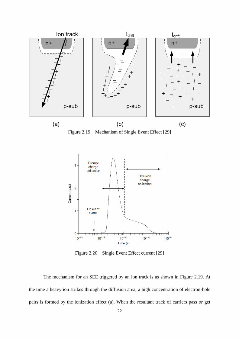
Figure 2.19 Mechanism of Single Event Effect [29] ............................................................ 22
Figure 2.20 Single Event Effect current [29] ........................................................................ 22
Figure 2.21 SEU in SRAM cell ............................................................................................ 24
x
Figure 2.22 Schematic of DICE cell [21] ............................................................................. 25
Figure 2.23 Simulation result of SEU effect on DICE cell ................................................... 26
Figure 2.24 Schematic of Quatro cell [22]............................................................................ 27
Figure 2.25 Simplified model for write operation ................................................................ 28
Figure 2.26 Simulation waveforms of the storage nodes, wordline, and bitlines in a write
cycle ......................................................................................................................................... 29
Figure 2.27 Simplified model for a write operation ............................................................. 30
Figure 2.28 Simulation waveforms of the storage nodes, wordline, and bitlines in a write
cycle ......................................................................................................................................... 31
Figure 2.29 Recovery from injected current mimicking ‘1’ to ‘0’ at node A ....................... 32
Figure 2.30 Flipping of cell by injecting current mimicking ‘0’ to ‘1’ at node A ................. 33
Figure 2.31 Recovery from injected current mimicking ‘0’ to ‘1’ at node C ....................... 34
Figure 2.32 Flipping of cell by injecting current mimicking ‘1’ to ‘0’ at node C ................. 35
Figure 3.1 The block diagram for one page of the SRAM test chip ..................................... 37
Figure 3.3 Schematic of 10T cell .......................................................................................... 40
Figure 3.4 Schematic of low power operational DICE cell .................................................. 41
Figure 3.5 Schematic of an Quatro cell ................................................................................ 43
Figure 3.6 Pseudo read problem of hold cells....................................................................... 45
Figure 3.7 Global wordline and Local wordline [24] ........................................................... 45
Figure 3.8 Schematic of four to one multiplexer .................................................................. 46
Figure 3.9 Bitline conditioning circuit .................................................................................. 46
Figure 3.10 Controlled bitline conditioning circuit .............................................................. 47
xi
Figure 3.11 Timing sequence of Φ during read, write and hold operations .......................... 48
Figure 3.12 Schematic of latch based sense amplifier [40] .................................................. 49
Figure 3.13 Schematic of the write circuit ............................................................................ 51
Figure 3.14 Schematic of level-up shifter [41] ..................................................................... 52
Figure 3.15 SRAM writing diagram ..................................................................................... 53
Figure 3.16 Write timing sequence with VDD=1 V ............................................................. 54
Figure 3.17 SRAM reading diagram ..................................................................................... 55
Figure 3.18 Read timing sequence with VDD=1 V .............................................................. 56
Figure 3.19 Layout of one quadrant of the SRAM design .................................................... 57
Figure 3.20 Whole chip layout view ..................................................................................... 58
Figure 4.1 Read butterfly curves of the four SRAM cells .................................................... 61
Figure 4.2 Hold and read SNM of four cells from 0.3 V to 1 V ........................................... 62
Figure 4.3 Simulation results of BL, BLB and RWL during read cycle with VDD=1 V and
0.3 V ......................................................................................................................................... 63
Figure 4.4 Simulation results of storage nodes and RWL during read cycle with VDD=1 V
and 0.3 V .................................................................................................................................. 63
Figure 4.6 Monte Carlo simulation of sense amplifier with VDD=1 V ............................... 68
Figure 4.7 Monte Carlo simulation of sense amplifier with VDD=0.3 V ............................ 68
Figure 4.8 Level down shifter with output voltage 0.3 V and 0.7 V .................................... 70
Figure 4.9 Level up shifter with input voltage 0.3 V and 0.7 V ........................................... 71
Figure 4.10 Whole 6T SRAM with VDD=1 V ..................................................................... 72
Figure 4.11 Whole 6T SRAM with VDD=0.7 V .................................................................. 73
xii
Figure 4.10 Whole 6T SRAM with VDD=0.3 V .................................................................. 74
Figure 5.1 Photo of PCB with the SRAM chip soldered ...................................................... 75
Figure 5.2 SRAM testing system setup................................................................................. 76
Figure 5.3 SBU and MBU definition .................................................................................... 82
Figure 5.4 Heavy ion test environment setup ....................................................................... 85
Figure 5.5 Heavy ion test system .......................................................................................... 86
Figure 5.6 Cross section of the four SRAM cell arrays. ....................................................... 90
Figure 5.8 Bit-cell upsets distributions of SRAMs ............................................................... 94
xiii
LIST OF TABLES
Table 3.1 Characteristics of SRAM Cells ............................................................................. 39
Table 3.2 IO list for the SRAM chip ..................................................................................... 59
Table 4.1 Critical charge of four cells ................................................................................... 65
Table 5.1 Read error rates of the four cells from 0.3 V to 0.7 V........................................... 79
Table 5.2 Alpha particle radiation test result ........................................................................ 83
Table 5.3 Heavy Ions Parameters .......................................................................................... 85
Table 5.4 SBU and MBU Cross Sections of the Four SRAM Cell Arrays ........................... 93
xiv
LIST OF ABBREVIATIONS
CIAE China Institute of Atomic Energy
CQFP80 Ceramic Quad Flat Package
CR Cell Ratio
DICE Drain-Induced Barrier Lowering
DIBL Dual Interlocked Storage Cell
DIMM Dual In-line Memory Module
FPGA Field-Programmable Gate Array
HSNM Hold Signal Noise Margin
LET Linear Energy Transfer
MBU Multi-bit Upset
MNU Multi-node Upset
MUX Multiplexer
PCB Printed Circuit Board
PR Pull-up Ratio
RHBD Radiation Hardened by Design
RSCE Reverse Short Channel Effect
SA Sense Amplifier
SBU Single-bit Upset
SEE Single Event Effect
SER Soft Error Rate
SEU Single Event Upset
xv
SNM Signal Noise Margin
SRAM Static Random Access Memory
SSSC Saskatchewan Structural Sciences Centre
WSNM Write Signal Noise Margin
VTC Voltage Transfer Characteristic
1
CHAPTER 1
BACKGROUND AND MOTIVATION
1.1 Background and motivation
SRAM (Static Random Access Memory) occupies a large area of most modern
nanometer chips and consumes a large portion of power consumption [1]. With advanced
processes scaling down, power consumption has already become an important factor for
large-scale SRAMs design. SRAM operating in lower power supply voltages has become an
effective approach to reduce power consumptions. However, radiation immunity for memory
is also critical, considering the fact that the error caused by Single Event Upset (SEU) can be
“remembered” by the SRAM, ultimately resulting in a vital functionality fault. In addition,
lowering the supply voltage may also lead to the reduction of nodal critical charge, thus
imposing acute soft error threats due to single events on the reliable operations of SRAMs
[10]. Therefore, the estimations of SRAM Soft Error Rates (SER) versus voltage
relationships are critical in determining their appropriate applications.
In order to study the supply power dependence of radiation effects on SRAM,
especially in sub-threshold region, two factors must be studied: low power operational and
SEU tolerance.
With the increasing applications in space, biomedical, mobile and other battery based
devices, reducing the power dissipation has become an important objective in chip design.
The total power consumption in the chip can be divided to two portions: dynamic dissipation
and static dissipation, as shown in the equation below [2].
2
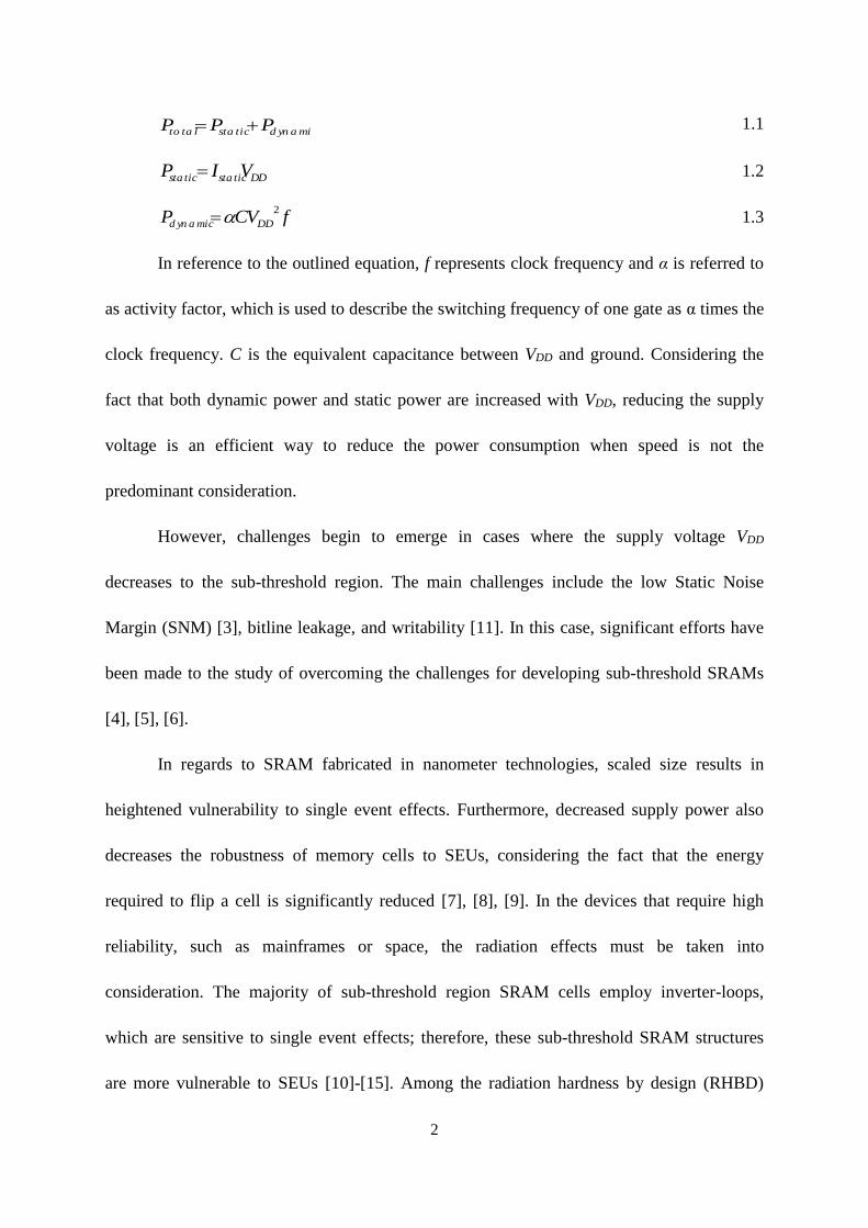
d yn a micsta ticto ta l PPP 1.1
DDsta ticsta tic VIP 1.2
fCVP DDd yn a mic
2 1.3
In reference to the outlined equation, f represents clock frequency and α is referred to
as activity factor, which is used to describe the switching frequency of one gate as α times the
clock frequency. C is the equivalent capacitance between VDD and ground. Considering the
fact that both dynamic power and static power are increased with VDD, reducing the supply
voltage is an efficient way to reduce the power consumption when speed is not the
predominant consideration.
However, challenges begin to emerge in cases where the supply voltage VDD
decreases to the sub-threshold region. The main challenges include the low Static Noise
Margin (SNM) [3], bitline leakage, and writability [11]. In this case, significant efforts have
been made to the study of overcoming the challenges for developing sub-threshold SRAMs
[4], [5], [6].
In regards to SRAM fabricated in nanometer technologies, scaled size results in
heightened vulnerability to single event effects. Furthermore, decreased supply power also
decreases the robustness of memory cells to SEUs, considering the fact that the energy
required to flip a cell is significantly reduced [7], [8], [9]. In the devices that require high
reliability, such as mainframes or space, the radiation effects must be taken into
consideration. The majority of sub-threshold region SRAM cells employ inverter-loops,
which are sensitive to single event effects; therefore, these sub-threshold SRAM structures
are more vulnerable to SEUs [10]-[15]. Among the radiation hardness by design (RHBD)

3
cells, the dual-interlocked storage cell (DICE) may be considered the most well-known and
widely used of these cells [16]. In 2009, another RHBD SRAM cell named Quatro was
proposed [17], which is a cell that uses fewer transistors as compared to DICE.
Correspondingly, radiation experiments (neutron, alpha, and heavy ions) demonstrated a
higher radiation tolerance than DICE in cases where both of the cells were used to construct
flip-flops in a 40nm technology [18].
In previous literature, the supply voltage dependences of alpha and neutron radiation
effects in unhardened SRAM cells have been studied in [19]-[21]. For a SRAM fabricated
with 90nm CMOS process, when supply voltage decreases by every 10%, the measured SER
induced by neutron increases by 18% [19]. It is also reported that the multi-bit upsets (MBU)
rate of a 65 nm 10T SRAM caused by alpha and neutron sources increase as the power
supply voltage decreases to sub-threshold [20] [21]. However, as far as the author knows,
supply power dependences on unhardened and hardened SRAMs when irradiated with heavy
ions have not been reported yet. The advantage of using heavy ions is that it is able to provide
a wider range of linear energy transfers (LETs) than alpha particles, as well as facilitating a
more accurate mechanism of the interactions with silicon [22]. Therefore, heavy ion
experiments on SRAMs can directly reveal the LET impact on the SER/voltage relationship.
1.2 Objectives
The objectives of this research are as follows:
1. The comprehensive study of supply power dependences of the single-event effects
(SEEs) of four different SRAM cells. Design and fabricate a SRAM with different
cells, some are normal cells and some are modified for low power operational. These

4
cells include both hardened and unhardened cells, irradiated by heavy ions with
variable energy. Upon completion of the study, the results must be compared with an
alpha test and simulation results.
2. The investigation of bits-cell upset distribution and the analysis of single-bit upset and
multi-bits upset on four types of memory cells.
1.3 Thesis Outline
The remainder of the thesis is organized as follows: In chapter 2, some challenges in
sub-threshold region SRAM design and previous studies for solving the challenges are
introduced. Additionally, the mechanism of SEE and SEU in SRAM and two radiation
hardened SRAM cell, including DICE Cell and Quatro cell, are also introduced. In chapter 3,
the whole SRAM structure, four types of SRAM cells, each part of peripheral circuits and the
read and write operations are introduced in detail. Chapter 4 outlines the simulation results of
the SRAM, while chapter 5 summarizes the testing results from functional, alpha particles
and heavy ion experiments. In addition, the testing results are analyzed and discussed in
chapter 5. Chapter 6 concludes the work in this thesis and investigates future research
objectives.
5
CHAPTER 2
INTRODUCTION
In order to study the voltage dependence of radiation effects on SRAM cells, the
operation principle of low power SRAMs as well as the Single Event Effects (SEEs) on
SRAMs must be studied. The first part of this chapter introduces the commonly used 6T
SRAM cell and the principle of its read and write operations. Following this introduction, the
challenges for subthreshold operation of SRAMs are listed and some previous designs to
overcome each challenge are presented in the second part of this chapter. Finally, the general
mechanism of SEEs in SRAM cells and some previous designs for radiation-hardened
designs are introduced.
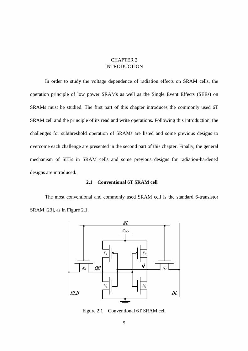
2.1 Conventional 6T SRAM cell
The most conventional and commonly used SRAM cell is the standard 6-transistor
SRAM [23], as in Figure 2.1.
Figure 2.1 Conventional 6T SRAM cell

6
The 6T cell contains a pair of cross-coupled inverters (P1, N1 and P2, N2) to secure
the states and a pair of access transistors (N3 and N4) driven by wordline (WL) and connected
to bitlines (BL and BLB) to read or write the state from the nodes Q and QB. The positive
feedback in the cross-coupled inverters corrects the disturbance of noise and leakage to
maintain the states. In order to ensure the functionality of the 6T SRAM cell, some
transistor-sizing constraints must be fulfilled.
2.1.1 Write Operation
To study the write operation of 6T cell, a simplified model of the 6T SRAM cell
during write operation is shown as Figure 2.2. It can be assumed that the initial state of the
cell is Q = ‘1’, and we wish to write ‘0’ to Q. BLB is driven to high and BL is pulled down to
low by the input driver. WL is asserted, turning both N3 and N4 on to open access to node Q
and QB. Note that Q must be pulled low enough to ensure reliable writing to the cell, that is,
below the threshold voltage Vtn of N3. Once Q falls below Vtn, P1 is turned on and N1 is
turned off, pulling QB high as desired. In order to satisfy this condition, the drivability of N4
must be bigger than P2. The pull-up ratio of the cell, PR, which is defined as the size ratio
between the PMOS and the access NMOS (naming P2 and N4),
2 2
4 4
/
/
P P
N N
W LPR
W L
must be
smaller than 1.8 [23]. Figure 2.3 illustrates the waveforms for the write operation. In
correspondence with the assumption above, ‘0’ is written into Q, which was initially ‘1’.
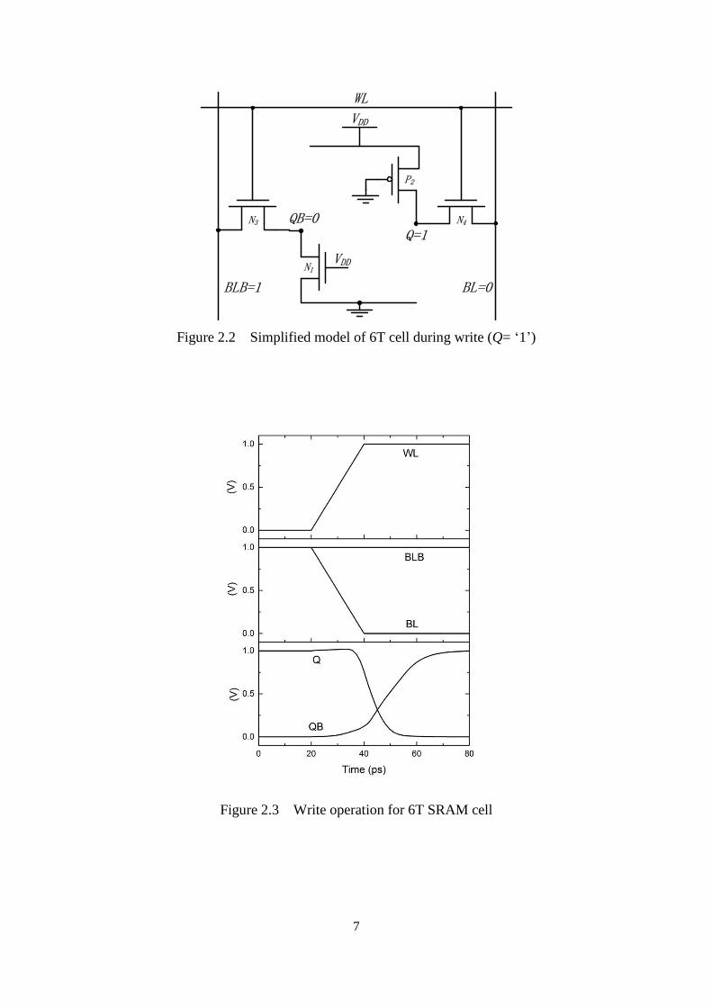
7
WL
VDD
P2
N1
N3 N4
Q=1QB=0
BLB=1 BL=0
VDD
Figure 2.2 Simplified model of 6T cell during write (Q= ‘1’)
Figure 2.3 Write operation for 6T SRAM cell
8
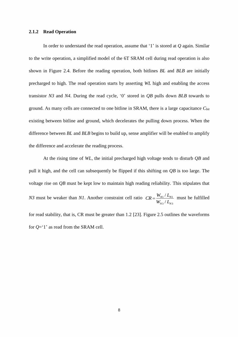
2.1.2 Read Operation
In order to understand the read operation, assume that ‘1’ is stored at Q again. Similar
to the write operation, a simplified model of the 6T SRAM cell during read operation is also
shown in Figure 2.4. Before the reading operation, both bitlines BL and BLB are initially
precharged to high. The read operation starts by asserting WL high and enabling the access
transistor N3 and N4. During the read cycle, ‘0’ stored in QB pulls down BLB towards to
ground. As many cells are connected to one bitline in SRAM, there is a large capacitance Cbit
existing between bitline and ground, which decelerates the pulling down process. When the
difference between BL and BLB begins to build up, sense amplifier will be enabled to amplify
the difference and accelerate the reading process.
At the rising time of WL, the initial precharged high voltage tends to disturb QB and
pull it high, and the cell can subsequently be flipped if this shifting on QB is too large. The
voltage rise on QB must be kept low to maintain high reading reliability. This stipulates that
N3 must be weaker than N1. Another constraint cell ratio 1 1
3 3
/
/
N N
N N
W LCR
W L must be fulfilled
for read stability, that is, CR must be greater than 1.2 [23]. Figure 2.5 outlines the waveforms
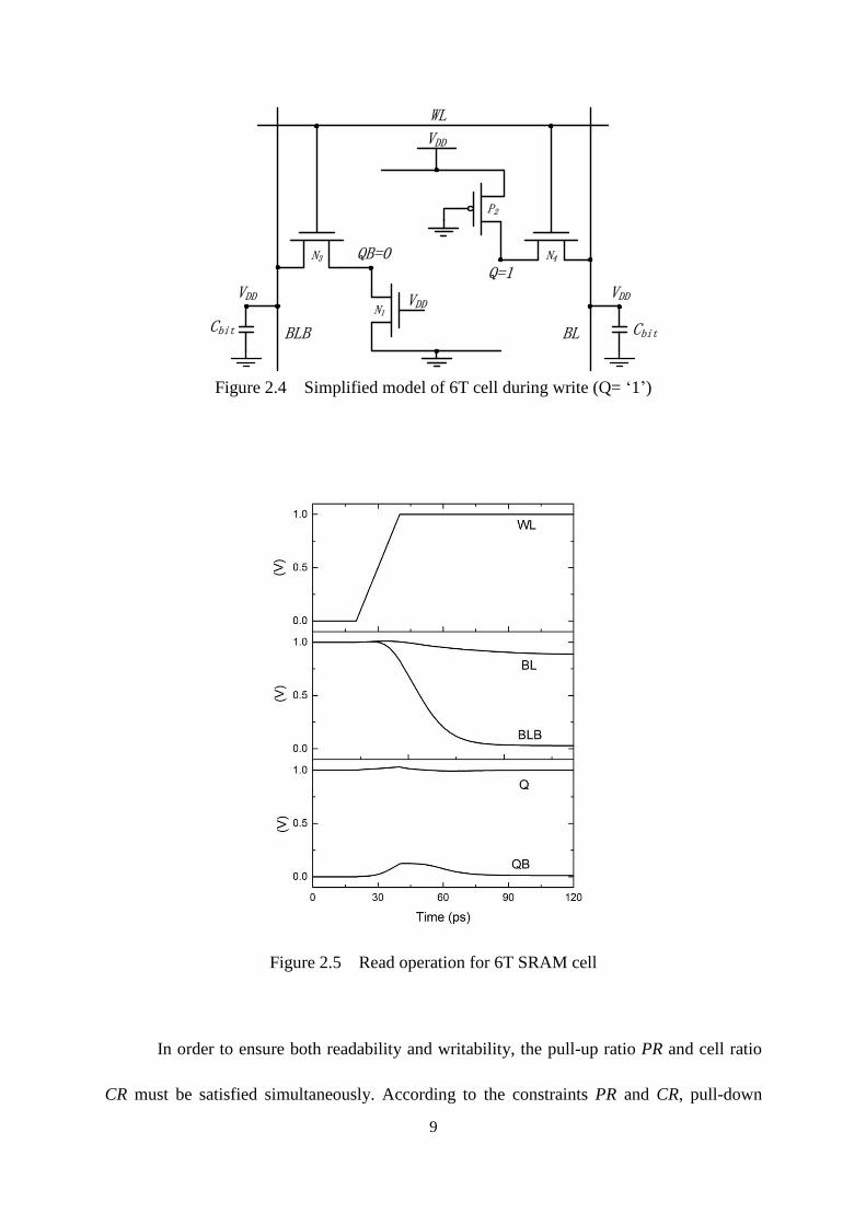
for Q=‘1’ as read from the SRAM cell.
9
WL
VDD
P2
N1
N3 N4
Q=1QB=0
BLB BL
VDDVDD VDD
Cbit Cbit
Figure 2.4 Simplified model of 6T cell during write (Q= ‘1’)
Figure 2.5 Read operation for 6T SRAM cell
In order to ensure both readability and writability, the pull-up ratio PR and cell ratio
CR must be satisfied simultaneously. According to the constraints PR and CR, pull-down
10
nmos N1 and N2 must be the strongest. Access transistors N3 and N4 should have medium
strength, and the pull-up PMOS must be the weakest. Meanwhile, all transistors must be as
small as possible in order to achieve higher layout density.
2.2 Challenges for Low Power Operation
2.2.1 Static Noise Margin
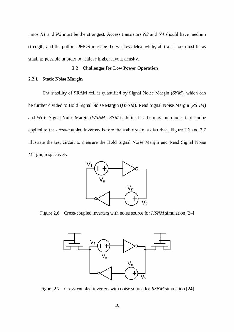
The stability of SRAM cell is quantified by Signal Noise Margin (SNM), which can
be further divided to Hold Signal Noise Margin (HSNM), Read Signal Noise Margin (RSNM)
and Write Signal Noise Margin (WSNM). SNM is defined as the maximum noise that can be
applied to the cross-coupled inverters before the stable state is disturbed. Figure 2.6 and 2.7
illustrate the test circuit to measure the Hold Signal Noise Margin and Read Signal Noise
Margin, respectively.
Vn
Vn
V1
V2
Figure 2.6 Cross-coupled inverters with noise source for HSNM simulation [24]
Vn
Vn
V1
V2
Figure 2.7 Cross-coupled inverters with noise source for RSNM simulation [24]

11
Figure 2.8 Butterfly diagram indicating HSNM
Figure 2.9 Butterfly diagram indicating RSNM
SNM can be determined from the butterfly diagrams as shown in Figure 2.8 and 2.9.
The butterfly curves are plotted by setting Vn=0, plotting V1 against V2 and V2 against V1,
respectively. SNM can be obtained by the size of maximum square inside the two
cross-coupled curves. As it can be seen, RSNM is significantly smaller than HSNM, as the
cross-coupled inverters are affected by the open access to VDD. RSNM is determined by the

12
cell ratio-CR; a higher CR increases the read margin in the trade off of taking more area for
the pull-down transistors N1 and N2. In this thesis, when we come to the term SNM, it is
referred to as RSNM.
Previous designs to improve the RSNM
Chang’s 8T cell
WWLVDD
P1 P2
N1 N2
N3N4Q
QB
BLB BL
RWL
RBL
N5
N6
Figure 2.10 Schematic of 8T SRAM cell [25]
An 8T SRAM cell providing separate reading and writing operation was proposed by
Chang [25] as in Figure 2.10. Two more transistors, N5 and N6, and one read wordline (RWL)
are added to 6T SRAM cell to improve the stability of the read operation. During the write
operation, RWL is turned low to ensure that N6 is off, blocking the path from group in order
to read bitline RWL. WWL, in turn, is set to high. Therefore, in terms of the write operation,
there is no difference between Chang’s 8T cell and the conventional 6T cell. For a read cycle,
assume data stored in the cell is ‘0’, that is Q= ‘0’ and QB= ‘1’. RWL is asserted to turn on
N6, while WWL keeps ‘0’ to turn off N3 and N4. N5 is also on as QB= ‘1’. In this case, an
open path from ground to RBL is constructed to pull RBL down. If cell content is ‘1’, that is
13
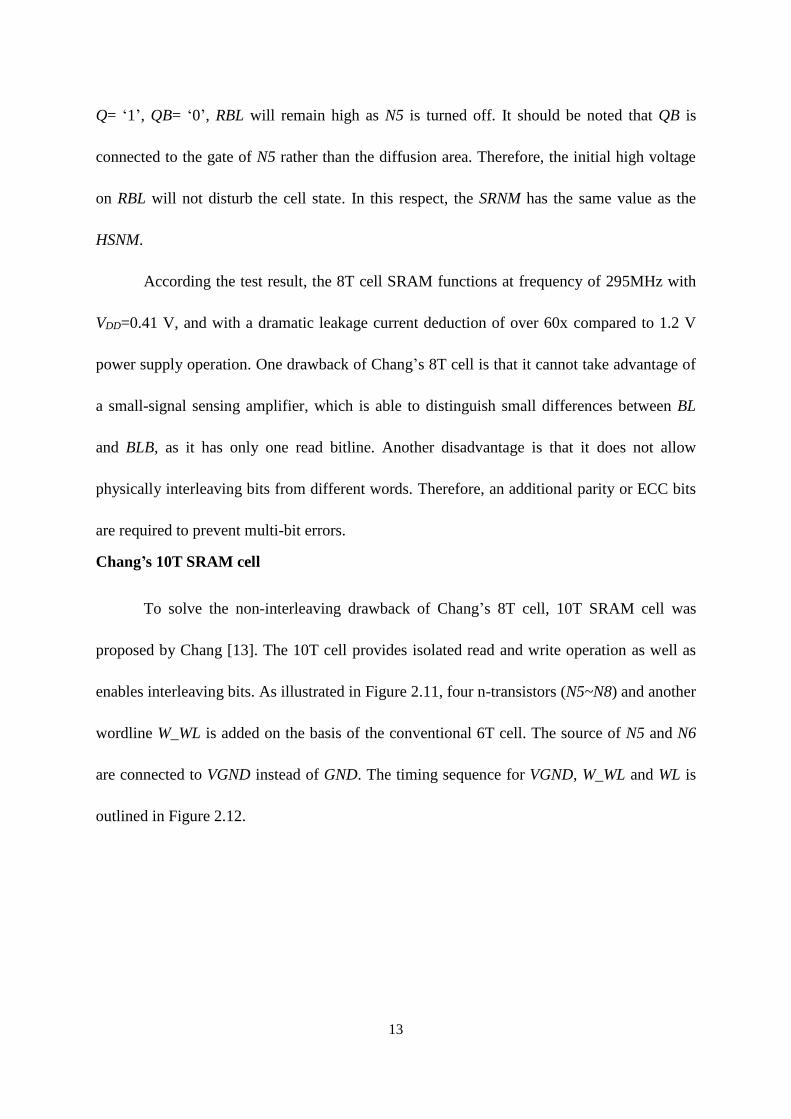
Q= ‘1’, QB= ‘0’, RBL will remain high as N5 is turned off. It should be noted that QB is
connected to the gate of N5 rather than the diffusion area. Therefore, the initial high voltage
on RBL will not disturb the cell state. In this respect, the SRNM has the same value as the
HSNM.
According the test result, the 8T cell SRAM functions at frequency of 295MHz with
VDD=0.41 V, and with a dramatic leakage current deduction of over 60x compared to 1.2 V
power supply operation. One drawback of Chang’s 8T cell is that it cannot take advantage of
a small-signal sensing amplifier, which is able to distinguish small differences between BL
and BLB, as it has only one read bitline. Another disadvantage is that it does not allow
physically interleaving bits from different words. Therefore, an additional parity or ECC bits
are required to prevent multi-bit errors.
Chang’s 10T SRAM cell
To solve the non-interleaving drawback of Chang’s 8T cell, 10T SRAM cell was
proposed by Chang [13]. The 10T cell provides isolated read and write operation as well as
enables interleaving bits. As illustrated in Figure 2.11, four n-transistors (N5~N8) and another
wordline W_WL is added on the basis of the conventional 6T cell. The source of N5 and N6
are connected to VGND instead of GND. The timing sequence for VGND, W_WL and WL is
outlined in Figure 2.12.
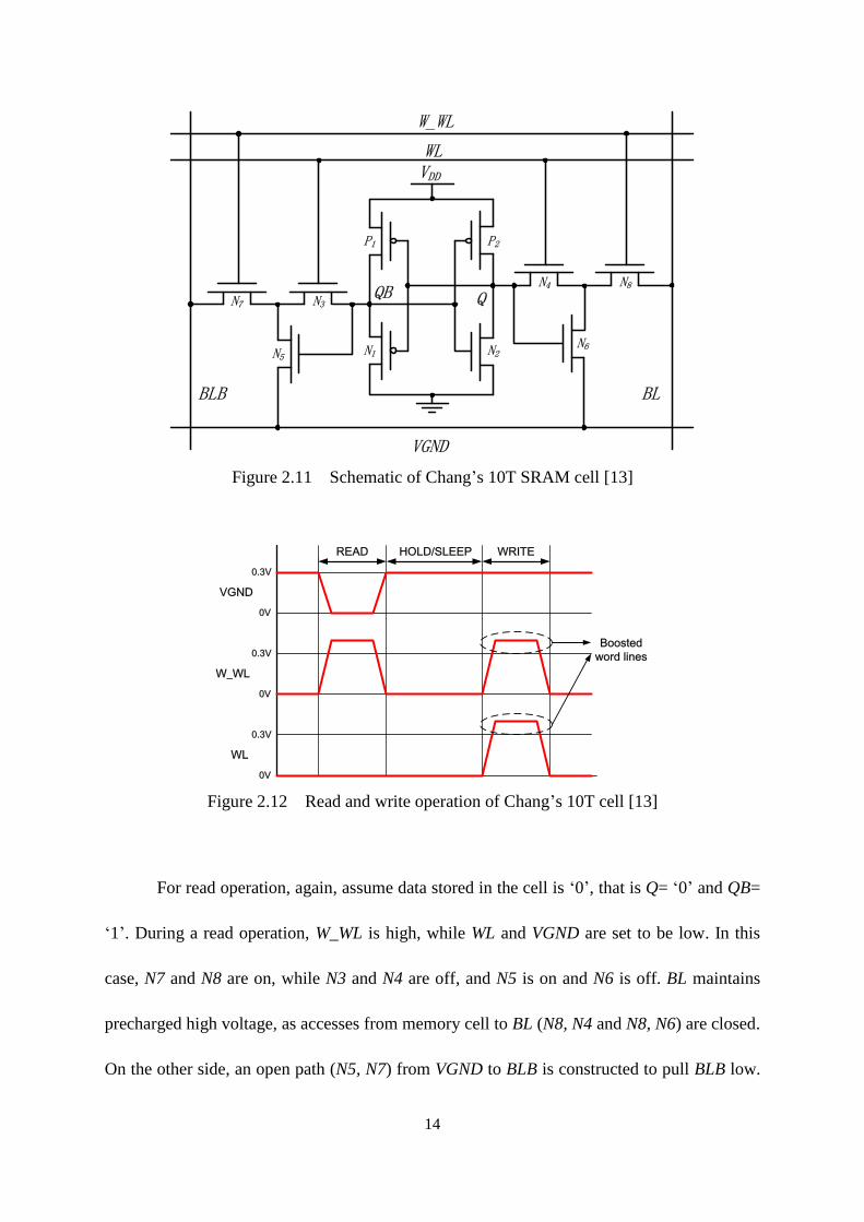
14
WLVDD
P1 P2
N1 N2
N3
N4QQB
BLB BL
W_WL
N5N6
N7
N8
VGND
Figure 2.11 Schematic of Chang’s 10T SRAM cell [13]
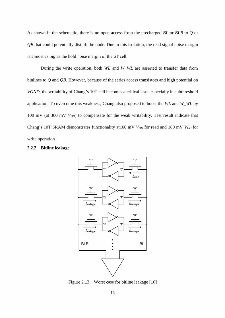
READ HOLD/SLEEP WRITE
VGND
W_WL
WL
0V
0.3V
0V
0.3V
0V
0.3V
Boosted
word lines
Figure 2.12 Read and write operation of Chang’s 10T cell [13]
For read operation, again, assume data stored in the cell is ‘0’, that is Q= ‘0’ and QB=
‘1’. During a read operation, W_WL is high, while WL and VGND are set to be low. In this
case, N7 and N8 are on, while N3 and N4 are off, and N5 is on and N6 is off. BL maintains
precharged high voltage, as accesses from memory cell to BL (N8, N4 and N8, N6) are closed.
On the other side, an open path (N5, N7) from VGND to BLB is constructed to pull BLB low.
15
As shown in the schematic, there is no open access from the precharged BL or BLB to Q or
QB that could potentially disturb the node. Due to this isolation, the read signal noise margin
is almost as big as the hold noise margin of the 6T cell.
During the write operation, both WL and W_WL are asserted to transfer data from
binlines to Q and QB. However, because of the series access transistors and high potential on
VGND, the writability of Chang’s 10T cell becomes a critical issue especially in subthreshold
application. To overcome this weakness, Chang also proposed to boost the WL and W_WL by
100 mV (at 300 mV VDD) to compensate for the weak writability. Test result indicate that
Chang’s 10T SRAM demonstrates functionality at160 mV VDD for read and 180 mV VDD for
write operation.
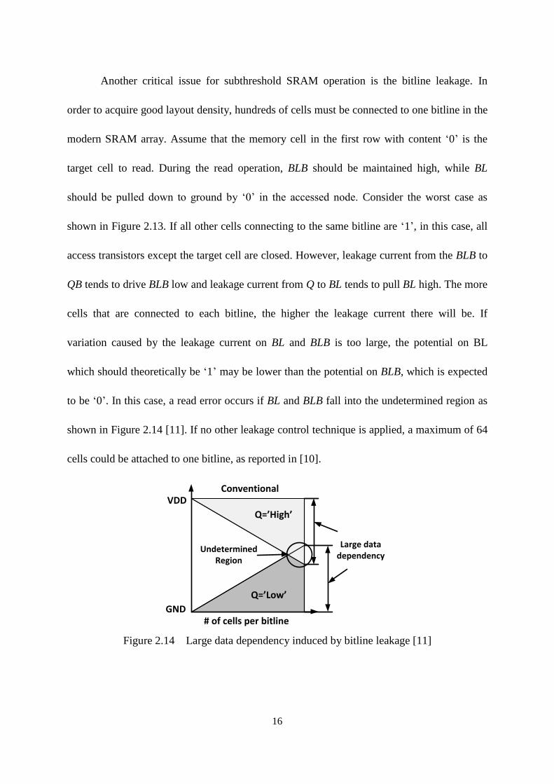
2.2.2 Bitline leakage
“1” “1”
“1” “0”
“0” “0”
“0” “1”
“0” “0”
“0” “1”
BLBLB
Iread
Ileakage Ileakage
Ileakage Ileakage
Figure 2.13 Worst case for bitline leakage [10]
16
Another critical issue for subthreshold SRAM operation is the bitline leakage. In
order to acquire good layout density, hundreds of cells must be connected to one bitline in the
modern SRAM array. Assume that the memory cell in the first row with content ‘0’ is the
target cell to read. During the read operation, BLB should be maintained high, while BL
should be pulled down to ground by ‘0’ in the accessed node. Consider the worst case as
shown in Figure 2.13. If all other cells connecting to the same bitline are ‘1’, in this case, all
access transistors except the target cell are closed. However, leakage current from the BLB to
QB tends to drive BLB low and leakage current from Q to BL tends to pull BL high. The more
cells that are connected to each bitline, the higher the leakage current there will be. If
variation caused by the leakage current on BL and BLB is too large, the potential on BL
which should theoretically be ‘1’ may be lower than the potential on BLB, which is expected
to be ‘0’. In this case, a read error occurs if BL and BLB fall into the undetermined region as
shown in Figure 2.14 [11]. If no other leakage control technique is applied, a maximum of 64
cells could be attached to one bitline, as reported in [10].
ConventionalVDD
# of cells per bitlineGND
UndeterminedRegion
Large datadependency
Q=’High’
Q=’Low’
Figure 2.14 Large data dependency induced by bitline leakage [11]
17
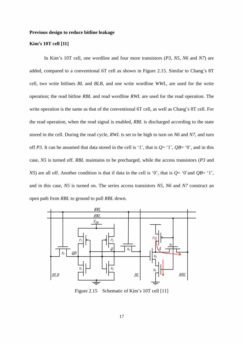
Previous design to reduce bitline leakage
Kim’s 10T cell [11]
In Kim’s 10T cell, one wordline and four more transistors (P3, N5, N6 and N7) are
added, compared to a conventional 6T cell as shown in Figure 2.15. Similar to Chang’s 8T
cell, two write bitlines BL and BLB, and one write wordline WWL, are used for the write
operation; the read bitline RBL and read wordline RWL are used for the read operation. The
write operation is the same as that of the conventional 6T cell, as well as Chang’s 8T cell. For
the read operation, when the read signal is enabled, RBL is discharged according to the state
stored in the cell. During the read cycle, RWL is set to be high to turn on N6 and N7, and turn
off P3. It can be assumed that data stored in the cell is ‘1’, that is Q= ‘1’, QB= ‘0’, and in this
case, N5 is turned off. RBL maintains to be precharged, while the access transistors (P3 and
N5) are all off. Another condition is that if data in the cell is ‘0’, that is Q= ‘0’and QB= ‘1’,
and in this case, N5 is turned on. The series access transistors N5, N6 and N7 construct an
open path from RBL to ground to pull RBL down.
WWL
VDD
P1 P2
N1 N2
N3N4Q
QB
BLB BL RBL
RWL
N6
N5
N7
P3
A
Figure 2.15 Schematic of Kim’s 10T cell [11]
18
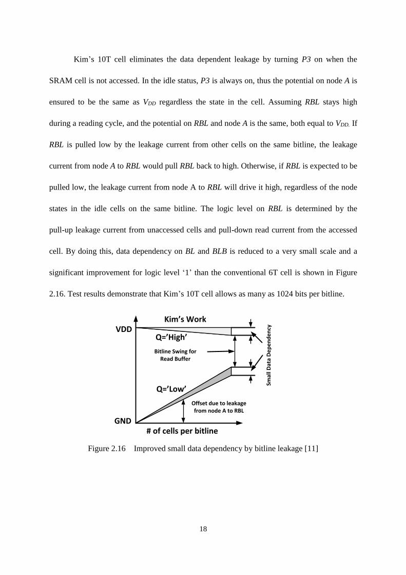
Kim’s 10T cell eliminates the data dependent leakage by turning P3 on when the
SRAM cell is not accessed. In the idle status, P3 is always on, thus the potential on node A is
ensured to be the same as VDD regardless the state in the cell. Assuming RBL stays high
during a reading cycle, and the potential on RBL and node A is the same, both equal to VDD. If
RBL is pulled low by the leakage current from other cells on the same bitline, the leakage
current from node A to RBL would pull RBL back to high. Otherwise, if RBL is expected to be
pulled low, the leakage current from node A to RBL will drive it high, regardless of the node
states in the idle cells on the same bitline. The logic level on RBL is determined by the
pull-up leakage current from unaccessed cells and pull-down read current from the accessed
cell. By doing this, data dependency on BL and BLB is reduced to a very small scale and a
significant improvement for logic level ‘1’ than the conventional 6T cell is shown in Figure
2.16. Test results demonstrate that Kim’s 10T cell allows as many as 1024 bits per bitline.
Kim’s WorkVDD
# of cells per bitlineGND
Bitline Swing for Read Buffer
Smal
l Dat
a D
ep
en
de
ncy
Q=’High’
Q=’Low’
Offset due to leakage from node A to RBL
Figure 2.16 Improved small data dependency by bitline leakage [11]
19
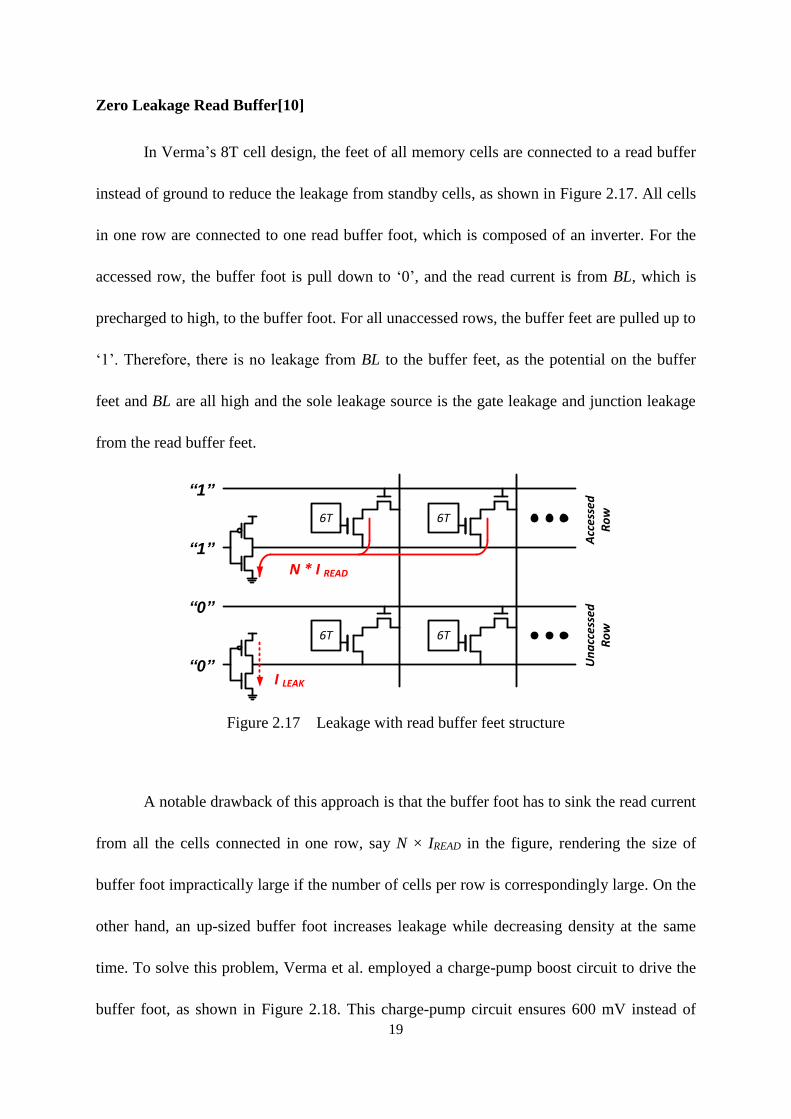
Zero Leakage Read Buffer[10]
In Verma’s 8T cell design, the feet of all memory cells are connected to a read buffer
instead of ground to reduce the leakage from standby cells, as shown in Figure 2.17. All cells
in one row are connected to one read buffer foot, which is composed of an inverter. For the
accessed row, the buffer foot is pull down to ‘0’, and the read current is from BL, which is
precharged to high, to the buffer foot. For all unaccessed rows, the buffer feet are pulled up to
‘1’. Therefore, there is no leakage from BL to the buffer feet, as the potential on the buffer
feet and BL are all high and the sole leakage source is the gate leakage and junction leakage
from the read buffer feet.
6T
6T
6T
6T
“1”
“0”
“1”
“0”
N * I READ
I LEAK
Acc
esse
d
Ro
wU
na
cces
sed
R
ow
Figure 2.17 Leakage with read buffer feet structure
A notable drawback of this approach is that the buffer foot has to sink the read current
from all the cells connected in one row, say N × IREAD in the figure, rendering the size of
buffer foot impractically large if the number of cells per row is correspondingly large. On the
other hand, an up-sized buffer foot increases leakage while decreasing density at the same
time. To solve this problem, Verma et al. employed a charge-pump boost circuit to drive the
buffer foot, as shown in Figure 2.18. This charge-pump circuit ensures 600 mV instead of
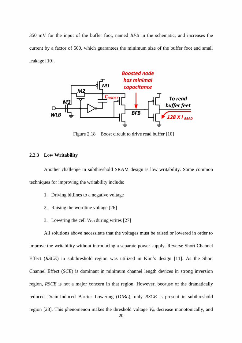
20
350 mV for the input of the buffer foot, named BFB in the schematic, and increases the
current by a factor of 500, which guarantees the minimum size of the buffer foot and small
leakage [10].
128 X I READ
Boosted node has minimal capacitance
To read buffer feet
BFB
CBOOST
M1M2
M3
WLB
Figure 2.18 Boost circuit to drive read buffer [10]
2.2.3 Low Writability
Another challenge in subthreshold SRAM design is low writability. Some common
techniques for improving the writability include:
1. Driving bitlines to a negative voltage
2. Raising the wordline voltage [26]
3. Lowering the cell VDD during writes [27]
All solutions above necessitate that the voltages must be raised or lowered in order to
improve the writability without introducing a separate power supply. Reverse Short Channel
Effect (RSCE) in subthreshold region was utilized in Kim’s design [11]. As the Short
Channel Effect (SCE) is dominant in minimum channel length devices in strong inversion
region, RSCE is not a major concern in that region. However, because of the dramatically
reduced Drain-Induced Barrier Lowering (DIBL), only RSCE is present in subthreshold
region [28]. This phenomenon makes the threshold voltage Vth decrease monotonically, and
21
the operation current increases exponentially as the channel length is longer. Simulation with
a 130 nm technology demonstrates that, when VDD=1.2 V, the maximum current through
transistors decreases as the channel length increases. However, when VDD reduces to 0.2 V,
RSCE becomes dominant and the maximum current through the transistor occurs when
channel length equals to 0.55 um instead of 0.13 um in the 130 nm technology.
2.3 Fault-tolerant Design
2.3.1 Single Event Upset
SEEs, caused by an energetic particle that penetrates sensitive nodes in IC materials,
can lead to a plethora of adverse effects, from minor system responses to catastrophic system
failures. A Single Event Upset (SEU) is a state change of storage cells caused by SEEs,
which is a non-destructive soft error. In contrast to other circuits, memory cells can
“remember” this kind of errors and the functionality of the whole system may eventually be
affected. Therefore, SEUs must be carefully considered, especially for space applications
where cosmic rays and high-energy ions are commonly present. When travelling to the
earth’s surface through the atmosphere, most of the cosmic rays and ions are trapped.
However, a small amount of particles are able to penetrate the atmosphere and reach the
surface of the earth. If high reliability is required, SEUs must also be taken into
consideration.
22
n+
Ion track
p-sub
n+
Idrift
n+
p-subp-sub
Idrift
(a) (b) (c)
Figure 2.19 Mechanism of Single Event Effect [29]
Figure 2.20 Single Event Effect current [29]
The mechanism for an SEE triggered by an ion track is as shown in Figure 2.19. At
the time a heavy ion strikes through the diffusion area, a high concentration of electron-hole
pairs is formed by the ionization effect (a). When the resultant track of carriers pass or get
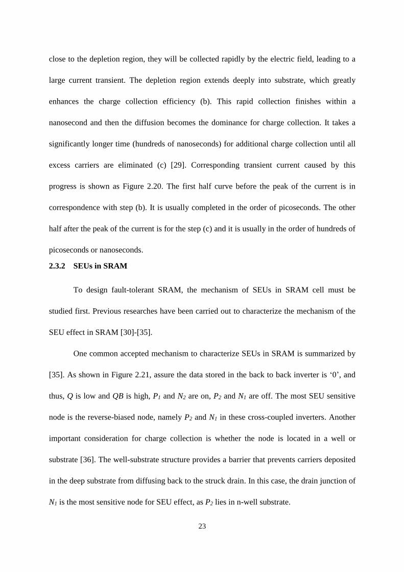
23
close to the depletion region, they will be collected rapidly by the electric field, leading to a
large current transient. The depletion region extends deeply into substrate, which greatly
enhances the charge collection efficiency (b). This rapid collection finishes within a
nanosecond and then the diffusion becomes the dominance for charge collection. It takes a
significantly longer time (hundreds of nanoseconds) for additional charge collection until all
excess carriers are eliminated (c) [29]. Corresponding transient current caused by this
progress is shown as Figure 2.20. The first half curve before the peak of the current is in
correspondence with step (b). It is usually completed in the order of picoseconds. The other
half after the peak of the current is for the step (c) and it is usually in the order of hundreds of
picoseconds or nanoseconds.
2.3.2 SEUs in SRAM
To design fault-tolerant SRAM, the mechanism of SEUs in SRAM cell must be
studied first. Previous researches have been carried out to characterize the mechanism of the
SEU effect in SRAM [30]-[35].
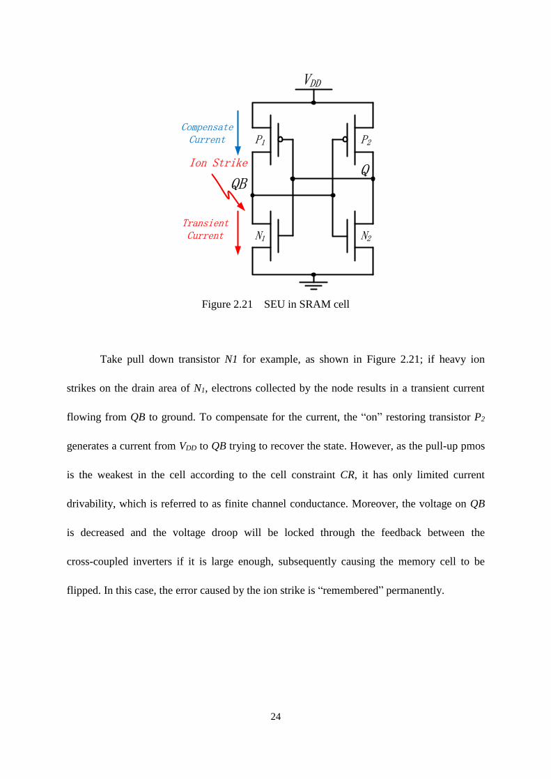
One common accepted mechanism to characterize SEUs in SRAM is summarized by
[35]. As shown in Figure 2.21, assure the data stored in the back to back inverter is ‘0’, and
thus, Q is low and QB is high, P1 and N2 are on, P2 and N1 are off. The most SEU sensitive
node is the reverse-biased node, namely P2 and N1 in these cross-coupled inverters. Another
important consideration for charge collection is whether the node is located in a well or
substrate [36]. The well-substrate structure provides a barrier that prevents carriers deposited
in the deep substrate from diffusing back to the struck drain. In this case, the drain junction of
N1 is the most sensitive node for SEU effect, as P2 lies in n-well substrate.
24
VDD
P1 P2
N1 N2
QQB
Ion Strike
Transient Current
CompensateCurrent
Figure 2.21 SEU in SRAM cell
Take pull down transistor N1 for example, as shown in Figure 2.21; if heavy ion
strikes on the drain area of N1, electrons collected by the node results in a transient current
flowing from QB to ground. To compensate for the current, the “on” restoring transistor P2
generates a current from VDD to QB trying to recover the state. However, as the pull-up pmos
is the weakest in the cell according to the cell constraint CR, it has only limited current
drivability, which is referred to as finite channel conductance. Moreover, the voltage on QB
is decreased and the voltage droop will be locked through the feedback between the
cross-coupled inverters if it is large enough, subsequently causing the memory cell to be
flipped. In this case, the error caused by the ion strike is “remembered” permanently.
25
2.3.3 Radiation Tolerant SRAM Design
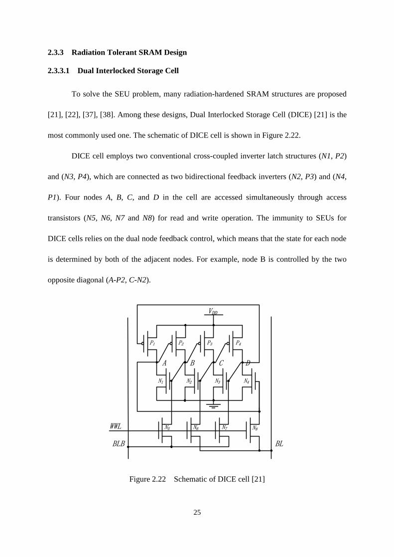
2.3.3.1 Dual Interlocked Storage Cell
To solve the SEU problem, many radiation-hardened SRAM structures are proposed
[21], [22], [37], [38]. Among these designs, Dual Interlocked Storage Cell (DICE) [21] is the
most commonly used one. The schematic of DICE cell is shown in Figure 2.22.
DICE cell employs two conventional cross-coupled inverter latch structures (N1, P2)
and (N3, P4), which are connected as two bidirectional feedback inverters (N2, P3) and (N4,
P1). Four nodes A, B, C, and D in the cell are accessed simultaneously through access
transistors (N5, N6, N7 and N8) for read and write operation. The immunity to SEUs for
DICE cells relies on the dual node feedback control, which means that the state for each node
is determined by both of the adjacent nodes. For example, node B is controlled by the two
opposite diagonal (A-P2, C-N2).
WWL
VDD
N1
P1
BLB BL
N2 N3 N4
P2 P3 P4
N5 N6 N7 N8
A B C D
Figure 2.22 Schematic of DICE cell [21]
26
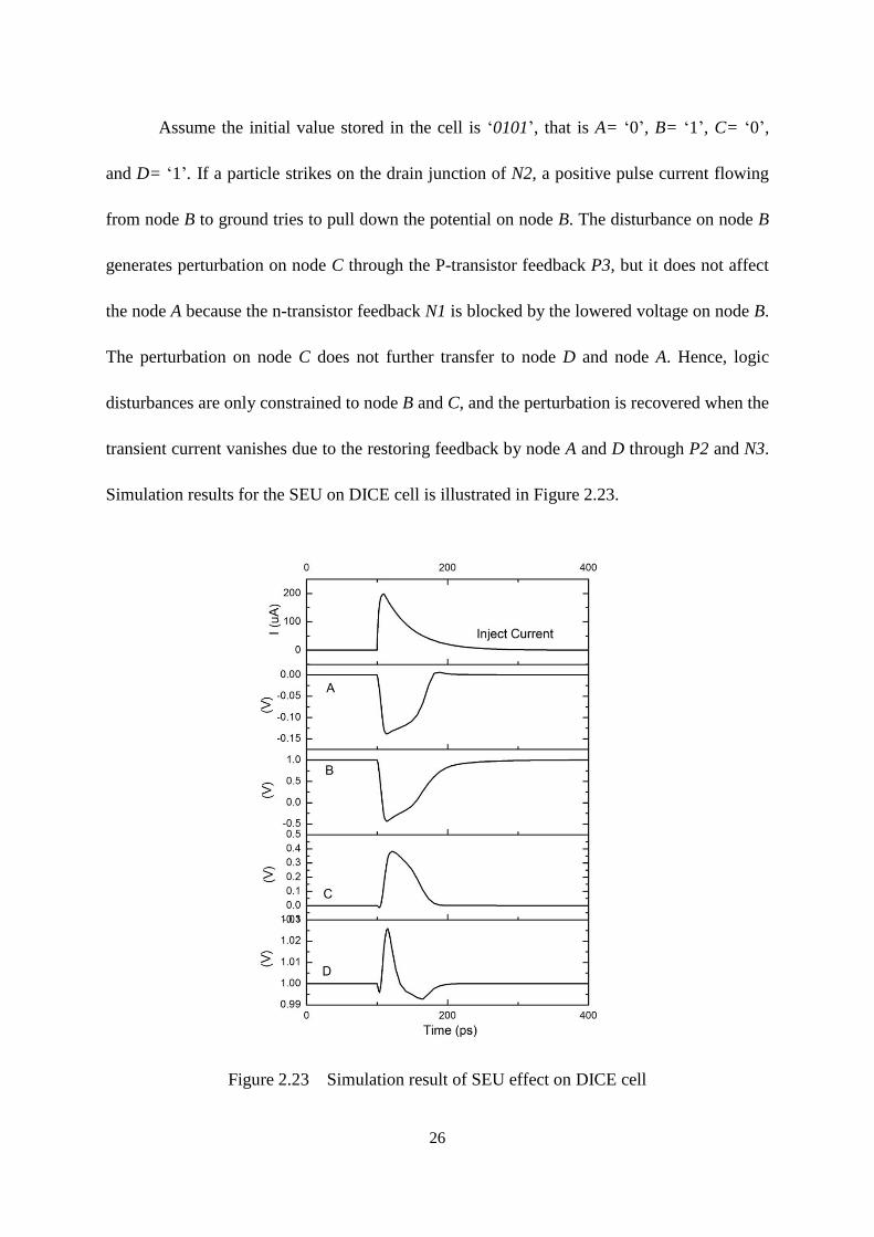
Assume the initial value stored in the cell is ‘0101’, that is A= ‘0’, B= ‘1’, C= ‘0’,
and D= ‘1’. If a particle strikes on the drain junction of N2, a positive pulse current flowing
from node B to ground tries to pull down the potential on node B. The disturbance on node B
generates perturbation on node C through the P-transistor feedback P3, but it does not affect
the node A because the n-transistor feedback N1 is blocked by the lowered voltage on node B.
The perturbation on node C does not further transfer to node D and node A. Hence, logic
disturbances are only constrained to node B and C, and the perturbation is recovered when the
transient current vanishes due to the restoring feedback by node A and D through P2 and N3.
Simulation results for the SEU on DICE cell is illustrated in Figure 2.23.
Figure 2.23 Simulation result of SEU effect on DICE cell

27
Simulation and experimental results prove that DICE cell can recover from any upset as long
as only one sensitive node is affected no matter how large the particle energy is. However, if
two sensitive nodes with same logic state are hit simultaneously (A and C or B and D), the
immunity is lost and the cell can be flipped. The chance of multi-node upset is very small and
charge sharing is not a critical issue when the feature size of transistors is large, which is the
case for less advanced technologies. However, with the technology scaling down, multi-node
error becomes more serious as the charge generated by one hit might be shared by multiple
nodes as the transistors size and space are both small.
2.3.3.2 Quatro cell
WL
VDD
P1
P2
N1
N2
N6 N5
AB
BLB BL
N3
N4
P3
P4
CD
Figure 2.24 Schematic of Quatro cell [22]
Jahinuzzaman et al. proposed a 10-transistor radiation tolerance SRAM cell in 2009,
as shown in Figure 2.24 [22]. Two access transistors (N5 and N6) are connected to the storage
cell A and B. The four nodes A, B, C and D are all driven by a pmos and nmos transistor, and
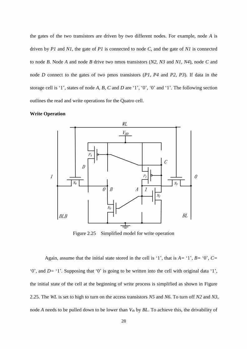
28
the gates of the two transistors are driven by two different nodes. For example, node A is
driven by P1 and N1, the gate of P1 is connected to node C, and the gate of N1 is connected
to node B. Node A and node B drive two nmos transistors (N2, N3 and N1, N4), node C and
node D connect to the gates of two pmos transistors (P1, P4 and P2, P3). If data in the
storage cell is ‘1’, states of node A, B, C and D are ‘1’, ‘0’, ‘0’ and ‘1’. The following section
outlines the read and write operations for the Quatro cell.
Write Operation
WL
VDD
P1
N2
N6 N5
AB
BLB BL
N3
P4
CD
0
1
1
0
Figure 2.25 Simplified model for write operation
Again, assume that the initial state stored in the cell is ‘1’, that is A= ‘1’, B= ‘0’, C=
‘0’, and D= ‘1’. Supposing that ‘0’ is going to be written into the cell with original data ‘1’,
the initial state of the cell at the beginning of write process is simplified as shown in Figure
2.25. The WL is set to high to turn on the access transistors N5 and N6. To turn off N2 and N3,
node A needs to be pulled down to be lower than Vth by BL. To achieve this, the drivability of
29
P1 must be weaker than N5, as the carrier mobility of nmos is higher. Pull up ratio PR1,
which is defined as 1 1
5 5
/
/
P P
N N
W L
W L, can be 1 to pull node A down below Vth. Node B is pulled up
to Vth by BLB to turn on N3 and accelerate the pulling down of node A. To finish the write
process, node D must be lower than VDD-Vth to turn on P2 and P3, and thus, N4 must be
strong enough to fight against P4. Pull up ratio PR2, which is defined as 4 4
4 4
/
/
P P
N N
W L
W L , should
be 0.75 or smaller in order for this operation to be completed reliably. Simulation waveforms
of a write cycle are shown in Figure 2.26.
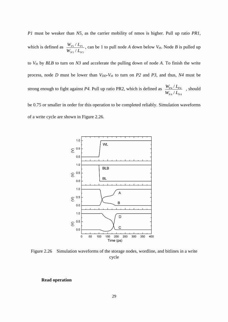
Figure 2.26 Simulation waveforms of the storage nodes, wordline, and bitlines in a write
cycle
Read operation
30
In the read operation, assume data stored in the cell is ‘1’, that is A= ‘1’ and B= ‘0’.
The simplified model for the initial state during a read cycle is the same as in Figure 2.27.
BLB is driven low by node B through the access transistor N6. For a stable read operation, the
pull down nmos transistor N3 must be stronger than the access transistor N6 to ensure node B
is not flipped by the precharged high voltage on BLB. The typical value for the aspect ratio
defined as 66
33
/
/
NN
NN
LW
LW is 1.5 ~ 1.7 for a safe read noise margin. Simulation waveforms of a
read cycle are illustrated in Figure 2.28.
WL
VDD
P1
N2
N6 N5
AB
BLB BL
N3
P4
CD
1
1
1
1
0
0
Figure 2.27 Simplified model for a write operation
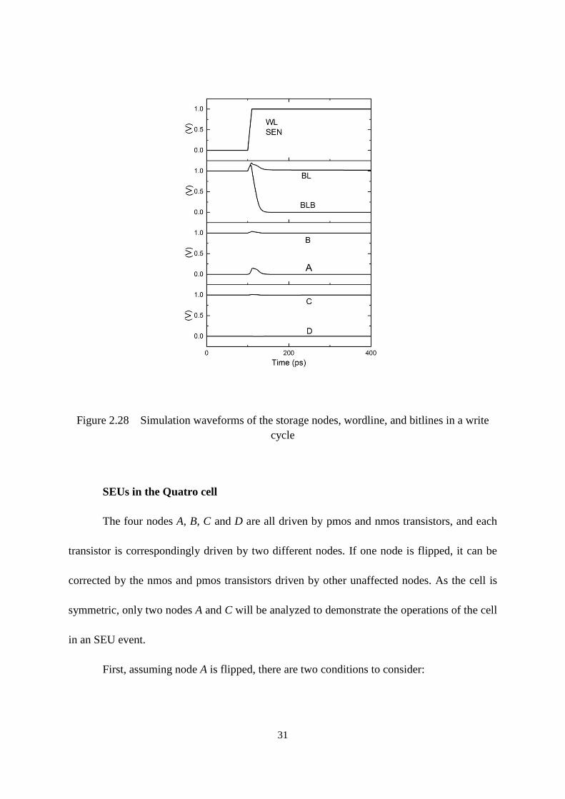
31
Figure 2.28 Simulation waveforms of the storage nodes, wordline, and bitlines in a write
cycle
SEUs in the Quatro cell
The four nodes A, B, C and D are all driven by pmos and nmos transistors, and each
transistor is correspondingly driven by two different nodes. If one node is flipped, it can be
corrected by the nmos and pmos transistors driven by other unaffected nodes. As the cell is
symmetric, only two nodes A and C will be analyzed to demonstrate the operations of the cell
in an SEU event.
First, assuming node A is flipped, there are two conditions to consider:
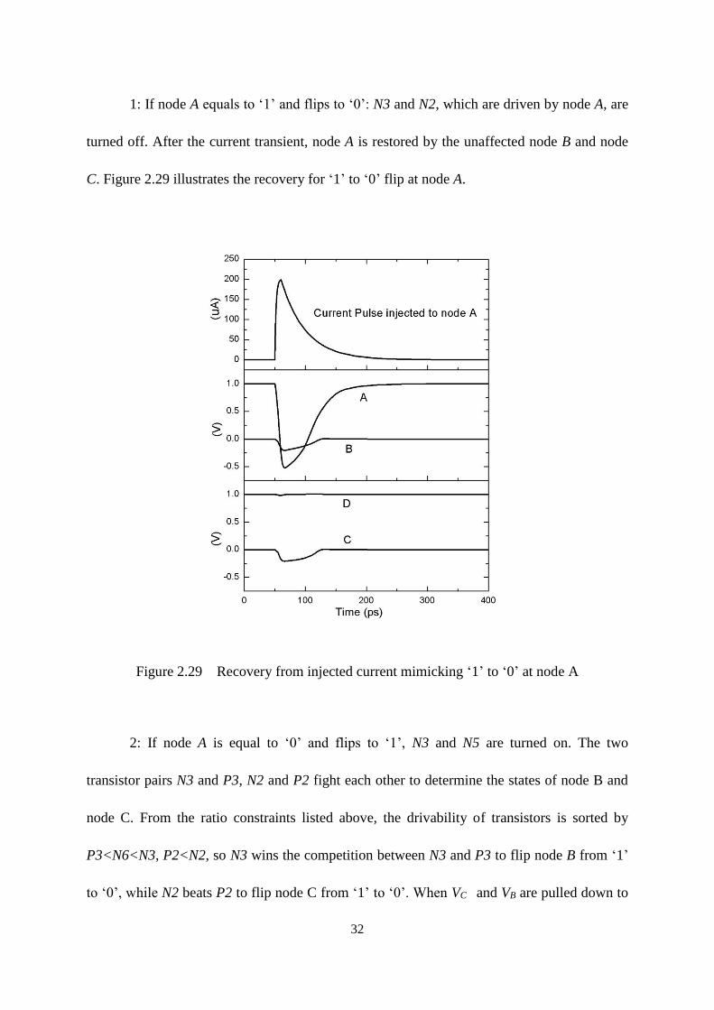
32
1: If node A equals to ‘1’ and flips to ‘0’: N3 and N2, which are driven by node A, are
turned off. After the current transient, node A is restored by the unaffected node B and node
C. Figure 2.29 illustrates the recovery for ‘1’ to ‘0’ flip at node A.
Figure 2.29 Recovery from injected current mimicking ‘1’ to ‘0’ at node A
2: If node A is equal to ‘0’ and flips to ‘1’, N3 and N5 are turned on. The two
transistor pairs N3 and P3, N2 and P2 fight each other to determine the states of node B and
node C. From the ratio constraints listed above, the drivability of transistors is sorted by
P3<N6<N3, P2<N2, so N3 wins the competition between N3 and P3 to flip node B from ‘1’
to ‘0’, while N2 beats P2 to flip node C from ‘1’ to ‘0’. When VC and VB are pulled down to
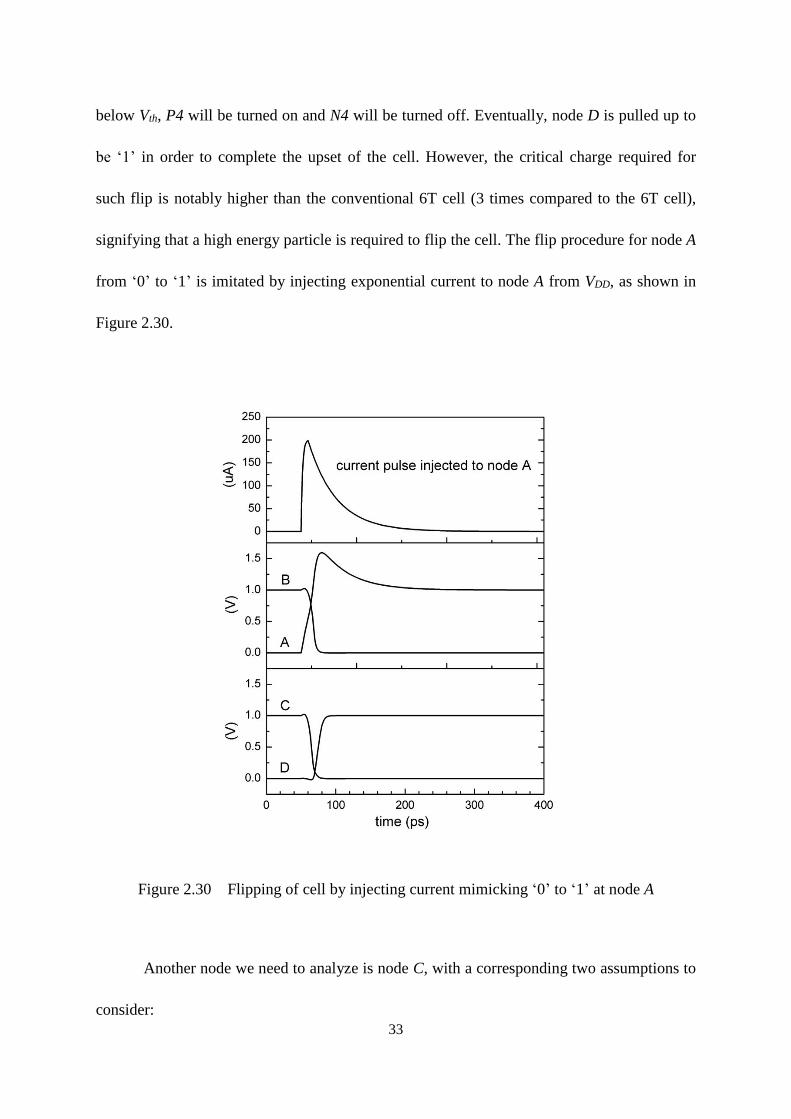
33
below Vth, P4 will be turned on and N4 will be turned off. Eventually, node D is pulled up to
be ‘1’ in order to complete the upset of the cell. However, the critical charge required for
such flip is notably higher than the conventional 6T cell (3 times compared to the 6T cell),
signifying that a high energy particle is required to flip the cell. The flip procedure for node A
from ‘0’ to ‘1’ is imitated by injecting exponential current to node A from VDD, as shown in
Figure 2.30.
Figure 2.30 Flipping of cell by injecting current mimicking ‘0’ to ‘1’ at node A
Another node we need to analyze is node C, with a corresponding two assumptions to
consider:
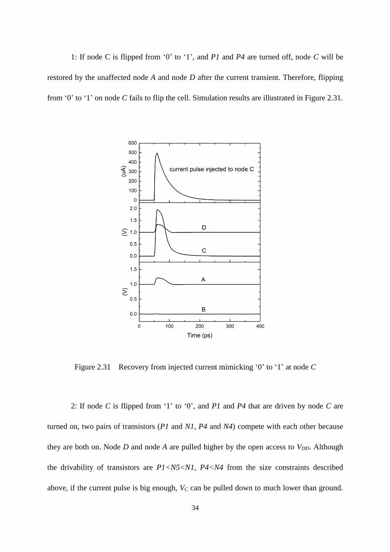
34
1: If node C is flipped from ‘0’ to ‘1’, and P1 and P4 are turned off, node C will be
restored by the unaffected node A and node D after the current transient. Therefore, flipping
from ‘0’ to ‘1’ on node C fails to flip the cell. Simulation results are illustrated in Figure 2.31.
Figure 2.31 Recovery from injected current mimicking ‘0’ to ‘1’ at node C
2: If node C is flipped from ‘1’ to ‘0’, and P1 and P4 that are driven by node C are
turned on, two pairs of transistors (P1 and N1, P4 and N4) compete with each other because
they are both on. Node D and node A are pulled higher by the open access to VDD. Although
the drivability of transistors are P1<N5<N1, P4<N4 from the size constraints described
above, if the current pulse is big enough, VC can be pulled down to much lower than ground.
35
In this case, VA and VD can be pulled up above Vth. If VA and VD are higher than Vth, N3 is
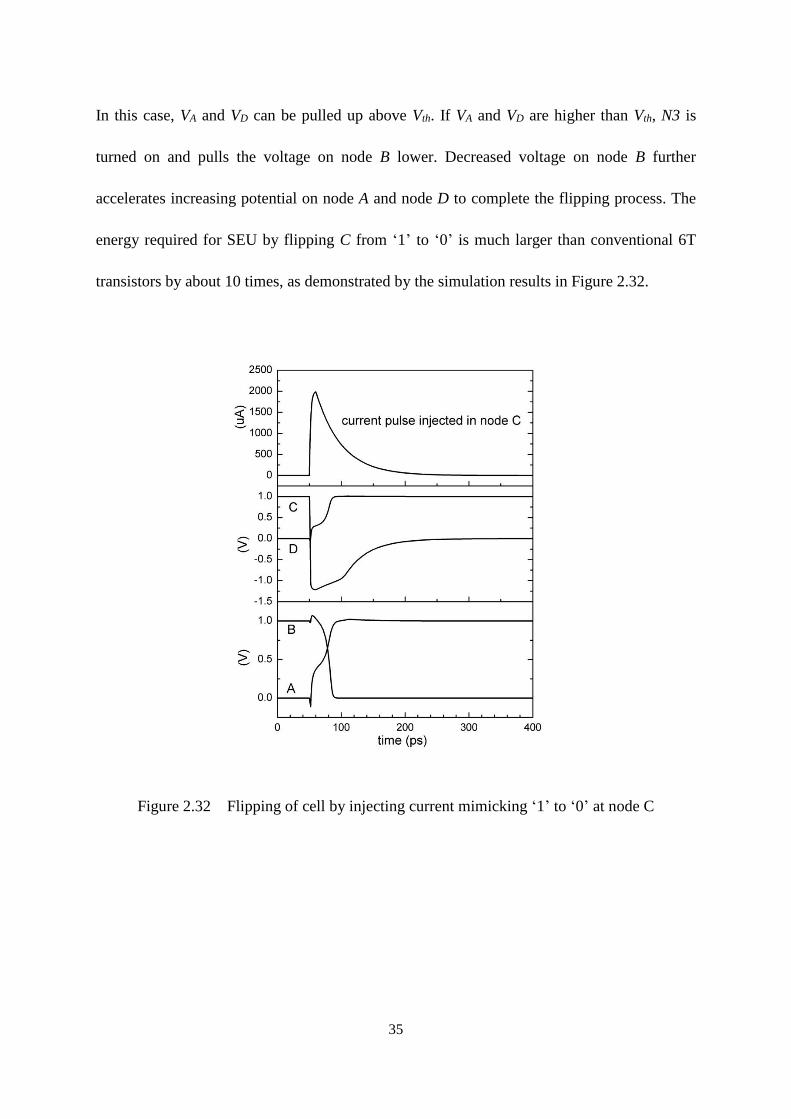
turned on and pulls the voltage on node B lower. Decreased voltage on node B further
accelerates increasing potential on node A and node D to complete the flipping process. The
energy required for SEU by flipping C from ‘1’ to ‘0’ is much larger than conventional 6T
transistors by about 10 times, as demonstrated by the simulation results in Figure 2.32.
Figure 2.32 Flipping of cell by injecting current mimicking ‘1’ to ‘0’ at node C
36
CHAPTER 3
SRAM DESIGN
In order to explore the power supply voltage dependence of heavy ion induced SEUs,
a full custom designed 16Kb SRAM test chip with four types of SRAM arrays was designed
and fabricated in a 65nm, 9-metal technology. Among the four cells, 6T and 10T are chosen
as unhardened cells, while Quatro and DICE are chosen as hardened ones to study their SERs
at various power supply voltages. This chapter will introduce the SRAM design and
configuration.
3.1 Memory Design Overview
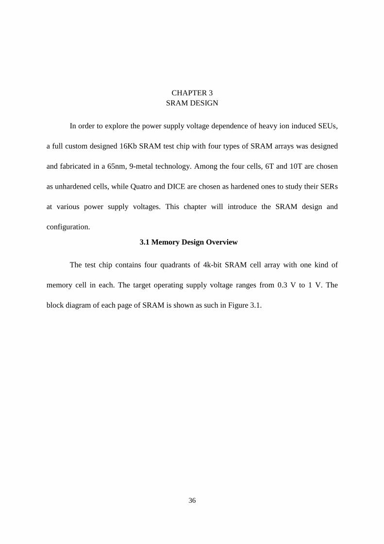
The test chip contains four quadrants of 4k-bit SRAM cell array with one kind of
memory cell in each. The target operating supply voltage ranges from 0.3 V to 1 V. The
block diagram of each page of SRAM is shown as such in Figure 3.1.

37
RO
W D
ECO
DER
CO
LUM
N 1
CO
LUM
N 2
CO
LUM
N 3
CO
LUM
N 4
CO
LUM
N 5
CO
LUM
N 6
CO
LUM
N 7
CO
LUM
N 8
SEQU
ENC
E C
ON
TRO
L
SA
DATA_IN
DATA_OUT
WC
CO
LUM
N
DEC
OD
ER
MUX
WC WC WC WC WC WC WC
SA SA SA SA SA SA SA
DATA0-DATA7
A6-A8
A0-A5
CLK
WR
RD
A6-A8
DOUT0-DOUT7
Figure 3.1 The block diagram for one page of the SRAM test chip
Each SRAM page contains eight columns of memory cell arrays, row decoder,
column decoder, sequence control circuit, write circuit, sense amplifier (SA) and multiplexer
(MUX). There are six inputs (A0 ~ A5) for the row decoder, three inputs (A6 ~ A8) for the
column decoder, 8-bit inputs (DATA0 ~ DATA7), 8-bit outputs (DOUT0 ~ DOUT7), clock
(CLK), read enable (RD), and write enable (WR) signals. The corresponding functions are
listed as follows.
Cell Array: The cell array contains eight columns with 64 bytes in each column,
which makes 512×8 bits in one array. There are sixth-four cells connected to one bitline to
reduce bitline leakage.
38
Row Decoder: A six to sixth-four row decoder is used to decode the lower six address
bits (A0 ~ A5) to turn on the wordline of the selected row and turn off the wordline of all
other unselected rows. There is one output (WL) or two outputs (RWL and WWL) for each
output of the row decoder, depending on the structure of the memory cells.
Column Decoder: A three to eight column decoder is employed to interpret the higher
three address bits (A6 ~ A8), enabling the column in which the target cell resides.
Sequence Control Circuit: It synchronizes all input signals, including RD, WR,
address signals (A0 ~ A8) and input data (DATA0 ~ DATA7) by the clock signal. Read enable
signal (RD) and write enable signal (WR) are all active low. It also generates all the other
timing sequence signals needed for the read and write circuit.
Sense Amplifier: The dynamic latch-type sense amplifier with differential inputs is
employed to distinguish and amplify the small swing of two bitlines to obtain the output
quickly and accurately.
Write circuit: It receives the input data from input IOs and drives BL or BLB to
complementary values to write into the memory cells.
Multiplex: Eight multiplexes decode the higher three address bits (A6 ~ A8), choosing
the output from eight columns to output IOs.
3.2 Memory Cells and Peripheral Circuits Design
This chapter will provide detailed design information for each part aforementioned in
the previous section.
39
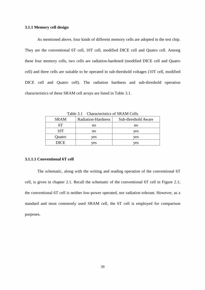
3.1.1 Memory cell design
As mentioned above, four kinds of different memory cells are adopted in the test chip.
They are the conventional 6T cell, 10T cell, modified DICE cell and Quatro cell. Among
these four memory cells, two cells are radiation-hardened (modified DICE cell and Quatro
cell) and three cells are suitable to be operated in sub-threshold voltages (10T cell, modified
DICE cell and Quatro cell). The radiation hardness and sub-threshold operation
characteristics of these SRAM cell arrays are listed in Table 3.1.
Table 3.1 Characteristics of SRAM Cells
SRAM Radiation-Hardness Sub-threshold Aware
6T no no
10T no yes
Quatro yes yes
DICE yes yes
3.1.1.1 Conventional 6T cell
The schematic, along with the writing and reading operation of the conventional 6T
cell, is given in chapter 2.1. Recall the schematic of the conventional 6T cell in Figure 2.1;
the conventional 6T cell is neither low-power operated, nor radiation tolerant. However, as a
standard and most commonly used SRAM cell, the 6T cell is employed for comparison
purposes.
40
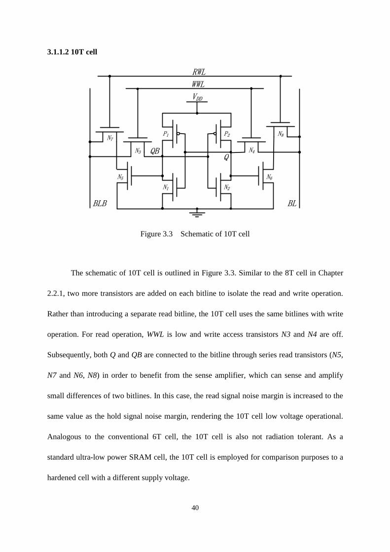
3.1.1.2 10T cell
Figure 3.3 Schematic of 10T cell
The schematic of 10T cell is outlined in Figure 3.3. Similar to the 8T cell in Chapter
2.2.1, two more transistors are added on each bitline to isolate the read and write operation.
Rather than introducing a separate read bitline, the 10T cell uses the same bitlines with write
operation. For read operation, WWL is low and write access transistors N3 and N4 are off.
Subsequently, both Q and QB are connected to the bitline through series read transistors (N5,
N7 and N6, N8) in order to benefit from the sense amplifier, which can sense and amplify
small differences of two bitlines. In this case, the read signal noise margin is increased to the
same value as the hold signal noise margin, rendering the 10T cell low voltage operational.
Analogous to the conventional 6T cell, the 10T cell is also not radiation tolerant. As a
standard ultra-low power SRAM cell, the 10T cell is employed for comparison purposes to a
hardened cell with a different supply voltage.
WWL
VDD
P1 P2
N1 N2
N3 N4Q
QB
BLB BL
RWL
N5
N7
N6
N8
41
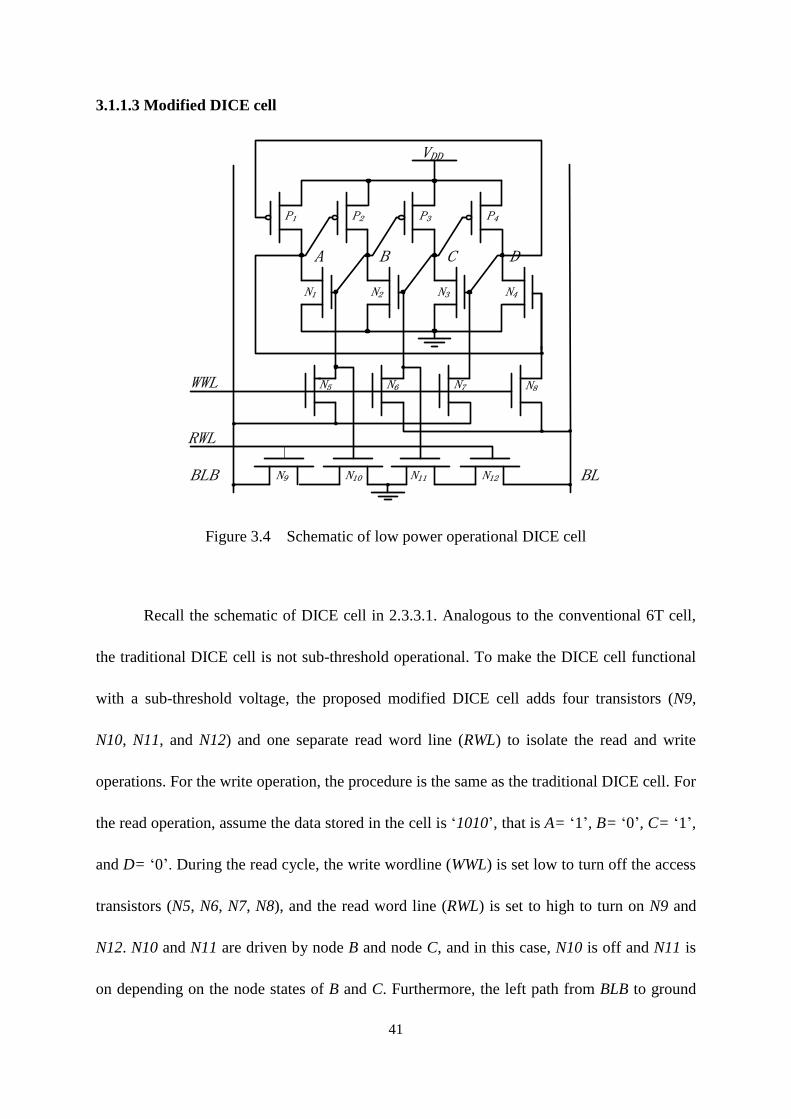
3.1.1.3 Modified DICE cell
Figure 3.4 Schematic of low power operational DICE cell
Recall the schematic of DICE cell in 2.3.3.1. Analogous to the conventional 6T cell,
the traditional DICE cell is not sub-threshold operational. To make the DICE cell functional
with a sub-threshold voltage, the proposed modified DICE cell adds four transistors (N9,
N10, N11, and N12) and one separate read word line (RWL) to isolate the read and write
operations. For the write operation, the procedure is the same as the traditional DICE cell. For
the read operation, assume the data stored in the cell is ‘1010’, that is A= ‘1’, B= ‘0’, C= ‘1’,
and D= ‘0’. During the read cycle, the write wordline (WWL) is set low to turn off the access
transistors (N5, N6, N7, N8), and the read word line (RWL) is set to high to turn on N9 and
N12. N10 and N11 are driven by node B and node C, and in this case, N10 is off and N11 is
on depending on the node states of B and C. Furthermore, the left path from BLB to ground
WWL
VDD
N1
P1
BLB BL
N2 N3 N4
RWL
P2 P3 P4
N5 N6 N7 N8
N9 N10 N11 N12
A B C D
42
through N9 and N10 is blocked by N10, and BL is pulled down due to the open path from BL
to ground through N11 and N12 at the right side. Subsequently, the potential difference
between BL and BLB will be set up. It should be noted that the precharged high voltage on BL
and BLB does not affect the state on node B or node C during the read operation, as they are
connected to the gates of access transistors. Thus, the read noise margin for the modified
DICE cell is the same as the hold noise margin, ensuring that it functions at sub-threshold
power supply voltages.
The DICE cell is tolerant to SEUs, as it can recover from any single node upset
regardless of how large the energy is. However, if more than one node is affected, the cell can
be flipped. In the less advanced technologies, the probability of two particles striking at two
different nodes in one cell at the same time is rare. However, as transistor size is continuously
scaled down, the charge generated by one strike can be spread and absorbed by more than
one node. To avoid this kind of charge spread, one can try to separate sensitive pairs far from
each other by employing a layout strategy.
43
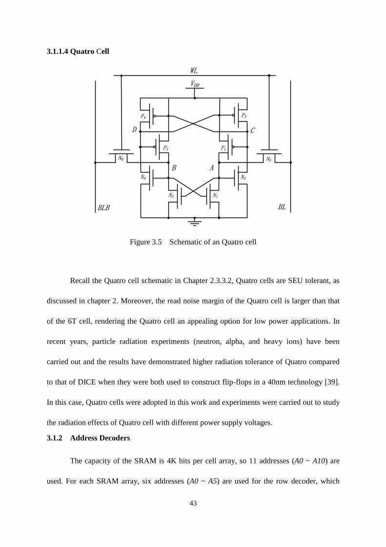
3.1.1.4 Quatro Cell
Figure 3.5 Schematic of an Quatro cell
Recall the Quatro cell schematic in Chapter 2.3.3.2, Quatro cells are SEU tolerant, as
discussed in chapter 2. Moreover, the read noise margin of the Quatro cell is larger than that
of the 6T cell, rendering the Quatro cell an appealing option for low power applications. In
recent years, particle radiation experiments (neutron, alpha, and heavy ions) have been
carried out and the results have demonstrated higher radiation tolerance of Quatro compared
to that of DICE when they were both used to construct flip-flops in a 40nm technology [39].
In this case, Quatro cells were adopted in this work and experiments were carried out to study
the radiation effects of Quatro cell with different power supply voltages.
3.1.2 Address Decoders
The capacity of the SRAM is 4K bits per cell array, so 11 addresses (A0 ~ A10) are
used. For each SRAM array, six addresses (A0 ~ A5) are used for the row decoder, which
WL
VDD
P1
P2
N1
N2
N6 N5
AB
BLB BL
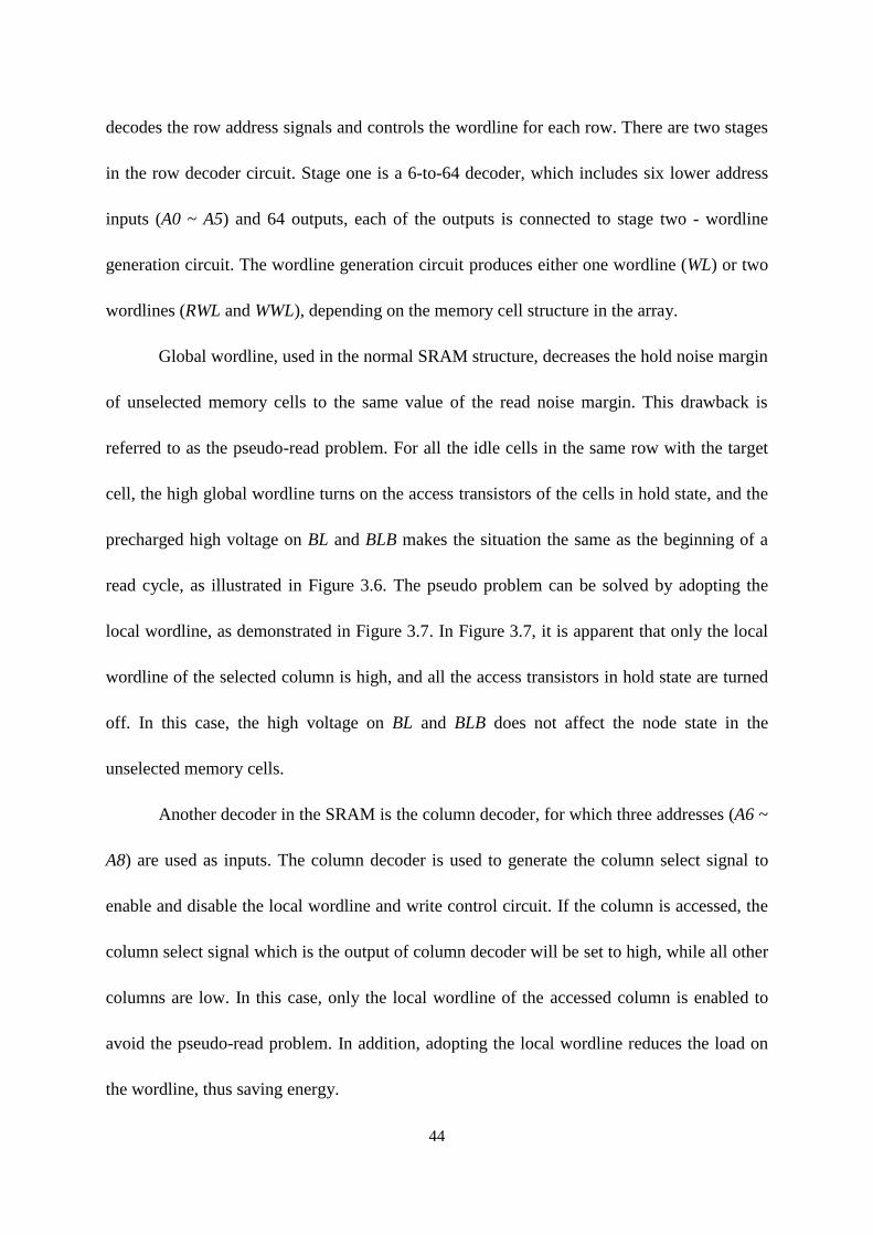
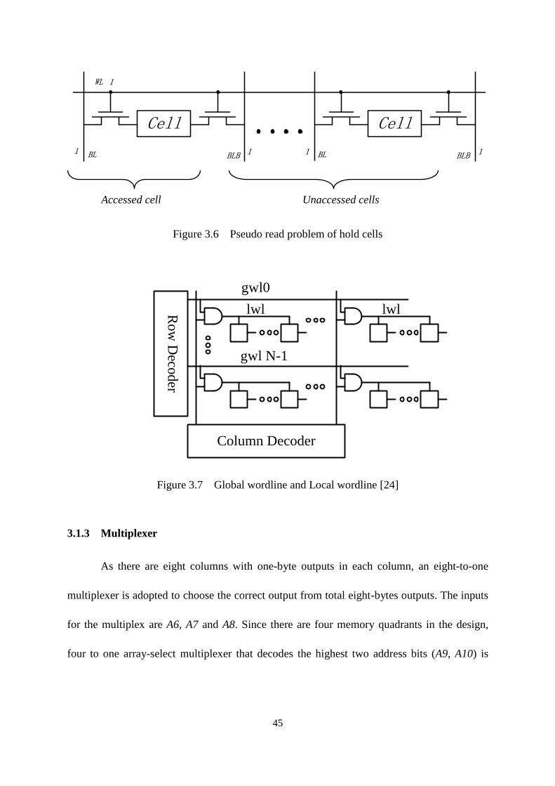
N3
N4
P3
P4
CD
44
decodes the row address signals and controls the wordline for each row. There are two stages
in the row decoder circuit. Stage one is a 6-to-64 decoder, which includes six lower address
inputs (A0 ~ A5) and 64 outputs, each of the outputs is connected to stage two - wordline
generation circuit. The wordline generation circuit produces either one wordline (WL) or two
wordlines (RWL and WWL), depending on the memory cell structure in the array.
Global wordline, used in the normal SRAM structure, decreases the hold noise margin
of unselected memory cells to the same value of the read noise margin. This drawback is
referred to as the pseudo-read problem. For all the idle cells in the same row with the target
cell, the high global wordline turns on the access transistors of the cells in hold state, and the
precharged high voltage on BL and BLB makes the situation the same as the beginning of a
read cycle, as illustrated in Figure 3.6. The pseudo problem can be solved by adopting the
local wordline, as demonstrated in Figure 3.7. In Figure 3.7, it is apparent that only the local
wordline of the selected column is high, and all the access transistors in hold state are turned
off. In this case, the high voltage on BL and BLB does not affect the node state in the
unselected memory cells.
Another decoder in the SRAM is the column decoder, for which three addresses (A6 ~
A8) are used as inputs. The column decoder is used to generate the column select signal to
enable and disable the local wordline and write control circuit. If the column is accessed, the
column select signal which is the output of column decoder will be set to high, while all other
columns are low. In this case, only the local wordline of the accessed column is enabled to
avoid the pseudo-read problem. In addition, adopting the local wordline reduces the load on
the wordline, thus saving energy.
45
Figure 3.6 Pseudo read problem of hold cells
Figure 3.7 Global wordline and Local wordline [24]
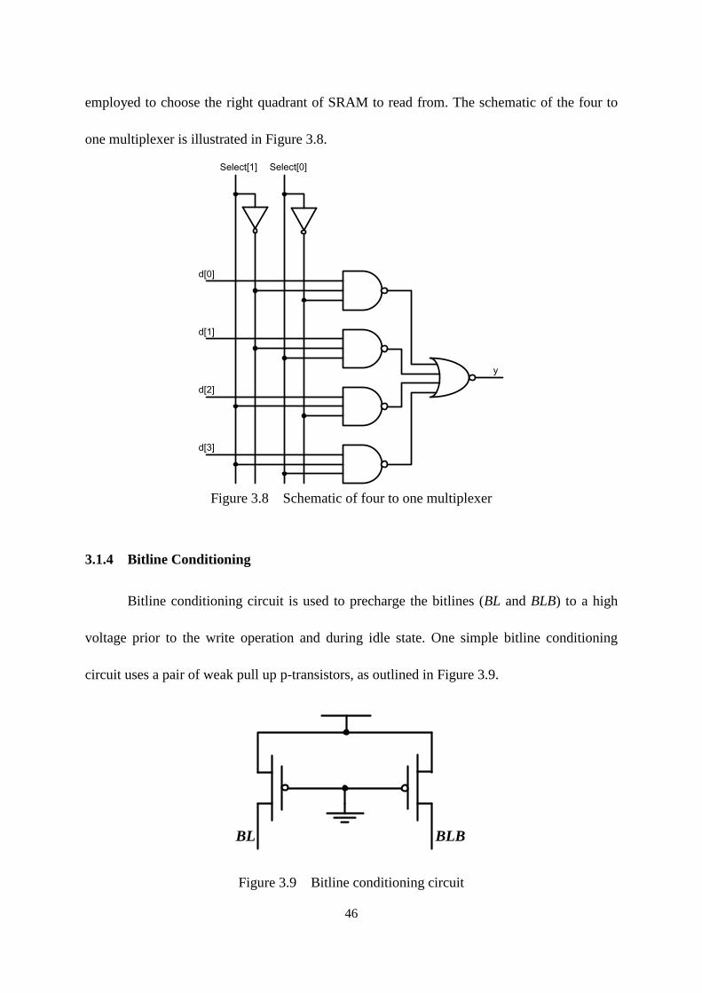
3.1.3 Multiplexer
As there are eight columns with one-byte outputs in each column, an eight-to-one
multiplexer is adopted to choose the correct output from total eight-bytes outputs. The inputs
for the multiplex are A6, A7 and A8. Since there are four memory quadrants in the design,
four to one array-select multiplexer that decodes the highest two address bits (A9, A10) is
Cell Cell
BL BLB BL BLB
WL
1 1
1
1 1
Column Decoder
Row
Deco
der
gwl0
gwl N-1
lwl lwl
Accessed cell Unaccessed cells
46
employed to choose the right quadrant of SRAM to read from. The schematic of the four to
one multiplexer is illustrated in Figure 3.8.
Select[1] Select[0]
d[0]
d[1]
d[2]
d[3]
y
Figure 3.8 Schematic of four to one multiplexer
3.1.4 Bitline Conditioning
Bitline conditioning circuit is used to precharge the bitlines (BL and BLB) to a high
voltage prior to the write operation and during idle state. One simple bitline conditioning
circuit uses a pair of weak pull up p-transistors, as outlined in Figure 3.9.
Figure 3.9 Bitline conditioning circuit
BL BLB
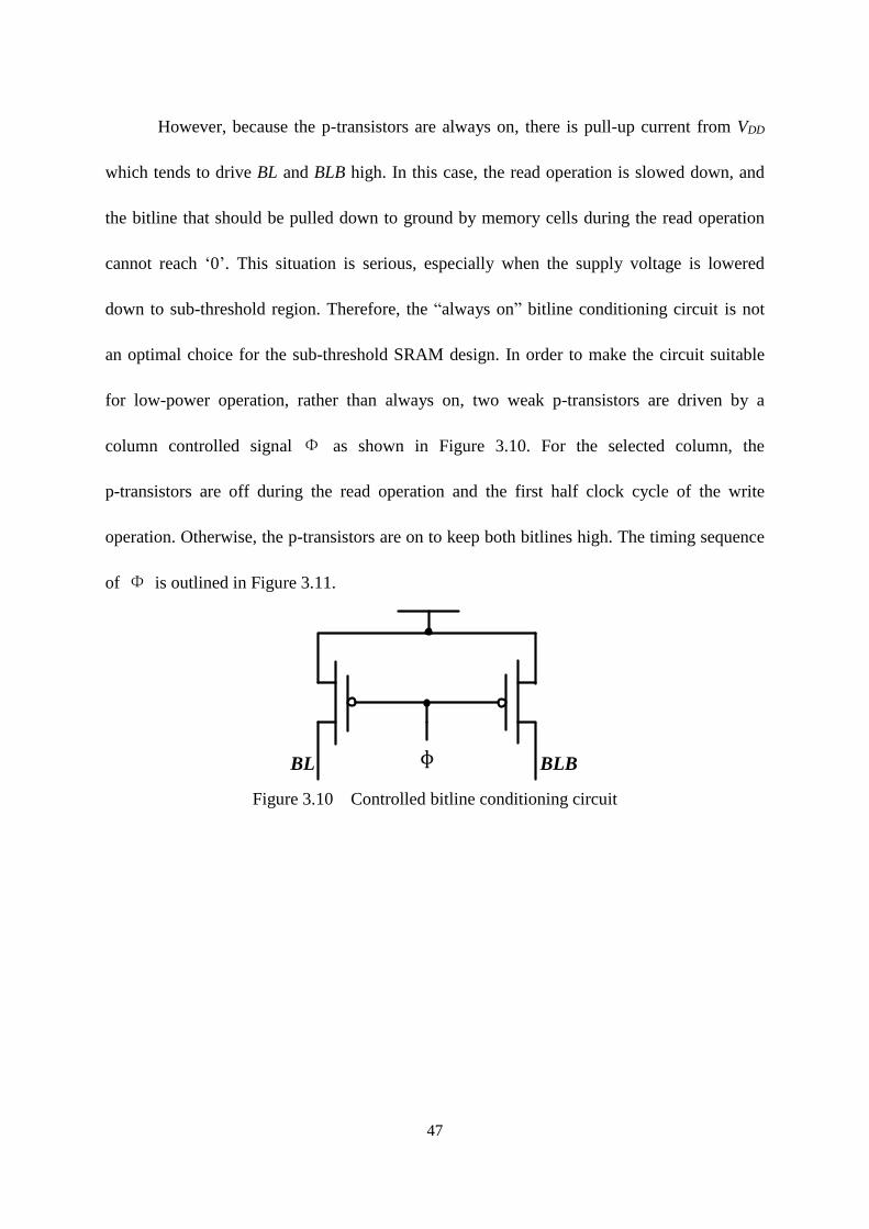
47
However, because the p-transistors are always on, there is pull-up current from VDD
which tends to drive BL and BLB high. In this case, the read operation is slowed down, and
the bitline that should be pulled down to ground by memory cells during the read operation
cannot reach ‘0’. This situation is serious, especially when the supply voltage is lowered
down to sub-threshold region. Therefore, the “always on” bitline conditioning circuit is not
an optimal choice for the sub-threshold SRAM design. In order to make the circuit suitable
for low-power operation, rather than always on, two weak p-transistors are driven by a
column controlled signal Φ as shown in Figure 3.10. For the selected column, the
p-transistors are off during the read operation and the first half clock cycle of the write
operation. Otherwise, the p-transistors are on to keep both bitlines high. The timing sequence
of Φ is outlined in Figure 3.11.
Figure 3.10 Controlled bitline conditioning circuit
BL BLBɸ
48
Figure 3.11 Timing sequence of Φ during read, write and hold operations
3.1.5 Sense Amplifier
In the SRAM design, both large-signal and small-signal sense amplifiers can be
utilized. An inverter-type read buffer can be used as a large-signal sense amplifier. However,
it requires a relatively large swing on bitline, leading to a prolonged delay and a more sizable
power consumption, as this swing must be larger than Vth. Therefore, the small-signal sense
amplifier is preferred in fast SRAM design, as only a small swing on the bitlines is required.
A dynamic latch based sense amplifier is adopted in this design, which distinguishes a small
potential difference on two bitlines and locks it to output. The bitline difference required for
this amplifier is approximately 1/10 VDD, which is much smaller than an inverter-type sense
amplifier. The schematic of the sense amplifier is illustrated in Figure 3.12.
READ HOLD/SLEEPWRITE
CLK
ɸ
RD
0V
0.3V
0V
0.3V
0V
0.3V
WR
0V
0.3V
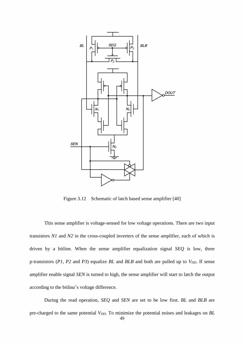
49
Figure 3.12 Schematic of latch based sense amplifier [40]
This sense amplifier is voltage-sensed for low voltage operations. There are two input
transistors N1 and N2 in the cross-coupled inverters of the sense amplifier, each of which is
driven by a bitline. When the sense amplifier equalization signal SEQ is low, three
p-transistors (P1, P2 and P3) equalize BL and BLB and both are pulled up to VDD. If sense
amplifier enable signal SEN is turned to high, the sense amplifier will start to latch the output
according to the bitline’s voltage difference.
During the read operation, SEQ and SEN are set to be low first. BL and BLB are
pre-charged to the same potential VDD. To minimize the potential noises and leakages on BL
BL BLBSEQ
SEN
DOUT
P1
P2
P3
N1 N2
N3
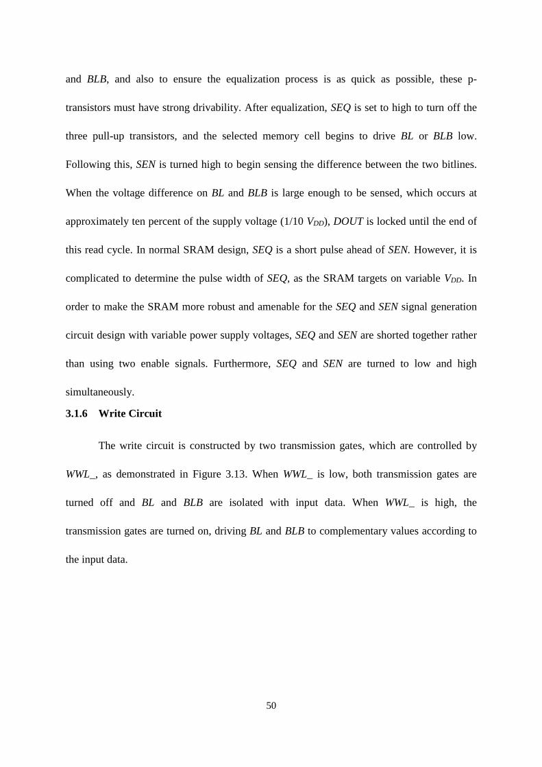
50
and BLB, and also to ensure the equalization process is as quick as possible, these p-
transistors must have strong drivability. After equalization, SEQ is set to high to turn off the
three pull-up transistors, and the selected memory cell begins to drive BL or BLB low.
Following this, SEN is turned high to begin sensing the difference between the two bitlines.
When the voltage difference on BL and BLB is large enough to be sensed, which occurs at
approximately ten percent of the supply voltage (1/10 VDD), DOUT is locked until the end of
this read cycle. In normal SRAM design, SEQ is a short pulse ahead of SEN. However, it is
complicated to determine the pulse width of SEQ, as the SRAM targets on variable VDD. In
order to make the SRAM more robust and amenable for the SEQ and SEN signal generation
circuit design with variable power supply voltages, SEQ and SEN are shorted together rather
than using two enable signals. Furthermore, SEQ and SEN are turned to low and high
simultaneously.
3.1.6 Write Circuit
The write circuit is constructed by two transmission gates, which are controlled by
WWL_, as demonstrated in Figure 3.13. When WWL_ is low, both transmission gates are
turned off and BL and BLB are isolated with input data. When WWL_ is high, the
transmission gates are turned on, driving BL and BLB to complementary values according to
the input data.
51
Figure 3.13 Schematic of the write circuit
3.1.7 Level Shifter
As the SRAM is target to be radiation tolerant with different power supply voltages,
especially for sub-threshold voltages, all inputs and outputs of the SRAM may not be the 1 V
power supply voltage. To facilitate testing, standard digital IOs provided by the component
library are required, as it is a complex task to obtain all of the inputs, which are characterized
by variable potentials and frequencies, and to efficiently and accurately monitor all of the
outputs at a high frequency. However, standard digital IOs shift 2.5 V to the standard voltage,
which is 1 V for input IOs, and shift standard voltage to 2.5 V for output IOs. In addition,
they are not compatible with the target operating supply voltage, which is 0.3 V to 1 V.
Therefore level shifters are employed to both input and output sides of the SRAM in the chip
so that the digital IOs can be used, which is set to 2.5 V for interfacing with external signals.
For the input signal, 2.5 V signals being received externally are connected to digital
input IOs, which have 2.5 V input and 1 V output to the core. To shift the 1 V signal to VDD,
WWL_
DATA_INV DATA
BLB BL
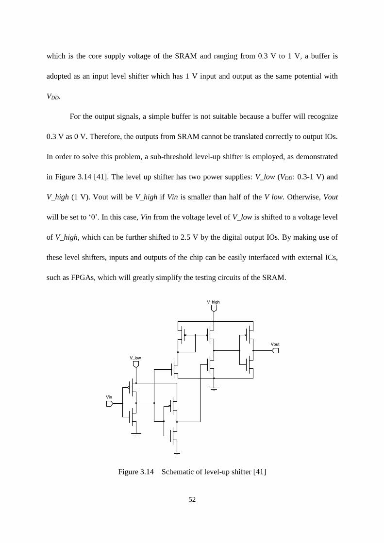
52
which is the core supply voltage of the SRAM and ranging from 0.3 V to 1 V, a buffer is
adopted as an input level shifter which has 1 V input and output as the same potential with
VDD.
For the output signals, a simple buffer is not suitable because a buffer will recognize
0.3 V as 0 V. Therefore, the outputs from SRAM cannot be translated correctly to output IOs.
In order to solve this problem, a sub-threshold level-up shifter is employed, as demonstrated
in Figure 3.14 [41]. The level up shifter has two power supplies: V_low (VDD: 0.3-1 V) and
V_high (1 V). Vout will be V_high if Vin is smaller than half of the V low. Otherwise, Vout
will be set to ‘0’. In this case, Vin from the voltage level of V_low is shifted to a voltage level
of V_high, which can be further shifted to 2.5 V by the digital output IOs. By making use of
these level shifters, inputs and outputs of the chip can be easily interfaced with external ICs,
such as FPGAs, which will greatly simplify the testing circuits of the SRAM.
Figure 3.14 Schematic of level-up shifter [41]
Vin
V_low
V_high
Vout
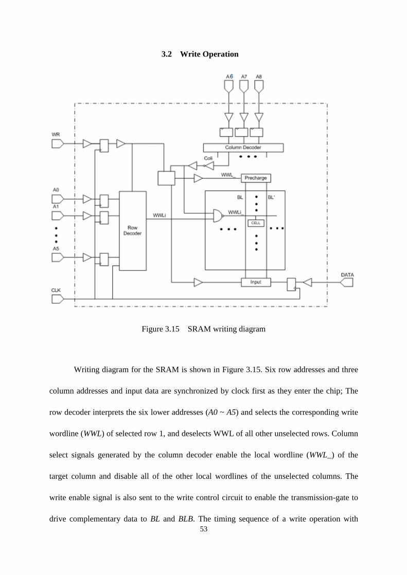
53
3.2 Write Operation
Figure 3.15 SRAM writing diagram
Writing diagram for the SRAM is shown in Figure 3.15. Six row addresses and three
column addresses and input data are synchronized by clock first as they enter the chip; The
row decoder interprets the six lower addresses (A0 ~ A5) and selects the corresponding write
wordline (WWL) of selected row 1, and deselects WWL of all other unselected rows. Column
select signals generated by the column decoder enable the local wordline (WWL_) of the
target column and disable all of the other local wordlines of the unselected columns. The
write enable signal is also sent to the write control circuit to enable the transmission-gate to
drive complementary data to BL and BLB. The timing sequence of a write operation with
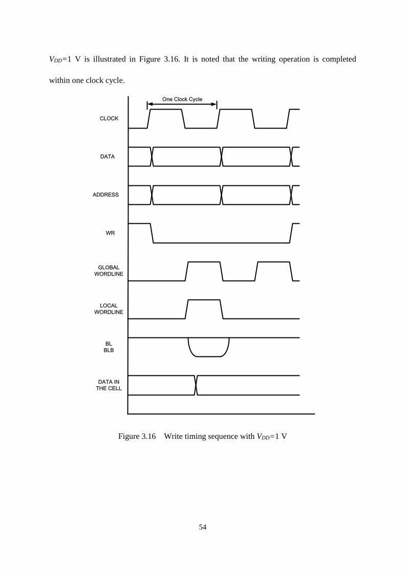
54
VDD=1 V is illustrated in Figure 3.16. It is noted that the writing operation is completed
within one clock cycle.
One Clock Cycle
CLOCK
DATA
ADDRESS
WR
GLOBAL
WORDLINE
LOCAL
WORDLINE
BL
BLB
DATA IN
THE CELL
Figure 3.16 Write timing sequence with VDD=1 V
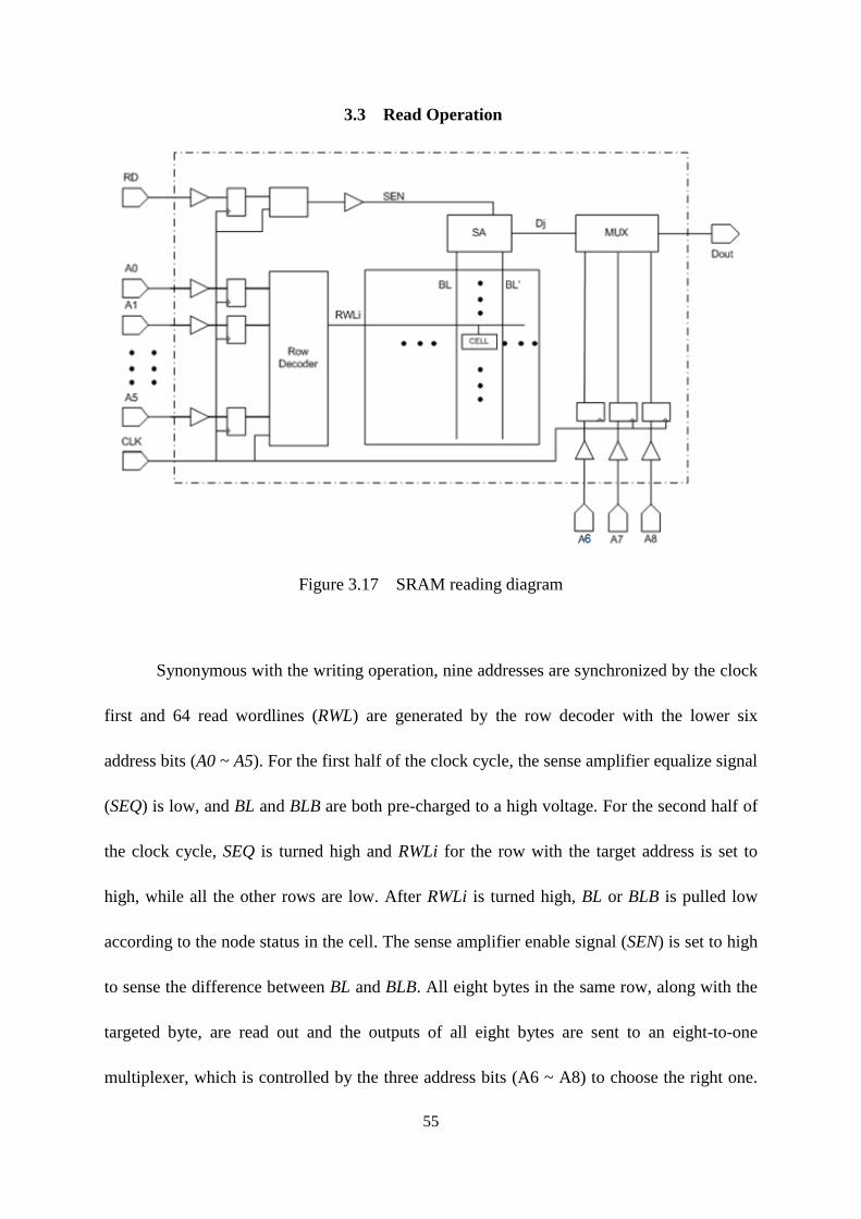
55
3.3 Read Operation
Figure 3.17 SRAM reading diagram
Synonymous with the writing operation, nine addresses are synchronized by the clock
first and 64 read wordlines (RWL) are generated by the row decoder with the lower six
address bits (A0 ~ A5). For the first half of the clock cycle, the sense amplifier equalize signal
(SEQ) is low, and BL and BLB are both pre-charged to a high voltage. For the second half of
the clock cycle, SEQ is turned high and RWLi for the row with the target address is set to
high, while all the other rows are low. After RWLi is turned high, BL or BLB is pulled low
according to the node status in the cell. The sense amplifier enable signal (SEN) is set to high
to sense the difference between BL and BLB. All eight bytes in the same row, along with the
targeted byte, are read out and the outputs of all eight bytes are sent to an eight-to-one
multiplexer, which is controlled by the three address bits (A6 ~ A8) to choose the right one.
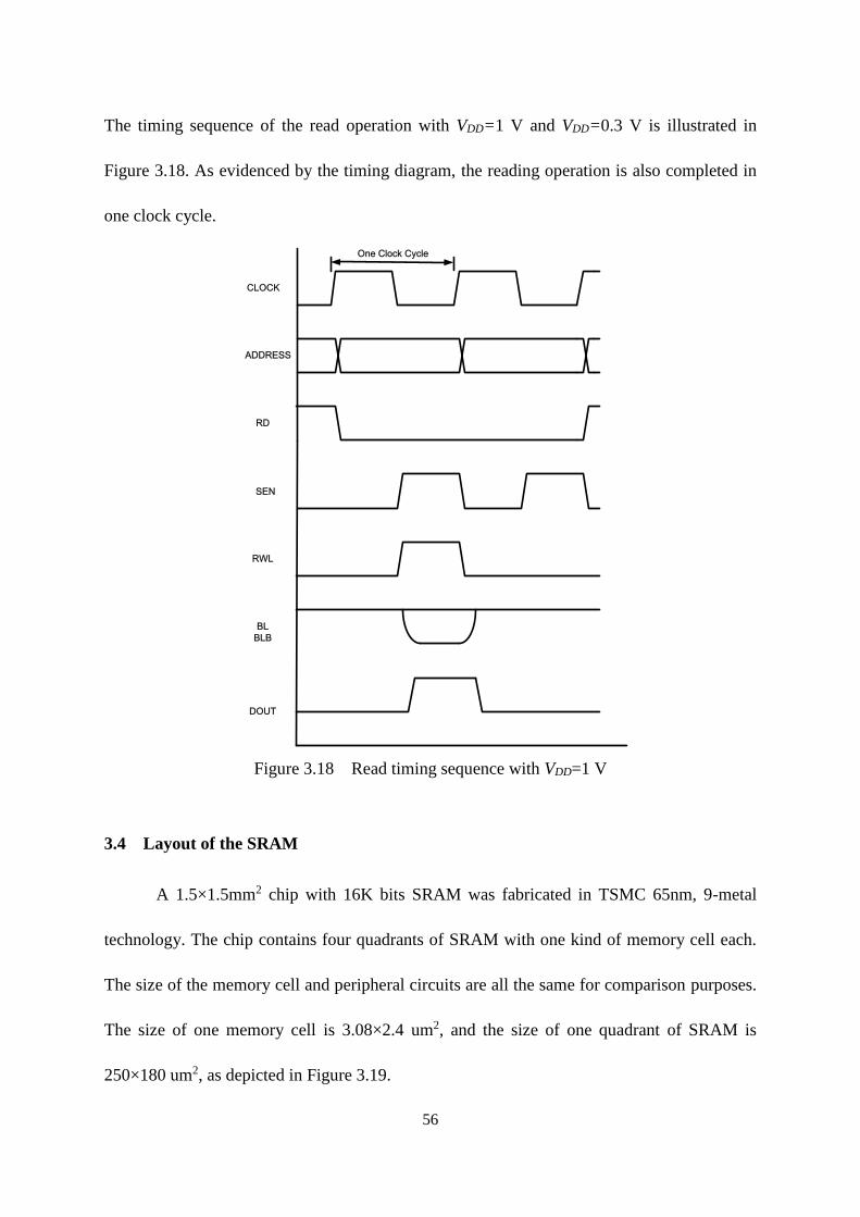
56
The timing sequence of the read operation with VDD=1 V and VDD=0.3 V is illustrated in
Figure 3.18. As evidenced by the timing diagram, the reading operation is also completed in
one clock cycle.
One Clock Cycle
CLOCK
ADDRESS
RD
SEN
RWL
BL
BLB
DOUT
Figure 3.18 Read timing sequence with VDD=1 V
3.4 Layout of the SRAM
A 1.5×1.5mm2 chip with 16K bits SRAM was fabricated in TSMC 65nm, 9-metal
technology. The chip contains four quadrants of SRAM with one kind of memory cell each.
The size of the memory cell and peripheral circuits are all the same for comparison purposes.
The size of one memory cell is 3.08×2.4 um2, and the size of one quadrant of SRAM is
250×180 um2, as depicted in Figure 3.19.

57
Figure 3.19 Layout of one quadrant of the SRAM design
Several small regions inside of the SRAM layout are not covered by dummy filling
metals; these areas can be tested by the pulse laser facility in Saskatchewan Structural
Decoder 4k-bit memory cell array
Write Circuit and SA Multiplexer
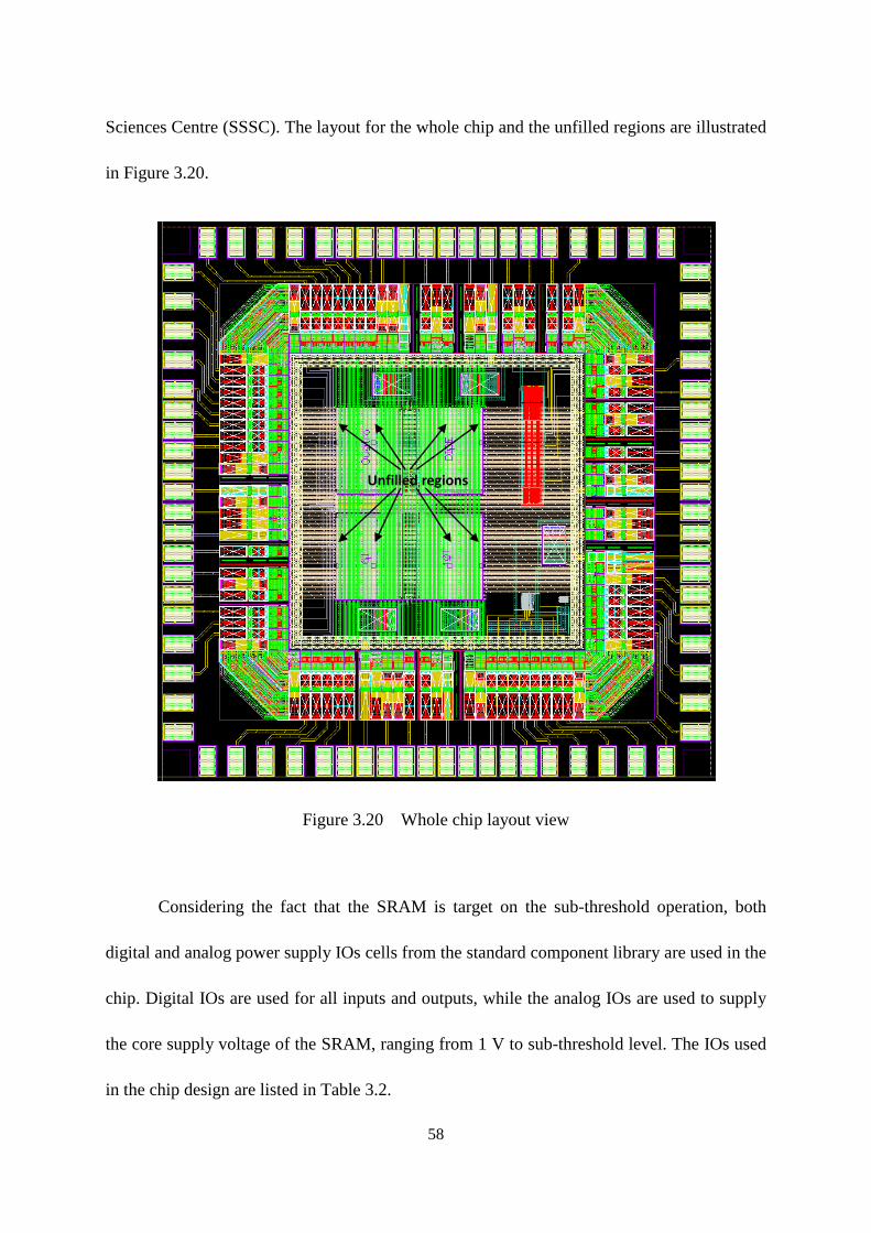
58
Sciences Centre (SSSC). The layout for the whole chip and the unfilled regions are illustrated
in Figure 3.20.
Figure 3.20 Whole chip layout view
Considering the fact that the SRAM is target on the sub-threshold operation, both
digital and analog power supply IOs cells from the standard component library are used in the
chip. Digital IOs are used for all inputs and outputs, while the analog IOs are used to supply
the core supply voltage of the SRAM, ranging from 1 V to sub-threshold level. The IOs used
in the chip design are listed in Table 3.2.
Unfilled regions
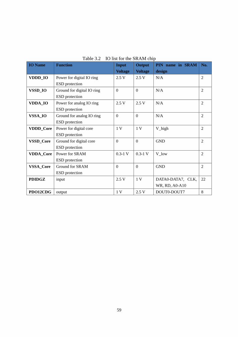
59
Table 3.2 IO list for the SRAM chip
IO Name Function Input
Voltage
Output
Voltage
PIN name in SRAM
design
No.
VDDD_IO Power for digital IO ring
ESD protection
2.5 V 2.5 V N/A 2
VSSD_IO Ground for digital IO ring
ESD protection
0 0 N/A 2
VDDA_IO Power for analog IO ring
ESD protection
2.5 V 2.5 V N/A 2
VSSA_IO Ground for analog IO ring
ESD protection
0 0 N/A 2
VDDD_Core Power for digital core
ESD protection
1 V 1 V V_high 2
VSSD_Core Ground for digital core
ESD protection
0 0 GND 2
VDDA_Core Power for SRAM
ESD protection
0.3-1 V 0.3-1 V V_low 2
VSSA_Core Ground for SRAM
ESD protection
0 0 GND 2
PDIDGZ input 2.5 V 1 V DATA0-DATA7, CLK,
WR, RD, A0-A10
22
PDO12CDG output 1 V 2.5 V DOUT0-DOUT7 8
60
CHAPTER 4
SIMULATION RESULTs
4.1 Memory cell simulation
4.1.1 Signal Noise Margin
In order to achieve the objective of operating in sub-threshold voltage range, signal
noise margin discussed in Chapter 2 must be taken into account, as it is one of the most
important criterions for ultra low-power SRAM design. Signal noise margin can be acquired
by voltage transfer characteristic (VTC).
The configuration for SNM simulation is the same as what was depicted in Figure 2.6
and Figure 2.7. In regards to the read noise margin, BL, BLB and WL are all set to be high.
For the hold noise margin, BL and BLB are also set to high and WL is biased to GND. The
read and hold noise margins can be extracted by VTC curve, which is acquired by sweeping
one node of memory cell (Q or QB) from 0 to VDD and monitoring the potential on the other
node (QB or Q). Butterfly curves for RSNM, as shown in Figure 4.1, for all four cells are
obtained by plotting Q versus QB and, subsequently, plotting QB versus Q. SNM is
determined by the size of the maximum square in the butterfly curve. All VTC curves of four
SRAM cell are simulated with VDD changes from 0.3 V to 1 V by 0.1 V step. HSNM and
RSNM of the four cells are depicted in Figure 4.2.
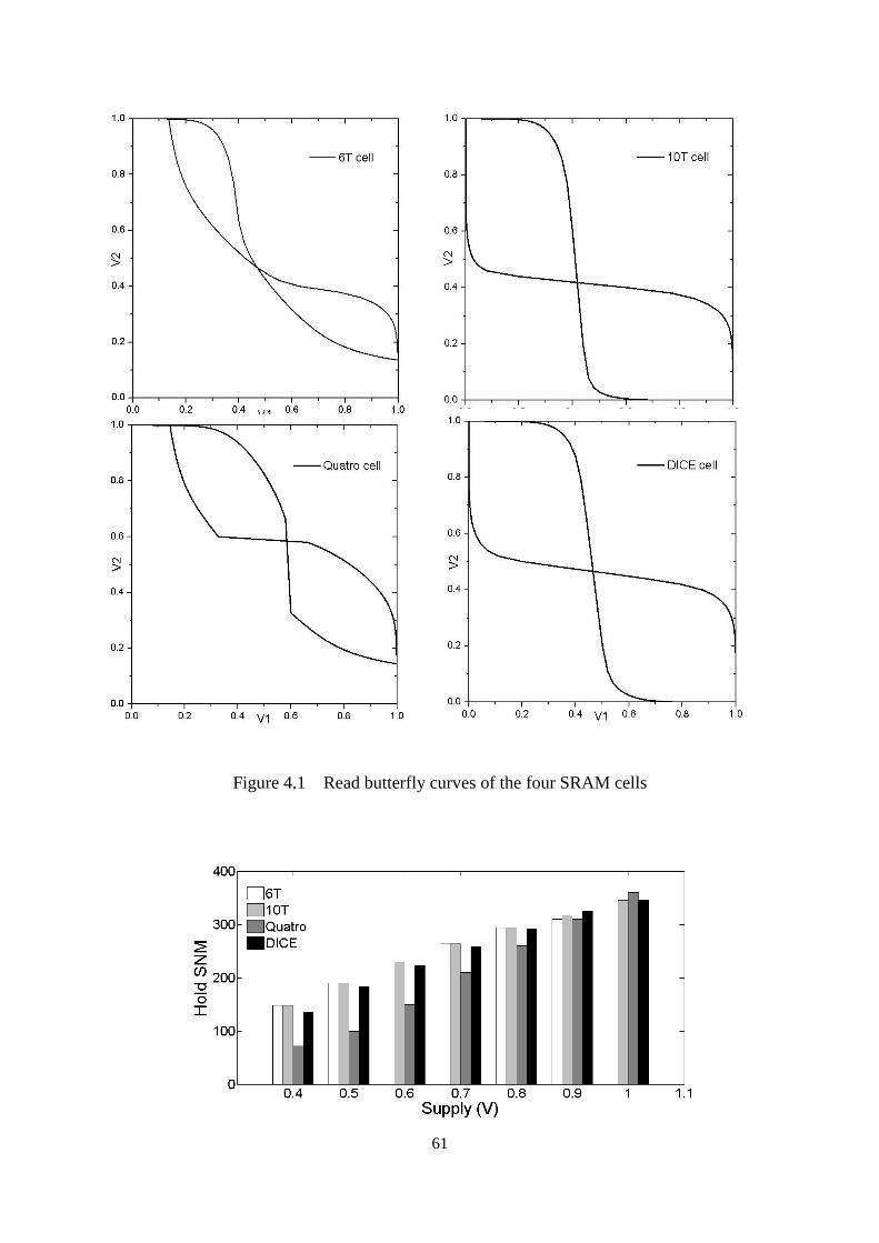
61
Figure 4.1 Read butterfly curves of the four SRAM cells
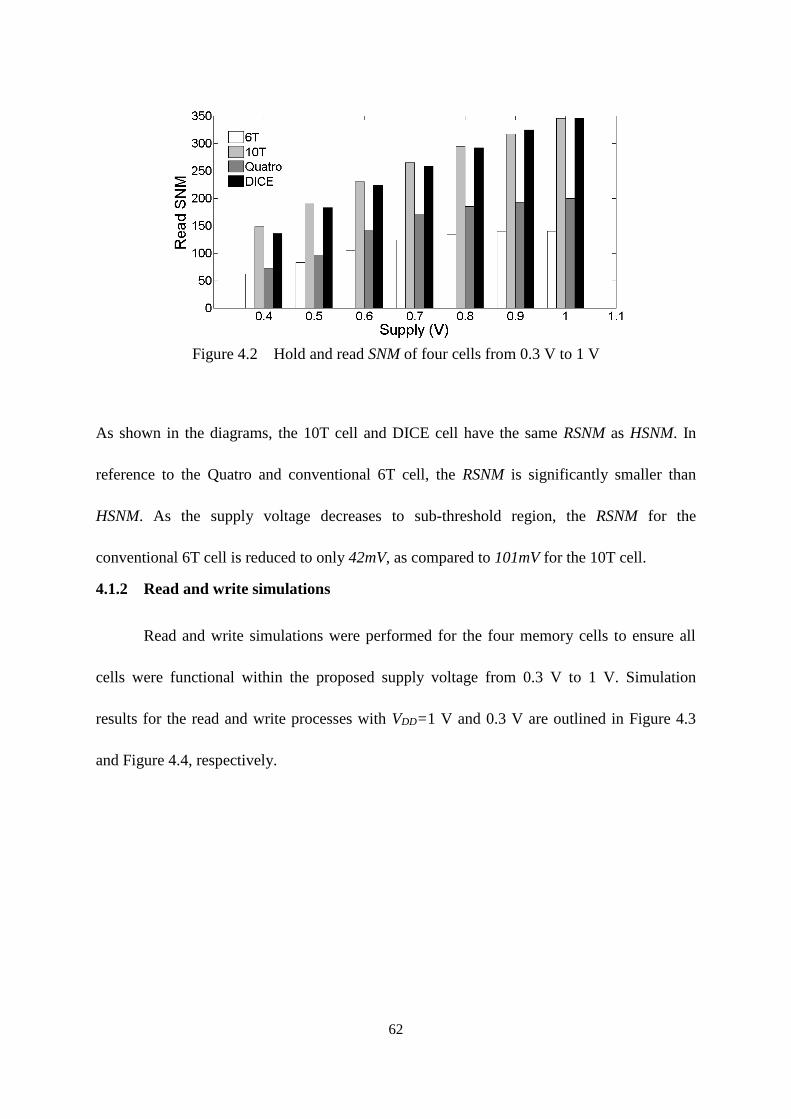
62
Figure 4.2 Hold and read SNM of four cells from 0.3 V to 1 V
As shown in the diagrams, the 10T cell and DICE cell have the same RSNM as HSNM. In
reference to the Quatro and conventional 6T cell, the RSNM is significantly smaller than
HSNM. As the supply voltage decreases to sub-threshold region, the RSNM for the
conventional 6T cell is reduced to only 42mV, as compared to 101mV for the 10T cell.
4.1.2 Read and write simulations
Read and write simulations were performed for the four memory cells to ensure all
cells were functional within the proposed supply voltage from 0.3 V to 1 V. Simulation
results for the read and write processes with VDD=1 V and 0.3 V are outlined in Figure 4.3
and Figure 4.4, respectively.
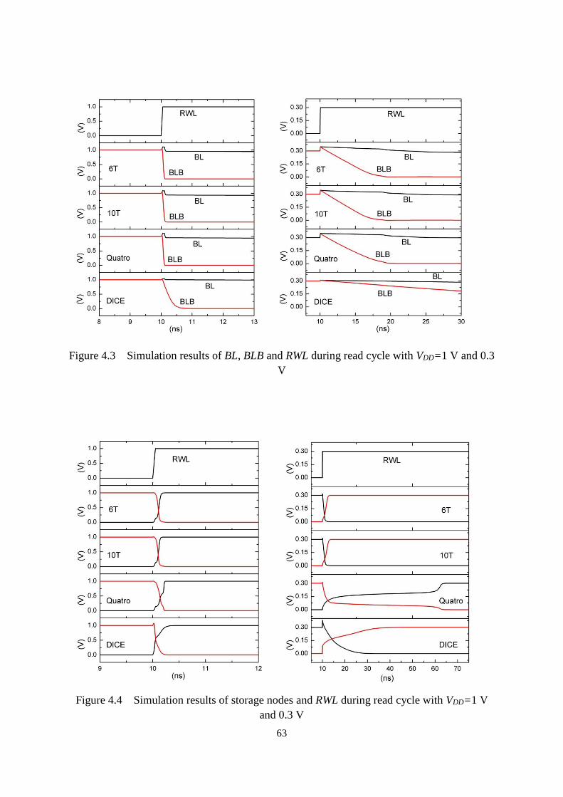
63
Figure 4.3 Simulation results of BL, BLB and RWL during read cycle with VDD=1 V and 0.3
V
Figure 4.4 Simulation results of storage nodes and RWL during read cycle with VDD=1 V
and 0.3 V
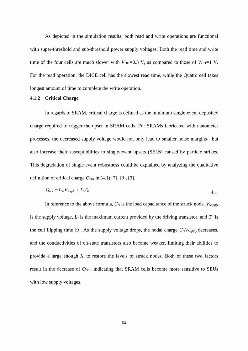
64
As depicted in the simulation results, both read and write operations are functional
with super-threshold and sub-threshold power supply voltages. Both the read time and write
time of the four cells are much slower with VDD=0.3 V, as compared to those of VDD=1 V.
For the read operation, the DICE cell has the slowest read time, while the Quatro cell takes
longest amount of time to complete the write operation.
4.1.2 Critical Charge
In regards to SRAM, critical charge is defined as the minimum single-event deposited
charge required to trigger the upset in SRAM cells. For SRAMs fabricated with nanometer
processes, the decreased supply voltage would not only lead to smaller noise margins,but
also increase their susceptibilities to single-event upsets (SEUs) caused by particle strikes.
This degradation of single-event robustness could be explained by analyzing the qualitative
definition of critical charge Qcrit in (4.1) [7], [8], [9].
4.1
In reference to the above formula, CN is the load capacitance of the struck node, VSupply
is the supply voltage, ID is the maximum current provided by the driving transistor, and TF is
the cell flipping time [9]. As the supply voltage drops, the nodal charge CNVSupply decreases,
and the conductivities of on-state transistors also become weaker, limiting their abilities to
provide a large enough ID to restore the levels of struck nodes. Both of these two factors
result in the decrease of Qcrit, indicating that SRAM cells become more sensitive to SEUs
with low supply voltages.
crit N Supply D FQ C V I T
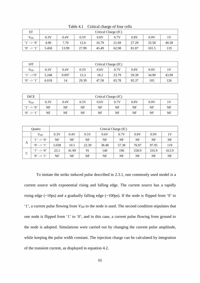
65
Table 4.1 Critical charge of four cells
6T Critical Charge (fC)
VDD 0.3V 0.4V 0.5V 0.6V 0.7V 0.8V 0.9V 1V
‘1’ –> ‘0’ 4.90 7.70 12.6 16.79 21.69 27.29 33.58 40.58
‘0’ –> ‘1’ 5.458 13.99 27.99 45.49 62.98 81.87 101.5 119
10T Critical Charge (fC)
VDD 0.3V 0.4V 0.5V 0.6V 0.7V 0.8V 0.9V 1V
‘1’ –>‘0’ 5.248 9.097 13.3 18.2 23.79 29.39 34.99 43.99
‘0’ –> ‘1’ 6.018 14 29.39 47.58 65.78 85.37 105 126
DICE Critical Charge (fC)
VDD 0.3V 0.4V 0.5V 0.6V 0.7V 0.8V 0.9V 1V
‘1’ –> ‘0’ NF NF NF NF NF NF NF NF
‘0’ –> ‘1’ NF NF NF NF NF NF NF NF
Quatro Critical Charge (fC)
VDD 0.3V 0.4V 0.5V 0.6V 0.7V 0.8V 0.9V 1V
A ‘1’ –> ‘0’ NF NF NF NF NF NF NF NF
‘0’ –> ‘1’ 5.038 10.5 22.39 38.48 57.38 76.97 97.95 119
C ‘1’ –> ‘0’ 23.1 41.99 91 140 196 258.9 335.9 412.9
‘0’ –> ‘1’ NF NF NF NF NF NF NF NF
To imitate the strike induced pulse described in 2.3.1, one commonly used model is a
current source with exponential rising and falling edge. The current source has a rapidly
rising edge (~10ps) and a gradually falling edge (~100ps). If the node is flipped from ‘0’ to
‘1’, a current pulse flowing from VDD to the node is used. The second condition stipulates that
one node is flipped from ‘1’ to ‘0’, and in this case, a current pulse flowing from ground to
the node is adopted. Simulations were carried out by changing the current pulse amplitude,
while keeping the pulse width constant. The injection charge can be calculated by integration
of the transient current, as displayed in equation 4.2.
66
4.2
The simulation results for the critical charge of four cells are listed in Table 4.1. In the
table, NF signifies that no flip occurs.
Conclusions can be drawn from the above simulation results.
1. The conventional 6T cell has the lowest critical charge, while the 10T cell has a slightly
higher critical charge than the 6T cell, and both cells can be easily flipped by radiation
when the supply voltage ranges from 0.3 V to 1 V.
2. SEU cannot be triggered to the DICE cell if only the single node is affected, regardless of
how large the injected current is.
3. The Quatro cell can be upset in two cases: one is to flip ‘0’ to ‘1’ at node A, and the other
one is to flip ‘1’ to ‘0’ at node C. However, the critical charge required for these kinds of
flips is much larger than that of the conventional 6T cell; the charge is ~3 times for node
A and ~10 times for node C. In regards to other conditions, Quatro cells are SEU tolerant.
4. For conventional 6T cells, the critical charge required to flip the node from ‘0’ to ‘1’ is
about 3 times higher than the charge needed to flip the node from ‘1’ to ‘0’. As discussed
in 2.3.2, the most sensitive node for SEU is the reverse-biased transistors in the substrate.
Recall the schematic of conventional 6T cell in Figure 2.1; assuming that the initial state
is Q=‘1’, if Q is flipped from ‘1’ to ‘0’, the transistor which is struck by the particle is N2.
If QB is upset from ‘0’ to ‘1’, the transistor got struke by the particle is P1. Both P1 and
N2 are reverse-biased transistors. As P1 lies in a well while N2 is located in the substrate,
less energy is required to flip N2 than P1, according to the theory outlined in 2.3.2.
0( )
tf
crit injt
Q I t dt
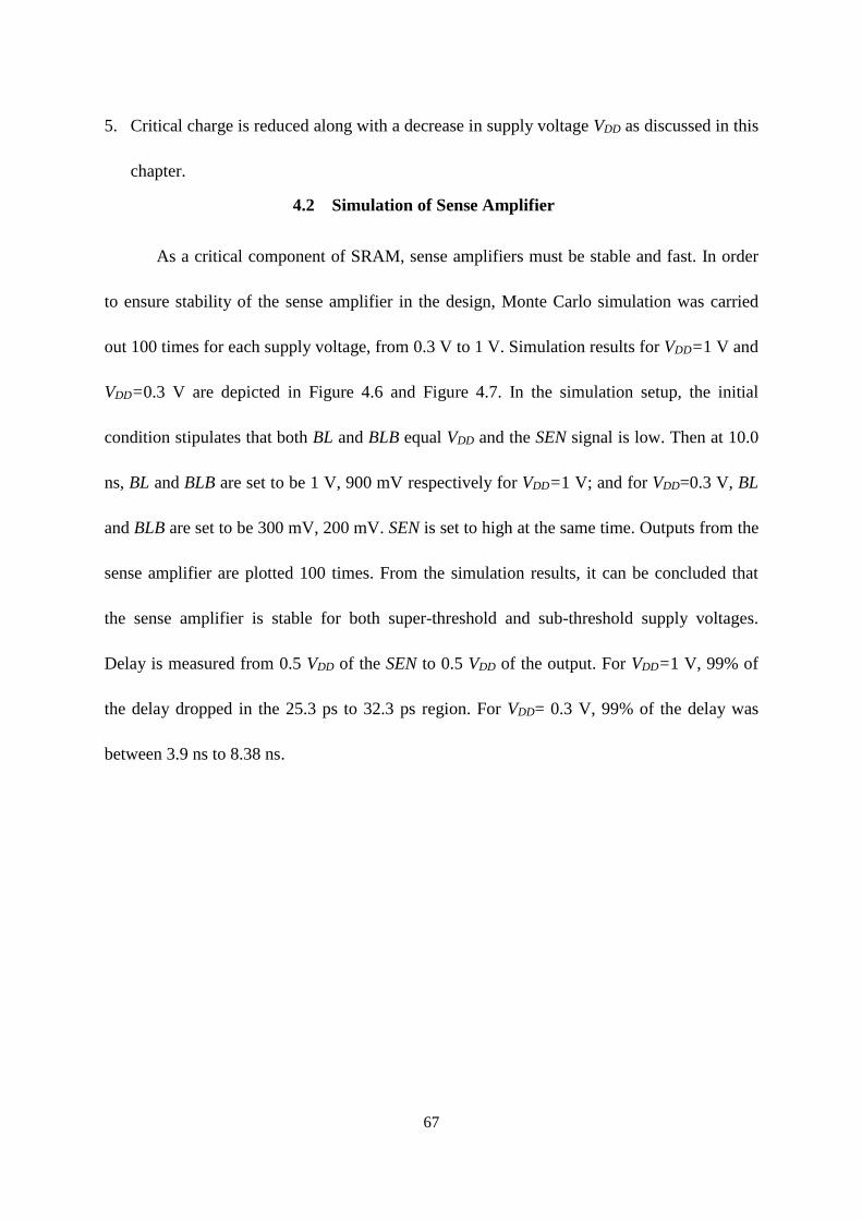
67
5. Critical charge is reduced along with a decrease in supply voltage VDD as discussed in this
chapter.
4.2 Simulation of Sense Amplifier
As a critical component of SRAM, sense amplifiers must be stable and fast. In order
to ensure stability of the sense amplifier in the design, Monte Carlo simulation was carried
out 100 times for each supply voltage, from 0.3 V to 1 V. Simulation results for VDD=1 V and
VDD=0.3 V are depicted in Figure 4.6 and Figure 4.7. In the simulation setup, the initial
condition stipulates that both BL and BLB equal VDD and the SEN signal is low. Then at 10.0
ns, BL and BLB are set to be 1 V, 900 mV respectively for VDD=1 V; and for VDD=0.3 V, BL
and BLB are set to be 300 mV, 200 mV. SEN is set to high at the same time. Outputs from the
sense amplifier are plotted 100 times. From the simulation results, it can be concluded that
the sense amplifier is stable for both super-threshold and sub-threshold supply voltages.
Delay is measured from 0.5 VDD of the SEN to 0.5 VDD of the output. For VDD=1 V, 99% of
the delay dropped in the 25.3 ps to 32.3 ps region. For VDD= 0.3 V, 99% of the delay was
between 3.9 ns to 8.38 ns.
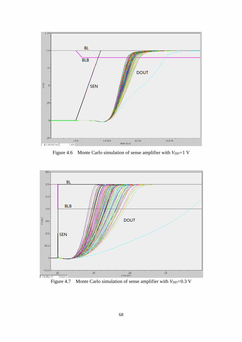
68
Figure 4.6 Monte Carlo simulation of sense amplifier with VDD=1 V
Figure 4.7 Monte Carlo simulation of sense amplifier with VDD=0.3 V
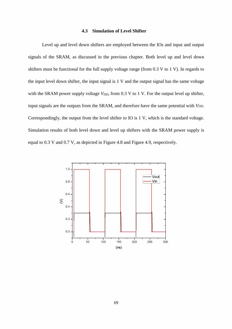
69
4.3 Simulation of Level Shifter
Level up and level down shifters are employed between the IOs and input and output
signals of the SRAM, as discussed in the previous chapter. Both level up and level down
shifters must be functional for the full supply voltage range (from 0.3 V to 1 V). In regards to
the input level down shifter, the input signal is 1 V and the output signal has the same voltage
with the SRAM power supply voltage VDD, from 0.3 V to 1 V. For the output level up shifter,
input signals are the outputs from the SRAM, and therefore have the same potential with VDD.
Correspondingly, the output from the level shifter to IO is 1 V, which is the standard voltage.
Simulation results of both level down and level up shifters with the SRAM power supply is
equal to 0.3 V and 0.7 V, as depicted in Figure 4.8 and Figure 4.9, respectively.
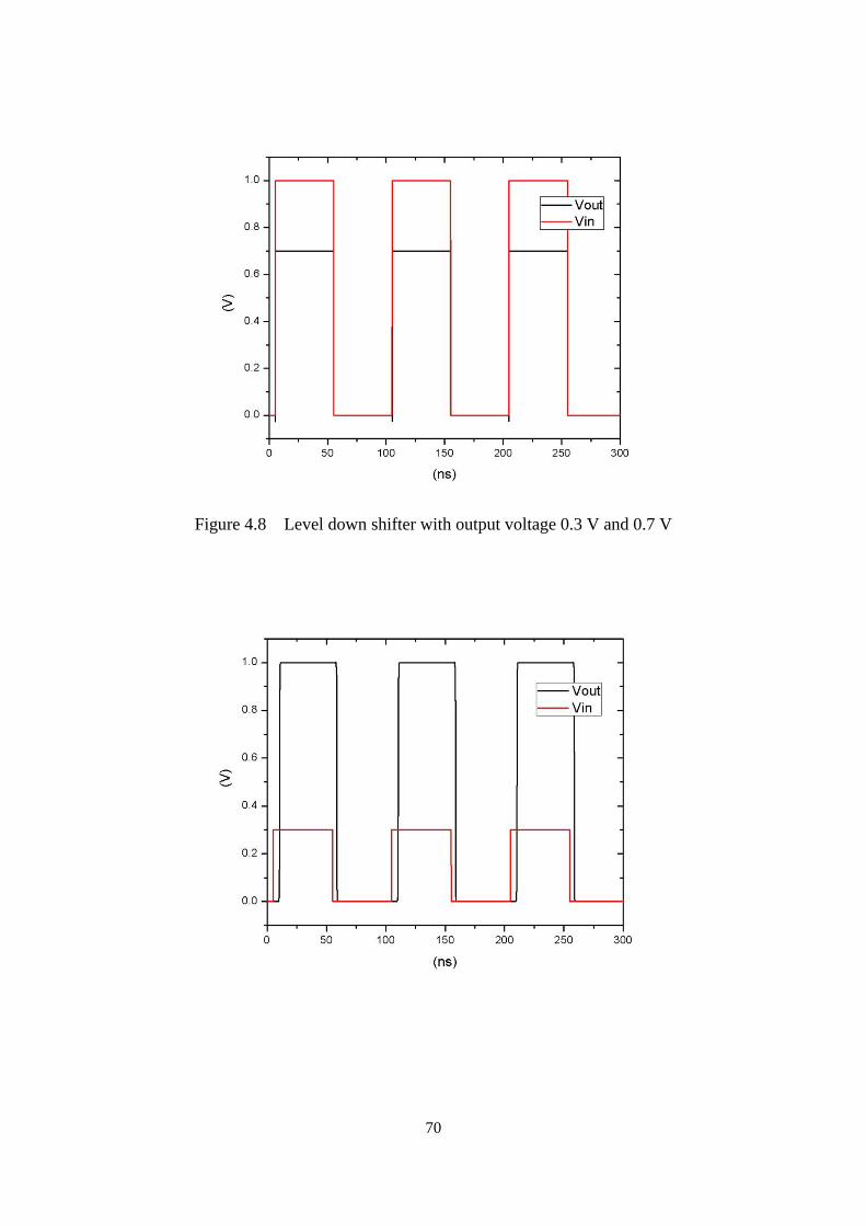
70
Figure 4.8 Level down shifter with output voltage 0.3 V and 0.7 V
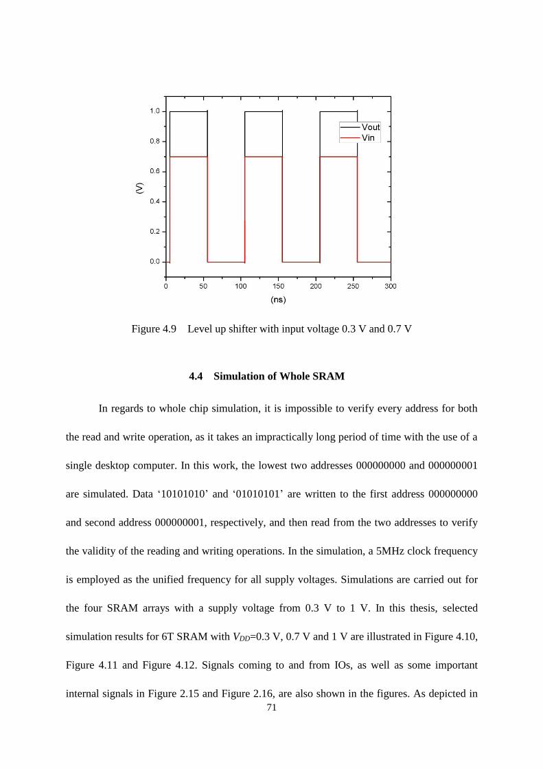
71
Figure 4.9 Level up shifter with input voltage 0.3 V and 0.7 V
4.4 Simulation of Whole SRAM
In regards to whole chip simulation, it is impossible to verify every address for both
the read and write operation, as it takes an impractically long period of time with the use of a
single desktop computer. In this work, the lowest two addresses 000000000 and 000000001
are simulated. Data ‘10101010’ and ‘01010101’ are written to the first address 000000000
and second address 000000001, respectively, and then read from the two addresses to verify
the validity of the reading and writing operations. In the simulation, a 5MHz clock frequency
is employed as the unified frequency for all supply voltages. Simulations are carried out for
the four SRAM arrays with a supply voltage from 0.3 V to 1 V. In this thesis, selected
simulation results for 6T SRAM with VDD=0.3 V, 0.7 V and 1 V are illustrated in Figure 4.10,
Figure 4.11 and Figure 4.12. Signals coming to and from IOs, as well as some important
internal signals in Figure 2.15 and Figure 2.16, are also shown in the figures. As depicted in
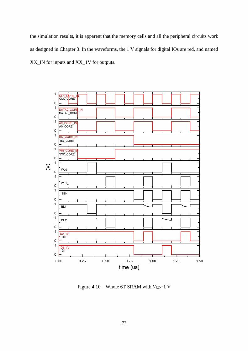
72
the simulation results, it is apparent that the memory cells and all the peripheral circuits work
as designed in Chapter 3. In the waveforms, the 1 V signals for digital IOs are red, and named
XX_IN for inputs and XX_1V for outputs.
Figure 4.10 Whole 6T SRAM with VDD=1 V
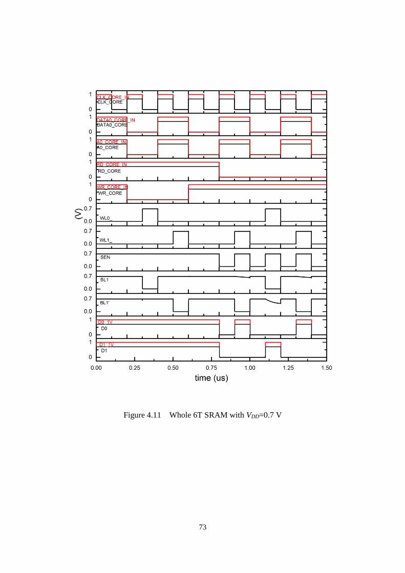
73
Figure 4.11 Whole 6T SRAM with VDD=0.7 V

74
Figure 4.10 Whole 6T SRAM with VDD=0.3 V
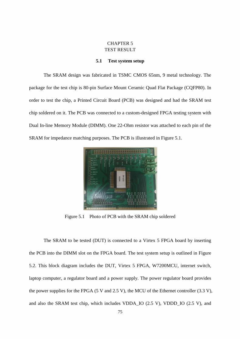
75
CHAPTER 5
TEST RESULT
5.1 Test system setup
The SRAM design was fabricated in TSMC CMOS 65nm, 9 metal technology. The
package for the test chip is 80-pin Surface Mount Ceramic Quad Flat Package (CQFP80). In
order to test the chip, a Printed Circuit Board (PCB) was designed and had the SRAM test
chip soldered on it. The PCB was connected to a custom-designed FPGA testing system with
Dual In-line Memory Module (DIMM). One 22-Ohm resistor was attached to each pin of the
SRAM for impedance matching purposes. The PCB is illustrated in Figure 5.1.
Figure 5.1 Photo of PCB with the SRAM chip soldered
The SRAM to be tested (DUT) is connected to a Virtex 5 FPGA board by inserting
the PCB into the DIMM slot on the FPGA board. The test system setup is outlined in Figure
5.2. This block diagram includes the DUT, Virtex 5 FPGA, W7200MCU, internet switch,
laptop computer, a regulator board and a power supply. The power regulator board provides
the power supplies for the FPGA (5 V and 2.5 V), the MCU of the Ethernet controller (3.3 V),
and also the SRAM test chip, which includes VDDA_IO (2.5 V), VDDD_IO (2.5 V), and
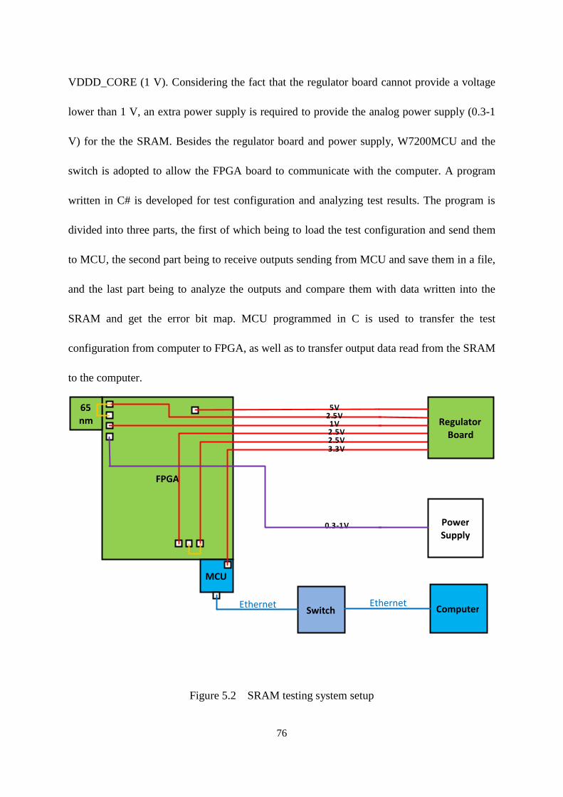
76
VDDD_CORE (1 V). Considering the fact that the regulator board cannot provide a voltage
lower than 1 V, an extra power supply is required to provide the analog power supply (0.3-1
V) for the the SRAM. Besides the regulator board and power supply, W7200MCU and the
switch is adopted to allow the FPGA board to communicate with the computer. A program
written in C# is developed for test configuration and analyzing test results. The program is
divided into three parts, the first of which being to load the test configuration and send them
to MCU, the second part being to receive outputs sending from MCU and save them in a file,
and the last part being to analyze the outputs and compare them with data written into the
SRAM and get the error bit map. MCU programmed in C is used to transfer the test
configuration from computer to FPGA, as well as to transfer output data read from the SRAM
to the computer.
Figure 5.2 SRAM testing system setup
FPGA
MCU
65
nm
5 V 2 . 5 V 1 V
0 . 3 - 1 V
2 . 5 V 2 . 5 V
Regulator
Board
Power
Supply
Switch Computer
3 . 3 V
Ethernet Ethernet
77
At the beginning of the testing, data pattern, clock frequency, and SRAM array are
selected by the configuration data file and loaded into the PC program. Following this, the
configuration data is sent to the W7200MCU and then transferred to the PFGA. The FPGA
generates the required Clock, write enable, read enable, address and data according to the
configuration file, and is subsequently sent to the DUT. In addition, the FPGA samples
outputs from the DUT at positive clock edge and sends the results back to the MCU. After the
MCU receives all of the outputs from the targeted address, they are sent back to the computer
through the ethernet cable. All of the inputs to the DUT, with the exception of supply power,
are all 2.5 and all generated from the FPGA. The power supply to the SRAM is from the
external power supply, ranging from 0.3 V to 1 V.
5.2 Functional Test
In regards to a functional test with a variable supply voltage, the read and write
functionality test with standard voltage 1 V was performed first, ensuring that the SRAM
would perform adequately with the standard 1 V. For the read and write test with a lower
voltage than 1 V, if same voltage was used for the read and write operation, it would be hard
to determine whether it was a read error or write error. In this research, for the write test, the
data was written to the SRAM at different voltages (0.3-1 V) and then read back at a high
voltage (1 V) to ensure that the outputs were the same with the data stored in the memory
cells. For the read test, data was written to the SRAM at a high voltage (1 V) to ensure the
write data was written into the cells correctly, and subsequently read back at different
voltages. In this case, when an error occurs, it is easy to identify whether it is a read or write
error.
78
Four different data patterns are written into the SRAM and then read back from the
SRAM to investigate whether the contents are the same as what was written into the SRAM.
The four data patterns are ‘00000000’, ‘01010101’, ‘10101010’, and ‘11111111’,
respectively. These four data patterns are chosen as typical data patterns to test both ‘0’ and
‘1’ of each cell. The write and read procedure for one memory array is described in the
following steps: First, set the supply power to I V and write the same data into the SRAM
from lowest address (0) to highest address (511). Following this, read the contents out from
address 0 to 511. The testing results convey that with VDD=1 V, correct outputs can be
obtained from all addresses for all four data patterns. Furthermore, it can be concluded that
both read and write operations function as expected with the standard 1 V power supply.
After verifying the read and write functions with standard VDD, read and write testing
with lower supply voltages were performed. For the read testing, data was written into the
SRAM with VDD=1 V first to ensure that all cells were written correctly. Following this, the
supply voltage was changed to the target value and read from addresses from 0 to 511. For
the write testing, data was written into the SRAM with targeted VDD, and read from the
SRAM with the standard power supply to ensure that all outputs read from the SRAM were
synonymous with the data stored in the memory cells. All outputs were recorded and
compared to the written data.
For the write functionality testing, the results showed that all addresses were written
with correct data, with a power supply ranging from 1 V to 0.3 V. This signifies that the
SRAM is able to write the data correctly for sub-threshold and super-threshold voltages.
79
For the read functionality test, data was written into all addresses with VDD=1 V. The
data read from the SRAM began to have errors when the supply voltage was lowered down to
700 mV. The testing results are shown in Table 5.1. Error rate for ‘0’ means the possibility of
getting ‘1’ for content ‘0’, while error rate for ‘1’ means the possibility of getting ‘0’ for
content ‘1’.
Table 5.1 Read error rates of the four cells from 0.3 V to 0.7 V
DICE
VDD 700mV 600mV 500mV 400mV 300mV
0 error number 269 537 985 1709 2339
error rate (%) 6.57 13.11 24.05 41.72 57.104
1 error number 45 156 343 708 1057
error rate (%) 1.10 3.81 8.37 17.29 25.81
10T
VDD 700mV 600mV 500mV 400mV 300mV
0 error number 0 128 128 336 1473
error rate (%) 0.00 3.13 3.13 8.20 35.96
1 error number 0 3 64 192 551
error rate (%) 0.00 0.07 1.56 4.69 13.45
Quatro
VDD 700mV 600mV 500mV 400mV 300mV
0 error number 0 0 59 145 837
error rate (%) 0.00 0.00 1.44 3.54 20.43
1 error number 0 0 0 0 317
error rate (%) 0.00 0.00 0.00 0.00 7.74
6T
VDD 700mV 600mV 500mV 400mV 300mV
0 error number 0 79 296 478 1224
error rate (%) 0.00 1.93 7.23 11.67 29.88
1 error number 0 0 0 31 257
error rate (%) 0.00 0.00 0.00 0.76 6.27
80
As is evident from the reading test results, DICE has the worst low-power
performance, which is in conflict with previous simulation results. After analyzing the results
and reviewing the design, a possible reason for the errors can be discerned.
Recall the schematic of the sense amplifier in chapter 3.1.5, which is designed to be
dynamic rather than static. If BL and BLB did not set up enough of a potential difference
when SEN was asserted, then the results could be incorrect. In this design, SEQ and SEN
signals are shorted, meaning that when the sense amplifier begins to work, the potentials on
BL and BLB are still both equal to VDD. At this point, small noise on BL or BLB may be
captured by the sense amplifier, resulting in an incorrect output. If one was to recall the
simulation results in Chapter 4.1.2, it is evident that DICE has the slowest read speed,
rendering the sense amplifier for the DICE cell more susceptible to noise. Further evidence
for the conclusion can be drawn from the fact that most of the errors were column based,
meaning that the outputs from all cells connected to the same sense amplifier were incorrect
when errors occurred. This further indicated that the phenomenon was due to the timing of
the sense amplifier.
This problem may be resolved by adding some delay to SEN signal after SEQ, which
ensures that an adequate potential difference has been accumulated to overcome any possible
noise in the bitlines. One simple way to apply delay to SEN signal is to add a buffer chain
prior to sending SEN to the sense amplifier.
81
5.3 Radiation Test
Although the SRAM was not fully functional with the subthreshold power supply, we
can still find some columns that function for full VDD range from 0.4V-1 V, and for both input
‘0’ and input ‘1’. After discerning the “correct” columns, a radiation test is performed to
assess the radiation performance of cells with different supply voltages. The test system is
programmed to write ‘00000000’ to addresses from ‘xxx000000’ to ‘xxx111111’, and write
‘11111111’ to addresses from ‘xxx100000’ to ‘xxx1111111.’ Following this, the system
waits for 4 seconds and reads the content from the test chip following the sequence of DICE,
10T, Quatro, and 6T, from address 0 to 511. After reading out the data from all of the
addresses, the data is refreshed again to recover the “upset” bits. Then, the whole cycle is
repeated until preconfigured testing cycles are reached. When the computer receives the
outputs from SRAM, “bad” columns, which have been detected through functional tests, are
masked; only “good” columns are compared with input data to determine if SEUs occurred in
that this 4-second time period. Error bit maps, which show if an upset occurs on each bit
(physical location), are constructed. By analyzing the error bit maps, single-bit upset (SBU)
and multi-bit upset (MBU) can be distinguished.
In the common SRAM design, memory cells are placed as tightly as possible to obtain
high density [10]. As the feature size becomes smaller in advanced technology, adjacent cells
become closer. For this reason, single-event induced charge is able to spread to an area that is
larger than that of one cell and multi-node upsets (MNUs) and multi-bit upsets (MBUs) may
occur [11]-[14]. Memory cells are even more sensitive to particle strikes if supply voltage

82
reduction is taken into consideration, and MNUs and MBUs probabilities could be predicted
to be higher.
In this thesis, single bit upset and multi bit upset are defined as in Figure 5.3. The
figure shows nine cells with their physical location. The black dot in the middle cell signifies
that an upset occurs at that bit. In the left figure, blank signifies that the other 8 adjacent cells
are all correct, and this upset is considered a single cell upset. In the right figure, if an upset
occurs at any one of the 8 adjacent cells, indicated by X, it is considered a multi bit upset.
(a) Single-bit upset (b) Multi-bit upset
Figure 5.3 SBU and MBU definition
5.3.1 Alpha Radiation Test
First, an alpha radiation source is applied right above the chip. The flux of the alpha
particle source is 4.61×107 cm-2h-1. For each supply voltage, the chip was radiated for 15
minutes, and the upset number was counted for each SRAM array. Error rate was calculated
as the number of upsets per bit in 15 minutes. Testing results are listed in Table 5.2.
WL
BL BL
WL

83
Table 5.2 Alpha particle radiation test result
DICE ‘0’->‘1’ error ‘1’->‘0’ error total error capacitance Error rate (%)
1000mV 0 0 0 4096 0.00
900mV 0 0 0 4096 0.00
800mV 0 0 0 3904 0.00
700mV 0 1 1 3648 0.03
600mV 0 0 0 3200 0.00
500mV 0 0 0 2304 0.00
400mV 5 4 9 1472 0.61
10T ‘0’->‘1’ error ‘1’->‘0’ error total error capacitance Error rate (%)
1000mV 239 247 486 4096 11.87
900mV 278 269 547 4096 13.35
800mV 327 315 642 4032 15.92
700mV 343 344 687 4032 17.04
600mV 367 381 748 3968 18.85
500mV 421 408 829 3840 21.59
400mV 461 480 941 3648 25.79
Quatro ‘0’->’1’ error ‘1’->’0’ error total error capacitance Error rate (%)
1000mV 0 1 1 4096 0.02
900mV 3 1 4 4096 0.10
800mV 4 5 9 4096 0.22
700mV 24 30 54 4096 1.32
600mV 52 40 92 3904 2.36
500mV 99 56 155 3520 4.40
400mV 102 79 181 3136 5.77
6T ‘0’->’1’ error ‘1’->’0’ error total error capacitance Error rate (%)
1000mV 327 315 642 4096 15.67
900mV 333 337 670 4096 16.36
800mV 392 364 756 4096 18.46
700mV 396 422 818 4096 19.97
600mV 479 467 946 4096 23.10
500mV 498 526 1024 4032 25.40
400mV 560 591 1151 3840 29.97
From the alpha testing result, we can come up some conclusions:

84
1. The possibility of an ‘0’->’1’ and ‘1’->’0’ upset is almost the same, which is in
accordance with the symmetric structure of memory cells.
2. Error rate for 10T cells is slightly smaller than the 6T cell. Both 6T and 10T cells have
much larger error rates than DICE and Quatro cells; this result matches the critical
charge simulation results in 4.1.2.
3. Quatro cells are more SEU susceptible than DICE cells with alpha source radiation. This
is in agreement with the simulation results, which convey that DICE cell does not flip
with a single node strike, while two out of eight configurations of the Quatro cell will
lead to SEUs.
5.3.2 Heavy Ion Radiation Test
After the chip was tested using an alpha radiation source, heavy ion radiation
experiments were performed at China Institute of Atomic Energy (CIAE). Heavy ions are
very significant tools to study the SEE, as they are ubiquitous in the space. LET (unit
MeV·cm2/mg) describes the energy that a charged ionizing particle transfers to the material
per unit distance. The LETs of the heavy ions are related to both the ion types and the ion
energies. The same testing system and procedure as alpha testing is used for heavy ion
testing. The experiment setup for heavy ion testing in CIAE is displayed in Figure 5.4 and
Figure 5.5. Five heavy ions with different LET ranging from 0.44 to 22 MeV·cm2/mg were
selected. The parameters of the heavy ions applied are listed in Table 5.3.
Only the DUT, FPGA board and MCU controller were placed in the vacuum chamber.
The regulator board, power supplies, switch and computers are located in the radiation room,
which is outside the chamber. Connections between the radiation room and vacuum chamber
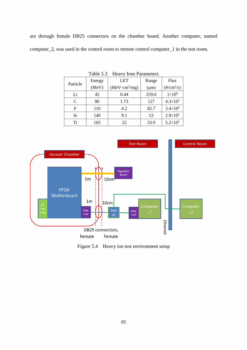
85
are through female DB25 connectors on the chamber board. Another computer, named
computer_2, was used in the control room to remote control computer_1 in the test room.
Table 5.3 Heavy Ions Parameters
Particle Energy
(MeV)
LET
(MeV·cm2/mg)
Range
(μm)
Flux
(#/cm2/s)
Li 45 0.44 259.6 1×10⁶
C 80 1.73 127 4.3×10⁵
F 110 4.2 82.7 3.4×10⁴
Si 140 9.1 53 2.9×10⁵
Ti 165 22 33.9 5.2×10⁵
Figure 5.4 Heavy ion test environment setup
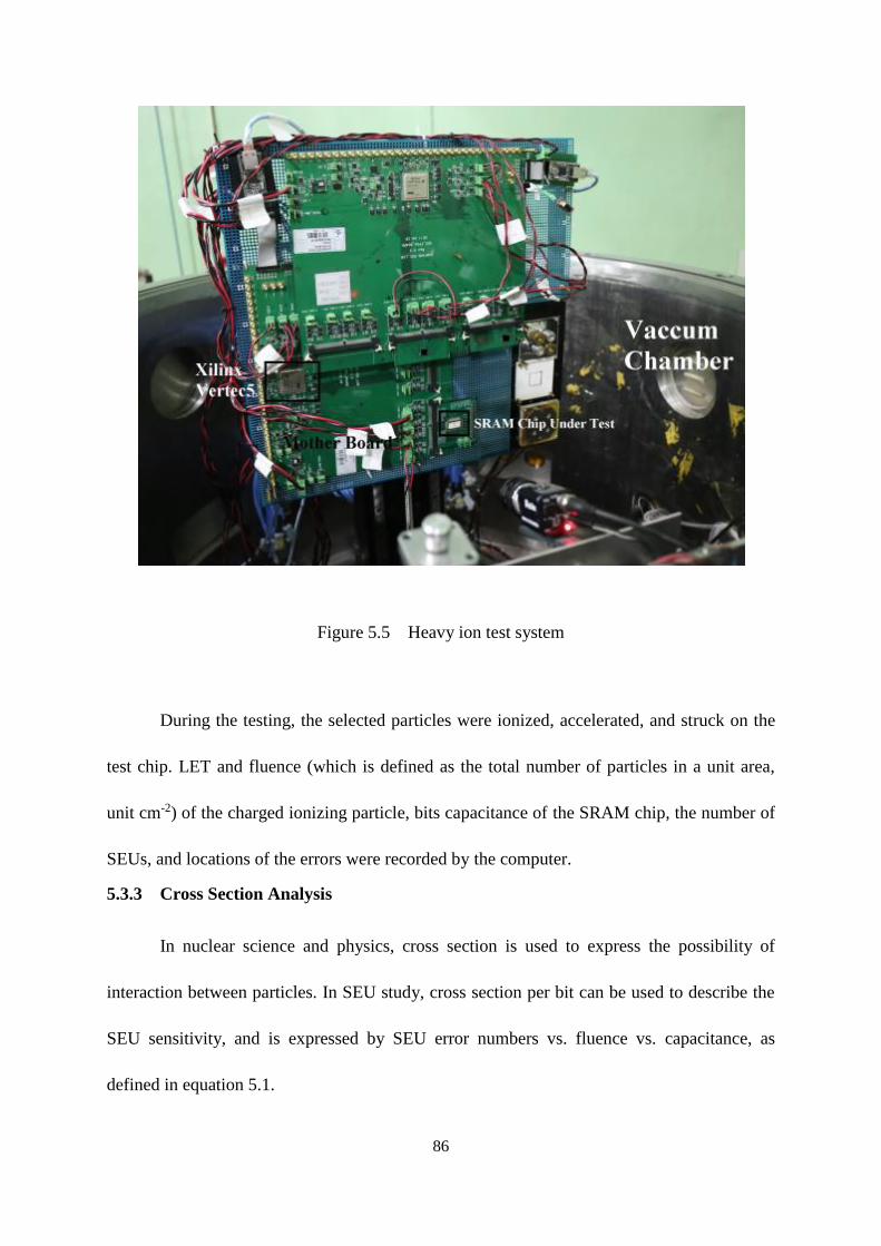
86
Figure 5.5 Heavy ion test system
During the testing, the selected particles were ionized, accelerated, and struck on the
test chip. LET and fluence (which is defined as the total number of particles in a unit area,
unit cm-2) of the charged ionizing particle, bits capacitance of the SRAM chip, the number of
SEUs, and locations of the errors were recorded by the computer.
5.3.3 Cross Section Analysis
In nuclear science and physics, cross section is used to express the possibility of
interaction between particles. In SEU study, cross section per bit can be used to describe the
SEU sensitivity, and is expressed by SEU error numbers vs. fluence vs. capacitance, as
defined in equation 5.1.
87
𝜎 = 𝑁𝐸𝑣𝑒𝑛𝑡/(𝐹 ∗ 𝑉) 5.1
Here, NEvent is total amount of upsets, F is particle fluence, and V is the volume of
irradiated devices (size of an SRAM array). The particle fluence F and volume V can be
treated as known and fixed parameters. The random characteristic of cross section comes
from Nevent. Under a similar radiation condition, the amount of upsets of digital cells is a
discrete random variable, which follows Poisson distribution with an expectation λ and
variance σ2. According to Central Limit Theorem, the number of tests times is large enough,
Poisson distribution can be considered as Normal distribution. For Normal distribution, 2σ error
bar means that the random variable has a probability of 95.4% to remain in the [μ-2σ, μ+2σ]
range.
From equation 5.1, cross section per bit with a 2σ error bar can be calculated for each
test case and the results are outlined in Figure 5.4. In the figure, data points at each supply
voltage are purposely offset in the horizontal direction to distinguish the corresponding error
bars. Zero data points, which signify that no SEU occurs, are indicated with arrows pointing
to the x axis.
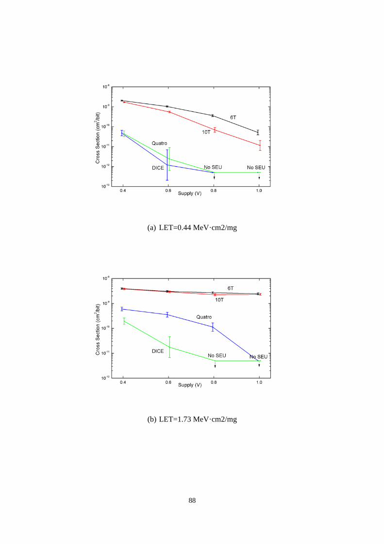
88
(a) LET=0.44 MeV·cm2/mg
(b) LET=1.73 MeV·cm2/mg
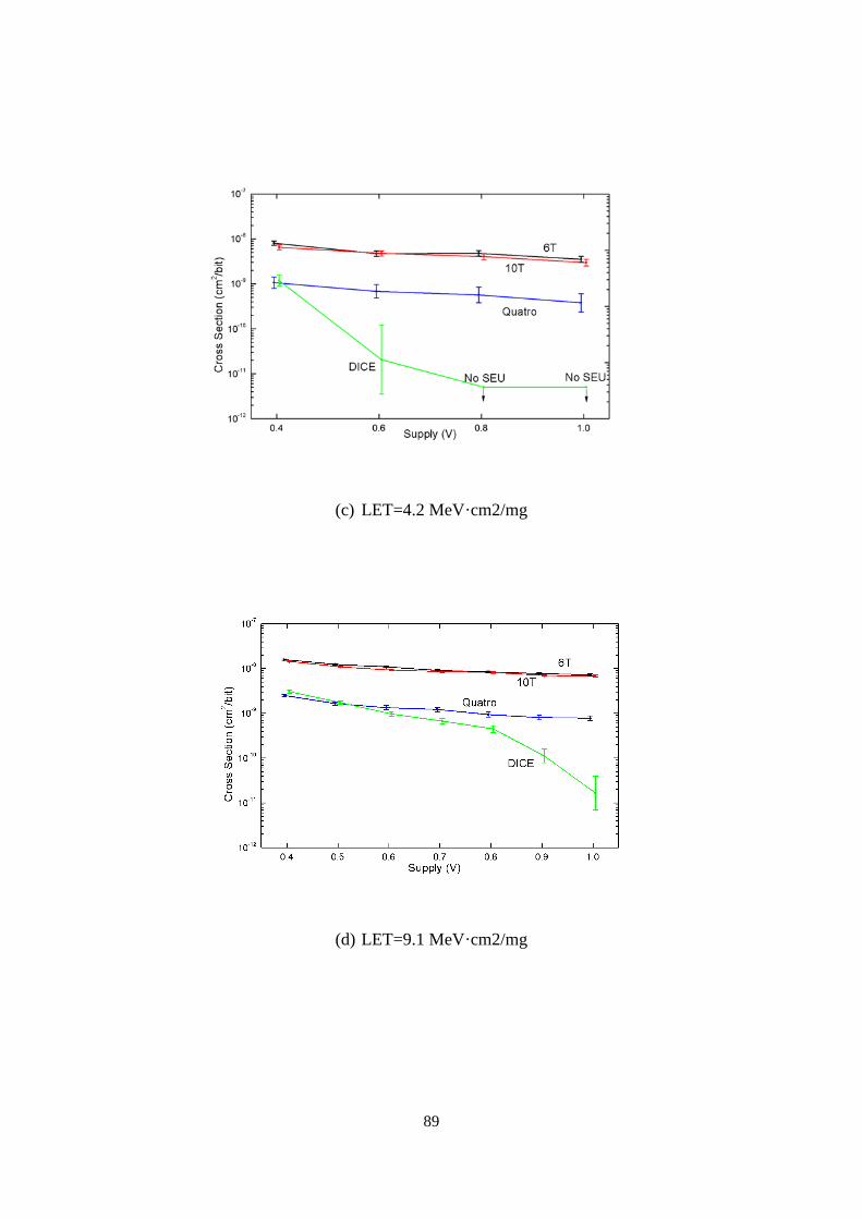
89
(c) LET=4.2 MeV·cm2/mg
(d) LET=9.1 MeV·cm2/mg
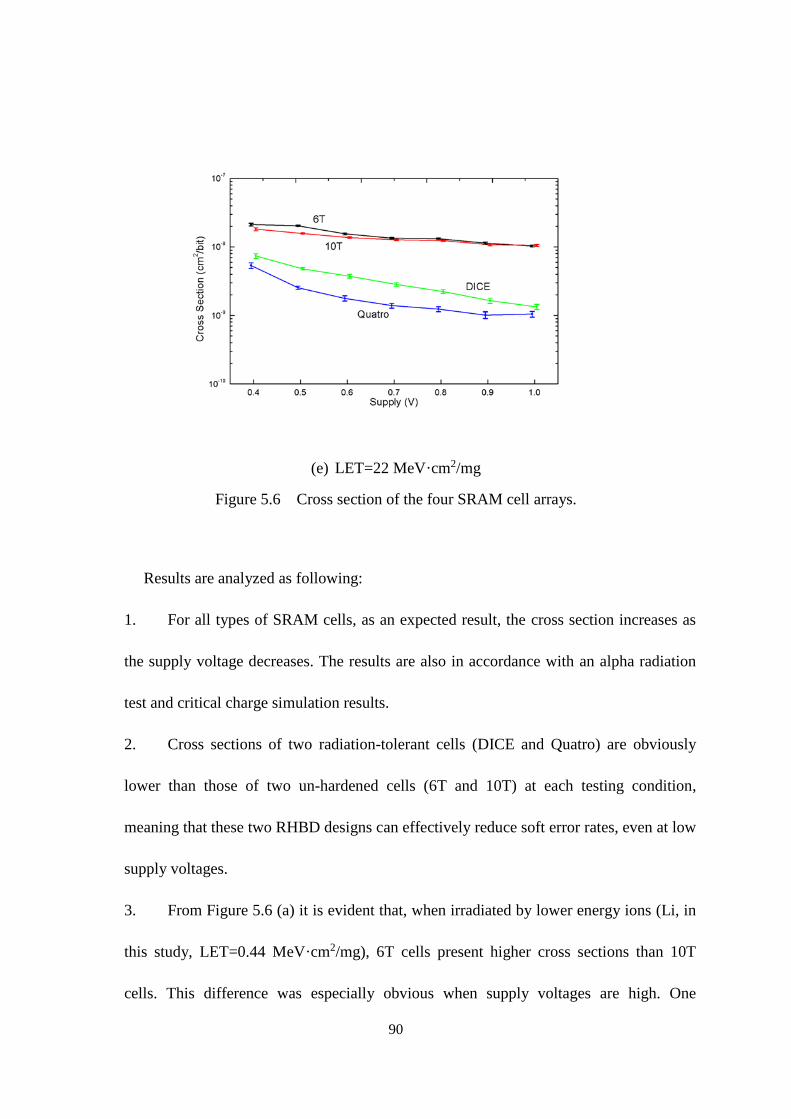
90
(e) LET=22 MeV·cm2/mg
Figure 5.6 Cross section of the four SRAM cell arrays.
Results are analyzed as following:
1. For all types of SRAM cells, as an expected result, the cross section increases as
the supply voltage decreases. The results are also in accordance with an alpha radiation
test and critical charge simulation results.
2. Cross sections of two radiation-tolerant cells (DICE and Quatro) are obviously
lower than those of two un-hardened cells (6T and 10T) at each testing condition,
meaning that these two RHBD designs can effectively reduce soft error rates, even at low
supply voltages.
3. From Figure 5.6 (a) it is evident that, when irradiated by lower energy ions (Li, in
this study, LET=0.44 MeV·cm2/mg), 6T cells present higher cross sections than 10T
cells. This difference was especially obvious when supply voltages are high. One
91
possible explanation is due to the extra transistors in 10T cells. Recall the schematic of
the 6T cell and 10T cell in Figure 3.3 and Figure 3.4. As compared to the 6T cell, the
10T cell has one additional transistor at each side, named N5 and N6, which are
connected to storage nodes Q and QB, respectively. According to equation 4.1, increased
capacitance on the node will consequently increase the critical charge. This additional
capacitance enhances radiation tolerance of 10T cells compared to 6T cells. This benefit
is especially obvious when supply voltage is 1 V, say a 4.5 times smaller cross section.
However, in cases of larger LETs and smaller supply voltages, this benefit becomes
almost negligible, which also explains the fact that the differences between cross sections
of 6T and 10T not significant enough for other ions except Li. For all other particles
except Li, the 2σ error bars associated with these data points of 6T and 10T cell are
largely overlapped. Hence, it is difficult to determine which one is more reliable than the
other according to this data.
4. In Figure 5.6 (a, b, c), it can be observed that with relatively low LET (Li, C, F),
cross sections of the DICE cell are smaller than the Quatro cell, especially when the
supply voltage is larger than 0.6 V. Based on the results, it can be concluded that the
DICE cell is more reliable than the Quatro cell with lower energy particles. This can be
explained by single-node upsets, as described in Chapter 4.1.2. Unlike the DICE cell, the
Quatro cell is not fully single-node upset tolerant.
In Figure 5.4 (d), when supply voltage goes under 0.6 V, the cross section of DICE
cells show no significant advance compared to Quatro cells. When it comes to high LET
radiation conditions, for example, LET=22 MeV·cm2/mg (e), DICE cells begin to lose in
92
the reliability competition with Quatro cells for all power supply ranges, as shown in
Figure 5.4(e). This phenomenon can be explained by SEEs charge spreading, which
could induce multi-node upsets (MNUs) inside a single cell and multi-bit upsets (MBUs)
in the array. DICE cells are not multi-node upset tolerant, since DICE presents more
sensitive node pairs than Quatro for double-node upsets [27]. Both MNUs and MBUs
would obviously degrade the single-event robustness of SRAM arrays and lead to larger
cross sections.
MNUs inside a memory cell cannot be identified, however, MBUs can be quite
easily observed, considering the fact that the location of each cell upset in each read
cycle can be recognized and recorded. Based on the experimental results, cross sections
induced by SBUs and MBUs were further separated to observe contribution of SBUs and
MBUs to the total cross sections shown in Table 5.4. For LET=22 MeV•cm2/mg, MBUs
induced cross sections of DICE cells are larger than those of Quatro cells with most
supply voltages, especially in a low supply voltage range. This result indicates that
Quatro cells are more robust to charge spreading than DICE cells, which also supports
the conclusion given above. From Table 5.4, it can be discerned that the DICE cells also
have larger SBUs contributed cross sections for all supply voltages when LET=22
MeV•cm2/mg. According to the SBUs cross sections data, it can be inferred that the
MNUs inside the DICE cell play an indispensable role to its single-event robustness
degradation, which is consistent with the work presented in [27].
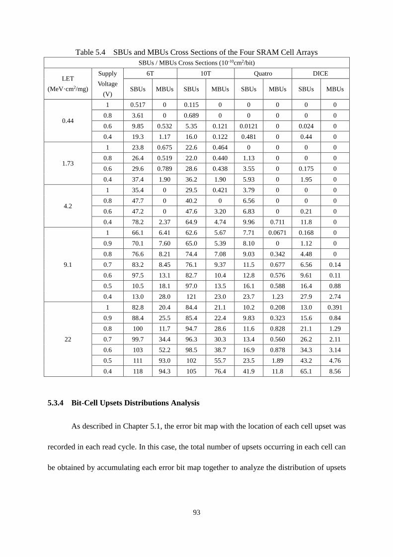
93
Table 5.4 SBUs and MBUs Cross Sections of the Four SRAM Cell Arrays
SBUs / MBUs Cross Sections (10-10cm2/bit)
LET
(MeV·cm2/mg)
Supply
Voltage
(V)
6T 10T Quatro DICE
SBUs MBUs SBUs MBUs SBUs MBUs SBUs MBUs
0.44
1 0.517 0 0.115 0 0 0 0 0
0.8 3.61 0 0.689 0 0 0 0 0
0.6 9.85 0.532 5.35 0.121 0.0121 0 0.024 0
0.4 19.3 1.17 16.0 0.122 0.481 0 0.44 0
1.73
1 23.8 0.675 22.6 0.464 0 0 0 0
0.8 26.4 0.519 22.0 0.440 1.13 0 0 0
0.6 29.6 0.789 28.6 0.438 3.55 0 0.175 0
0.4 37.4 1.90 36.2 1.90 5.93 0 1.95 0
4.2
1 35.4 0 29.5 0.421 3.79 0 0 0
0.8 47.7 0 40.2 0 6.56 0 0 0
0.6 47.2 0 47.6 3.20 6.83 0 0.21 0
0.4 78.2 2.37 64.9 4.74 9.96 0.711 11.8 0
9.1
1 66.1 6.41 62.6 5.67 7.71 0.0671 0.168 0
0.9 70.1 7.60 65.0 5.39 8.10 0 1.12 0
0.8 76.6 8.21 74.4 7.08 9.03 0.342 4.48 0
0.7 83.2 8.45 76.1 9.37 11.5 0.677 6.56 0.14
0.6 97.5 13.1 82.7 10.4 12.8 0.576 9.61 0.11
0.5 10.5 18.1 97.0 13.5 16.1 0.588 16.4 0.88
0.4 13.0 28.0 121 23.0 23.7 1.23 27.9 2.74
22
1 82.8 20.4 84.4 21.1 10.2 0.208 13.0 0.391
0.9 88.4 25.5 85.4 22.4 9.83 0.323 15.6 0.84
0.8 100 11.7 94.7 28.6 11.6 0.828 21.1 1.29
0.7 99.7 34.4 96.3 30.3 13.4 0.560 26.2 2.11
0.6 103 52.2 98.5 38.7 16.9 0.878 34.3 3.14
0.5 111 93.0 102 55.7 23.5 1.89 43.2 4.76
0.4 118 94.3 105 76.4 41.9 11.8 65.1 8.56
5.3.4 Bit-Cell Upsets Distributions Analysis
As described in Chapter 5.1, the error bit map with the location of each cell upset was
recorded in each read cycle. In this case, the total number of upsets occurring in each cell can
be obtained by accumulating each error bit map together to analyze the distribution of upsets
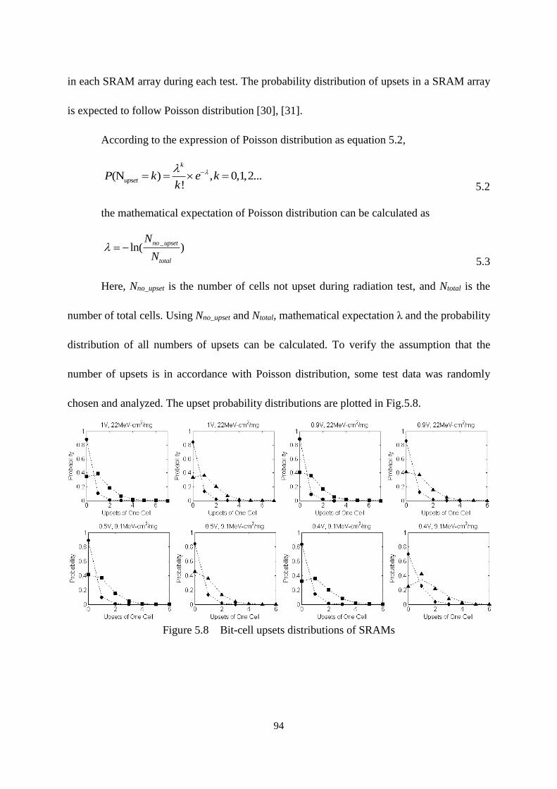
94
in each SRAM array during each test. The probability distribution of upsets in a SRAM array
is expected to follow Poisson distribution [30], [31].
According to the expression of Poisson distribution as equation 5.2,
5.2
the mathematical expectation of Poisson distribution can be calculated as
5.3
Here, Nno_upset is the number of cells not upset during radiation test, and Ntotal is the
number of total cells. Using Nno_upset and Ntotal, mathematical expectation λ and the probability
distribution of all numbers of upsets can be calculated. To verify the assumption that the
number of upsets is in accordance with Poisson distribution, some test data was randomly
chosen and analyzed. The upset probability distributions are plotted in Fig.5.8.
Figure 5.8 Bit-cell upsets distributions of SRAMs
(N ) , 0,1,2...!
k
upsetP k e kk
_ln( )
no upset
total
N
N
95
These figures present the probability distribution of four cells in four conditions, 1 V
with LET=22 MeV·cm2/mg, 0.9 V with LET=22 MeV·cm2/mg, 0.5 V with LET=9.1
MeV·cm2/mg, and 0.5 V with LET=9.1 MeV·cm2/mg, In all sub-figures, the symbols ■, ●
, ▲, and ◆ represent data points of 6T, Quatro, 10T, and DICE, respectively. The solid
dots represent the probability distribution discerned from tests results, while the dotted lines
show the corresponding Poisson distributions theoretically predicted from equations 5.1 and
5.2.
As depicted in Figure 5.8, all of the experimental data is in accordance with the
respective theoretical probability distributions. In fact, the expectation λ obtained can also be
used to describe the SEUs sensitivity memory cell operated and irradiated in a certain
condition. A larger λ indicates a lower SEU robustness. The test and calculated results
presented in Figure 5.8 further substantiate that Poisson distribution can be employed as a
tool to describe the statistic behavior of bit-cell upsets in SRAM arrays, which could also
build a foundation for applying Poisson distribution to generate SEU-like fault injections for
simulations.
96
CHAPTER 6
CONCLUSION AND FUTURE WORK
6.1 Conclusions
To study the supply voltage dependence of SEU on SRAM, this work presents the
alpha and heavy ion test results of four types of SRAMs: 6T, 10T, Quatro, and DICE,
fabricated on a 65 nm 1 V process. These SRAMs have been operated with different supply
voltages ranging from standard 1 V to sub-threshold 0.4 V, and also irradiated by alpha
particles and heavy ions with various LETs (0.44, 1.73, 4.2, 9.1, and 22 MeV•cm2/mg). Both
alpha and heavy ion radiation results demonstrate accordance with the simulation results.
Single-bit upset and multi-bits upset on four types of memory cells, as well as the bits-cell
upset distribution were also investigated and analyzed.
One common trend for all SRAMs is the fact that the decrease of supply voltage
increases their sensitivities to SEEs, which is mainly a result of the reduction of critical
charge. This trend should be given more attention, considering the fact that low voltage
operation is currently a popular method for large scale SRAMs design to reduce power, and
SRAMs’ increased SEEs susceptibilities can be a serious threat to reliable applications in
radiation environments.
According to our test results, the radiation-hardened DICE and Quatro cells remain a
more reliable option than the unhardened 6T and 10T cells in the near sub-threshold and
sub-threshold regions. The winner of the reliability competition between DICE and Quatro
depends on both supply voltage and LET. With lower LETs, DICE presents more optimal
97
reliabilities, considering the fact that it is completely hardened against single-node upsets,
whereas Quatro cell is not. However, in the case where LET increases to 9.1 MeV•cm2/mg
and supply voltage drops to lower than 0.6 V, or LET=22 MeV•cm2/mg for all supply
voltages, Quatro performs better than DICE. Analysis on SBUs and MBUs revealed that the
possible explanation for this phenomenon is that the DICE cell operated with relatively lower
supply voltages and/or irradiated with relatively higher LETs demonstrates more
consequential sensitivities to SEEs charge spreading than the Quatro cell. Charge spreading
induced MNUs and MBUs finally contribute to the larger cross sections of DICE.
Poisson distribution is applied to analyze the statistic behavior of bit-cell upsets in all
SRAMs. There is evidence that the actual upset distributions in the four SRAM arrays fit
their theoretically predicted Poisson distributions very well. This conclusion can also serve as
the foundation of applying Poisson distribution to generate SEU-like fault injections for
simulations.
6.2 Future work
In this work, the SRAM was not fully functional in a subthreshold region. Thus, when
the supply voltage was lower than 0.7 V, functional errors began to occur. This thesis
analyzed the results and proposed an improvement strategy in order to resolve this problem.
Future research should be conducted to improve the design and make it fully functional for
all superthreshold and subthreshold voltages.
This paper explored the supply voltage dependence of SEU in four different cells. The
new radiation hardened cell by design and the new radiation tolerant cell by layout technique
will be a promising work, utilizing the SRAM structure and test system.
98
The capacity of the SRAM is 4K×4 bits in this project, and significantly smaller than
SRAM used in modern digital systems. This is especially applicable in cases of signal
processing and data collection systems, both of which require a large capacity SRAM.
Therefore, designing subthreshold SRAM with larger capacity is also an interesting research
objective that can be explored in the future.
99
REFERENCES
[1] Andrei Pavlov and Manoj Sachdev, CMOS SRAM Circuit Design and Parametric Test in
Nano-Scaled Technologies, Springer, 2008, pp.1-2.
[2] Neil H.E.Weste and David Money Harris, Integrated Circuit Design (Fourth Edition),
Publishing House of Electronics Industry, 2011, pp.475-478.
[3] Benton H. Calhoun and Anantha P. Chandrakasan, “Static Noise Margin Variation for
Sub-threshold SRAM in 65-nm CMOS”, IEEE J. Solid-State Circuits, vol. 41, no.7, pp.
1673- 1679, July. 2006.
[4] Benton H. Calhoun and Anantha Chandrakasan, “A 256kb Sub-threshold SRAM in 65nm
CMOS”, in IEEE ISSCC Dig. Tech. Papers, 2006, pp.2592-2601.
[5] Benton Highsmith Calhoun and Anantha P. Chandrakasan, “A 256-kb 65-nm
Sub-threshold SRAM Design for Ultra-Low-Voltage Operation”, IEEE J. Solid-State
Circuits, vol.42, no.3, pp. 680-688, Mar. 2007.
[6] Sina Hassanzadeh, Milad Zamani, Khosrow Hajsadeghi, and Roghayeh Saeidi, “A Novel
Low Power 8T-cell Sub-threshold SRAM with Improved Read-SNM”, in Proc.
International Conference on Design & Technology of Integrated Systems in Nanoscale
Era, 2013, pp.35-38.
[7] P. Roche, J. M. Palau, C. Tavernier, G. Bruguier, R. Ecoffet, and J. Gasiot,
“Determination of key parameters for SEU occurrence using 3-D full cell SRAM
simulations,” IEEE Trans. Nucl. Sci., vol. 46, no. 6, pp. 1354–1362, Dec. 1999.
100
[8] J. M. Palau et al., “Device simulation study of the SEU sensitivity of SRAMs to internal
ion tracks generated by nuclear reactions,” IEEE Trans. Nucl. Sci., vol. 48, no. 2, pp.
225–231, Apr. 2001.
[9] Shah M. Jahinuzzaman, Mohammad Sharifkhani, and Manoj Sachdev, “An Analytical
Model for Soft Error Critical Charge of Nanometric SRAMs”, IEEE Trans. Very Large
Scale Integr. (VLSI) Syst., vol.17, no.9, pp. 1187-1195, Sept. 2009.
[10] Naveen Verma and Anantha P. Chandrakasan, “A 256 kb 65 nm 8T Subthreshold SRAM
Employing Sense-Amplifier Redundancy”, IEEE J. Solid-State Circuits, vol.43, no.1,
pp.141-149, Jan. 2008.
[11] Tae-Hyoung Kim, Jason Liu, John Keane, and Chris H. Kim, “A 0.2 V, 480 kb
Subthreshold SRAM With 1 k Cells Per Bitline for Ultra-Low-Voltage Computing”,
IEEE J. Solid-State Circuits, vol.43, no.2, pp.518-529, Feb. 2008.
[12] Jinhui Chen, Lawrence T. Clark, and Tai-Hua Chen, “An Ultra-Low-Power Memory
With a Subthreshold Power Supply Voltage”, IEEE J. Solid-State Circuits, vol.41, no. 10,
pp.2344-2353, Oct. 2006.
[13] Ik Joon Chang, Jae-Joon Kim, Sang Phill Park, and Kaushik Roy, “A 32 kb 10T
Sub-Threshold SRAM Array With Bit-Interleaving and Differential Read Scheme in 90
nm CMOS”, IEEE J. Solid-State Circuits,vol.44, no.2, pp.650-658, Feb. 2009.
[14] Ming-Hsien Tu, et al., “A Single-Ended Disturb-Free 9T Subthreshold SRAM With
Cross-Point Data-Aware Write Word-Line Structure, Negative Bit-Line, and Adaptive
Read Operation Timing Tracing”, IEEE J. Solid-State Circuits, vol.47, no.6,
pp.1469-1482, June. 2012.
101
[15] Yi-Wei Chiu, et al., “40 nm Bit-Interleaving 12T Subthreshold SRAM With Data-Aware
Write-Assist”, IEEE Trans. Circuits Syst. I, Reg. Papers, vol.61, no.9, pp.2578-2585,
Sept. 2014.
[16] T. Calin, M. Nicolaidis, and R. Velazco, “Upset Hardened Memory Design for
Submicron CMOS Technology”, IEEE Trans. Nucl. Sci., vol.43, no.6, pp.2874-2878,
Dec. 1996.
[17] Shah M. Jahinuzzaman, David J. Rennie, and Manoj Sachdev, “A Soft Error Tolerant
10T SRAM Bit-Cell With Differential Read Capability”, IEEE Trans. Nucl. Sci., vol.56,
no.6, pp.3768-3773, Dec. 2009.
[18] Guohe Zhang, Jun Shao, Feng Liang, and Dongxuan Bao, “A novel single event upset
hardened CMOS SRAM cell”, IEICE Electronics Express, vol.9, no.3, pp.140-145, Feb.
2012.
[19] P. Hazucha, T. Karnik, J. Maiz, S. Walstra, B. Bloechel, J. Tschanz, G. Dermer, S.
Hareland, P. Armstrong, and S. Borkar, “Neutron Soft Error Rate Measurements in a
90-nm CMOS Process and Scaling Trends in SRAM from 0.25-mm to 90-nm
Generation,” in Proc. IEDM Tech. Dig., Dec. 2003, pp. 21.5.1–21.5.4.
[20] Hiroshi Fuketa, Masanori Hashimoto, Yukio Mitsuyama, and Takao Onoye,
“Alpha-Particle-Induced Soft Errors and Multiple Cell Upsets in 65-nm 10T Subthreshold
SRAM,” in Proc. IEEE Int. Reliab. Phys. Symp., May. 2010, pp. 213–217.
[21] Hiroshi Fuketa, Masanori Hashimoto, Yukio Mitsuyama, and Takao Onoye,
“Neutron-Induced Soft Errors and Multiple Cell Upsets in 65-nm 10T Subthreshold
SRAM,” IEEE Trans. Nucl. Sci., vol.58, no.4, pp. 2097- 2102, Aug. 2011.
102
[22] Paul E. Dodd and Lloyd W. Massengill, “Basic Mechanisms and Modeling of
Single-Event Upset in Digital Microelectronics,” IEEE Trans. Nucl. Sci., vol.50, no.3, pp.
583-602, Jun. 2003.
[23] Jan M. Rabaey, Anantha Chandrakasan, Borivoje Nikolic. “Digital Integrated Circuits-A
Design Perspective, Second Edition.” 658-661.
[24] Neil H. E. Weste, David Money Harris. “Integrated Circuit Design, Fourth Edition.”
458-460.
[25] Leland Chang, Robert K. Montoye, Yutaka Nakamura etc. “ An 8T-SRAM for
Variability Tolerance and Low-Voltage Operation in High-Performance Caches,” IEEE
Journal of Solid-state circuit, vol.43, no.4, Apr 2008.
[26] Y.Morita et al., “A Vth-variation-tolerant SRAM with 0.3-V minimum operation voltage
for memory-rich SoC under DVS environment,” Proc. VLSI Circuits Symp., 2006, pp.
13-14.
[27] K.Zhang et al., “A 2-GHz 70-mb SRAM in 65-nm CMOS technology with integrated
column-based dynamic power supply,” JSSC, vol.41, no. 1, Jan. 2006, pp. 146-151.
[28] T. Kim, H. Eom, J. Keane, and C. Kim, “Utilizing reverse short channel effect for
optimal subthreshold circuit design,” in Proc. Int. Symp. Low Power Electronics
(ISLPED’06), Oct. 2006, pp. 127–130.
[29] Robert C. Baumann. “Radiation-Induced Soft Errors in Advanced Semiconductor
Technologies,” IEEE Trans. On Device and Materials Reliability, Vol. 5, NO. 3, Sep.
2005, pp. 305-316.
103
[30] J. Bisgrove, J. Lynch, P. McNulty, W. Abdel-Kader, V. Kletnieks and W.
Kolasinski,“Comparison of Soft Errors Induced By Heavy Ions And Protons,” IEEE
Transactions onNuclear Science, Vol. NS-33, No. 6, pp. 1571-1576, Dec. 1986
[31] J. S. Fu, C. L. Axness and H. T. Weaver, “Memory SEU simulations using 2-D
transportcalculations,” IEEE Electron Dev. Lett., Vol. EDL-6, No. 8, pp. 422-424, 1985
[32] C.L. Axness, H. T. Weaver, and J. S. Fu, “Mechanisms Leading to Single Event
Upset,”IEEE Transactions on Nuclear Science, Vol. NS-33, No. 6, pp. 1577-1580, 1986
[33] J. A. Zoutendyk, L. S. Smith, G. A. Soli and R. Y. Lo, “Experimental Evidence For a
NewSingle-Event Upset (SEU) Model in a CMOS SRAM Obtained From Model
Verification,”IEEE Transactions on Nuclear Science, Vol. NS-34, No. 6, pp. 1292-1299,
1987
[34] R. L. Woodruff and P. J. Rudeck, “Three-Dimensional Numerical Simulation of
SingleEvent Upset of an SRAM Cell,” IEEE Transactions on Nuclear Science, Vol. 40,
No. 6, pp.1795-1803, 1993
[35] P. E. Dodd and L. W. Massengill, “Basic Mechanisms and Modeling of Single-Event
Upset in Digital Microelectronics,” IEEE Transactions on Nuclear Science, Vol. 50, No.
3, pp. 583-602, Jun. 2003
[36] P. E. Dodd, F. W. Sexton, G. L. Hash, M. R. Shaneyfelt, B. L. Draper, A. J. Farino, and
R. S. Flores, “Impact of technology trends on SEU in CMOS SRAMs,” IEEE Trans.
Nucl. Sci., vol. 43, pp. 2797–2804, Dec. 1996.
[37] H. T. Weaver, C. L. Axness, J. D. McBrayer, J. S. Browning, J. S. Fu, A. Ochoa1, Jr., R.
Koga, “An SEU Tolerant Memory Cell Derived From Fundamental Studies of SEU
104
Mechanisms in SRAM,” IEEE Transactions on Nuclear Science, Vol. NS-34, No. 6,
pp.1281-1286, Dec. 1987
[38] Shah M. Jahinuzzaman, David J. Rennie, and Manoj Sachdev, “A Soft Error Tolerant
10T SRAM Bit-Cell With Differential Read Capability,” IEEE Transactions on Nuclear
Science, Vol. 56, No. 6, pp. 3768-3773, Dec. 2009
[39] S. Jagannathan, T. D. Loveless, B. L. Bhuva, S.-J. Wen, R. Wong, M. Sachdev, D.
Rennie, and L. W. Massengill, “Single-Event Tolerant Flip-Flop Design in 40-nm Bulk
CMOS Technology”, IEEE Trans. Nucl. Sci., vol.58, no.6, pp.3033-3037, Dec. 2011.
[40] Kuande Wang. “Ultra Low-Power Fault-Tolerant SRAM Design in 90nm CMOS
Technology.” Thesis for Master of Science, University of Saskatoon, 2010,
[41] Sven Lütkemeier, Ulrich Rückert. “A Subthreshold to Above-Threshold Level Shifter
Comprising a Wilson Current Mirror”, IEEE TRANSACTIONS ON CIRCUITS AND
SYSTEMS—II: EXPRESS BRIEFS, VOL. 57, NO. 9, pp. 721-724, SEPTEMBER 2010.