Supplement to Graphic Symbols for Electrical and ... Y32.2-1986 Sup.pdf · Graphic Symbols for...
66
adopted bV th e DEPARTMENT OF DEFENSE United St at es of America see inside front co ve r for acce pta nce not ice 12, 1986 ANSI/IEEE Std 315A-1986 (Supp leme nt to ANSI Y32 .2-197S , ANSI/ IEEE S td 315 -1975) JUL American National Standard IEEE Standard Supplement to Graphic Symbols for Electrical and Electronics Diagrams PU blished bv The In st it u te o f El ect rical and Electro n ics E ngi n eers, Inc 345 East 47t h St ree t, New York, NY 10017, USA 1993 S1I IOi44
Transcript of Supplement to Graphic Symbols for Electrical and ... Y32.2-1986 Sup.pdf · Graphic Symbols for...
adopted bV the
DEPARTMENT OF DEFENSE United States of America
see inside front cover for accepta nce notice
S~pltmber 12, 1986
ANSI/IEEE Std 315A-1986 (Supp lement to ANSI Y32.2-197S,
ANSI / IEEE Std 315-1975)
JUL
American National Standard
IEEE Standard
Supplement to
Graphic Symbols for
Electrical and Electronics
Diagrams
PU blish ed bv Th e In stit ute o f Electrica l a nd E lectro n ics E ngi neers, Inc
345 East 47t h Street , New York , NY 10017, USA
1993
S1I IOi44
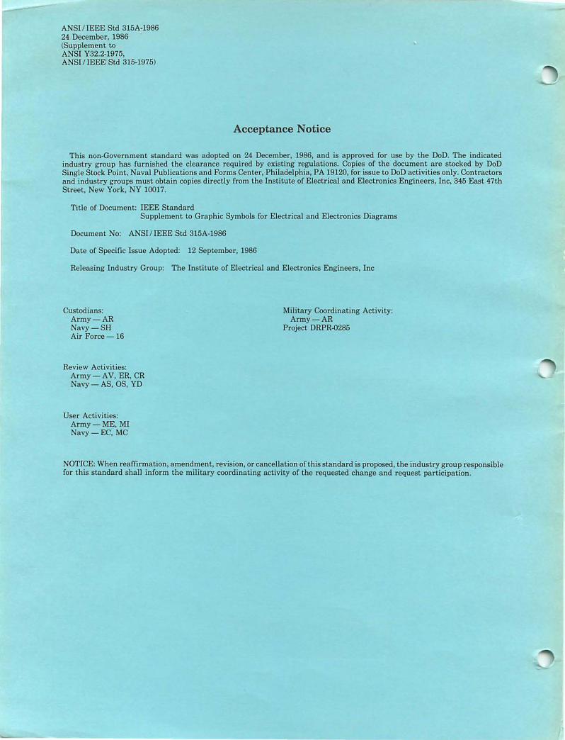
ANSI / IEEE Std 3ISA-1986 24 December, 1986 (Supplement to ANSI Y32.2-197S, ANSIIIEEE Std 315-1975)
Acceptance Notice
This non.Government standard wns adopted on 24 December, 1986, and is approved for use by the DoD. The indicated industry group has furnished the clearance required by existing regulations. Copies of the document are stocked by DoD Single Slack Point, Naval Publications and Forms Center, Philadelphia, PA 19120, for issue to 0 00 activities only. Contractors and industry groups must obtain copies directly from the Institute of Electrical and Electronics Engineers, Inc. 345 East 47th Street. New York, NY 10017.
Title of Document: IEEE Standard Supplement to Graphic Symbols for Electrical and Electronics Diagrams
Document No: ANSII IEEE Std 315A-1986
Date of Specific Issue Adopted: 12 September, 1986
Releasing Industry Group: The Institute of Electrical and Electronics Engineers, Inc
Custodians: Army-AR Navy-SH Air Force - 16
Review Activities: Army -AV. ER, CR Navy - AS, as, YD
User Activities: Army-ME, MI Navy -EC, MC
Military Coordinating Activity: Army-AR
Project DRPR-0285
NOTICE: When reaffirmation , amendment, revision, or cancellation of this standard is proposed, the industry group responsible for this standard shall inform the military coordinating activity of the requested change and request participation.
ANSI/IEEE Std 315A-1986 (Supplement to ANSI V32.2-1975,
ANSI/IEEE Std 315·1975)
American National Standard IEEE Standard
Supplement to Graphic Symbols for
Electrical and Electronics Diagrams
Sponsor IEEE Standards Coordinating Committee 11, Graphic Symbols
Institute of Electrical and Electronics Engineers
Approved September 19, 1985 Institute of Electrical and Electronics Engineers
Approved November 15, 1985 American National Standards Institute
© Copyright 1986 by
The Institute of Electrical and Electronics Engineers, Inc 345 East 47th Street, New York, NY 10017, USA
No part of this pUblication may be reproduced in any form, in an electronic retrieval system or otherwise,
without the prior written permission of the publisher.
IEEE Standards documents are developed within th~ Technical Committees of the IEEE Societies and the Standards Coordinating Committees of the IEEE Standards Board. Members of the committees serve voluntarily and without compensation. They are not necessarily members of the Institute. The standards developed within IEEE represent a consensus of the broad expertise on the subject within the Institute as well as those activities outside of IEEE which have expressed an interest in participating in the development of the standard.
Use of an IEEE Standard is wholly voluntary. The existence of an IEEE Standard does not imply that there are no other ways to produce, test, measure, purchase, market, or provide other goods and services related to the scope of the IEEE Standard. Furthermore, the viewpoint expressed at the time a standard is approved and issued is subject to change brought about through developments in the state of the art and comments received from users of the standard. Every IEEE Standard is subjected to review at least once every five years for revision or reaffirmation. When a document is more than five years old, and has not been reaffirmed, it is reasonable to conclude that its contents, although still of some value, do not wholly reflect the present state of the art. Users are cautioned to check to determine that they have the latest edition of any IEEE Standard.
Comments for revision of IEEE Standards are welcome from any interested party, regardless of membership affiliation with IEEE. Suggestions for changes in documents should be in the form of a proposed change of text, together with appropriate supporting comments.
Interpretations: Occasionally questions may arise regarding the meaning of portions of standards as they relate to specific applications. When the need for interpretations is brought to the attention of IEEE, the Institute will initiate action to prepare appropriate responses. Since IEEE Standards represent a consensus of all concerned interests, it is important to ensure that any interpretation has also received the concurrence of a balance of interests. For this reason IEEE and the members of its technical committees are not able to provide an instant response to interpretation requests except in those cases where the matter has previously received formal consideration.
Comments on standards and requests for interpretations should be addressed to:
Secretary, IEEE Standards Board 345 East 47th Street New York, NY 10017 USA
The individual symbols contained in this standard may be copied, reproduced, or employed in any fashion without permission of the IEEE. Any statement that the symbols used are in conformance with this standard shall be on the user's own responsibility.
~ '-.
-
Foreword
r (This Foreword is not a part of ANSI/IEEE Std 315A-1986, Supplement to Graphic Symbols for Electrical and Electronics Diagrams.)
This standard supplements ANSI/IEEE Std 315-1975 by providing symbols approved by the International Electrotechnical Commission since 1975, or for which there is now a greater need in the United States arising from international commerce. It is believed that immediate issue of this supplement is preferable to the inevitable delay that would occur if a complete and proper revision of ANSI/IEEE Std 315-1975 were undertaken.
Besides adding new symbols, some updating of the information in ANSI/IEEE Std 315-1975 has been undertaken. The updating includes references to other standards, IEC labels on symbols where a change has occured, and correction of errors.
This supplement is based on IEC Publication 617, Parts 2 through 11 and Part 13 as published in 1983. IEC Publication 617, Part 12 is included in full in ANSI/IEEE Std 91-1984, IEEE Standard Graphic Symbols for Logic Functions.
When this standard was approved SCC 11.1 had the following membership:
C. J. Andrasco I. M. Berger L. Burns R. Coel J. B. Deam L. Davis A. C. Gannett
G. A. Knapp J. M. Kreher F. R. Misiewicz C. R. Muller C. McCarthy R. Pinger A. I. Rubin L. Schulz
H. H. Seaman G. Shapiro J. W. Siefert S. V. Soanes R. M. Stern M. E. Taylor R. J. Yuhas
When this standard was approved the IEEE Standards Coordinating Committee on Letter and Graphic Symbols, SCC 11, had the following membership:
Robert B. Angus, Jr J. C. Brown John M. Carroll Gordon A. Knapp
Conrad R. Muller John B. Peatman J. William Siefert Thomas R. Smith
S. V. Soanes Roger M. Stern Leter H. Warren Steven A. Wasserman
When the IEEE Standards Board approved this standard on September 19, 1985, it had the following membership:
John E. May, Chairman
James H. Beall Fletcher J. Buckley Rene Castenschiold Edward Chelotti Edward J. Cohen Paul G. Cummings Donald C. Fleckenstein
- Member emeritus
John P. Riganati, Vice Chairman Sava I. Sherr, Secretary
Jay Forster Daniel L. Goldberg Kenneth D. Hendrix Irvin N. Howell Jack Kinn Joseph L. KoepfingerIrving Kolodny R. F. Lawrence
Second Printing February 1989
Lawrence V. McCall Donald T. MichaelFrank L. Rose Clifford O. Swanson J. Richard Weger W. B. Wilkens Charles J. Wylie
, Contents
SECTION PAGE
AAl Purpose ...................... 7 AA2 Scope ........................ 7 AA3 Organization .................. 7 AA4 References.................... 7
Section 1 Qualifying Symbols 1.1 Adjustability
Variability. . . . . . . . . . . . . . . . . . . .. 9 1.2 Special-Property Indicators. . . . . . . . .. 9 1.3 Radiation Indicators (electromagnetic
and particulate) . . . . . . . . . . . . . . .. 9 1.4 Physical-State Recognition Symbols .. " 9 1.7 Direction of Flow of Power, Signal,
or Information ................ 9 1.8 Kind of Current ................. 10 1.10 Envelope
Enclosure ..................... 10 1.14 Operational Dependence On a
Characteristic Quantity ........... 10 1.15 Signal Indentifiers ................ 10 1.16 Signal Waveforms ................ 10 1.17 Control by Nonelectrical Quantities .... 10
Section 2 Graphic Symbols for Fundamental Items (not included in other sections)
2.1 Resistor ...................... 11 2.2 Capacitor. . . . . . . . . . . . . . . . . . . . . 11 2.3 Antenna ...................... 11 2.4 Attenuator .................... 12 2.6 Delay Function
Delay Line Slow-Wave Structure .............. 12
2.9 Pickup
2.10 2.17 2.18 2.19
Head ........................ 12 Piezoelectric Crystal Unit ........... 12 Igniter Plug .................... 13 Ideal Circuit Elements ............. 13 Faults ........................ 13
Section 3 Graphic Symbols for Transmission Path 3.1 Transmission Path
Conductor Cable Wiring ....................... 13
3.2 Distribution Lines Transmission Lines ............... 14
3.6 Waveguide ...•................. 14 3.10 Pressure Tight Bulkhead Cable Gland
Cable Sealing End ................ 14
Section 4 Graphic Symbols for Contacts, Switches, Contactors, and Relays 4.1 4.3 4.6 4.14
4.21 4.22
4.29 4.34
4.35
Switching Function ............... 15 Basic Contact Assemblies ........... 15 Switch ....................... 17 Limit Switch Sensitive Switch ................. 17 Thermostat .................... 17 Flasher Self-Interrupting Switch ............ 17 Contactor . . . . . . . . . . . . . . . . . . . . . 17 Multipole and Multiposition
Switches ..................... 18 Switchgear and Control gear ......... 20
SECTION PAGE
4.36 Block Symbols for Motor Starters ..... 20 4.37 Operating Devices for
Electromechanical (all or nothing) Relays ...................... 20
Section 5 Graphic Symbols for Terminals and Connectors 5.3 Connector
Disconnecting Device Jack Plug ......................... 22
5.6 Coaxial Connector Coaxial Junction ................ 22
Section 6 Graphic Symbols for Transformers, Inductors, and '¥indings
6.1 Core ......................... 23 6.2 Inductor
Winding Reactor Radio-Frequency Coil Telephone Retardation Coil .. . . . . . . . 23
6.4 Transformer Telephone Induction Coil Telephone Repeating Coil .......... 23
6.6 Ferrite Cores - Symbol Elements ..... 26 6.7 Ferrite Cores ................... 27 6.8 Magnetic Storage Matrices
(Topographical Representation) ..... 27
Section 7 Graphic Symbols for Electron Tubes and Related Devices 7.1 Electron Tube .................. 28 7.3 Typical Applications .............. 29 7.4 Solion
Ion-Diffusion Device . . . . . . . 29 7.5 Coulomb Accumulator
Electrochemical Step-Function Device ... 29 7.7 Nuclear-Radiation Detector
Ionization Chamber Proportional Counter Tube Geiger-Miiller County Tube ......... 30
Section 8 Graphic Symbols for Semiconductor Devices 8.2 Element Symbols ................ 31 8.3 Special-Property Indicators .......... 31 8.5 Typical Applications, Two-Terminal
Devices ..................... 32 8.6 Typical Applications, Three- (or more)
Terminal Devices ............... 33 8.10 Photon-Coupled Isolator ........... 35 8.12 Ionizing Radiation Detectors ........ 35
Section 9 Graphic Symbols for Circuit Protectors 9.1 Fuse ......................... 36 9.3 Lightning Arrester
Arrester (electric surge) Gap ................ ' ......... 36
9.4 Circuit Breaker .................. 36 9.6 Protective Relays - Block
Symbols and Qualifying Symbol ..... 37 9.7 Examples of Protective Relays ....... 37 9.8 Other Relay Devices .............. 38
-
SECTION PAGE
Section 10 Graphic Symbols for Acoustic Devices 10.1 Audible-Signaling Device ........... 39
Section 11 Graphic Symbols for Lamps and Visual-Signaling Devices
11.1 Lamp ........................ 39 11.3 Electromechanical Signal ........... 39
Section 12 Graphic Symbols for Readout Devices 12.1 Meter
Instrument .................... 40 12.2 Electromagnetically Operated Counter
Message Register ................. 40 12.3 Indicating, Recording, and Integrating
Instruments, General Symbols ...... 40 12.4 Examples of Indicating Instruments .... 40 12.5 Examples of Recording Instruments .... 41 12.6 Examples of Integrating Instruments ... 41 12.7 Counting Devices ................ 41 12.8 Telemetering Devices .............. 42 12.9 Electric Clocks .................. 42
Section 13 Graphic Symbols for Rotating Machinery 13.1 Rotating Machine ................ 42 13.5 Applications: Alternating-Current
Machines .................... 42 13.6 Applications: Alternating-Current
Machines with Direct-Current Field Excitation ................... 42
Section 14 Graphic Symbols for Mechanical Functions 14.2 Mechanical Motion ............... 43 14.3 Clutch
Brake ........................ 43 14.4 Manual Control ................. 43 14.5 Detents, Latching, and Blocking ...... 44
Section 15 Graphic Symbols Commonly Used in Connection with VHF, UHF, and SHF Circuits 15.2 15.4
15.5 15.6 15.7 15.8 15.9
15.10 15.11 15.12
15.13 15.14 15.16 15.20 15.21
Coupling ...................... 45 Hybrid Directionally Selective Transmission
Devices ..................... 45 Mode Transducer . . . . . . . . . . . . . . . . 45 Mode Suppressor ................ 45 Rotary Joint ................... 45 Nonreciprocal Devices ............. 45 Resonator Tuned Cavity ................... 45 Resonator (Cavity-Type) Tube ....... 45 Magnetron ..................... 46 Velocity-Modulation (Velocity-
Variation) Tu be . . . . . . . . . . . . . . . . 46 Transmit-Receive (TR) Tube ......... 46 Traveling-Wave-Tube .............. 47 Filter ........................ 48 Multiport Devices ................ 48 Lasers and Masers ................ 48
SECTION PAGE
Section 16 Graphic Symbols for Composite Assemblies 16.1 Circuit Assembly
Circuit Subassembly Circuit Element ................. 49
16.2 Amplifier ..................... 49 16.9 Gyro
Gyroscope Gyrocompass . . . . . . . . . . . . . . . . . . . 49
16.13 Changer, General Symbol- Converter General Symbol ................ 49
16.14 Galvanic Separator ............... 49 16.15 Heat Source, General Symbol ........ 49 16.16 Generator, General Symbol ......... 49 16.17 Sensors and Detectors ............. 50 16.18 Applications of Sensors ............ 50
Section 17 Graphic Symbols for Analog and Digital Logic Functions 17.10 Analog Elements for
Computations and Control ......... 51
Section 18 Graphic Symbols for Digital Logic Functions No changes
Section 19 Graphic Symbols for SpecialPurpose Maintenance Diagrams No changes
Section 20 Graphic Symbols Commonly Used on System Diagrams, Maps, and Charts (Communications Equipment) 20.3 Exchange Equipment (Relocation of
20.3.2 and 20.3.3) .............. 53
Section 21 Graphic Symbols Commonly Used on System Diagrams, Maps, and Charts 21.1 Generating Station ............... 54 21.2 Hydroelectric Generating Station ...... 54 21.3 Thermoelectric Generating Station ..... 54 21.4 Prime Mover ................... 54 21.5 Substation ..................... 54 21.6 Wind Generating Station ........... 54 21. 7 Plasma Generating Station .......... 54
Section 22 Class Designation Letter No changes
Section 23 Referenced Standards
See AA4 ........................... 7
Section 24 Telecommunications Switching and Peripheral Equipment 24.1 Switching Systems ............... 55 24.2 Block Symbols for Switching
Equipment ................... 57 24.3 Qualifying Symbols for Transducers,
Recorders, and Reproducers. . . . . . . . 57 24.4 Recorders and Reproducers ......... 57
SECTION
Section 25 Telecommunications Transmission
PAGE
25.1 Amplified Circuits ............... 58 25.2 Qualifying Symbols for Pulse
Modulation ................... 58 25.3 Signal Generator, Waveform
Generator .................... 58 25.4 Changers, Converter, General
Symbol ..................... 58 25.5 Filters ....................... 59 25.6 Networks ..................... 59
SECTION PAGE
25.7 25.8 25.9 25.10
25.11 25.12
25.13
25.14
Electronic Chopping Device ......... 59 Threshold Devices ................ 59 Terminating Sets ................ 60 Modulator, Demodulator,
Discriminator ................. 60 Concentrators, Multiplexers ......... 60 Frequency Spectrum Diagram
Symbol Elements ............... 61 Examples of Frequency Spectrum
Diagrams ... . . . . . . . . . . . . . . . . . 61 Fiber Optic Devices ............... 62
-
American National Standard IEEE Standard
Supplement to Graphic Symbols for
Electrical and Electronics Diagrams
AAl. Purpose
This supplement is intended to provide additional graphic symbols and information on internationally approved graphic symbols needed for use for electrical and electronics diagrams_
AA2_ Scope
This supplement provides graphic symbols for use on all electrical or electronics diagrams except for those required for
(1) Logic circuit diagrams_ See ANSI/IEEE Std 91-1984 [4]1_
(2) Architectural plans. See ANSI Y32.9-1972 [2] and IEC Publication 617 (1983) [22] Part 11, ch IV.
(3) Street maps and building system layouts for cable TV application . See ANSI/IEEE Std 623-1976 [8] and IEC Publicatiun 617 (1983) [22) ,Part 11, ch III.
AA3_ Organization
This supplement places the IEC Publication 617 new material in a practical sequence with related material in ANSI/IEEE Std 315-1975 [7) . Except where the nature of the. revisions dictate otherwise (for reasons of clanty) eXIsting ANSI/IEEE Std 315-1975 [7) text is not
repeated.
1 Numbers in brackets correspond to those of the references listed in Sect ion AA4.
1
AA4. References
This standard shall be used in conjunction with the following publications:
[1) ANSI Yl.l -1972 (R 1984), Abbreviations for Use On Drawings and In Text.'
[2] ANSI Y32.9-1972, American National Standard Graphic Symbols for Electrical Wiring and Layout Diagrams Used in Architecture and Building Construction.
[3] ANSI/IEEE Std C37.2-1979, IEEE Standard Electrical Power System Device Function Numbers. 3
[4] ANSI/IEEE Std 91-1984, IEEE Standard Graphic Symbols for Logic Functions.
[5) ANSI/IEEE Std 260-1978, IEEE Standard Letter Symbols for Units of Measurement.
[6] ANSI/IEEE Std 280-1985, IEEE Standard Letter Symbols for Quantities Used in Electrical Science and Electrical Engineering.
[7] ANSI/IEEE Std 315-1975, Graphic Symbols for Electrical and Electronics Diagrams.
[8] ANSI/IEEE Std 623-1976, Graphic Symbols for Grid and Mapping Diagrams Used in Cable Television Systems.
:2 ANSI publicat ions are available from th~ Sales De· partment, American National S tandards Institute, ] 430 Broadway , New York, NY 1001 8. .
3 1EEE publications are available from IEEE Sen'lce Center, 445 Hoes Lane, Piscataway, NJ 08854 .
---
SECTIO N 1 1.7.7 to 1.l7A
1. 7.7 Reception
See NOTE 1.7.6A
lEe ----o):>-~.o--
1.7.8 Energy fl ow from th e busbars
lEe I )
1.7.9 Energy flow towards the busbars
lEe 1-1 --<:(;---
1.7.10 Bidirectional energy now
1.8.1 Add:
lEe I ()
The voltage may be ind icated at th e r ight of the symbol and the type of sys tem at t he left .
1.8.1.1 Appl icat io n : Direct current , three conductors including midwire, 220 V (110 V between each o uter conductor and midwi re )
2M may be replaced by 2 + M
lEe 2M - 220 / 110V
1.8 .2 Alte rnat ing current
lEe """
Add:
The numerical value of the frequency or the freque ncy ra nge m ay be added at the r ight- hand side o f t he sym bol.
Th e vo ltage may also be indicated to the right of the sym bol.
The number of phases and the presence of a neutral may be indicated a t the le ft ·hand side of the symboL
1.8.2 .1 App lication: Alternating cu rrent of 60 Hz
lEe '"V 60 Hz
1.8.2.2 Applicat io n: Alternating curren t frequency range 100 kHz to 600 kH z
If.e "V 100 . .. 600 kHz
1.8.2.3 Application : Alternating curre nt: three-phase with neutral 60 Hz , 480 V (277 V between phas~ and neu tral ).
3N may be replaced by 3 + N
lEe 3N'"V 60 Hz 4801277 V
I
Qualifying Symbols
1.8.2.4 Neutra l
This symbol fo r neutral is given in lEC Publicat ion 445 (1973) [lll.
1.8.2.5 Midwire This sym bol for midwire is given in IEC Publicat ion 4 '15 ( 1973) [1 1 I.
After 1.10.4 Add:
1.10.5 Co nductive coati ng o n inter· nal su rface of envelope
Add:
1.14 Operational Dependence On a Characteristic Qauntity
1.14.1 Operating when the characterist ic quantity is h igher than the sett ing va lue
1.14.2 Operating when the charac· teristic quantity is lower tha n the seting value
lEe < 1.14 .3 Operating when the charac·
teristic quant ity is either higher than a given high setting or lower than a given low sett ing
1.14.4 Operating when value of the charact er ist ic q uanti ty becom es zero
IEC = 0
1.14.5 Operating wh en the value of the characteristic quantity differs from zero by an am ount which is very small compared with the normal value
IEC ~ 0
1.15 Signal Identifiers
:rhe symbo l shall be used only when it is necessary to distinguish between analog and djgita l signals.
SECT ION 1 1. 7.7 to
1.17.4
1.1 5.1 Identifier of analog signals
IF.C n
1.15.2 Ident ifier of digital signals
n·:c II
A time·sequence number (m) of b\ls m ay be denoted m # .
1.16 Signal Waveforms Each symbol represents an ideali zed shape of the waveform .
1.16 .1 Posit ive'going pulse
I f.e SL
1.16.2 Negative-going pulse
lEe U
1.16.3 Pulse of alternating c urrent
1.16.4 Posit ive-goi ng step function
IEC J 1.16.5 Negative-going st ep func tion
~ 1 1.16.6 Sawtooth
IEC /V1
1.17 Control by Nonelectrical Quan· t ities
Letter symbols from ANSI /IEEE Std 280-1985 [6 ], may be used to deno t e other opera t ing quantities than those shown below (for example pressure o r speed). They shoul d be enclosed in a rectangle if ambiguity could otherwise ar ise.
1.1 7.1 Control by fluid level
lEe 0...----1.17.2 Control by number of even ts
Co ntrol by a coun te r
IEC @}------
1.17.3 Co ntrol by now
lEe IT- - - -1.17 .3 .1 App lication: Control by
gas now
lEe GF----
1.1 7.4 Control by relative humidHj
jQW f19H19t ..
American National Standard IEEE Standard
Supplement to Graphic Symbols for
Electrical and Electronics Diagrams
AAl. Purpose
This supplement is intended to provide addi· tional graphic symbols and information on in· ternatio nally approved graphic symbols needed for use for electrical and electronics diagrams.
AA2. Scope
This supplement provides graphic symbols for use on all electrical or electronics diagrams except for those required for
(1) Logic circuit diagrams. See ANSI/IEEE Std 91·1984 [4 ]1
(2) Architectural plans. See ANSI Y32 .9· 1972 [2] and IEC Publication 617 (1983) [22 ] Part 11, ch IV.
(3) Street maps and building system layouts for cable TV application. See ANSI/IEEE Std 623·1976 [8 ] and IEC Publicatiun 617 (1983) [22] ,Part 11, ch III.
AA3. Organization
This supplement places the IEC Publication 617 new material in a practical sequence with related material in ANSI/IEEE Std 315·1975 [7]. Except where the nature of the revisions dictate otherwise (for reasons of clarity) exist· ing ANSI/IEEE Std 315·1975 [7] text is not repeated.
' Numbers in brackets correspond to those of the references listed ill Section AA4.
7
AA4. References
This standard shall be used in conjunction with the fo llowing pUblications:
[1] ANSI Y1.1·1972 (R 1984), Abbreviations for Use On Drawings and In Text.2
[2] ANSI Y32.9·1972, American National Standard Graphic Symbols for Electrical Wiring and Layout Diagrams Used in Arch itecture and Building Construction.
[3 ] ANSI/IEEE Std C37.2 ·1 979, IEEE Stand· ard Electrical Power System Device Function Numbers"
[4] ANSI/IEEE Std 91·1984, IEEE Standard Graphic Symbols for Logic Functions.
[5] ANSI/IEEE Std 260·1978, IEEE Standard Letter Symbols for Units of Measurement.
[6 ] ANSI/IEEE Std 280·1985, IEEE Standard Letter Symbols for Quantities Used in Electri· cal Science and Electrical Engineering.
[7] ANSI/IEEE Std 315·1975, Graphic Sym· bo is for Electrical and Electronics Diagrams.
[8] ANS I/IEEE Std 623·1976, Graphic Sym· bois for Grid and Mapping Diagrams Used in Cable Television Systems.
:2 ANS I publications are available from the Sales Department, American National Standards Institute , 1430 Broadway, New York, NY 10018 .
3 IEEE publicat ions are availab le from IEEE Serv ice Ce nter, 445 Hoes Lane, Piscataway, NJ 0 8854.
ANSI/IEEE Std 315A-1986
SUPPLEMENT TO GRAPHIC SYMBOLS FOR ELECTRICAL AND ELECTRONICS DIAGRAMS
ANSI/IEEE Std 315A-1986
[9] lEC Publication 27-1 (1971) Part 1: General. Letter Symbols to be Used in Electrical Technology.4
[10] lEC Publication 417 (1973), Graphic Symbols for Use on Equipment.
[111 IEC Publication 445 (1973), Identification of Apparatus Terminals and General Rules for a Uniform System of Terminal Marking, Using an Alphanumeric Notation.
[12] IEC Publication 617-1 (1985) Part 1: General Information, General Index. CrossReference Tables.
[13] IEC Publication 617-2 (1983) Part 2: Symbol Elements, Qualifying Symbols and Other Symbols Having General Application.
[14] IEC Publication 617-3 (1983) Part 3: Conductors and Connecting Devices.
[15] IEC Publication 617-4 (1983) Part 4: Passive Components.
[16] IEC Publication 617-5 (1983) Part 5: Semiconductors and Electron Tubes.
[17] IEC Publication 617-6 (1983) Part 6: Production and Conversion of Electrical Energy.
4IEC Publications are available in the United States from the Sales Department, American National Standards Institute, 1430 Broadway, New York, NY 10018, USA. The IEC publications are also available from International Electrotechnical Commission, 3, rue de varembe, Case postale 131, CH 1211-Geneva 20, Switzerland.
[18] IEC Publication 617-7 (1983) Part 7: Switchgear, Controlgear, and Protective Devices.
[19] IEC Publication 617-8 (1983) Part 8: Measuring Instruments, Lamps, and Signaling Devices.
[20] IEC Publication 617-9 (1983) Part 9: Telecommunications: Switching and Peripheral Equipment.
[21] IEC Publication 617-10 (1983) Part 10: Telecommunications: Transmission.
[22] IEC Publication 617-11 (1983) Part 11: Architectural and Topographical Installation Plans and Diagrams.
[23] IEC Publication 617-12 (1983) Part 12: Binary Logic Elements.
[24] lEC Publication 617-13 (1978) Part 13: Analog Elements.
[25] ISO 31, Parts 0-11 (1974-1 .... 980), Quantities, Units, Symbols, Conversion "'Factors, and Conversion Tables.s
5 ISO publications are available in the United States from the Sales Department, American National Standards Institute, 1430 Broadway, New York, NY 10018, USA. ISO publications are also available from the International Organization for Standardization, 1, rue de Varembe, Case postale 56, CH 1211, Geneva 20, Switzerland.
~ ••• ". ~'
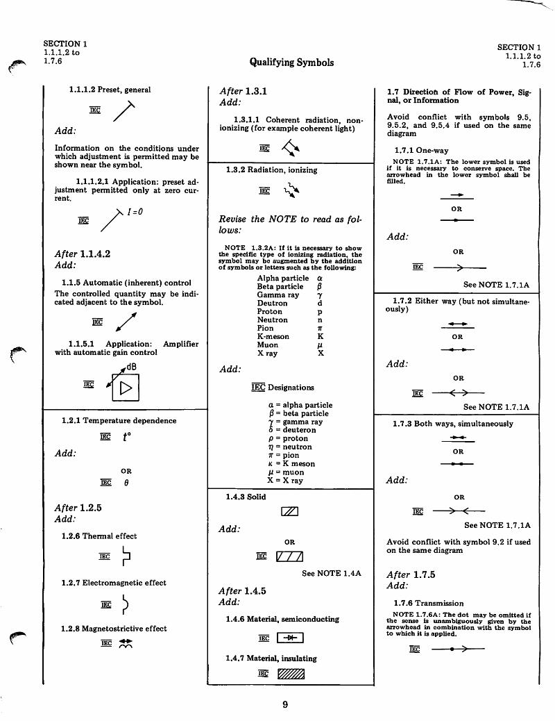
SECTION 1 1.1.1.2 to 1.7.6
1.1.1.2 Preset. general
Add:
Information on the conditions under which adjustment is permitted may be shown near the symbol.
1.1.1.2.1 Application: preset adjustment permitted only at zero current.
After 1.1.4.2 Add:
1.1.5 Automatic (inherent) control The controlled quantity may be indicated adjacent to the symbol.
1.1.5.1 Application: Amplifier with automatic gain control
1.2.1 Temperature dependence
lEe to Add:
OR
lEC 8
After 1.2.5 Add:
1.2.6 Thermal effect
1.2.7 Electromagnetic effect
1.2.8 Magnetostrictive effect
lEC ~
Qualifying Symbols
After 1.3.1 Add:
1.3.1.1 Coherent radiation, nonionizing (for example coherent light)
1.3.2 Radiation, ionizing
Revise the NOTE to read as follows:
NOTE 1.3.2A: If it is necessary to show the specific type of ionizing radiation, the symbol may be augmented by the addition of symbols or letters such as the following:
Add:
Alpha particle Q
Beta particle (3 Gamma ray 'Y Deutron d Proton p Neutron n Pion 7r K-meson K Muon Jl Xray X
IEC Designations
a = alpha particle (3 = beta particle 'Y = gamma ray /) = deuteron p = proton 11 = neutron 7r = pion " = K meson Jl = muon X = X ray
1.4.3 Solid
Add: OR
lEe IZ72l
After 1.4.5 Add:
See NOTE 1.4A
1.4.6 Material, semiconducting
1.4.7 Material, insulating
lEe ~
9
SECTION 1 1.1.1.2 to
1. 7.6
1.7 Directiofl of Flow of Power, Signal, or Infonnation
Avoid conflict with symbols 9.5, 9.5.2. and 9.5.4 if used on the same diagram
1.7.1 One-way NOTE 1.7.1A: The lower symbol is used
if it is necessary to conserve space. The arrowhead in the lower symbol shall be filled.
OR
• Add:
OR
See NOTE 1.7.1A
1.7.2 Either way (but not simultaneously)
OR
• • Add:
OR
lEe ( )
See NOTE 1.7.1A
1.7.3 Both ways, simultaneously
OR
• • Add:
OR
) (
See NOTE 1.7.1A
Avoid conflict with symbol 9.2 if used on the same diagram
After 1.7.5 Add:
1.7.6 Transmission NOTE 1.7.6A: The dot may be omitted if
the sense is unambiguously given by the arrowhead in combination with the symbol to which it is applied.
lEe • )
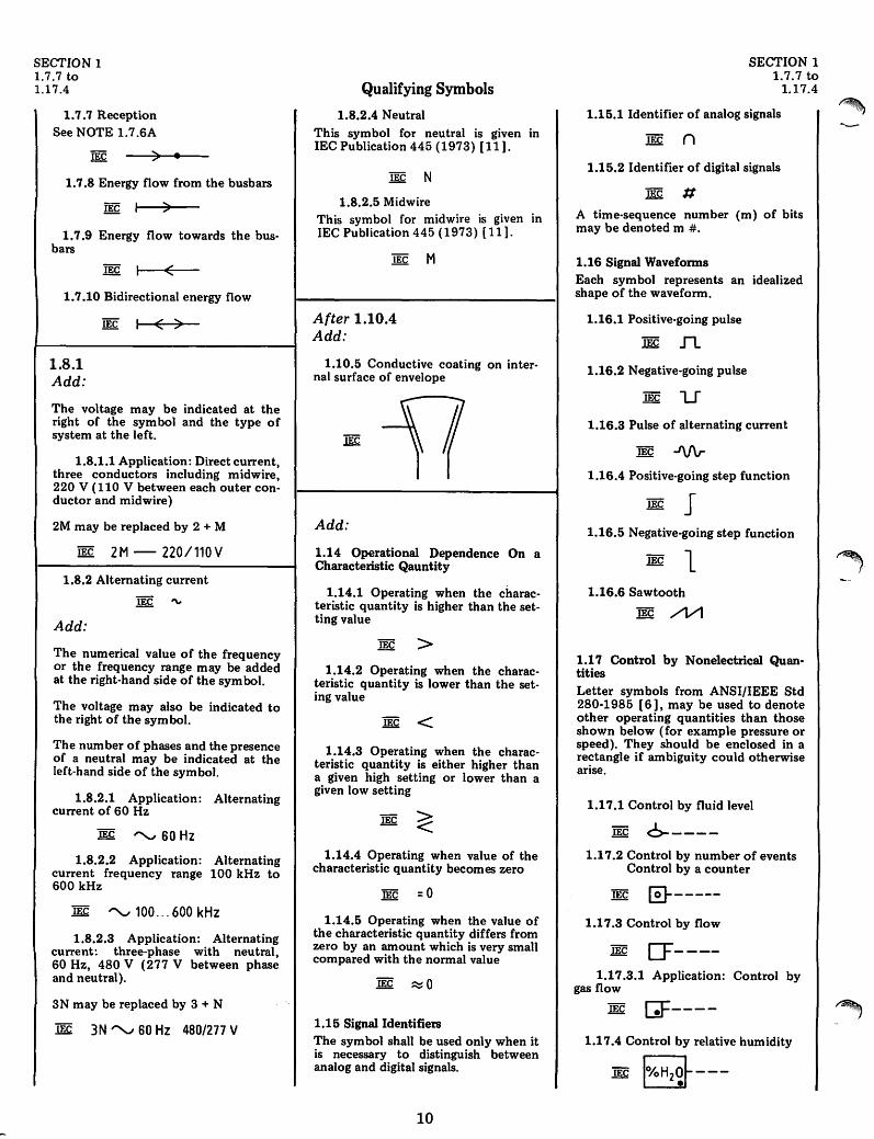
SECTION 1 1.7.7 to 1.17.4
1.7.7 Reception See NOTE 1.7.6A
) . 1.7.8 Energy flow from the busbars
IEC I )
1.7.9 Energy flow towards the busbars
IEC 1 (
1.7.10 Bidirectional energy flow
1.8.1 Add:
IEC I ()
The voltage may be indicated at the right of the symbol and the type of system at the left.
1.8.1.1 Application: Direct current, three conductors including midwire, 220 V (110 V between each outer conductor and midwire)
2M may be replaced by 2 + M
IEC 2M - 220/110V
1.8.2 Alternating current
IEC '"
Add:
The numerical value of the frequency or the frequency range may be added at the right-hand side of the sym hoI.
The voltage may also be indicated to the right of the symbol.
The number of phases and the presence of a neutral may be indicated at the left-hand side of the symbol.
1.8.2.1 Application: Alternating current of 60 Hz
IEC "'- 60 Hz
1.8.2.2 Application: Alternating current frequency range 100 kHz to 600 kHz
IEC "'v 100 ... 600 kHz
1.8.2.3 Application: Alternating current: three-phase with neutral, 60 Hz, 480 V (277 V between phase and neutral).
3N may be replaced by 3 + N
lEe 3N "v 60 Hz 480/277 V
Qualifying Symbols
1.8.2.4 Neutral This symbol for neutral is given in IEC Publication 445 (1973) [11].
IEC N
1.8.2.5 Midwire This symbol for midwire is given in IEC Publication 445 (1973) [111.
IEC M
After 1.10.4 Add:
1.10.5 Conductive coating on internal surface of envelope
Add:
1.14 Operational Dependence On a Characteristic Qauntity
1.14.1 Operating when the characteristic quantity is higher than the setting value
lEe > 1.14.2 Operating when the charac
teristic quantity is lower than the seting value
1.14.3 Operating when the characteristic quantity is either higher than a given high setting or lower than a given low setting
1.14.4 Operating when value of the characteristic quantity becomes zero
lEe = 0
1.14.5 Operating when the value of the characteristic quantity differs from zero by an amount which is very small compared with the normal value
1E£ ~O
1.15 Signal Identifiers The sym bol shall be used only when it is necessary to distinguish between analog and digital signals.
10
SECTION 1 1.7.7 to
1.17.4
1.15.1 Identifier of analog signals
~ n 1.15.2 Identifier of digital signals
lEe II A time-sequence number (m) of bits may be denoted m #.
1.16 Signal Waveforms Each symbol represents an idealized shape of the waveform.
1.16.1 Positive-going pulse
lEe n 1.16.2 Negative-going pulse
lEe U
1.16.3 Pulse of alternating current
lEe .J\J\r 1.16.4 Positive-going step function
lEe J 1.16.5 Negative-going step function
lEe 1 1.16.6 Sawtooth
lEe /V1
1.17 Control by Nonelectrical Quantities Letter symbols from ANSI/IEEE Std 280-1985 [6], may be used to denote other operating quantities than those shown below (for example pressure or speed). They should be enclosed in a rectangle if ambiguity could otherwise arise.
1.17.1 Control by fluid level
lEe 0-----1.17.2 Control by number of events
Control by a counter
IEC @------
1.17.3 Control by flow
lEe IT----1.17.3.1 Application: Control by
gas flow
1E£ [;F----
1.17.4 Control by relative humidity
1EC IO/oH O~---- 2.
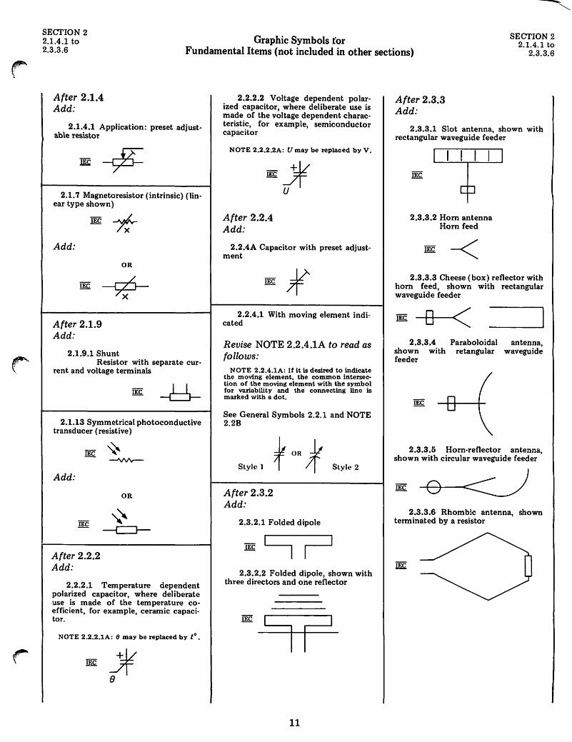
Graphic Symbols for SECI'ION 2 2.1.4.1 to 2.3.3.6 Fundamental Items (not included in other sections)
SECTION 2 2.1.4.1 to
2.3.3.6
After 2.1.4 Add:
2.1.4.1 Application: preset adjust· able resistor
2.1.7 Magnetoresistor (intrinsic) (lin· ear type shown)
lEe +x Add:
After 2.1.9 Add:
2.1.9.1 Shunt
OR
Resistor with separate cur· rent and voltage terminals
lEe ~
2.1.13 Symmetrical photoconductive transducer (resistive)
Add:
After 2.2.2 Add:
OR
2.2.2.1 Temperature dependent polarized capacitor, where deliberate use is made of the temperature co· efficient, for example, ceramic capaci· tor.
NOTE 2.2.2.1A: (J may be replaced by to.
2.2.2.2 Voltage dependent polar· ized capacitor, where deliberate use is made of the voltage dependent charac· teristic, for example, semiconductor capacitor
NOTE 2.2.2.2A: Umay be replaced by V.
-w lEe fi
After 2.2.4 Add:
U
2.2.4A Capacitor with preset adjust· ment
2.2.4.1 With moving element indio cated
Revise NOTE 2.2.4.1A to read as follows:
NOTE 2.2.4.1A: If it is desired to indicate the moving element. the common intersection of the moving element with the symbol for variability and the connecting line is marked with a dot.
See General Symbols 2.2.1 and NOTE 2.2B
Style 1
After 2.3.2 Add:
2.3.2.1 Folded dipole
Style 2
2.3.2.2 Folded dipole, shown with three directors and one reflector
11
After 2.3.3 Add:
2.3.3.1 Slot antenna, shown with rectangular waveguide feeder
2.3.3.2 Hom antenna Hom feed
-< 2.3.3.3 Cheese (box) reflector with
horn feed, shown with rectangular waveguide feeder
--1-4-0 ---«
2.3.3.4 Paraboloidal shown with retangular feeder
antenna, waveguide
2.3.3.5 Horn·reflector antenna, shown with circular waveguide feeder
2.3.3.6 Rhombic antenna, shown terminated by a resistor
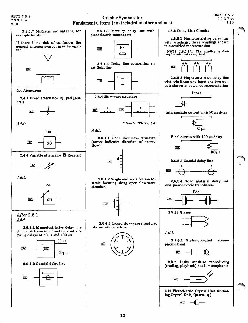
Graphic Symbols for SECTION 2 2.3.3.7 to 2.10 Fundamental Items (not included in other sections)
SECTION 2 2.3.3.7 to
2.10
2.3.3.7 Magnetic rod antenna, for example ferrite.
If there is no risk of confusion, the general antenna symbol may be omitted.
2.4 Attenuator
2.4.1 Fixed attenuator El ; pad (gen-eral)
lEe + Add:
OR
lEe --0-2.4.4 Variable attenuator fI (general)
lEe f Add:
OR
lEe -H-After 2.6.1 Add:
2.6.1.1 Magnetostrictive delay line shown with one input and two outputs giving delays of 50 ps and 100 ps
I~ -1?t: 2.6.1.2 Coaxial delay line
2.6.1.3 Mercury delay line with piezoelectric transducers
2.6.1.4 Delay line comprising an artificial1ine
2.6.4 Slow-wave structure
* lEe ----r-:-l---~ 111""
* See NOTE 2.6.1A
Add:
2.6.4.1 Open slow-wave structure (arrow indicates direction of energy flow)
2.6.4.2 Single electrode for electostatic focusing along open slow-wave structure
2.6.4.3 Closed slow-wave structure, shown with envelope
12
2.6.5 Delay Line Circuits
2.6.5.1 Magnetostrictive delay line with windings; three windings shown in assembled representation
NOTE 2.6.5.1A: The winding symbols may be oriented as required
2.6.5.2 Magnetostrictive delay line with windings; one input and two outputs shown in detached representation
Input
Intermediate output with 50 ps delay
Final output with 100 ps delay
2.6.5.3 Coaxial delay line
e 8 2.6.5.4 Solid material delay line
with piezoelectric transducers
2.9.6* Stereo
--B --Add:
2.9.6.1 Stylus-operated phonic head
stereo-
2.9.7 Light sensitive reproducing (reading, playback) head, monophonic
--_11/ ---1 ~) 2.10 Piezoelectric Crystal Unit (includ· ing Crystal Unit, Quartz !l )
lEe -iOr-
~ ---
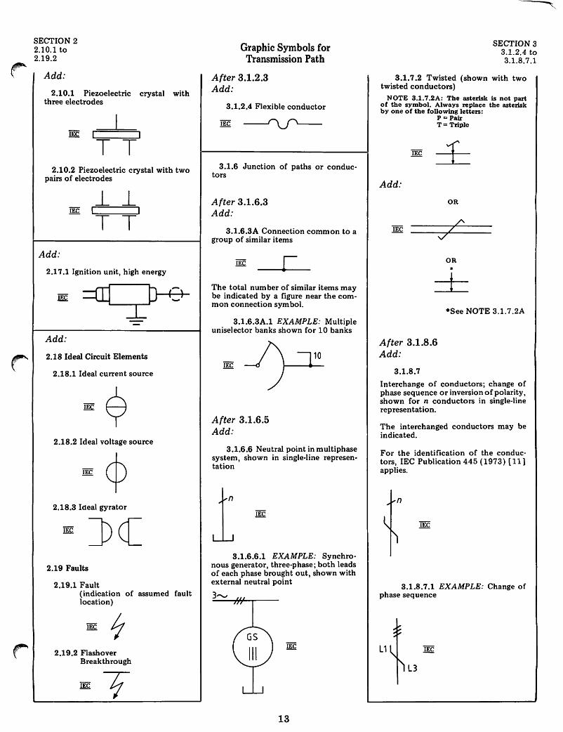
SECTION 2 2.10.1 to 2.19.2
Add:
2.10.1 Piezoelectric crystal with three electrodes
I I
TT 2.10.2 Piezoelectric crystal with two
pairs of electrodes
~~ I I
TT Add:
2.17.1 Ignition unit, high energy
=rrl D , -} lEe -I --
Add:
2.18 Ideal Circuit Elements
2.18.1 Ideal current source
2.18.2 Ideal voltage source
2.18.3 Ideal gyrator
2.19 Faults
2.19.1 Fault (indication of assumed fault location)
2.19.2 Flashover Breakthrough
Graphic Symbols for Transmission Path
After 3.1.2.3 Add:
3.1.2.4 Flexible conductor
3.1.6 Junction of paths or conductors
After 3.1.6.3 Add:
3.1.6.3A Connection common to a group of similar items
The total num ber of similar items may be indicated by a figure near the common connection sym bol.
3.1.6.3A.1 EXAMPLE: Multiple uniselector banks shown for 10 banks
After 3.1.6.5 Add:
3.1.6.6 Neutral point in multiphase system, shown in single-line representation
3.1.6.6.1 EXAMPLE: Synchronous generator three-phase; both leads of each phase brought out, shown with external neutral point
3......., UI
",
GS
III
LU
13
SECTION 3 3.1.2.4 to 3.1.8.7.1
3.1.7.2 Twisted (shown with two twisted conductors)
NOTE 3.1.7.2A: The asterisk is not part of the symbol. Always replace the asterisk by one of the following letters:
P = Pair T= Triple
Add:
After 3.1.B.6 Add:
3.1.8.7
OR
OR
*
*See NOTE 3.1. 7 .2A
Interchange of conductors; change of phase sequence or inversion of polarity, shown for n conductors in single-line representation.
The interchanged conductors may be indicated.
For the identification of the conductors, IEC Publication 445 (1973) [11) applies.
3.1.8.7.1 EXAMPLE: Change of phase sequence
SECTION 3 3.2.6.2 to 3.10.1
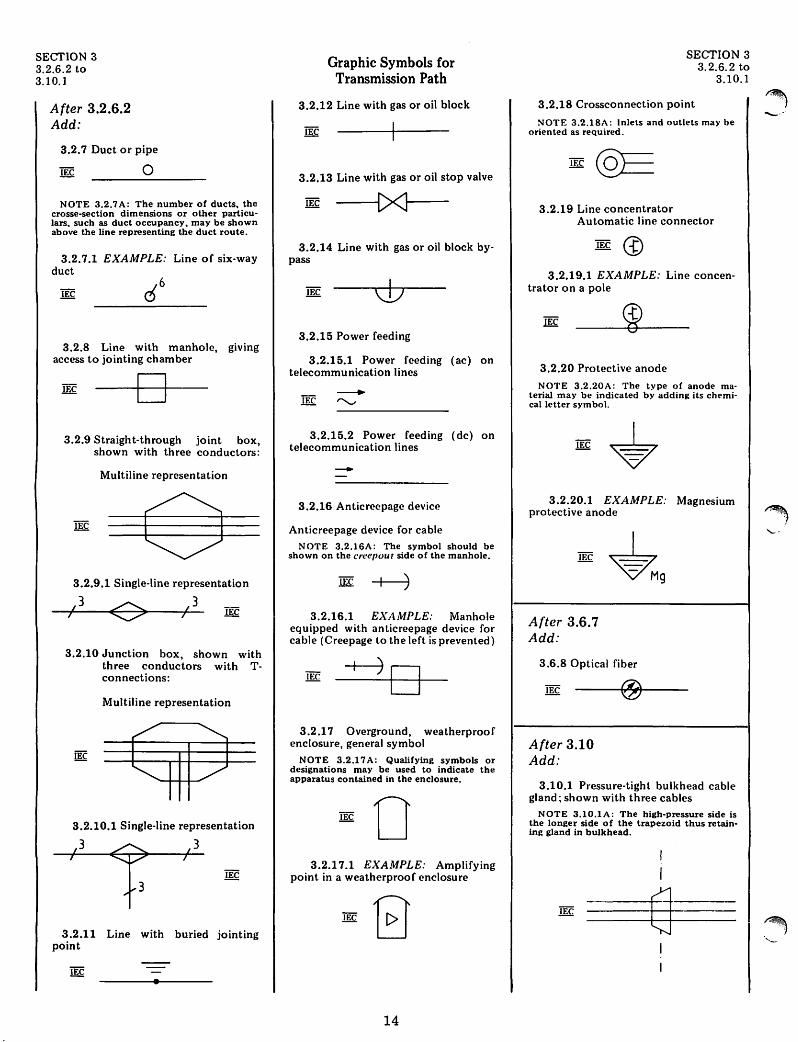
After 3.2.6.2 Add:
3.2.7 Duct or pipe
o
NOTE 3.2.7A: The number of ducts, the crosse-section dimensions or other particulars, such as duct occupancy. may be shown above the line representing the duct route.
3.2.7.1 EXAMPLE: Line of six-way duct
3.2.8 Line with manhole, giving access to jointing chamber
B 3.2.9 Straight-through joint box,
shown with three conductors:
Multiline representation
3.2.10 Junction box, shown with three conductors with Tconnections:
Multiline representation
3.2.10.1 Single-line representation
,3 'T ,3
j f. ) I~
3.2.11 Line with buried jointing point
•
Graphic Symbols for Transmission Path
3.2.12 Line with gas or oil block
3.2.13 Line with gas or oil stop valve
-~[)<]--
3.2.14 Line with gas or oil block bypass
3.2.15 Power feeding
3.2.15.1 Power feeding (ac) on telecommunication lines
3.2.15.2 Power feeding (dc) on telecommunication lines
3.2.16 Anticreepage device
Anticreepage device for cable NOTE 3.2.16A: The symbol should be
shown on the creepuut side of the manhole.
3.2.16.1 EXAMPLE: Manhole equipped with anticreepage device for cable (Creepage to the left is prevented)
3.2.17 Overground, weatherproof enclosure, general symbol
NOTE 3.2.17 A: Qualifying symbols or designations may be used to indicate the apparatus contained in the enclosure.
IF£ 0 3.2.17.1 EXAMPLE: Amplifying
point in a weatherproof enclosure
14
SECTION 3 3.2.6.2 to
3.10.1
3.2.18 Crossconnection point
NOTE 3.2.18A: Inlets and outlets may be oriented as required.
3.2.19 Line concentrator Automatic line connector
3.2.19.1 EXAMPLE: Line concentrator on a pole
3.2.20 Protective anode
NOTE 3.2.20A: The type of anode material may be indicated by adding its chemical letter symbol.
3.2.20.1 EXAMPLE: Magnesium protective anode
After 3.6.7 Add:
3.6.8 Optical fiber
After 3.10 Add:
3.10.1 Pressure-tight bulkhead cable gland; shown with three cables
NOTE a.IO.IA: The high-pressure side is the longer side of the trapezoid thus retaining gland in bulkhead.
I I
G
-.'
Graphic Symbols for SECTION 4 4.1 to 4.3A.1.5 Contacts, Switches, Contactors, and Relays
SECTION 4 4.1 to
4.3A.1.5
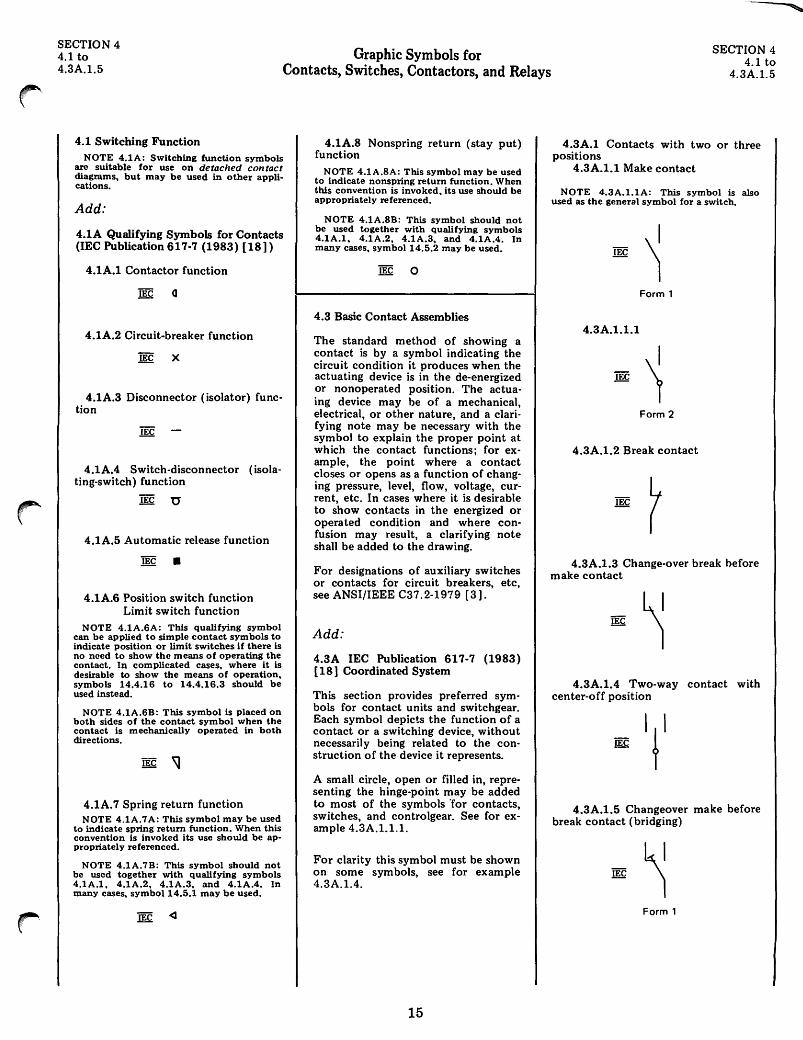
4.1 Switching Function NOTE 4.1A: Switching function symbols
are suitable for use on detached con tact diagrams, but may be used in other applications.
Add:
4.1A Qualifying Symbols for Contacts (lEC Publication 617-7 (1983) [18])
4.lA.l Contactor function
lEe (J
4.lA.2 Circuit-breaker function
lEe X
4.lA.3 Disconnector (isolator) function
4.lA.4 Switch-disconnector (isolating-switch) function
lEe U
4.lA.5 Automatic release function
lEe •
4.lA.6 Position switch function Limit switch function
NOTE 4.1A.6A: This qualifying symbol can be applied to simple contact symbols to indicate position or limit switches if there is no need to show the means of operating the contact. In complicated cases, where it is desirable to show the means of operation, symbols 14.4.16 to 14.4.16.3 should be used instead.
NOTE 4.1A.6B: This symbol is placed on both sides of the contact symbol when the contact is mechanically operated in both directions.
4.lA.7 Spring return function NOTE 4.1A.7A: This symbol may be used
to indicate spring return function. When this convention is invoked its use should be appropriately referenced.
NOTE 4.1A.7B: This symbol should not be used together with qualifying symbols 4.1A.l, 4.1A.2. 4.1A.3. and 4.1A.4. In many cases, symbol 14.5.1 may be used.
4.lA.8 Nonspring return (stay put) function
NOTE 4.1A.8A: This symbol may be used to indicate nonspring return function. When this convention is invoked, its use should be appropriately referenced.
NOTE 4.1A.8B: This symbol should not be used together with qualifying symbols 4.1A.l. 4.1A.2. 4.1A.3. and 4.1A.4. In many cases, symbol 14.5.2 may be used.
lEe 0
4.3 Basic Contact Assemblies
The standard method of showing a contact is by a symbol indicating the circuit condition it produces when the actuating device is in the de-energized or nonoperated position. The actuaing device may be of a mechanical, electrical, or other nature, and a clarifying note may be necessary with the symbol to explain the proper point at which the contact functions; for ex· ample, the point where a contact closes or opens as a function of changing pressure, level, flow, voltage, current, etc. In cases where it is desirable to show contacts in the energized or operated condition and where confusion may result, a clarifying note shall be added to the drawing.
For designations of auxiliary switches or contacts for circuit breakers, etc, see ANSI/IEEE C37.2-1979 [3].
Add:
4.3A IEC Publication 617-7 (1983) [18] Coordinated System
This section provides preferred sym· boIs for contact units and switchgear. Each symbol depicts the function of a contact or a switching device, without necessarily being related to the construction of the device it represents.
A small circle, open or filled in, representing the hinge·point may be added to most of the symbols 'for contacts, switches, and controlgear. See for example 4.3A.1.1.1.
For clarity this symbol must be shown on some symbols, see for example 4.3A.1.4.
15
4.3A.l Contacts with two or three positions
4.3A.l.1 Make contact
NOTE 4.3A.1.1A: This symbol is also used as the general symbol for a switch.
Form 1
4.3A.l.LI
Form 2
4.3A.1.2 Break contact
4.3A.L3 Change-over break before make contact
4.3A.l.4 Two-way contact with center-off position
4.3A.l.5 Changeover make before break contact (bridging)
Form 1
Graphic Symbols for SECTION 4 4.3A.1.5.1 to 4.3A.5.4 Contacts, Switches, Contactors, and Relays
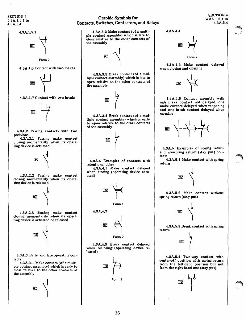
4.3A.l.5.l
Form 2
4.3A.l.6 Contact with two makes
4.3A.1. 7 Contact with two breaks
4.3A.2 Passing contacts with two positions
4.3A.2.l Passing make contact closing momentarily when its opera· ting device is actuated
4.3A.2.2 Passing make contact closing momentarily when its operating device is released
4.3A.2.3 Passing make contact closing momentarily when its operating device is actuated or released
4.3A.3 Early and late operating contacts
4.3A.3.l Make contact (of a multiple contact assembly) which is early to close relative to the other contacts of the assembly
4.3A.3.2 Make contact (of a multiple contact assembly) which is late to close relative to the other contacts of the assembly
4.3A.3.S Break contact (of a multiple contact assembly) which is late to open relative to the other contacts of the assembly
4.3A.3.4 Break contact (of a multiple contact assembly) which is early to open relative to the other contacts of the assembly
4.3A.4 Examples of contacts with intentional delay
4.3A.4.l Make contact delayed when closing (operating device actuated)
Form 1
4.3A.4.2
Form 2
4.3A.4.3 Break contact delayed when reclosing' (operating device released)
Form 1
16
4.3A.4.4
Form 2
SECTION 4 4.3A.1.5.l to
4.3A.5.4
4.3A.4.5 Make contact delayed when closing and opening
4.3A.4.6 Contact assembly with one make contact not delayed, one make contact delayed when reopening and one break contact delayed when opening
I r !t.t ~c ~--r-r
4.3A.5 Examples of spring return and nonspring return (stay put) contacts
4.3A.5.l Make contact with spring return
4.3A.5.2 Make contact without spring return (stay put)
4.3A.5.S Break contact with spring return
4.3A.5.4 Two-way contact with center-off position with spring return from the left-hand position but not from the right-hand one (stay put)
SECI'ION 4 4.3B to 4.29.1
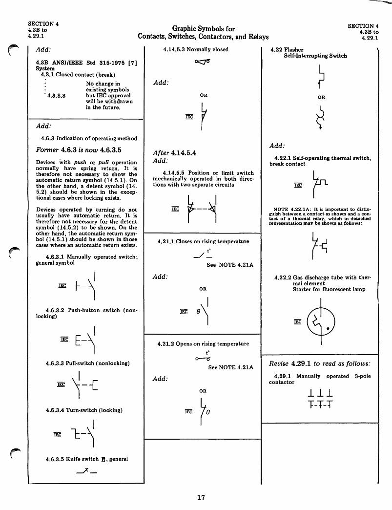
Add:
4.3B ANSllIEEE Std 315-1975 [7] System
4.3.1 Closed contact (break)
. 4.3.8.3
Add:
No change in existing symbols but IEC approval will be withdrawn in the future.
4.6.3 Indication of operating method
Former 4.6.3 is now 4.6.3.5
Devices with push or pull operation normally have spring return. It is therefore not necessary to show the automatic return symbol (14.5.1). On the other hand, a detent symbol (14. 5.2) should be shown in the exceptional cases where locking exists.
Devices operated by turning do not usually have automatic return. It is therefore not necessary for the detent symbol (14.5.2) to be shown. On the other hand, the automatic return symbol (14.5.1) should be shown in those cases where an automatic return exists.
4.6.3.1 Manually operated switch; general sym bol
4.6.3.2 Push-button switch (nonlocking)
4.6.3.3 Pull-switch (nonlocking)
4.6.3.4 Turn-switch (locking)
4.6.3.5 Knife switch fI, general
-p_
Graphic Symbols for Contacts, Switches, Contactors, and Relays
4.14.5.3 Normally closed
Add:
After 4.14.5.4 Add:
OR
4.14.5.5 Position or limit switch mechanically operated in both directions with two separate circuits
4.21.1 Closes on rising temperature
to J_
See NOTE 4.21A
Add:
OR
4.21.2 Opens on rising temperature to
o---tr
See NOTE 4.21A
Add:
OR
17
4.22 Flasher Self-Interrupting Switch
OR
Add:
SECTION 4 4.3B to 4.29.1
4.22.1 Self-operating thermal switch, break contact
NOTE 4.22.1A: It is important to distinguish between a contact as shown and a contact of a thermal relay. which in detached representation may be shown as follows:
4.22.2 Gas discharge tube with thermal element Starter for fluorescent lamp
•
Revise 4.29.1 to read as follows:
4.29.1 Manually operated 3-pole contactor
-L-L1-T-T-T
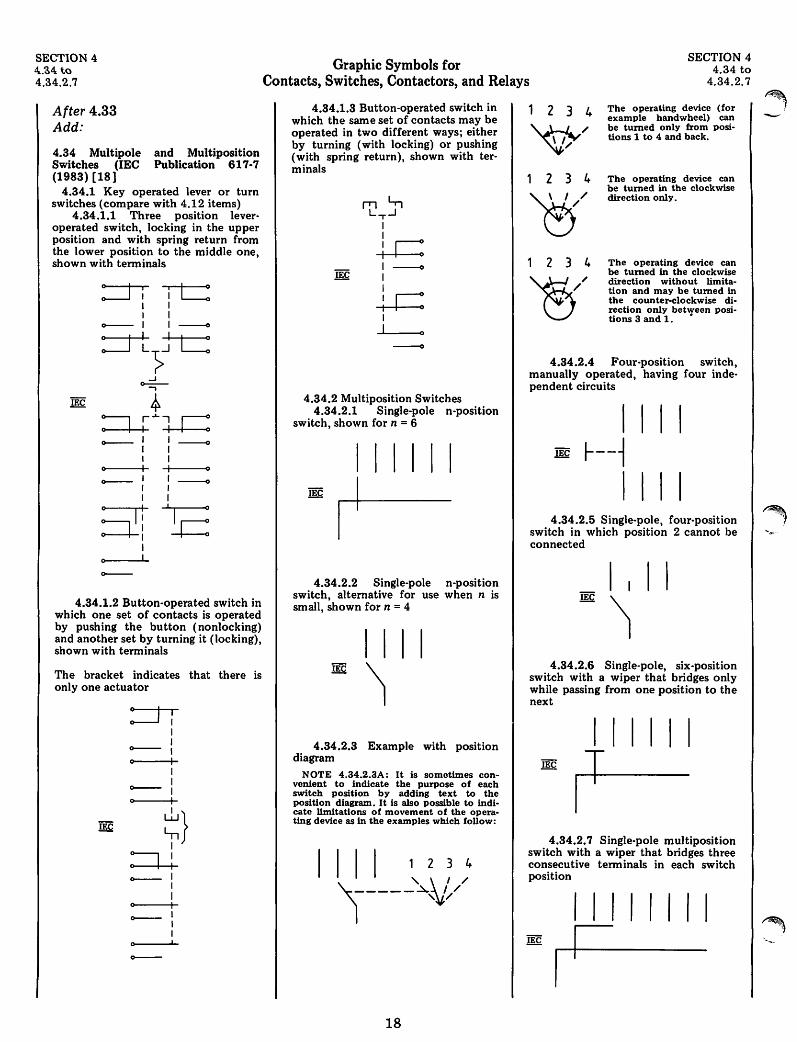
SECTION 4 4..?>4. to 4.34.2.7
After 4.33 Add:
4.34 Multipole Switches (lEe (1983) [18]
and Multiposition Publication 617-7
4.34.1 Key operated lever or turn switches (compare with 4.12 items)
4.34.1.1 Three position leveroperated switch, locking in the upper position and with spring return from the lower position to the middle one, shown with terminals
:=J i L: I 1
~ 1-
:=J L}J L: ...J ~ -,
lEe ~ :-l j.L j r=: ~I I-
I I I I
0----+-1 1 0
~I I-I I I I
~i't 1 I
4.34.1.2 Button-operated switch in which one set of contacts is operated by pushing the button (nonlocking) and another set by turning it (locking), shown with terminals
The bracket indicates that there is only one actuator
I 1
~I
I
~I I I I
~
Graphic Symbols for Contacts, Switches, Contactors, and Relays
SECTION 4 4.34 to
4.34.2.7
4.34.1.3 Button-operated switch in which the same set of contacts may be operated in two different ways; either by turning (with locking) or pushing (with spring return), shown with terminals
~Jt ,. I I I r=: I 1 -lEe 1 1 I r=: I I I
~
4.34.2 Multiposition Switches 4.34.2.1 Single-pole n-position
switch, shown for n = 6
I I I I I I
4.34.2.2 Single-pole n-position switch, alternative for use when n is small, shown for n = 4
I I I I ~
4.34.2.3 Example with position diagram
NOTE 4.34.2.3A: It is sometimes convenient to indicate the purpose of each switch position by adding text to the position diagram. It is also possible to indicate limitations of movement of the operating device as in the examples which follow:
18
234
~/
234
r!)/ 234
The operating device (for example handwheel) can be turned only from positions 1 to 4 and back.
The operating device can be turned in the clockwise direction only.
The operating device can be turned in the clockwise direction without limitation and may be tumed in the counter-clockwise direction only between posi-tions 3 and 1. •
4.34.2.4 Four-position switch, manually operated, having four independent circuits
I I I I lEe ~--1
I I I I 4.34_2.5 Single-pole, four-position
switch in which position 2 cannot be connected
I
~ I I
4.34.2.6 Single-pole, six-position switch with a wiper that bridges only while passing from one position to the next
I I I I I I
4.34.2.7 Single-pole multiposition switch with a wiper that bridges three consecutive terminals in each switch position
I I I I I I I I Ir=
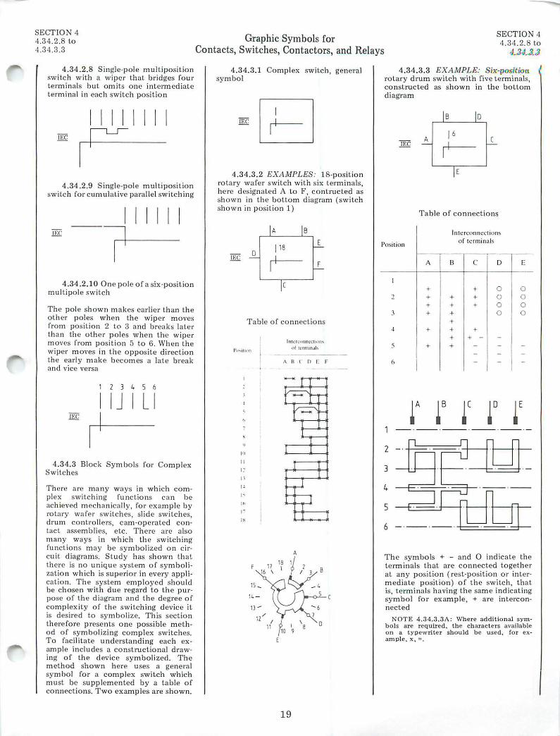
SECT ION 4 4.34.2.8 to 4 .34.3 .3
4.34.2.8 Single-pole Inui t iposii ioll switch with a wiper t hat bridges four terminals but omits one intermed iate terminal in each switch position
I I I I I I I I
I~ 4 .34.2.9 Single-pole multiposilion
switch for CUIll ulative pa rallel switch ing
I I I I I I
7 4.34.2.10 One pole of a six-pos ition
mul l ipole swi tch
The pole shown makes earlier than the other poles when the wiper moves from posit ion 2 to 3 and brea ks later than the oiher poles when the wiper moves from position 5 to 6. When lhe wiper moves in the opposite direct ion the early make becomes a late break and vice versa
1 1 4 \ 6
IIJILI
r-4.34.3 Block Symbols for Complex
Swi tches
There are many ways in which complex swi tching func t ions can be ac hieved mechanically , for ex ample by ro tary wafer switches, slide switches, drum controllers , cam·operated contac t assem b lies, etc. There a re also many ways in which th e switching [unct.ions m ay be symbolized on c ircuit diagrams. Study has show n that t.here is no uniqu e system of symbolization which is superior in every applica tion. The sys tem employed should be chosen with due regard to the purpose o f the diagram a nd t he de gree of complexity of the switching device it is des ire d to symbolize. This section therefore presents o ne poss ible method of symbolizing complex swi tches. To faci litate u nderstanding each example includes a constructiona l drawing of the device symbol ized. The method shown here uses a general symbol for a complex switch which must be supplemented by a t a ble of connections. Two examples are shown.
Graphic Sym boIs for Contacts, Switches, Contactors, and Relays
SECT ION 4 4.34.2.8 to
4.34.33
4 .34.3.1 Complex switch, general symbol
lEe !!III LCJ
4.34.3.2 EXAMPLES: IS-posit ion rotary wafer switch with s ix terminals, here des ignated A to £", contructed as shown in the boltom diagram (switch shown in pos ition 1)
lEe
'" " " " ,. " ". "
"
1 18 E
0
II (
Table of connectio ns
17 18 16 \ \
Inl<'.<:<,,,nC ... l,,,,,, ,\I 1l"r"" n~l,
,\ n (" [) I: F
-r- r---
r= f-r-
Jr.=.'"
r
f-;=I
19
4 .34 .3.3 EXAMPLE: S ix-positio n rotary drum switch with fiv e t erminals, constructed as shown in the bottom diagram
o
A
E
Table of connections
Int e rconnections
Position of terminals
A B C D [
1 + + 0 0 , + + + 0 0 + + + 0 0
3 + + 0 0 + , + + + + + - -
5 + + - - -- - -
" - - -
2
3
4 ~.-.-._-_.
5
6
The symbols + - and 0 indicate the terminals t hat are connected together at any position (rest-position or intermediate position) of the switch, that is, termina ls having the same indicating symbol for example, + are interconnected
NOTE 4.34.3.3A: Where additional symbols are required, the characte rs available o n a typewrite r should be used. for example, x, = .
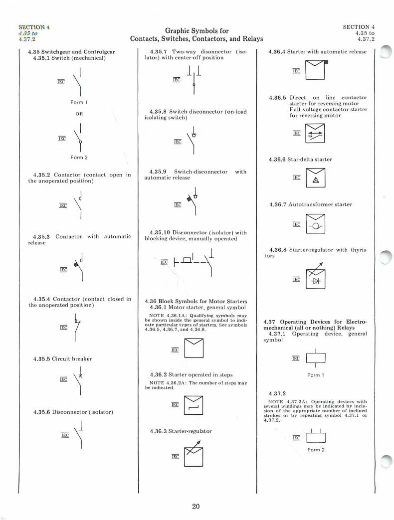
Graphic Symbols for SECTION 4 4.35 to 4.37.2 Contacts, Switches, Contactors, and Relays
4.35 Switchgear and Controlgear 4.35.1 Sw itch (m echanical)
Form 1
OR
lEe ) Form 2
4.35.2 Contactor (con tact open in the unoperated position)
4.35.3 Conlactor with automatic release
4.35.4 Conlaclor (co ntact closed in the unoperalcd position)
4.35 .5 Circuit breaker
".35.6 Disconn ector (iso lator)
4.35.7 Two-way disonncctor (isolalor) with center-orr positio n
4.35.8 Switch-d isconnector (on-load isolating switch)
4.35.9 Sw ilch·disco nneclor with automatic release
4.35 .10 Oisconncclor (isolator) with blocking device, manually operated
4.36 Block Symbols for Molor Starters 4 .36.1 Motor starler, general sy mbol
NOTE 4.36.1A : Qualir)'in~ sy mbols may be shown in sid e the Reneral sy mbol t o inclicalC partic ular types of starters. See sy mbols 4.36.5,4 .36.7, and 4 .:16.8.
4.36.2 Starter operated in steps
NOT E '1.36.2A : The number of ste ps may b e indicated.
4_36.3 Starter-regulator
20
SECTIO N 4 4.35 to 4.37.2
4.36.4 Starter with automatic release
4 .36.5 Direct on iine co ntactor starter for reversi ng motor Full voltage contactor starter for reversing m otor
4 .36.6 S tar-de lta starter
4.36.7 Autotransfonner sta rter
4.36.8 Starter-regulator with thyristors
4.37 Operating Devices for Electromechanical (all or nothing) Relays
4_37.1 Ope rating d evice, general symbol
Form 1
4.37.2
NOTE '1.37.2" : OJleratin~ devices with seve ral windin~s 1ll:I Y b e ind icated by inclusion of the ilppropriate number o f inclined s trok es or by repea tin~ symbo l 4.3 7 .1 o r 4.37 .2.
Form 2
Graphic Symbols for SECTION 4 4.37.3 to 4.37.20 Contacts, Switches, Contactors, and Relays
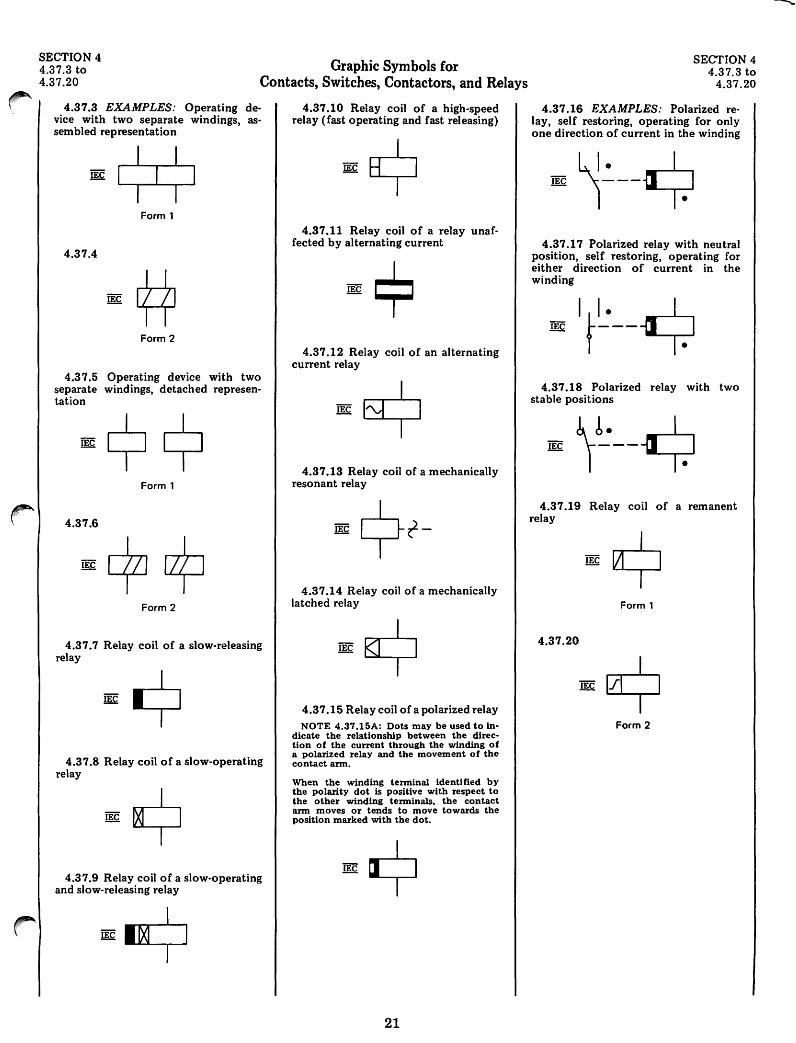
4.37.3 EXAMPLES: Operating device with two separate windings, assembled representation
Form 1
4.37.4
Form 2
4.37.5 Operating device with two separate windings, detached representation
Form 1
4.37.6
Form 2
4.37.7 Relay coil of a slow-releasing relay
4.37.8 Relay coil of a slow-operating relay
4.37.9 Relay coil of a slow-operating and slow-releasing relay
4.37.10 Relay coil of a high-speed relay (fast operating and fast releasing)
4.37.11 Relay coil of a relay unaffected by alternating current
4.37.12 Relay coil of an alternating current relay
4.37.13 Relay coil of a mechanically resonant relay
4.37.14 Relay coil of a mechanically latched relay
4.37.15 Relay coil of a polarized relay NOTE 4.37.15A: Dots may be used to in
dicate the relationship between the direction of the current through the winding of a polarized relay and the movement of the contact arm.
When the winding terminal identified by the polarity dot is positive with respect to the other winding terminals, the contact arm moves or tends to move towards the position marked with the dot.
21
SECTION 4 4.37.3 to
4.37.20
4.37.16 EXAMPLES: Polarized relay, self restoring, operating for only one direction of current in the winding
4.37.17 Polarized relay with neutral position, self restoring, operating for either direction of current in the winding
4.37.18 Polarized relay with two stable positions
4.37.19 Relay coil of a remanent relay
IEC 9 Form 1
4.37.20
IEC ~ Form 2
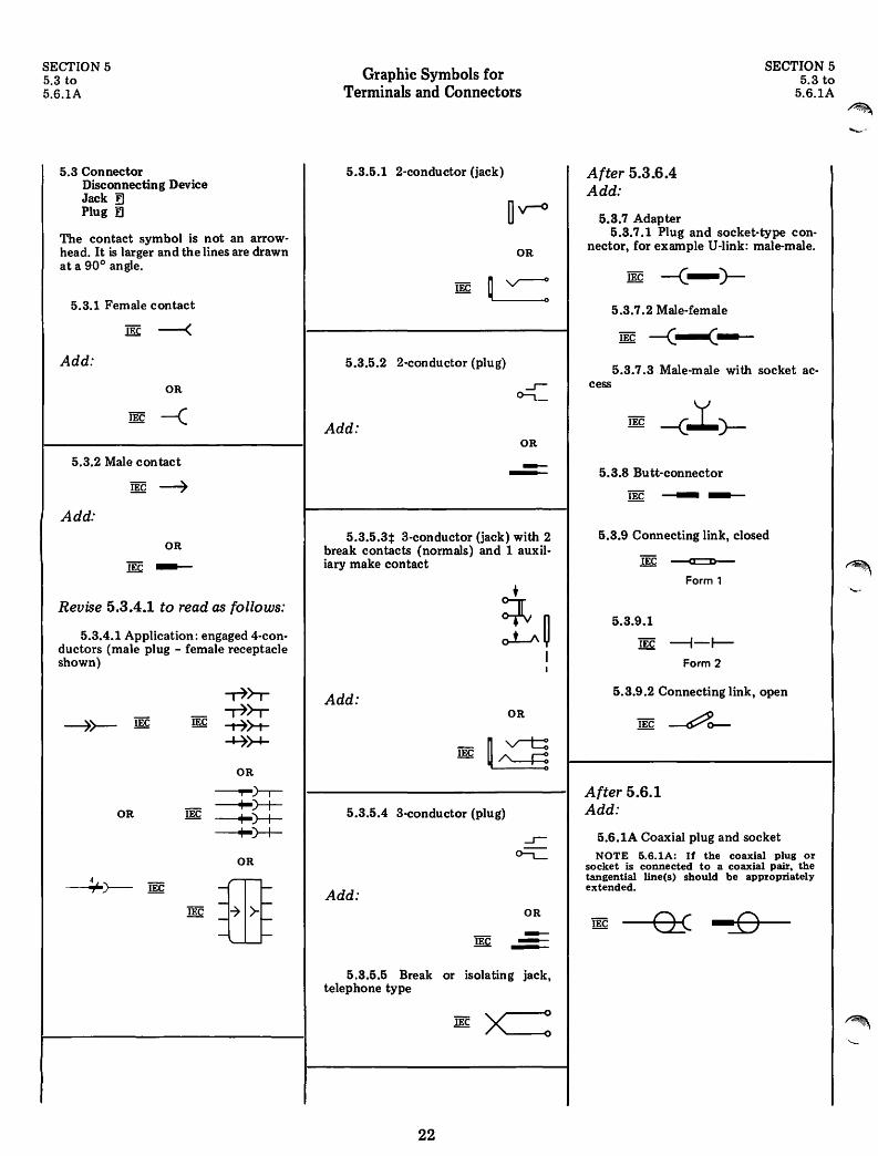
SECTION 5 5.3 to 5.6.1A
5.3 Connector Disconnecting Device Jack !J Plug II
The contact symbol is not an arrowhead. It is larger and the lines are drawn at a 90° angie.
5.3.1 Female contact
--< Add:
OR
5.3.2 Male contact
lEe ~
Add:
OR
Revise 5.3.4.1 to read as follows:
5.3.4.1 Application: engaged 4-conductors (male plug - female receptacle shown)
~>r
lEe ~>r -t7>-r ..+7)-1-
OR
~>--r-
OR lEe -----t-)-t------t-)-t------t-)_+_
OR
lEe fa
Graphic Symbols for Terminals and Connectors
5.3.5.1 2-conductor (jack)
OR
5.3.5.2 2-conductor (plug)
Add: OR
--5.3.5.3+ 3-conductor (jack) with 2
break contacts (normals) and 1 auxiliary make contact
Add: OR
5.3.5.4 3-conductor (plug)
Add: OR
---5.3.5.5 Break or isolating jack,
telephone type
22
After 5.3.6.4 Add:
5.3.7 Adapter
SECTION 5 5.3 to
S.6.lA
5.3.7.1 Plug and socket-type connector, for example U-link: male-male.
5.3.7.2 Male-female
lEe -{--<--5.3.7.3 Male-male with socket ac-
cess
5.3.8 Butt-connector
5.3.9 Connecting link, closed
lEe ~
Form 1
5.3.9.1
lEe ---;-r Form 2
5.3.9.2 Connecting link, open
lEe ~o--
After 5.6.1 Add:
5.6.1A Coaxial plug and socket NOTE o.6.1A: If the coaxial plug or
socket is connected to a coaxial pair. the tangential line(s) should be appropriately extended.
SECTION 6 6.1.2 to 6.4.7
6.1.2 Magnetic core of inductor or transformer
Not to be used unless it is necessary to identify a magnetic core.
Add:
OR
Revise 6.2.1 to read as follows:
6.2.1 General NOTE 6.2.1A: This symbol is deprecated
and should not be used on new schematics.
See NOTE 6.2.1A
Add:
6.2.1A Choke Reactor
See NOTE 6.4.1A
6.2.2 Magnetic-core inductor Telephone loading coil
If necessary to show a magnetic core.
Add:
OR
6.2.2.1 Inductor with gap in magnetic core
Add: 6.2.4.1 Inductor with moving con
tact, variable in steps
Graphic Symbols for Transformers, Inductors, and Windings
After 6.2.5 Add:
6.2.SA Variometer
6.2.9 See new 11.3.3
After 6.2.9 Add:
6.2.10 Coaxial choke with magnetic core
6.2.11 Ferrite bead, shown on a conductor
lEe Fl See also 15.18.1
Revise NOTE 6.4.1A to read as follows:
NOTE 6.4.1A: This symbol is the preferred single-line symbol in IEC Publication 617-6 (1983) [17]. It should be used on schematics for equipments having international usage, especially when the equipment will be marked using this symbol (in accordance with IEC Publication 417 (1973) [10].
6.4.2.3 Application: transformer with magnetic core shown and with an electrostatic shield between windings. The shield is shown connected to the frame.
Add:
6.4.2.3A Single-phase transformer with two windings and screen.
23
LJ II
SECTION 6 6.1.2 to
6.4.7
Revise 6.4.4 to read as follows:
6.4.4 One winding with adjustable inductance
OR
See NOTE 6.4.4A
See NOTE 6.4.1A
NOTE 6.4.4A: The former right-hand e symbol has been deleted. It is no longer recommended for use on complete diagrams.
6.4.6 Adjustable mutual inductor; constant-current transformer
Add: OR
6.4.7 With taps, I-phase
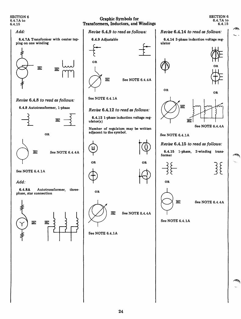
SECTION 6 6.4.7A to 6.4.15
Add:
6.4.7 A Transformer with center tapping on one winding
LJ IEC m
Revise 6.4.8 to read as follows:
6.4.8 Autotransformer, I-phase
--L OR
See NOTE 6.4.4A
See NOTE 6.4.1A
Add:
6.4.8A Autotransformer, three· phase, star connection
Graphic Symbols for Transformers, Inductors, and Windings
Revise 6.4.9 to read as follows:
6.4.9 Adjustable
OR
IEC See NOTE 6.4.4A
See NOTE 6.4.1A
Revise 6.4.12 to read as follows:
6.4.12 I-phase induction voltage regulator(s)
Number of regulators may be written adjacent to the symbol.
OR OR
OR
See NOTE 6.4.4A
See NOTE 6.4.1A
24
SECTION 6 6.4.7A to
6.4.15
Revise 6.4.14 to read as follows:
6.4.14 3-phase induction voltage regulator
OR
OR OR
See NOTE 6.4.4A
See NOTE 6.4.1A
Revise 6.4.15 to read as follows:
6.4.15 I-phase, 2-winding transformer
OR
IEC See NOTE 6.4.4A
See NOTE 6.4.1A
--
.'0-
(~ \
SECTION 6 6.4.15.1 to 6.4.17
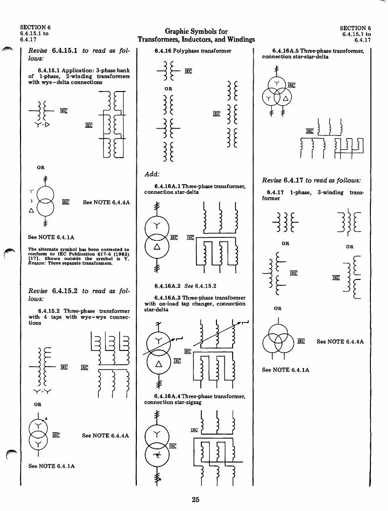
Revise 6.4.15.1 to read as follows:
6.4.15.1 Application: 3-phase bank of I-phase, 2-winding transformers with wye-delta connections
OR
lEe See NOTE 6.4.4A
See NOTE 6.4.1A
The altemate symbol has been corrected to conform to lEe Publication 617-6 (1983) [17] . Shown outside the symbol is Y. Reason: Three separate transformers.
Revise 6.4.15.2 to read as follows:
6.4.15.2 Three-phase transformer with 4 taps with wye-wye connections
y-y
OR
See NOTE 6.4.4A
See NOTE 6.4.1A
Graphic Symbols for Transformers, Inductors, and Windings
6.4.16 Polyphase transformer
OR
Add:
6.4.16A.l Three-phase transformer, connection star-delta
6.4.16A.2 See 6.4.15.2
6.4.16A.3 Three-phase transformer with on-load tap changer, connection star-delta
6.4.16A.4 Three-phase transformer, connection star-zigzag
25
SECTION 6 6.4.15.1 to
6.4.17
6.4.16A.5 Three-phase transformer, connection star-star-delta
Revise 6.4.17 to read as follows:
6.4.17 I-phase, former
OR
OR
See NOTE 6.4.1A
3-winding trans-
OR
-][ ~ [
See NOTE 6.4.4A
SECTION 6 6.4.18 to 6.6.2
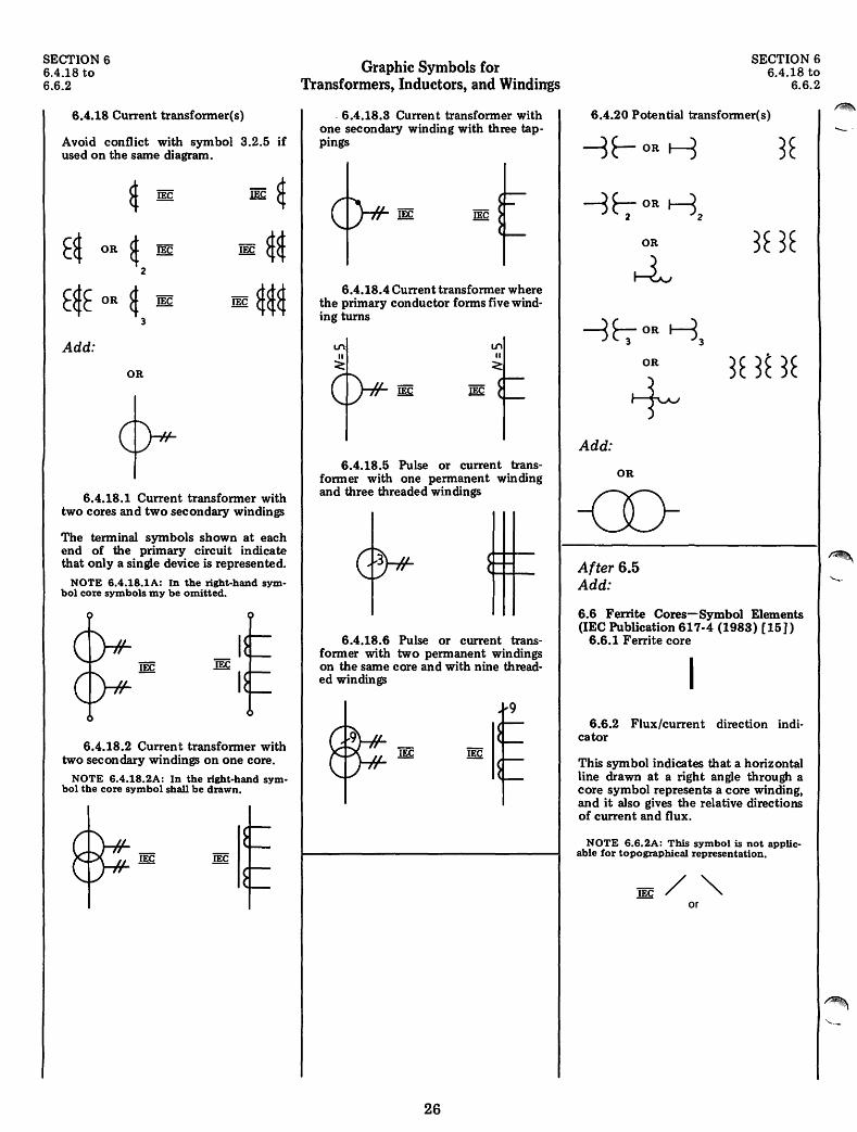
6.4.18 Current transformer(s)
Avoid conflict with symbol 3.2.5 if used on the same diagram.
~ lEe lEe ~
t~ OR ~ ~ lEe ~~ 2
t~t OR ~ lEe lEe ~~~ 3
Add:
OR
6.4.18.1 Current transformer with two cores and two secondary windings
The terminal symbols shown at each end of the primary circuit indicate that only a single device is represented.
NOTE 6.4.18.1A: In the right-hand symbol core symbols my be omitted.
6.4.18.2 Current transformer with two secondary windings on one core.
NOTE 6.4.18.2A: In the right-hand symbol the core symbol shall be drawn.
Graphic Symbols for Transformers, Inductors, and Windings
.6.4.18.3 Current transformer with one secondary winding with three tappings
6.4.18.4 Current transformer where the primary conductor forms five winding turns
U"\ II
<:: U"\ II
<:
6.4.18.5 Pulse or current transformer with one permanent winding and three threaded windings
~--
6.4.18.6 Pulse or current transformer with two permanent windings on the same core and with nine threaded windings
26
SECTION 6 6.4.18 to
6.6.2
6.4.20 Potential transformer(s)
-3 t-- OR r---3 3t
-3 t-:- OR r---3 2 2
OR
-3 f-:- OR r---3 3 3
OR
+ Add:
OR
-co-After 6.5 Add:
3t 3t
3t 3t 3t
6.6 Ferrite Cores-Symbol Elements (lEe Publication 617·4 (1983) [15])
6.6.1 Ferrite core
6.6.2 Flux/current direction indicator
This symbol indicates that a horizontal line drawn at a right angle through a core symbol represents a core winding, and it also gives the relative directions of current and flux.
NOTE 6.6.2A: This symbol is not applicable for topographical representation.
or
',..
r
r
SECTION 6 6.6.3 to 6.8.2
6.6.3 Ferrite core with one winding
-+ The oblique line may be regarded as a reflector that relates the directions of current and flux as shown below.
t Flux
cur~-+ OR
T~enl Flux
For drawing convenience, lines repre· senting conductors are often shown crossing core symbols even though there is no winding on the magnetic circuit. Except in topographical repre· sentation the use of the oblique stroke is mandatory in all cases where a line through the core symbol represents a winding.
EXAMPLE:
* Conductor crossing the core symbol ** Winding on the core
6.7 Ferrite Cores (lEC Publication 617·4 (1983) [15])
6.7.1 Ferrite core with five windings NOTE 6.7.1A: Information on the direc
tion of current. its relative amplitude and the logic conditions imposed by the state of the magnetic remanence may be added.
6.7.2 Ferrite core with one winding ofm turns
lEe ~ -~m
Graphic Symbols for Transformers, Inductors, and Windings
6.8 Magnetic Storage Matrices (Topographical Representation)
6.8.1 Ferrite core matrix with x and y windings and a readout winding. The symbol of a ferrite core, 6.6.1, is shown at 450 to the horizontal.
6.8.2 Matrix arrangement comprising thin sheet magnetic stores, located between thin sheet wiring layers.
27
SECTION 6 6.6.3 to
6.8.2
SECTION 7 7.1.1.1 to 7.1.10.3
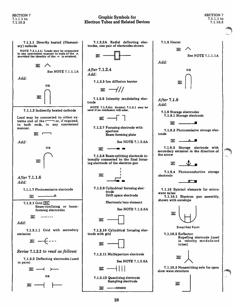
7.1.1.1 Directly heated (filamentary) cathode
NOTE 7.1.1.1A: Leads may be connected in any convenient manner to ends of the A. provided the identity of the A is retained.
.!E&A See NOTE 7.1.1.1A
Add:
OR
7.1.1.2 Indirectly heated cathode
Lead may be connected to either extreme end of the .--. or, if required, to both ends, in any convenient manner.
Add: OR
After 7.1.1.6 Add:
7.1.1. 7 Photoemissive electrode
A
7.1.2.1 Grid lEe
Add:
Beam-confining or beamforming electrodes
7.1.2.1.1 Grid with secondary emission
lEe --E ---Revise 7.1.2.2 to read as follows:
7.1.2.2 Deflecting electrodes (used in pairs)
lEe --< >--OR
Graphic Symbols for Electron Tubes and Related Devices
7.1.2.2A Radial deflecting electrodes, one pair of electrodes shown
After 7.1.2.4 Add:
7.1.2.5 Ion diffusion barrier
~ ---/11 7.1.2.6 Intensity modulating elec
trode NOTE 7.1.2.6A: Symbol 7.1.2.1 may be
used if no confusion will arise.
lEe --r l 7.1.2.7 Focusing electrode with
aperture Beam-forming plate
See NOTE 7.1.2.6A
lEe - -
7.1.2.8 Beam-splittfng electrode internally connected to the final focusing electrode of the electron gun
I I I
- .... ~--7.1.2.9 Cylindrical focusing elec
trode Drift space electrode
Electronic lens elemen t
See NOTE 7.1.2.6A
7.1.2.10 Cylindrical focusing electrode with grid
7.1.2.11 Multiaperture electrode
See NOTE 7.1.2.6A
lEe -illl 7.1.2.12 Quantizing electrode
Sampling electrode
lEe --00000
28
7.1.5 Heater
IEC A
SECTION 7 7.1.1.1 to
7.1.10.3
See NOTE 7.1.1.1A
Add:
After 7.1.8 Add:
OR
7.1.9 Storage electrodes 7.1.9.1 Storage electrode
• 7.1.9.2 Photo emissive storage elec
trode
A •
7.1.9.3 Storage electrode with secondary emission in the direction of the arrow
• 7.1.9.4 Photoconductive storage
electrode
7.1.10 Symbol elements for microwave tubes
7.1.10.1 Electron gun assembly, shown with envelope
Simplified Form
7.1.10.2 Reflector Repelling electrode (used in velocity modulated tubes)
7.1.10.3 Nonemitting sole for open slow-wave structure
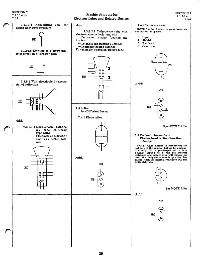
SECTION 7 7.1.10.4 to 7.5A
7.1.10.4 Nonemitting sole for closed slow-wave structure
7.1.10.5 Emitting sole (arrow indicates direction of electron flow)
~J 7.3.6.1 With electric-field (electro
static) deflection
Add:
7.3.6.1.1 Double-beam cathoderay tube, split-beam type with: Electrostatic deflection Indirectly heated cathode
Graphic Symbols for Electron Tubes and Related Devices
Add:
7.3.6.2.3 Cathode-ray tube with electromagnetic deviation, with:
- Permanent magnet focusing and ion trap
- Intensity modulating electrode - Indirectly heated cathode
For example, television picture tube
7.4 Solion Ion-Diffusion Device
7.4.1 Diode solion
Add:
OR
29
7.4.2 Tetrode solion
SECTION 7 7.1.10.4 to
7.5A
NOTE 7 A.2A: Letters in parentheses are not part of the sym bo1.
I Input S Shield R Readout C Common
Add:
(R)
OR
R
See NOTE 7.4.2A
7.5 Coulomb Accumulator Electrochemical Step-Function
Device NOTE 7.SA: Letters in parentheses are
not part of the symbol. but are for explanation only. For a precharged cell. with + polarity applied to p. the cell internal resistance and voltage drop will remain low until the designed coulomb quantity has passed; then the internal resistance will rise to. its high value.
Add:
Ct\ W
See NOTE 7.5A
OR
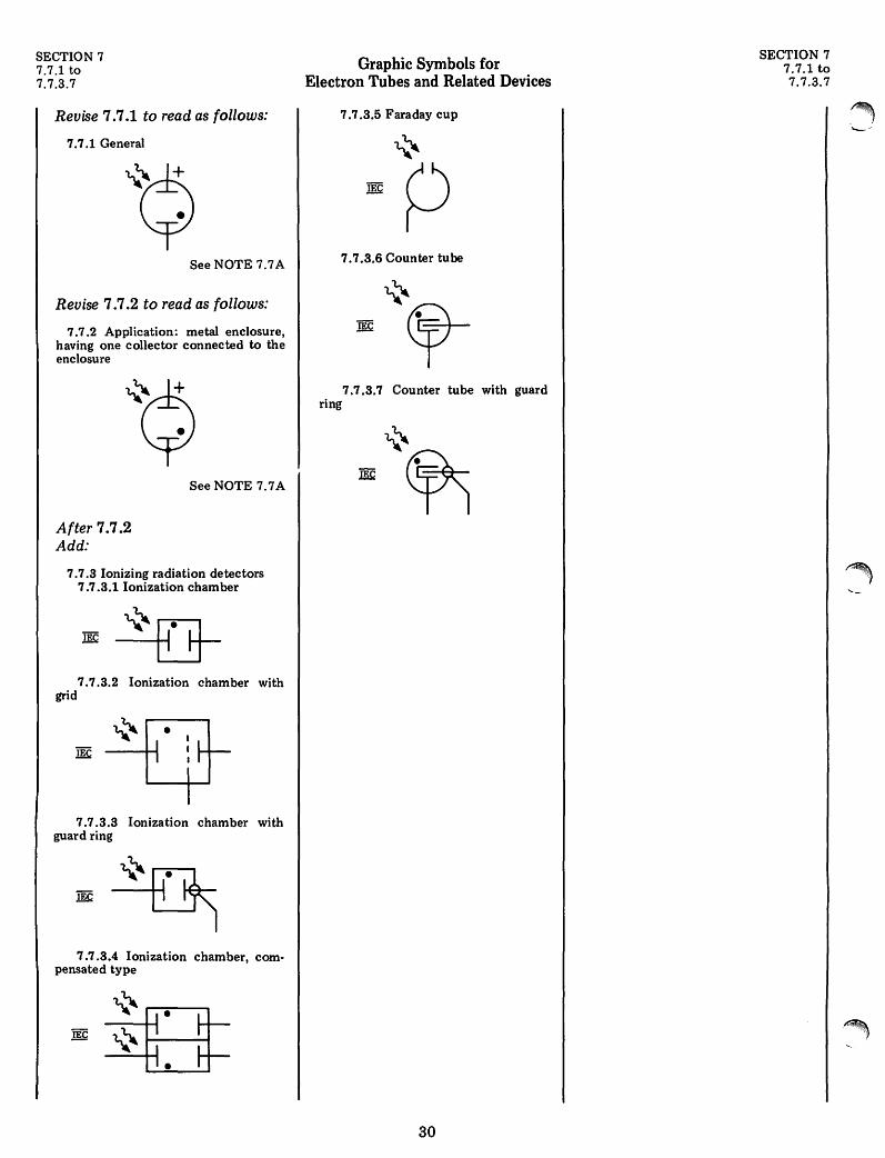
SECTION 7 7.7.1 to 7.7.3.7
Revise 7.7.1 to read as follows:
7.7.1 General
See NOTE 7.7A
Revise 7.7.2 to read as follows:
7.7.2 Application: metal enclosure, having one collector connected to the enclosure
After 7.7.2 Add:
See NOTE 7.7A
7.7.3 Ionizing radiation detectors 7.7.3.1 Ionization chamber
7.7.3.2 Ionization chamber with grid
~.
7.7.3.3 Ionization chamber with guard ring
7.7.3.4 Ionization chamber, compensated type
Graphic Symbols for Electron Tubes and Related Devices
7.7.3.5 Faraday cup
7.7.3.6 Counter tube
7.7.3.7 Counter tube with guard ring
30
SECTION 7 7.7.1 to 7.7.3.7
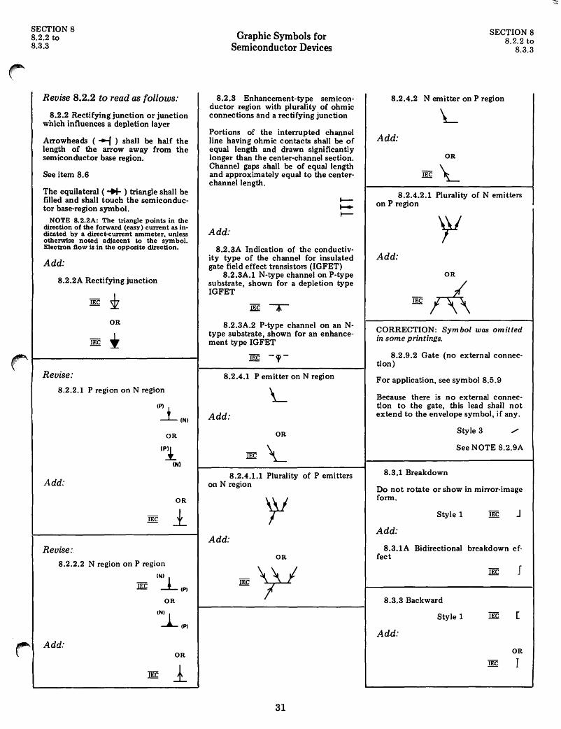
SECTION 8 8.2.2 to 8.3.3
Revise 8.2.2 to read as follows:
8.2.2 Rectifying junction or junction which influences a depletion layer
Arrowheads ( ..., ) shall be half the length of the arrow away from the semiconductor base region.
See item 8.6
The equilateral ( ..... ) triangle shall be filled and shall touch the semiconductor base-region symbol.
NOTE 8.2.2A: The triangle points in the direction of the forward (easy) current as indicated by a ciUect-current ammeter. unless otherwise noted adjacent to the sym bol. Electron flow is in the opposite direction.
Add:
8.2.2A Rectifying junction
OR
Revise:
8.2.2.1 P region on N region
Add:
Revise:
(P)
leN)
OR
(P.l (N)
OR
1
8.2.2.2 N region on P region
Add:
(N) 1 IEC ~(P)
OR
(N) I ~(P)
OR
1
Graphic Symbols for Semiconductor Devices
8.2.3 Enhancement-type semiconductor region with plurality of ohmic connections and a rectifying junction
Portions of the interrupted channel line having ohmic contacts shall be of equal length and drawn significantly longer than the center-channel section. Channel gaps shall be of equal length and approximately equal to the centerchannel length.
Add:
8.2.3A Indication of the conductivity type of the channel for insulated gate field effect transistors (IGFET)
8.2.3A.1 N-type channel on P-type substrate, shown for a depletion type IGFET
8.2.3A.2 P-type channel on an Ntype substrate, shown for an enhancement type IGFET
IEC -,-
8.2.4.1 P emitter on N region
Add:
OR
8.2.4.1.1 Plurality of P emitters on N region
Add:
OR
31
SECTION 8 8.2.2 to
8.3.3
8.2.4.2 N emitter on P region
Add:
OR
8.2.4.2.1 Plurality of N emitters on P region
Add:
OR
CORRECTION: Symbol was omitted in some printings.
8.2.9.2 Gate (no external connection)
For application, see symbol 8.5.9
Because there is no external connection to the gate, this lead shall not extend to the envelope symbol, if any.
Style 3
See NOTE 8.2.9A
8.3.1 Breakdown
Do not rotate or show in mirror-image form.
Style 1 J
Add:
8.3.1A Bidirectional breakdown effect
8.3.3 Backward
Style 1 [
Add:
OR
I
SECI'ION 8 8.3.5 to 8.5.8.3
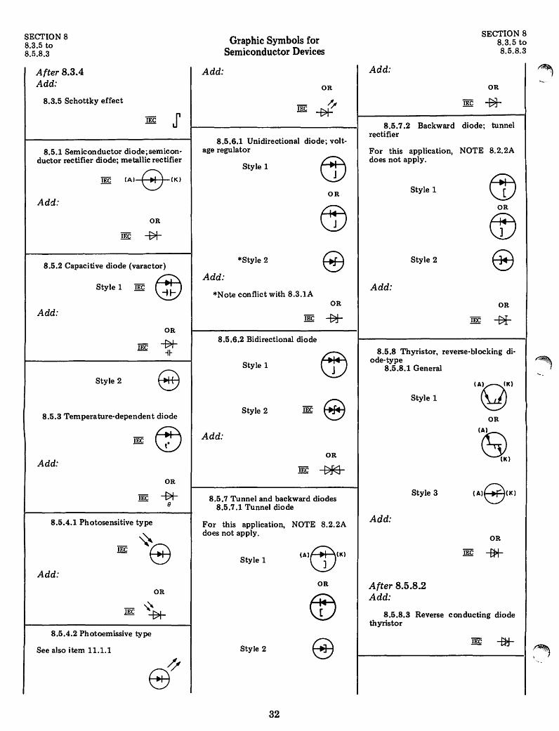
After 8.3.4 Add:
8.3.5 Schottky effect
8.5.1 Semiconductor diode;semicon· ductor rectifier diode; metallic rectifier
lEe (AIB-(KI
Add:
8.5.2 Capacitive diode (varactor)
Style 1 rn; ® Add:
OR
Style 2 8 8.5.3 Temperature·dependent diode
lEe ~ Add:
OR
lEe --t::+-
8.5.4.1 Photosensitive type
Add:
8.5.4.2 Photoemissive type
See also item 11.1.1
8
OR
Graphic Symbols for Semiconductor Devices
Add:
OR
lEe ~ -f7f-
8.5.6.1 Unidirectional diode; volt· age regulator
Style 1 eo OR
eJ *Style 2 8
Add:
*Note conflict with 8.3.1A OR
lEe ~
8.5.6.2 Bidirectional diode
Style 1 (f)
Style 2 lEe (3 Add:
OR
IEC ~
8.5.7 Tunnel and backward diodes 8.5.7.1 Tunnel diode
For this application, NOTE 8.2.2A does not apply.
Style 1 ,A'ffi,K' OR
® Style 2 8
32
SECTION 8 8.3.5 to 8.5.8.3
Add: ~ OR
lEe ~
8.5.7.2 Backward diode; tunnel rectifier
For this application, NOTE 8.2.2A does not apply.
Style 1 eo OR
eo Style 2 e
Add:
OR
lEe -B*-
8.5.8 Thyristor, reverse-blocking di· ode·type ~ 8.5.8.1 General
Style 1 IAg/ OR
I~ (K)
Style 3 (A)8(K)
Add:
OR
lEe -a+
After 8.5.8.2 Add:
8.5.8.3 Reverse conducting diode thyristor
~ --EM-.~ \
SECTION 8 8.5.9 to 8.S.l0.IA
8.5.9 Thyristor, bidirectional diode type; bi·switch
See also symbol 8.6.15
Add:
OR
Add:
8:5.11 Current regulator
* (A) -~"~1f.-- (K)
*Note conflict with 8.3.3
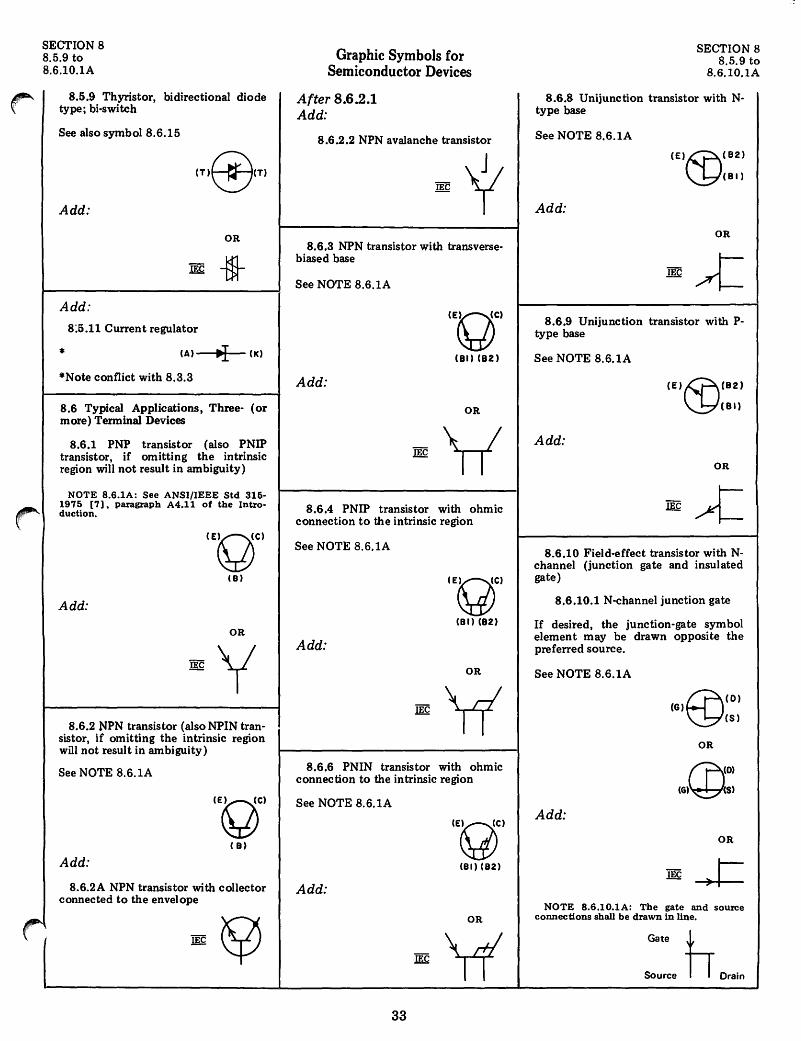
8.6 Typical Applications, Three· (or more) Terminal Devices
8.6.1 PNP transistor (also PNIP transistor, if omitting the intrinsic region will not result in ambiguity)
NOTE 8.6.IA: See ANSI/IEEE Std 315· 1975 (7). paragraph A4.11 of the Intro· duction.
Add:
OR
8.6.2 NPN transistor (also NPIN tran· sistor, if omitting the intrinsic region will not result in ambiguity)
See NOTE 8.6.lA
Add:
8.6.2A NPN transistor with collector connected to the envelope
Graphic Symbols for Semiconductor Devices
After 8.6.2.1 Add:
8.6.2.2 NPN avalanche transistor
8.6.3 NPN transistor with transverse· biased base
See NOTE 8.S.lA
(E'Q/ (BI) (B2)
Add:
OR
8.6.4 PNIP transistor with ohmic connection to the intrinsic region
See NOTE 8.S.IA
(E~Jr (81) (B2)
Add:
OR
8.6.6 PNIN transistor with ohmic connection to the intrinsic region
See NOTE 8. S.lA
(E~C'
(81) (B2)
Add:
OR
33
SECTION 8 8.5.9 to
8.S.l0.lA
8.6.8 Unijunction transistor with N· type base
See NOTE 8.S.lA
Add:
(E't<:P\(B2)
W(BI)
OR
8.6.9 Unijunction transistor with p. type base
See NOTE 8.6.lA
Add:
(E)~(B2)
\.J:;,I ( B I )
OR
8.6.10 Field~ffect transistor with N· channel (junction gate and insulated gate)
8.6.10.1 N·channel junction gate
If desired, the junction·gate symbol element may be drawn opposite the preferred source.
See NOTE 8.6.lA
Add:
@(o) (6)
(S)
OR
f?\(0)
(6),&\S)
OR
NOTE 8.6.10.1A: The gate and source connections shall be drawn in line.
Gate L Source n Drain
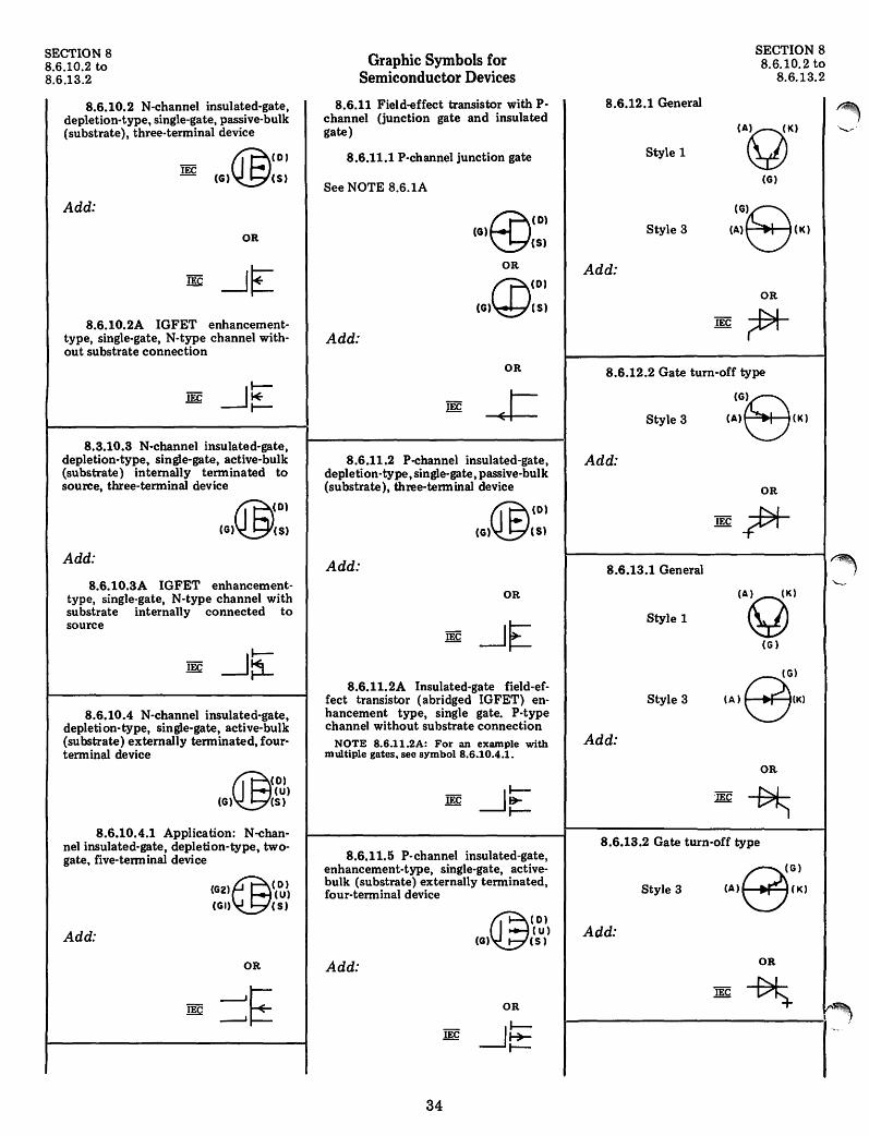
SECTION 8 8.6.10.2 to 8.6.13.2
8.6.10.2 N-channel insulated-gate, depletion-type, single-gate, passive-bulk (substrate), three-terminal device
lEe @IDI
(G) (S)
Add:
OR
lEe ~~ 8.6.10.2A IGFET enhancement-
type, single-gate, N-type channel with-out substrate connection
lEe ~~ 8.3.10.3 N-channel insulated-gate,
depletion-type, single-gate, active-bulk (substrate ) internally terminated to source, three-terminal device
@IDI (G) (S)
Add:
8.6.10.3A IGFET enhancement-type, single-gate, N-type channel with substrate internally connected to source
lEe ~$= 8.6.10.4 N-channel insulated-gate,
depletion-type, single-gate, active-bulk (substrate) externally terminated, four-terminal device
@ID) (U)
(G) (S)
8.6.10.4.1 Application: N-chan-nel insulated-gate, depletion-type, two-gate, five-terminal device
IG21~IDI (U) (GI) (S)
Add:
OR
lEe ~~
Graphic Symbols for Semiconductor Devices
8.6.11 Field-effect transistor with P-channel (junction gate and insulated gate)
8.6.11.1 P-channel junction gate
See NOTE 8.6.1A
EQIDI (6) (S)
OR
Q)IDI (G) (S)
Add:
OR
lEe --J= 8.6.11.2 P-channel insulated-gate,
depletion-type, single-gate, passive-bulk (substrate), three-terminal device
@IDI (G) (5)
Add:
OR
lEe ~~ 8.6.11.2A Insulated-gate field-ef-
feet transistor (abridged IGFET) en-hancement type, single gate. P-type channel without substrate connection
NOTE 8.6.11.2A: For an example with multiple gates, see symbol 8.6.10.4.1.
lEe ~~
8.6.11.5 P-channel insulated-gate, enhancement-type, single-gate, active-bulk (substrate) externally terminated, four-terminal device
@IDI (u)
(G) (S)
Add:
OR
lEe ~~ t--
34
8.6.12.1 General
Style 1
Style 3
Add:
SECTION 8 8.6.10.2 to
8.6.13.2
IAlr;;)/ (G)
'G8 (A) (K)
OR
lEe ~ 8.6.12.2 Gate tum-off type
Style 3 'G8 (A) (K)
Add:
OR
lEe ~ 8.6.13.1 General
Style 1 IA~)
(G)
(G)
IAlel.) Style 3
Add:
OR
m ~ 8.6.13.2 Gate turn-off type
Style 3 eGI (A) (K)
Add:
OR
lEe ~
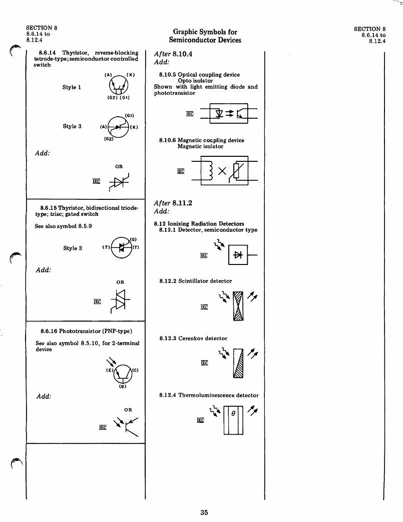
SECTION 8 8.6.14 to 8.12.4
8.6.14 Thyristor, reverse-blocking tetrode-type; sem iconductor con trolled switch
Style 1
Style 3
Add:
OR
8.6.15 Thyristor, bidirectional triodetype; triac; gated switch
See also symboIS.5.9
Style 3 ~G)
(T)~(T)
Add:
OR
8.6.16 Phototransistor (PNP-type)
See also symbol S.5.10, for 2-terminal device
Add:
OR
Graphic Symbols for Semiconductor Devices
After 8.10.4 Add:
8.10.5 Optical coupling device Opto isolator
Shown with light emitting diode and photo transistor
8.10.6 Magnetic coupling device Magnetic isolator
After 8.11.2 Add:
8.12 Ionizing Radiation Detectors 8.12.1 Detector, semiconductor type
8.12.2 Scintillator detector
8.12.3 Cerenkov detector
8.12.4 Thermoluminescence detector
35
SECTION 8 8.6.14 to
8.12.4
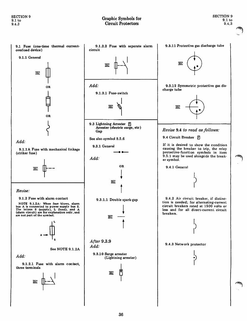
SECTION 9 9.1 to 9.4.3
9.1 Fuse (one-time thermal currentoverload device)
9.1.1 General
OR
OR
Add:
9.1.1A Fuse with mechanical linkage (striker fuse)
Revise:
9.1.2 Fuse with alarm contact NOTE 9.1.2A: When fuse blows, alarm
bus A is connected to power supply bus S. The letters S (supply), L (load), and A (alann circuit) are for explanation only, and are not part of the sym boI.
See NOTE 9.1.2A
Add:
9.1.2.1 Fuse with alarm contact, three term inals
Graphic Symbols for Circuit Protectors
9.1.2.2 Fuse with separate alarm circuit
Add:
9.1.3.1 Fuse-switch
9.3 Ligh tning Arrester El Arrester (electric surge, etc) Gap
See also symbol 8.5.6
9.3.1 General
Add:
OR
9.3.1.1 Double spark-gap
lEe
After 9.3.9 Add:
! f
9.3.10 Surge arrester (Lightning arrester)
36
SECTION 9 9.1 to 9.4.3
9.3.11 Protective gas discharge tube
9.3.12 Symmetric protective gas discharge tube
Revise 9.4 to read as follows:
9.4 Circuit Breaker EJ
If it is desired to show the condition causing the breaker to trip, the relay protective-function symbols in item 9.5.1 may be used alongside the breaker symbol.
9.4.1 General
9.4.2 Air circuit breaker, if distinction is needed; for alternating-current circuit breakers rated at 1500 volts or less and for all direct-current circuit breakers.
9.4.3 Network protector
~ ••• . ~ .. \J
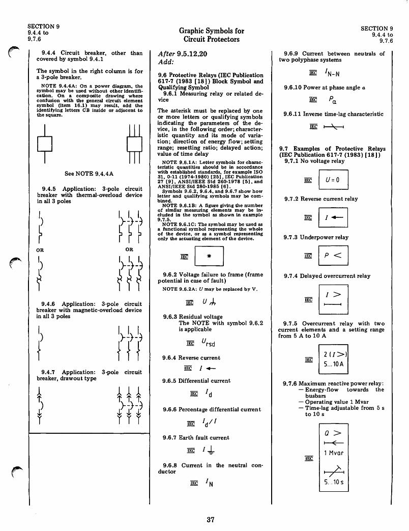
(".
SECTION 9 9.4.4 to 9.7.6
9.4.4 Circuit breaker, other than covered by symbol 9.4.1
The symbol in the right column is for a 3-pole breaker.
NOTE 9.4.4A: On a power diagram, the symbol may be used without other identification. On a composite drawing where confusion with the general circuit element symbol (item IS.1) may result, add the identifying letters CB inside or adjacent to the square.
See NOTE 9.4.4A
9.4.5 Application: 3-pole circuit breaker with thermal-overload device in all 3 poles
')
~ 1)-!)_11
~ ~ ~ OR OR
I)
f 1)-~)_11
f f f 9.4.6 Application: 3-pole circuit
breaker with magnetic-overload device in all 3 poles
9.4.7 Application: 3-pole circuit breaker, drawout type
Graphic Symbols for Circuit Protectors
After 9.5.12.20 Add:
9.6 Protective Relays (IEC Publication 617-7 (1983 [18]) Block Symbol and Qualifying Symbol
9.6.1 Measuring relay or related device
The asterisk must be replaced by one or more letters or qualifying symbols indicating the parameters of the device, in the following order; characteristic quantity and its mode of variation; direction of energy flow; setting range; resetting ratio; delayed action; value of time delay
NOTE 9.S.1A: Letter symbols for characteristic quantities should be in accordance with established standards, for example ISO 31, 0-11 (1974-1980) [25] • IEC Publication 27 [9], ANSIIIEEE Std 2S0-1978 [5], and ANSI{IEEE Std 280-1985 [S] .
Symbols 9.S.2, 9.S.4, and 9.S.7 show how letter and qualifying symbols may be combined.
NOTE 9.S.1B: A figure giving the number of similar measuring elements may be included in the symbol as shown in example 9.7.5.
NOTE 9.S.1C: The symbol may be used as a functional symbol representing the whole of the device, or as a symbol representing only the actuating element of the device.
9.6.2 Voltage failure to frame (frame potential in case of fault)
NOTE 9.S.2A: U may be replaced by V.
9.6.3 Residual voltage The NOTE with symbol 9.6.2 is applicable
lEe Ursd
9.6.4 Reverse current
~ 1.-
9.6.5 Differential current
9.6.6 Percentage differential current
9.6.7 Earth fault current
lEe 1 ~
9.6.8 Current in the neutral conductor
37
SECTION 9 9.4.4 to
9.7.6
9.6.9 Current between neutrals of two polyphase systems
lEe IN- N
9.6.10 Power at phase angle a
~ Pu
9.6.11 Inverse time-lag characteristic
9.7 Examples of Protective Relays (IEC Publication 617-7 (1983) [18])
9.7.1 No voltage relay
9.7.2 Reverse current relay
9.7.3 U nderpower relay
9.7.4 Delayed overcurrent relay
-8> lEe - t------4
9.7.5 Overcurrent relay with two current elemen ts and a setting range from 5 A to lOA
2 (I»
5 ... 10A
9.7.6 Maximum reactive power relay: - Energy-flow towards the
busbars - Operating value 1 Mvar - Time-lag adjustable from 5 s
to 10 s
a> ~
1 Mvar IEC
+ 5 ... 10 s
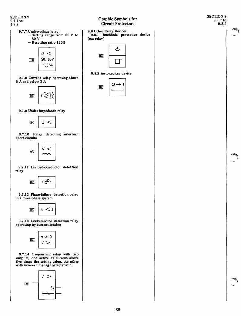
SECTION 9 9.7.7 to 9.S.2
9.7.7 Undervoltage relay: - Setting range from 50 V to
SOV - Resetting ratio 130%
u< IEC SO ... 80V
130 0/0
9.7.8 Current relay operating above 5 A and below 3 A
-II>SAI .If&. < 3A
9.7.9 Under-impedance relay
9.7.10 Relay detecting interturn short-circuits
9.7.11 Divided-conductor detection relay
9.7.12 Phase-failure detection relay in a three-phase system
lEe B 9.7.13 Locked-rotor detection relay
operating by current sensing
_§~O IEC - I>
9.7.14 Overcurrent relay with two outputs, one active at current above five times the setting value, the other with inverse time-lag characteristic
I>
Graphic Symbols for Circuit Protectors
9.8 Other Relay Devices 9.8.1 Buchholz protective device
(gas relay)
9.8.2 Auto-reclose device
38
SECTION 9 9.7.7 to
9.8.2
~.". 0'.)
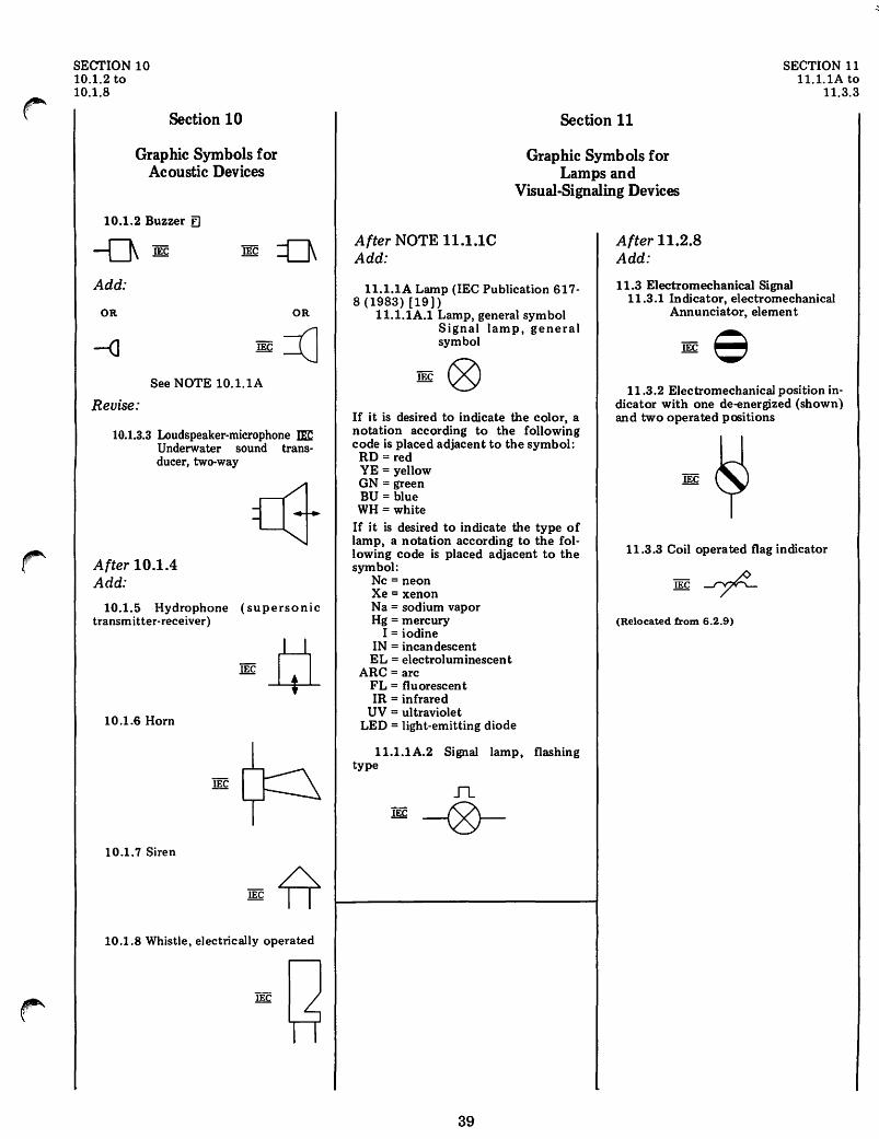
SECTION 10 10.1.2 to 10.1.8
Section 10
Graphic Symbols for Acoustic Devices
10.1.2 Buzzer [)
-0 lEe
Add:
OR
-(]
See NOTE 10.1.lA
Revise:
OR
10.1.3.3 Loudspeaker-microphone IE Underwater sound transducer, two-way
After 10.1.4 Add:
10.1.5 Hydrophone (supersonic transmitter-receiver)
10.1.6 Horn
10.1.7 Siren
10.1.8 Whistle, electrically operated
SECTION 11 11.1.lA to
11.3.3
Section 11
Graphic Symbols for Lamps and
Visual-Signaling Devices
After NOTE l1.l.1e Add:
11.1.1A Lamp (IEC Publication 617-8 (1983) [19])
11.1.1A.1 Lamp, general symbol Signal lamp, general symbol
If it is desired to indicate the color, a notation according to the following code is placed adjacent to the symbol:
RD:;;: red YE:;;: yellow GN::: green BU:;;: blue WH::: white
If it is desired to indicate the type of lamp, a notation according to the following code is placed adjacent to the symbol:
Nc:;;: neon Xe:;;: xenon Na = sodium vapor Hg = mercury
I = iodine IN = incandescent EL = electroluminescent
ARC = arc FL = fluorescent IR = infrared
UV ::: ultraviolet LED = light-emitting diode
11.1.1A.2 Signal lamp, flashing type
39
After 11.2.8 Add:
11.3 Electromechanical Signal 11.3.1 Indicator, electromechanical
Annunciator, element
11.3.2 Electromechanical position indicator with one de-energized (shown) and two operated positions
11.3.3 Coil operated flag indicator
(Relocated from 6.2.9)
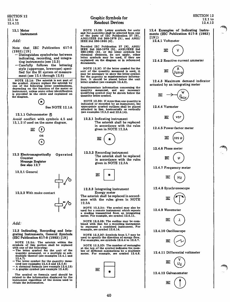
SECTION 12 12.1 to 12.4.12
12.1 Meter Instrument
Add:
Note that IEC Publication 617-8 (1983) [19]
- Distinguishes symbol wise between indicating, recording, and integrating instruments (see 12.3)
- Carefully follows the lettering style (uppercase, lowercase) specified for the SI system of measurement (see 12.4 through 12.6)
NOTE 12.1A: The asterisk is not part of the symbol. Always replace the asterisk by one of the following letter combinations, depending on the function of the meter or instrument, unless some other identification is provided in the circle and explained on the diagram. o
See NOTE 12.1A
12.1.1 Galvanometer f1 Avoid conflict with symbols 4.5 and 13.1.2 if used on the same diagram.
IEC CD OR
12.2 Electromagnetically Operated Counter Message Register See also 12.7
12.2.1 General
12.2.2 With make contact
Add:
12.3 Indicating, Recording and Integrating Instruments, General Symbols (IEC Publication 617-8 (1983) [19]
NOTE 12.3A: The asterisk within the symbols of this section shall be replaced with one of the following: - The letter symbol for the unit of the
quantity measured, or a multiple or submultiple thereof (see examples 12.4.1 and 12.4.7)
- The letter symbol for the quantity measured (see examples 12.4.5 and 12.4.6)
- A chemical formula (see example 12.4.13) - A graphic symbol (see example 12.4.8)
The symbol or formula used should be related to the information displayed by the instrument regardless of the means used to obtain the information.
Graphic Symbols for Readout Devices
NOTE 12.3B: Letter symbols for units and for quantities shall be selected from one of the parts of IEC Publication 27 [9], ANSI/IEEE Std 260-1978 [5], and ANSI/ IEEE Std 280-1986 [6] •
Provided IEC Publication 27 [9], ANSI/ IEEE Std 260-1978 [5], ANSI/IEEE Std 280-1986 [6], or the letter symbols for chemical elements, do not apply, other letter symbols may be used, if they are explained on the diagram or in referenced documents.
NOTE 12.3C: If the letter symbol for the unit of the quantity measured is used, it may be necessary to show the letter symbol for the quantity as supplementary information. It should be placed below the unit letter symbol (see example 12.4.2).
Supplementary information concerning the quantity measured, and any necessary qualifying symbol may be shown below the quantity letter symbol.
NOTE 12.30: If more than one quantity is indicated or recorded by an instrument, the appropriate symbol outlines shall be placed attached in line, horizontally or vertically (see examples 12.5.2 and 12.6.14).
12.3.1 Indicating instrument The asterisk shall be replaced in accordance with the rules given in NOTE 12.3A
12.3.2 Recording instrument The asterisk shall be replaced in accordance with the rules given in NOTE 12.3A
12.3.3 Integrating instrument Energy meter
The asterisk shall be replaced in accordance with the rules given in NOTE 12.3A
NOTE 12.3.3A: The symbol may also be used for a remote instrument which repeats a reading transmitted from an integrating meter. For example, see symbol 12.6.11.
NOTE 12.3.3B: The outline may be combined with that for a recording instrument to represent a combined instrument. For example, see symbol 12.6.14.
NOTE 12.3.3C: Symbols from 1.7 may be used to specify the direction of energy flow. For examples, see symbols 12.6.4 to 12.6.7.
NOTE 12.3.30: The number of rectangles at the top of the symbol indicates the number of different summations by a multirate meter. For example, see symbol 12.4.8.
40
SECTION 12 12.1 to 12.4.12
12.4 Examples of Indicating Instruments (lEC Publication 617-8 (1983) [19] )
12.4.1 Voltmeter
12.4.2 Reactive current ammeter
IEC a\ ~
12.4.3 Maximum demand indicator actuated by an integrating meter
IEC~ '~
12.4.4 Varmeter
meG 12.4.5 Power-factor meter
lEe 8 12.4.6 Phase meter
12.4.7 Frequency meter
lEe G) 12.4.8 Synchronoscope
12.4.9 Wavemeter
12.4.10 Oscilloscope
12.4.11 Differential voltmeter
lEe G) 12.4.12 Galvanometer
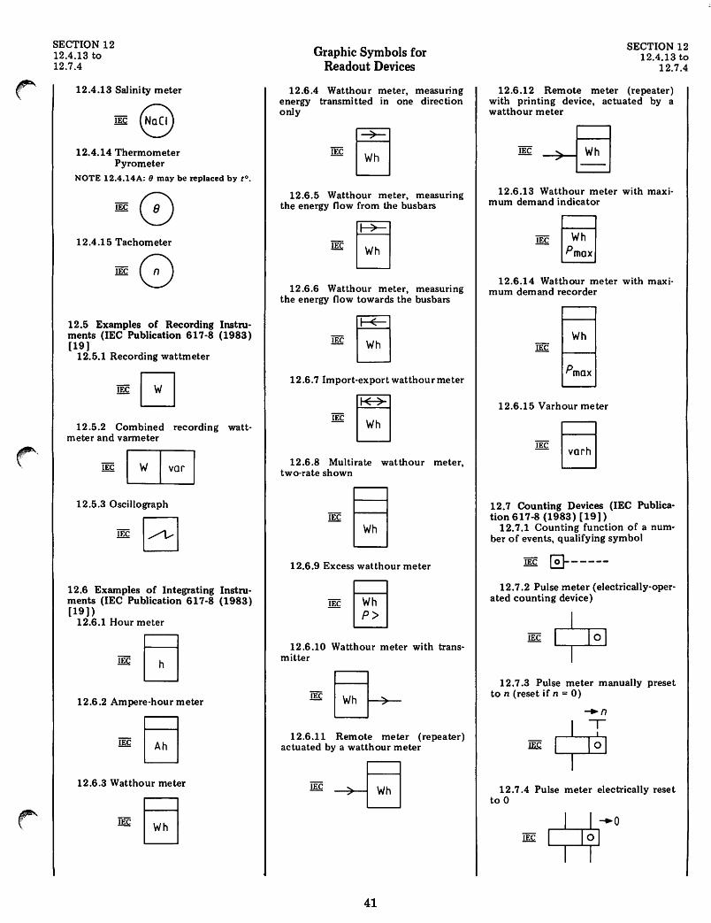
SECTION 12 12.4.13 to 12.7.4
12.4.13 Salinity meter
~8 12.4.14 Thermometer
Pyrometer NOTE 12.4.14A: (J may be replaced by to.
12.4.15 Tachometer
12.5 Examples of Recording Instruments (lEe Publication 617-8 (1983) [19 ]
12.5.1 Recording wattmeter
12.5.2 Combined recording watt· meter and vanneter
IECB 12.5.3 Oscillograph
12.6 Examples of Integrating Instruments (lEe Publication 617-8 (1983) [19])
12.6.1 Hour meter
12.6.2 Ampere-hour meter
12.6.3 Watthour meter
Graphic Symbols for Readout Devices
12.6.4 Watthour meter, measuring energy transmitted in one direction only
12.6.5 Watthour meter, measuring the energy flow from the bus bars
12.6.6 Watthour meter, measuring the energy flow towards the bus bars
12.6.7 Import-export waUhour meter
12.6.8 Multirate watthour meter, two-rate shown
12.6.9 Excess watthour meter
lEe ~ ~
12.6.10 Watthour meter with transmitter
12.6.11 Remote meter (repeater) actuated by a watthour meter
41
SECTION 12 12.4.13 to
12.7.4
12.6.12 Remote meter (repeater) with printing device, actuated by a watthour meter
12.6.13 Watthour meter with maxi· mum demand indicator
IEC ~ ~
12.6.14 Wat.thour meter with maximum demand recorder
Wh
Pmax
12.6.15 Varhour meter
lEe R ~
12.7 Counting Devices (lEe Publication 617-8 (1983) [19])
12.7.1 Counting function of a number of events, qualifying symbol
lEe 0------12.7.2 Pulse meter (electrically-oper
ated counting device)
12.7.3 Pulse meter manually preset to n (reset if n :;: 0)
12.7.4 Pulse meter electrically reset to 0
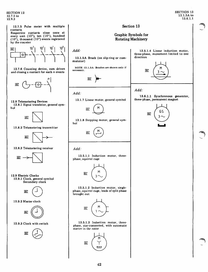
SECTION 12 12.7.5 to 12.9.3
12.7.5 Pulse meter with multiple contacts Respective contacts close once at every unit (10 0
), ten (10 1), hundred
(102), thousand (10 3) events registered
by the counter
12.7.6 Counting device, cam driven and closing a contact for each n events
12.8 Telemetering Devices 12.8.1 Signal translator, general sym
bol
12.8.2 Telemetering transmitter
12.8.3 Telemetering receiver
12.9 Electric Clocks 12.9.1 Clock, general symbol
Secondary clock
12.9.2 Master clock
12.9.3 Clock with switch
SECTION 13 13.1.5A to
13.6.1.1
Section 13
Graphic Symbols for Rotating Machinery
Add:
13.1.5A Brush (on slip-ring or commutator)
NOTE 13.1.5A: Brushes are shown only if necessary.
Add:
13.1.7 Linear motor, general symbol
13.1.8 Stepping motor, general sym· bol
Add:
13.5.1.1 Induction motor, three· phase, squirrel cage
13.5.1.2 Induction motor, single· phase, squirrel cage, leads of split phase brought out
13.5.1.3 Induction motor, threephase, star·connected, with automatic starter in the rotor
42
13.5.1.4 Linear induction motor, three-phase, movement limited to one direction
Add:
13.6.1.1 Synchronous generator, three-phase, permanent magnet
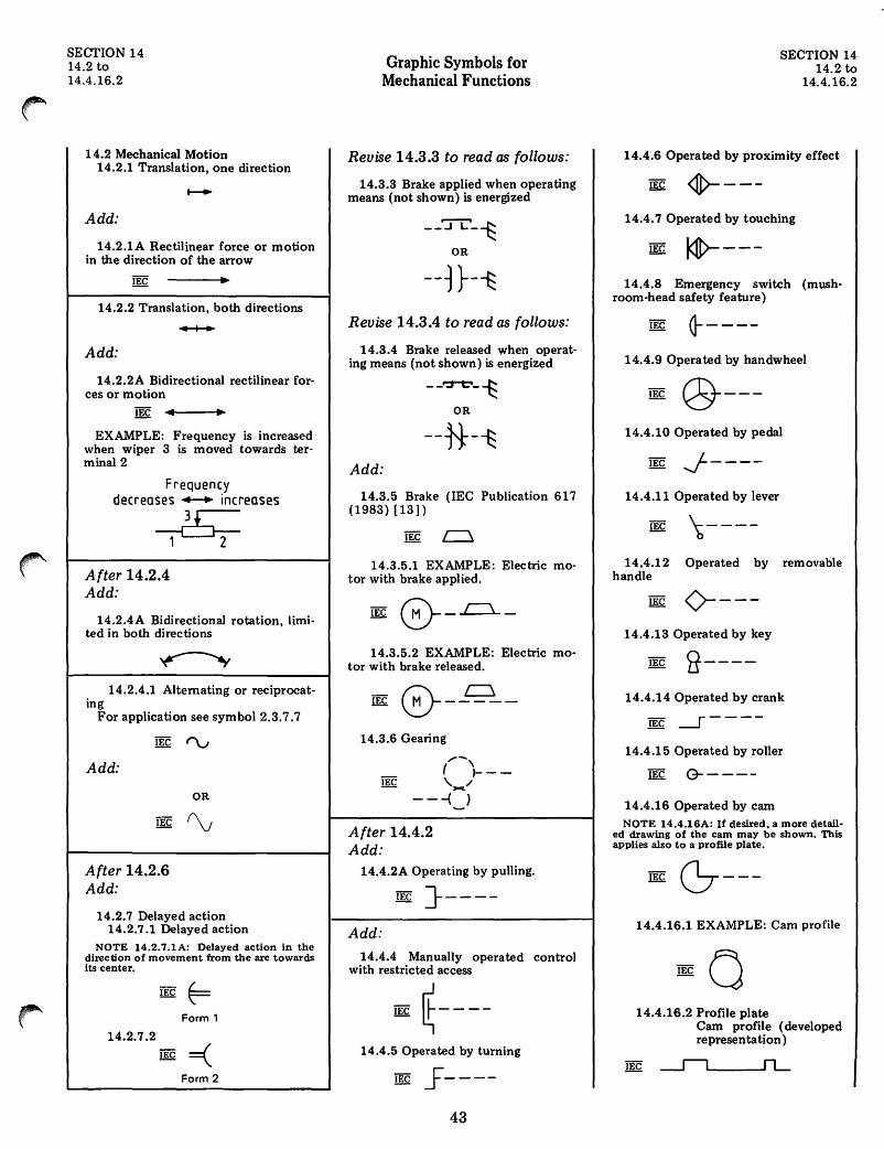
SECTION 14 14.2 to 14.4.16.2
14.2 Mechanical Motion 14.2.1 Translation, one direction
Add:
14.2.1A Rectilinear force or motion in the direction of the arrow
14.2.2 Translation, both directions
~
Add:
14.2.2A Bidirectional rectilinear forces or motion
IEC It ..
EXAMPLE: Frequency is increased when wiper 3 is moved towards terminal2
Frequency decreases ..-. increases
~ After 14.2.4 Add:
14.2.4A Bidirectional rotation, limited in both directions
14.2.4.1 Alternating or reciprocating
For application see symbol 2.3.7.7
IEC rv Add:
OR
After 14.2.6 Add:
14.2.7 Delayed action 14.2.7.1 Delayed action
NOTE 14.2.7.1A: Delayed action in the direction of movement from the arc towards its center.
14.2.7.2
IEC €= Form 1
IEC ==( Form 2
Graphic Symbols for Mechanical Functions
Revise 14.3.3 to read as follows:
14.3.3 Brake applied when operating means (not shown) is energized
__ .J L_~
OR
--1 }-~ Revise 14.3.4 to read as follows:
14.3.4 Brake released when operating means (not shown) is energized
__ 'Tt"_~
OR
--t}-~ Add:
14.3.5 Brake (IEC Publication 617 (1983) [13])
14.3.5.1 EXAMPLE: Electric motor with brake applied.
IEC 0--~-
14.3.5.2 EXAMPLE: Electric motor with brake released.
- r::L ~ IEC ~-----
14.3.6 Gearing
( .... -'r---'-./
---{-)
After 14.4.2 Add:
14.4.2A Operating by pulling.
IEC }----
Add:
14.4.4 Manually operated control with restricted access
lEe ~----14.4.5 Operated by turning
IEC 5----43
SECTION 14 14.2 to
14.4.16.2
14.4.6 Operated by proximity effect
IEC ~---
14.4.7 Operated by touching
IEC I<lJr - - -14.4.8 Emergency switch (mush
room-head safety feature)
(}-----14.4.9 Operated by handwheel
IEC @----14.4.10 Operated by pedal
IEC J----14.4.11 Operated by lever
IEC \----
14.4.12 Operated by removable handle
IEC 0----14.4.13 Operated by key
IEC 9-----14.4.14 Operated by crank
IEC ---I - ---
14.4.15 Operated by roller
IEC G-----
14.4.16 Operated by cam NOTE 14.4.1SA: If desired, a more detail
ed drawing of the cam may be shown. This applies also to a profile plate.
IEC ~---
14.4.16.1 EXAMPLE: Cam profile
14.4.16.2 Profile plate Cam profile (developed representation)
IEC~
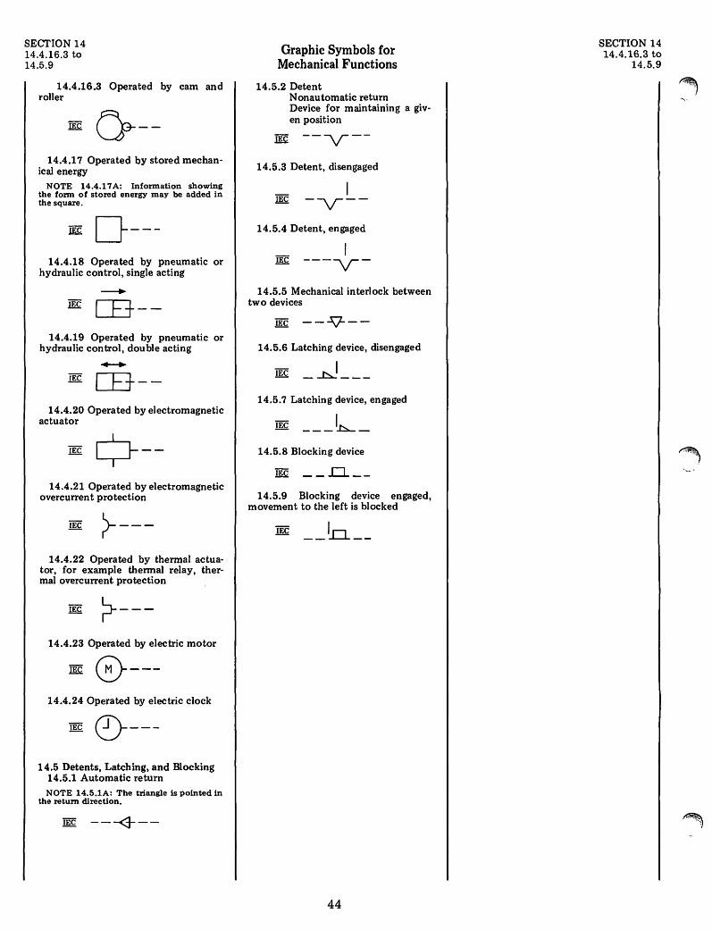
SECI'ION 14 14.4.16.3 to 14.5.9
14.4.16.3 Operated by cam and roller
IEC 0---14.4.17 Operated by stored mechan
ical energy NOTE 14.4.17 A: Information showing
the form of stored energy may be added in the square.
~ 0---14.4.18 Operated by pneumatic or
hydraulic control, single acting
[8--14.4.19 Operated by pneumatic or
hydraulic control, double acting
.....-.. lEe [8--
14.4.20 Operated by electromagnetic actuator
IEC Q---14.4.21 Operated by electromagnetic
overcurrent protection
>----14.4.22 Operated by thermal actua
tor, for example thermal relay, thermal overcurrent protection
lEe ?----14.4.23 Operated by electric motor
lEe 0---14.4.24 Operated by electric clock
lEe ~---
14.5 Detents, Latching, and Blocking 14.5.1 Automatic return NOTE 14.5.1A: The triangle is pointed in
the return direction.
IEC ---<9---
Graphic Symbols for Mechanical Functions
14.5.2 Detent Nonautomatic return Device for maintaining a given position
lEe ---y---
14.5.3 Detent, disengaged
I -y---
14.5.4 Detent, engaged
I ----y-
14.5.5 Mechanical interlock between two devices
IEC - - s::}- - -
14.5.6 Latching device, disengaged
I -~---
14.5.7 Latching device, engaged
I ---~-
14.5.8 Blocking device
lEe __ ..D.. __
14.5.9 Blocking device engaged, movement to the left is blocked
lEe __ ~ __
44
SECTION 14 14.4.16.3 to
14.5.9
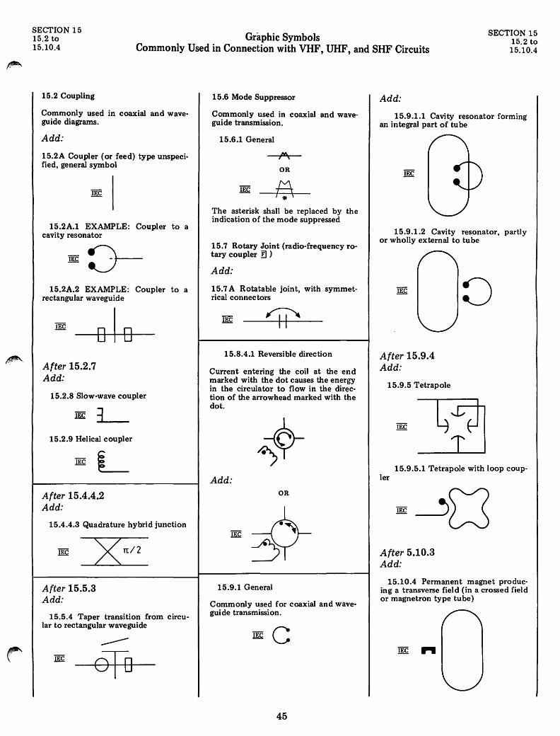
" ..
Graphic Symbols SECTION 15 15.2 to 15.10.4 Commonly Used in Connection with VHF, UHF, and SHF Circuits
SECTION 15 15.2 to 15.1004
15.2 Coupling
Commonly used in coaxial and waveguide diagrams.
Add:
15.2A Coupler (or feed) type unspecified, general symbol
15.2A.1 EXAMPLE: Coupler to a cavity resonator
15.2A.2 EXAMPLE: Coupler to a rectangular waveguide
After 15.2.7 Add:
010
15.2.8 Slow-wave coupler
lEe _3~ __ 15.2.9 Helical coupler
IEC L After 15.4.4.2 Add:
15.4.4.3 Quadrature hybrid junction
IEC >< !t/2
After 15.5.3 Add:
15.5.4 Taper transition from circular to rectangUlar waveguide
15.6 Mode Suppressor
Commonly used in coaxial and waveguide transmission.
15.6.1 General
I -.
\
OR
lEe {-f\ The asterisk shall be replaced by the indication of the mode suppressed
15.7 Rotary Joint (radio-frequency rotary coupler fI )
Add:
15.7 A Rotatable joint, with symmetrical connectors
15.8.4.1 Reversible direction
Current entering the coil at the end marked with the dot causes the energy in the circulator to flow in the direction of the arrowhead marked with the dot.
Add: OR
15.9.1 General
Commonly used for coaxial and waveguide transmission.
~C
45
Add:
15.9.1.1 Cavity resonator forming an integral part of tube
lEe
15.9.1.2 Cavity resonator, partly or wholly external to tube
After 15.9.4 Add:
15.9.5 Tetrapole
15.9.5.1 Tetrapole with loop coup-ler
After 5.10.3 Add:
15.10.4 Permanent magnet producing a transverse field (in a crossed field or magnetron type tube)
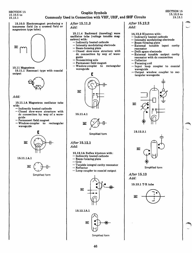
SECTION 15 Graphic Symbols ~t~~:~ to Commonly Used in Connection with VHF, UHF, and SHF Circuits
SECTION 15 15.10.5 to
15.13.1
15.10.5 Electromagnet producing a After 15.11.3 After 15.12.2 transverse field (in a crossed field or Add: Add: magnetron type tube)
n 15.11 Magnetron
15.11.1 Resonant type with coaxial output
Add:
15.11.1A Magnetron oscillator tube with:
- Indirectly heated cathode - Closed slow-wave structure with
dc connection by way of a waveguide
- Permanent field magnet - Window-coupler to rectangular
waveguide
15.11.1A.1
Simplified form
15.11.4 Backward (traveling) wave oscillator tube (voltage tunable magnetron) with:
- Indirectly heated cathode - Intensity modulating electrode - Beam-forming plate - Closed slow-wave structure with
dc connection by way of waveguide
- Nonemitting sole - Permanent field magnet - Window-coupler to rectangular
waveguide
15.11.4.1
~c 0--e-u Simplified form
After 15.12.1 Add:
15.12.1A Reflex klystron with: - Indirectly heated cathode - Beam-forming plate -Grid - Tunable integral cavity resonator - Reflector - Loop coupler to coaxial output
15.12.1A.1
Simplified form
46
15.12.3 Klystron with: - Indirectly heated cathode - Intensity modulating electrode - Beam-forming plate - External tunable input cavity
resonator - Drift space electrode - External tunable output cavity
resonator with dc connection - Collector - Focusing coil - Input loop coupler to coaxial
waveguide - Output window coupler to rec
tangular waveguide
15.12.3.1
Simplified form
After 15.13 Add:
15.13.1 T-R tube
~". IEC~
----
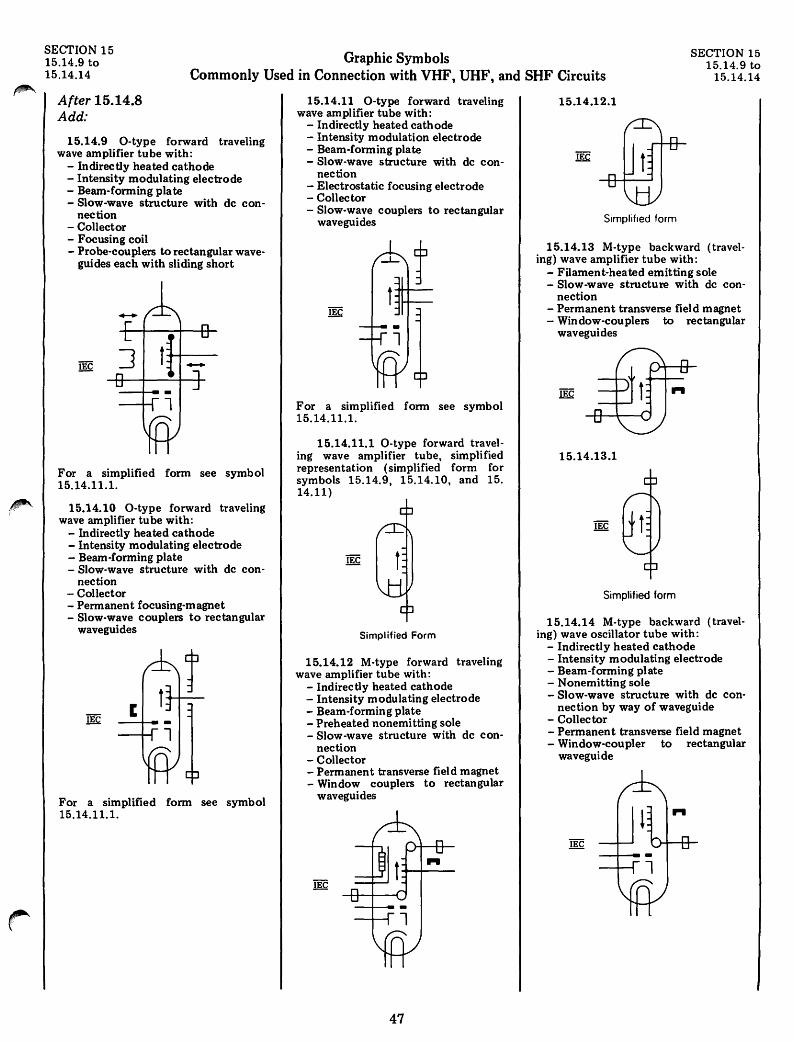
Graphic Symbols SECTION 15 15.14.9 to 15.14.14 Commonly Used in Connection with VHF, UHF, and SHF Circuits
SECTION 15 15.14.9 to
15.14.14
After 15.14.8 Add:
15.14.9 O-type forward traveling wave amplifier tube with:
- Indirectly heated cathode - Intensity modulating electrode - Beam-forming plate - Slow-wave structure with dc con-
nection - Collector - Focusing coil - Probe-couplers to rectangular wave-
guides each with sliding short
For a simplified form see symbol 15.14.11.1.
15.14.10 O-type forward traveling wave amplifier tube with:
- Indirectly heated cathode - Intensity modulating electrode - Beam-forming plate - Slow-wave structure with dc con-
nection - Collector - Permanent focusing-magnet - Slow-wave couplers to rectangular
waveguides
For a simplified form see symbol 15.14.11.1.
15.14.11 O-type forward traveling wave amplifier tube with:
- Indirectly heated cathode - Intensity modulation electrode - Beam-forming plate - Slow-wave structure with dc con-
nection - Electrostatic focusing electrode - Collector - Slow-wave couplers to rectangular
waveguides
For a simplified form see symbol 15.14.11.1.
15.14.11.1 O-type forward traveling wave amplifier tube, simplified representation (simplified form for symbols 15.14.9, 15.14.10, and 15. 14.11)
Simplified Form
15.14.12 M-type forward traveling wave amplifier tube with:
- Indirectly heated cathode - Intensity modulating electrode - Beam-forming plate - Preheated nonemitting sole - Slow-wave structure with dc con-
nection - Collector - Permanent transverse field magnet - Window couplers to rectangular
waveguides
47
15.14.12.1
Simplified form
15.14.13 M-type backward (traveling) wave amplifier tube with:
- Filament-heated emitting sole - Slow-wave structure with dc con-
nection - Permanent transverse field magnet - Window-couplers to rectangular
waveguides
15.14.13.1
Simplified form
15.14.14 M-type backward (travel-ing) wave oscillator tube with:
- Indirectly heated cathode - Intensity modulating electrode - Beam-forming plate - Nonemitting sole - Slow-wave structure with dc con-
nection by way of waveguide - Collector - Permanent transverse field magnet - Window-coupler to rectangUlar
waveguide
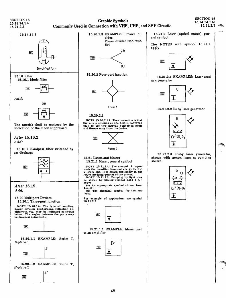
Graphic Symbols SECTION 15 15.14.14.1 to 15.21.2.3 Commonly Used in Connection with VHF, UHF, and SHF Circuits
SECTION 15 15.14.14.1 to
15.21.2.3 ~
15.14.14.1
SImplifIed form
15.16 Filter 15.16.1 Mode filter
Add: OR
The asterisk shall be replaced by the indication of the mode suppressed.
After 15.16.2 Add:
15.16.3 Bandpass filter switched by gas discharge
After 15.19 Add:
15.20 Multiport Devices 15.20.1 Three-port junction NOTE 15.20.1A: The type of coupling.
power division proportions. reflection coefficients. etc. may be indicated as shown below. The angles between the ports may be drawn as convenient.
15.20.1.1 EXAMPLE: Series T, E-plane T
15.20.1.2 EXAMPLE: Shunt T, H-planeT
15.20.1.3 EXAMPLE: Power divider: Power divided into ratio 6:4
15.20.2 Four-port junction
Form 1
15.20.2.1 NOTE 15.20.2.1A: The convention is that
the power entering at one port is conveyed only to the two directly connected ports and thence away from the device.
Form 2
15.21 Lasers and Masers 15.21.1 Maser, general symbol
NOTE 15.21.1A: The symbol I represents the transition from one energy level to a lower one. It is drawn preferably in the lower left-hand quarter of the square.
NOTE 15.21.18: Pumping by light may be shown by placing symbol 1.3.1 ( ",,,, ) above
(a) An appropriate symbol chosen from 1.4. or
(b) The chemical symbol for the material
For example of application. see symbol 15.21.2.2
15.21.1.1 EXAMPLE: Maser used as an amplifier
48
15.21.2 Laser (optical maser), general symbol
The NOTES with symbol 15.21.1 apply.
15.21.2.1 EXAMPLES: Laser used as a generator
15.21.2.2 Ruby laser generator
I 15.21.2.3 Ruby laser generator,
shown with xenon lamp as pumping source
I
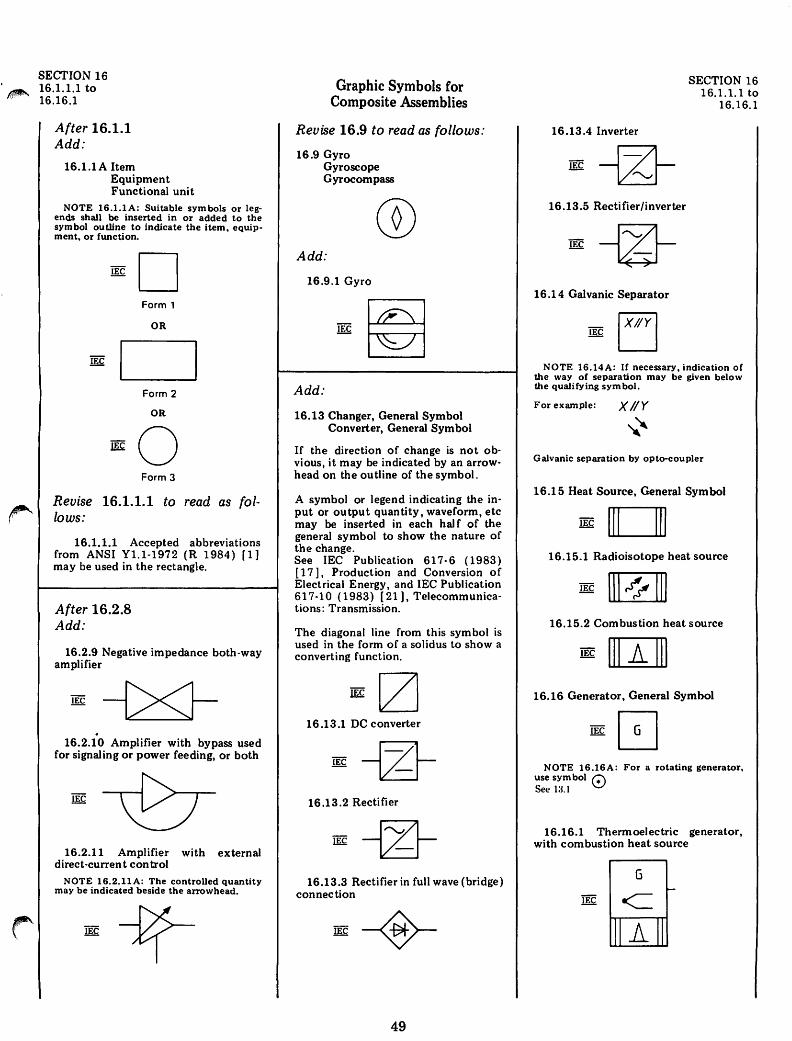
After 16.1.1 Add:
16.1.1 A Item Equipment Functional unit
NOTE 16.1.1A: Suitable symbols or legends shall be inserted in or added to the symbol outline to indicate the item, equipment, or function.
Form 1
OR
Form 2
OR
lEe 0 Form 3
Revise 16.1.1.1 to read as follows:
16.1.1.1 Accepted abbreviations from ANSI Y1.1-1972 (R 1984) [1] may be used in the rectangle.
After 16.2.8 Add:
16.2.9 Negative impedance both-way amplifier
16.2.10 Amplifier with bypass used for signaling or power feeding, or both
16.2.11 Amplifier with external direct-curren t con trol
NOTE 16.2.llA: The controlled quantity may be indicated beside the arrowhead.
Graphic Symbols for Composite Assemblies
Revise 16.9 to read as follows:
16.9 Gyro Gyroscope Gyrocompass
Add:
16.9.1 Gyro
Add:
16.13 Changer, General Symbol Converter, General Symbol
If the direction of change is not obvious, it may be indicated by an arrowhead on the outline of the symbol.
A symbol or legend indicating the input or output quantity, waveform, etc may be inserted in each hal f of the general symbol to show the nature of the change. See IEC Publication 617-6 (1983) [17] I Production and Conversion of Electrical Energy, and IEC Publication 617-10 (1983) [21 J. Telecommunications: Transmission.
The diagonal line from this symbol is used in the form of a solidus to show a converting function.
16.13.1 DC converter
16.13.2 Rectifier
16.13.3 Rectifier in full wave (bridge) connection
49
16.13.4 Inverter
16.13.5 Rectifier/inverter
16.14 Galvanic Separator
SECTION 16 16.1.1.1 to
16.16.1
NOTE 16.14A: If necessary. indication or the way of separation may be given below the qualifying symbol.
For example: x//y
~~
Galvanic separation by opto-coupler
16.15 Heat Source, General Symbol
16.15.1 Radioisotope heat source
16.15.2 Combustion heat source
16.16 Generator, General Symbol
NOTE 16.16A: For a rotating generator, use symbol 0 See I:U
16.16.1 Thermoelectric generator, with combustion heat source
G
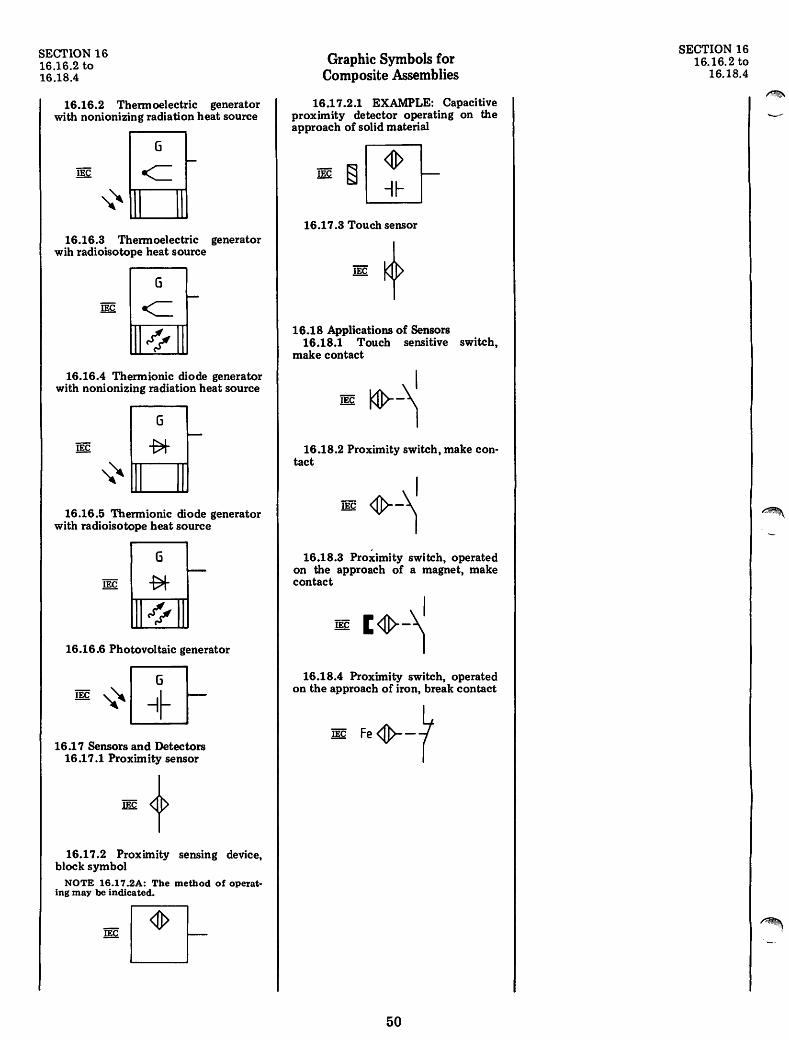
SECTION 16 16.16.2 to 16.18.4
16.16.2 Thennoelectric generator with nonionizing radiation heat source
16.16.3 Thennoelectric generator wih radioisotope heat source
G
16.16.4 Thennionic diode generator with nonionizing radiation heat source
16.16.5 Thennionic diode generator with radioisotope heat source
G
16.16.6 Photovoltaic generator
16.17 Sensors and Detectors 16.17.1 Proximity sensor
16.17.2 Proximity sensing device, block symbol
NOTE 16.17.2A: The method of operating may be indicated.
Graphic Symbols for Composite Assemblies
16.17.2.1 EXAMPLE: Capacitive proximity detector operating on the approach of solid material
16.17.3 Touch sensor
16.18 Applications of Sensors 16.18.1 Touch sensitive switch,
make contact
16.18.2 Proximity switch, make contact
16.18.3 Pro~imity switch, operated on the approach of a magnet, make contact
16.18.4 Proximity switch, operated on the approach of iron, break contact
lEe fe~-t
50
SECTION 16 16.16.2 to
16.18.4
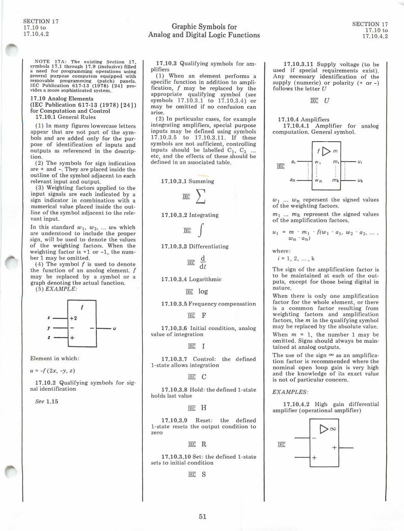
SECTION 17 17.10 to 17.10.4.2
NOTE 17A: The existing Section 17, symbols 17.1 t h rough 1 7.9 (i n clusive) fill ed a need for programming operations u sing ge neral purpose co m puters equi p ped with remo vable progr am m ing (pa t c h ) panels. lEe Publication 6 17-13 ( 1978) r24 ] provides a more sop histicated system.
17.10 Analog Elements (IEC Publicatio n 6 17-13 (19 78) [24 I) fo r Computat ion and Control
17.10.1 General Rules
(1) 111 m any f igures lo wercase letters appear that are not parl of the symbols and are added only for the purpose of identification of inputs and outputs as referenced in the descript io n.
(2) T he symbo ls for sign ind icat ion are + and -. T hey are p laced inside th e out line of the sym bol adjacen t to each relevant input and output.
(3) Weigh ting factors app lied to the input signals are each ind icated by a sign indicator in combination with a numeri ca l value placed inside the o utline of the sym bol adjacent to the relevan t input.
In th is standard WJ, W'l, ... Wn which are understood to inclu de the prope r sign, will be used to denote the values of the weighting factors. When th e weighting factor is + 1 or -I, th e num ber 1 may be o mi tted.
(4) T he symbol r is used to d enote the function of an anolog elem ent. r may be rep laced by a sym bol o r a graph denoting the actual fun ction.
(5) EXAMPLE:
(
z + 2
y u
z +
Element in which:
U = -( (2x , -y, z)
17 .10 .2 Qual ify ing sym bols for signal identificat ion
See 1.1 5
Graphic Symbols for Analog and Digit al Logic Func tions
17.10.3 Qualifying symbols for amplifiers
(1) Wh en an elem ent p erfonn s a specific funct ion in addi t ion to ampli fication, r m ay be replaced by the appropriate q ualify ing sym bol (see sym bols 17 .10.3.1 to 17.10.3.4) or may be om itted if no confusio n can arise.
(2) In pnrt icualar cases. for exam ple integrating amplifiers, special purpose inpu ts may be defi ned using symbols 17.10.3.5 to 17.10.3.11. If these symbols are not sufficient. cont rolli ng inputs should be labelled C 1 • C2 etc, and t he effects of t hese sh o uld be de fined in an assoc iated ta ble.
17 .10 .3.1 Summing
lFoe L 17 .10 .3 .2 Integrat in g
~ f 17.10.3.3 Di ffere ntiating
_ d m; dt
17.1 0 .3.4 Logarithm ic
lEe log
17.10.3. 5 Frequency compensat ion
m; F
17.1 0.3.6 Ini tial condition, analog va lue o f integration
lEG I
17.10.3.7 Control: the defined l·state allows integrat io n
[Ee C
17 .10.3 .8 Hold: t he defined I-state holds last value
[FoG H
17.10.3 .9 Reset: t he defined I-state resets the o utput cond it ion to zero
l Ee R
17.10.3 .10 Set: t he de fin ed 1·state sets lo initial condition
lEe S
51
SECTION 17 17 .10 to
17 .10.4.2
17.10.3 .11 Supply voltage (to be used if specia l requ irements exist). A n y necessary iden l ifica t ion of the suppl y ( numeric ) or po la ri ly (+ or -) follows the lette r U
lEG U
17.10.4 Am p lifiers 17.10.4 .1 A mplifier for analog
computation. General sym bol.
a, m, u ,
an Uk
WI ... wn repersenl the signed va lues of the w e igh ti ng facto rs.
mi... m k rep resent th e signed values of the amplificatio n factors.
III = m . mI' r(w I . a I , W'l . a2.
Wn . an'
where: i=1,2, ... ,k
The sign of lhe amplifical ion factor is to be maintained at each of the oul· puts. excep t for those being digita l in nalure.
When th ere is only one amplification factor fo r the who le e lement, or th ere is a comm on factor resulling from weightin g factors and amplification facto rs, lhe m in lh e qu ali fy ing symbol m ay be replaced by the absol ule value.
When m = 1. the number 1 may be o m itted . S igns shou ld a lways be maintained at analog o u tpu ts.
The use of lhe sign to:) as an amplifical io n factor is recommended where t he nomin al open loop ga in is very high and lh e knowledge of ils exact value is not of particular concern .
EXAMPLES:
17.10.4.2 High ga in d ifferential ampl i fi er (operat iona l am p lifier)
+ +
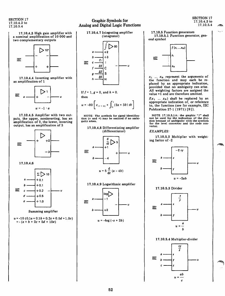
SECTION 17 17.10.4.3 to 17.10.5.4
17.10.4.3 High gain amplifier with a nominal amplification of 10 000 and two complementary outputs
+ +
17.10.4.4 Inverting amplifier with an amplification of 1
a + u
u:::: -1 . 0
17.10.4.5 Amplifier with two outputs, the upper, noninverting, has an amplification of 2, the lower, inverting output, has an amplification of 3
t> +
17.10.4.6
L [> 10
a +0.1
b +0.1 lEe c +0.2 u
d +0.5
e + 1.0
Summing amplifier
u = -10 (0.10 + 0.1b + 0.2c + 0.5d + 1.0c) ; - (0 + b + 2c + 5d + 10e)
Graphic Symbols for Analog and Digital Logic Functions
17.10.4.7 Integrating amplifier (integrator)
J[>80 a +2
b +3
lEe c
f C
9 5
h H
If (= 1,g= 0, and h:;: O.
then
u
u = -80 [C(f ~ 0) + fIt (20 + 3b) dt]
NOTE: The symbols for signal identification (n and :) may be omitted if no ambiguity arises.
17.10.4.8 Differentiating amplifier ( differentiator)
d dt [> 5
a +1 lEe + u
b --4
d u = 5 - (0 - 4b)
dt
17.10.4.9 Logarithmic amplifier
109[> a -1
lEe u
b +2
u = -log (-a + 2b)
52
SECTION 17 17.10.4.3 to
17.10.5.4 ~
17.10.5 Function generators 17.10.5.1 Function generator, gen
eral symbol
f (x, ... xn)
Xl .. ' Xn represent the arguments of the function and may each be replaced by an appropriate indication, provided that no ambiguity can arise. All weighting factors are assigned the value +1 and are therefore omitted. {(Xl'" Xn) shall be replaced by an appropriate indication of, or reference to, the function (see for example, IEC Publication 27-1 (1971) [9]).
NOTE 17.10.5.1A: the graphic .. ," shall not be used for the indication of the division because of ambiguity with the symbols for the level converter and the code converter.
EXAMPLES:
17.10.5.2 Multiplier with weighting factor of-2
-2 xy
a x
b y
u = -20b
17.10.5.3 Divider
a x
b y
x y
o u =-
b
u
u
17.10.5.4 Multiplier-divider
a x IE b y
c z
xy
z
ob u=-
C
u
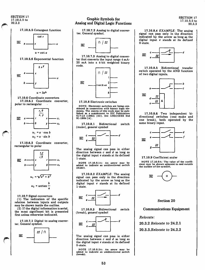
SECTION 17 17.10.5.5 to 20.3.3
17.10.5.5 Cotangent function
cot x
x u
U'" cot a
17.10.5.6 Exponential function
3 xy
u
b Y
u'" 3ab
17.10.6 Coordinate converters 17.10.6.1 Coordinate converter,
polar to rectangular
lEe a
b
, IJ
" (} X,Y
x
Y
Ul = a' cos b U2 = a . sin b
17.10.6.2 Coordinate converter, rectangular to polar
lEe a
b
X,Y
,,8 x
Y 0
b u2 = arctan
a
17.10.7 Signal convertors
u,
U2
( 1) The indication of the specific relation between inputs and outputs may be shown inside the outline.
(2) If the digital information is serial, the most significant bit is presented first unless otherwise indicated.
17.10.7.1 Digital to analog converter. General symbol.
Graphic Symbols for Analog and Digital Logic Functions
17.10.7.2 Analog to digital converter. General symbol.
n l:t:t
17.10.7.3 Analog to digital converter that converts the input range 4 mA-20 mA into a 4·bit weighted binary code.
n I tt
4 rnA·20 rnA 2
4
8
17.10.8 Electronic switches NOTE: Electronic switches are being con
sidered in connection with binary logic elements. The results of this work may be published as a supplement to lEe Publciation 617·12 (1983) [231. See ANSI/IEEE Std 91·1984 [4].
17.10.8.1 Bidirectional switch (make), general symbol
c ..-/- d
e tt
The analog signal can pass in either direction between c and d as long as the digital input e stands at its defined I-state.
NOTE 17.10.8.1A: An arrow may be added to indicate an unidirectional switch (make).
17.10.8.2 EXAMPLE: The analog signal can pass only in the direction indicated by the arrow as long as the digital input e stands at its defined t·state.
c
e
17.10.8.3 Bidirectional (break), general symbol
d
C~d IECe~
switch
The analog signal can pass in either direction between c and d as long as the digital input e stands at its defined O-state.
NOTE 17.10.8.3A: An arrow may be added to indicate an unidirectional switch (break).
53
SECTION 17 17.10.5.5 to
20.3.3
17.10.8.4 EXAMPLE: The analog signal can pass only in the direction indicated by the arrow as long as the digital input e stands at its defined O-state.
17.10.8.5 Bidirectional transfer switch operated by the AND function of two digital i~puts.
b
a C
d
e
17.10.8.6 Two independent bidirectional switches (one make and one break), both operated by the same binary input.
c ~-e ~
lEe
9
17.10.9 Coefficient scaler
d
f
NOTE 17.10.9A: The value of the coefficient may be shown adjacent to and outside the outline of the symbol.
Section 20
Communications Equipment
Relocate:
20.3.2 Relocate to 24.2.1
20.3.3.Relocate to 24.2.2
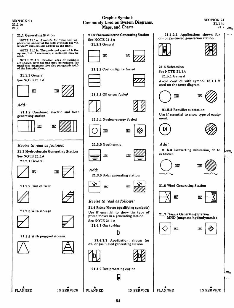
SECTION 21 21.1 to 21.7
21.1 Generating Station NOTE 2l.1A: Symbols for "planned" ap
plications appear at the left: symbols for "in service" applicatiuns appear at the right.
NOTE 2l.18: The preferred symbol is the square. but if necessary. a rectangle may be used.
NOTE 2l.1C: Relative sizes of symbols are shown. Symbol size may be reduced for small-size diagrams. See also paragraph A4.5 of the Introduction.
21.1.1 General See NOTE 21.1A
Add:
21.1.2 Combined electric and heat generating station em lEe lEe
Revise to read as follows:
21.2 Hydroelectric Generating Station See NOTE 21.1A
21.2.1 General
21.2.2 Run of river
21.2.3 With storage
21.2.4 With pumped storage
• PLANNED • IN SERVICE
Graphic Symbols Commonly Used on System Diagrams,
Maps, and Charts
21.3 Thermoelectric Generating Station See NOTE 21.1A
21.3.1 General
21.3.2 Coal or lignite fueled
21.3.3 Oil or gas fuele~
21.3.4 Nuclear-energy fueled
21.3.5 Geothermic
Add: 21.3.6 Solar generating station
Revise to read as follows:
21.4 Prime Mover (qualifying symbols) Use if essential to show the type of prime mover in a generating station. See NOTE 21.1A
21.4.1 Gas turbine
D 21.4.1.1 Application: shown for
oil- or gas-fueled generating station
21.4.2 Reciprocating engine
• PLANNED
54
• IN SERVICE
SECTION 21 21.1 to
21.7 ~
21.4.2.1 Application: shown for oil- or gas-fueled generation station
21.5 Substation See NOTE 21.1A
21.5.1 General Avoid conflict with symbol 13.1.1 if used on the same diagram. o lEe
21.5.2 Rectifier substation Use if essential to show type of equipment.
Add: 21.5.3 Converting SUbstation, dc to
ac shown
Omc -/""'-' -/~
21.6 Wind Generating Station
21.7 Plasma Generating Station MHD (magneto-hydrodynamic)
• PLANNED • IN SERVICE
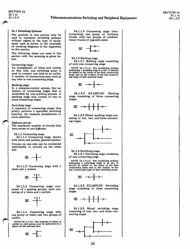
SECTION 24 24.1 to 24.1.3.3 Telecommunications Switching and Peripheral Equipment
~c , I
24.1 Switching Systems The symbols in this section may be used to represent switching systems without regard to the type of equipment used as shown in the examples of trunking diagrams in the Appendix to this section. The following terms are used in this section with the meaning as given below.
Connecting stage: An arrangement of inlets and outlets so that only one switching point is used to connect one inlet to an outlet. A number of connections may exist at any time in one connecting stage.
Mark ing stage: In a common-control system, that sequence of connecting stages that is controlled by one marking process. A marking stage may consist of one or more connecting stages.
Switching stage: A sequence of connecting stages that jointly perform a specified switching function, for example preselection or route selection.
Highway-group: The maximum number of circuits that have access to one highway.
24.1.1 Connecting stage 24.1.1.1 Connecting stage, shown
with inlets and outlets, general symbol
Circuits on one side can be connected individually to circuits on the other side
IEC + 24.1.1.2 Connecting stage with x
inlets and y outlets
24.1.1.3 Connecting stage composed of z grading groups, each consisting of x inlets and y outlets
24.1.1.4 Connecting stage with one group of inlets and two groups of outlets
NOTE 24.1.1.4A: The number of inlets or outlets in each group may be indicated by a figure on the relevant line.
24.1.1.5 Connecting stage interconnecting one group of both way trunks with two groups of unidirectional trunks of opposite sense
24.1.2 Marking stage 24.1.2.1 Marking stage consisting
of only one connecting stage NOTE 24.1.2.1A: The qualifying symbol
indicating a marking stage is a dot. It should be added to the inlets of the first connecting stage and to the outlets of the last connecting stage of that marking stage.
• •
24.1.2.2 EXAMPLES: Marking stage consisting of three connecting stages
IEC • I I I · 24.1.2.3 Mixed marking stage con
sisting of one, two, and three connecting stages
I _ I
-
24.1.3 Switching stage 24.1.3.1 Switching stage consisting
of one connecting stage NOTE 24.1.3.1A: The qualifying symbol
indicating a switching stage is an arc. It should be added to the inlets of the first connecting stage and to the outlets of the last connecting stage of that switching stage.
( )
24.1.3.2 EXAMPLES: Switching stage consisting of three connecting stages
24.1.3.3 Mixed switching stage consisting of one, two, and three connecting stages
55
SECTION 24 24.1 to
24.1.3.3
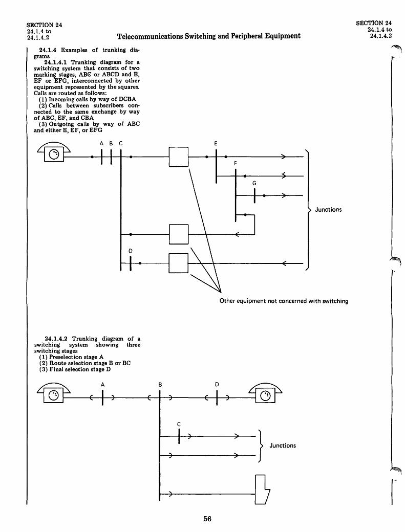
SECTION 24 24.1.4 to 24.1.4.2 Telecommunications Switching and Peripheral Equipment
24.1.4 Examples of trunking diagrams
24.1.4.1 Trunking diagram for a switching system that consists of two marking stages, ABe or ABCD and E, EF or EFG, interconnected by other equipment represented by the squares. Calls are routed as fonows:
(1) Incoming calls by way of DCBA (2) Calls between subscribers con
nected to the same exchange by way of ABC, EF, and CBA
(3) Outgoing calls by way of ABC and either E, EF, or EFG
o
24.1.4.2 Trunking diagram of a switching system showing three switching stages
(1) Preselection stage A (2) Route selection stage B or BC ( 3) Final selection stage D
E
G
Junctions
Other equipment not concerned with switching
c
t---+--------~--} Junctions
56
SECTION 24 24.1.4 to 24.1.4.2
SECTION 24 24.2 to
~24.4.4 Telecommunications Switching and Peripheral Equipment
24.2 Block Symbols for Switching Equipment
24.2.1 Automatic switching*
*Relocated tram 20.3.2
24.2.2 Manual switchboard*
*Relocated from 20.3.3
24.3 Qualifying Symbols for Transducers, Recorders, and Reproducers
24.3.1 Magnetic type
~ J 24.3.2 Moving coil or ribbon type
lEe IY"'\
24.3.3 Moving iron type
lEe IY"'\
24.3.4 Stereo type
24.3.5 Disc type
!f&(1 24.3.6 Tape or film type
~OD
24.3.7 Drum type
m LJ 24.3.8 Recording or reproducing
(the arrow points in the direction of energy transfer)
lE£ ---.
24.3.9 Recording and reproducing
.IE ..
24.3.10 Erasing
lEe X
24.4 Recorders and Reproducers 24.4.1 Recorder or reproducer, or
both, general symbol NOTE 24.4.1A: The qualifying symbol
depicting a transducer head may be replaced by other qualifying symbols.
24.4.1.1 EXAMPLE: Recorder and reproducer, magnetic drum type
24.4.2 Reproducer with a stylus operated head
24.4.3 Recorder, film-type, with a head producing modulated light
-
24.4.4 Reproducer, disc-type, with a light-operated head
57
SECTION 24 24.2 to 24.4.4
SECTION 25 25.1 to 25.4.7
25.1 Amplified Circuits 25.1.1 Two-wire line with unidirec
tional amplification
25.1.2 Two-wire line with both-way amplification
lK ---If4><}--#-25.1.3 Four-wire circuit with both
way amplification
IEC~ Form 1
OR
Form 2
25.1.4 Four-wire type circuit with frequency separation
f.t ... f2
25.1.5 Four-wire circuit with bothway terminal amplification with echo suppression
4 4 I [><J I. ;
t I
Form 1
OR
tt [>--#-<l lSI. I
Form 2
25.2 Qualifying Symbols for Pulse Modulation
25.2.1 Pulse-position or pulse-phase modulatiojl
IEC n 25.2.2 Pulse-frequency modulation
Telecommunications Transmission
25.2.3 Pulse-amplitude modulation
IEC A 25.2.4 PUlse-interval modulation
25.2.5 Pulse-duration modulation
IEC ~
25.2.6 Pulse-code modulation NOTE 25.2.6A: The * must be replaced
by details of the code.
- n* ~ .J L
25.2.6.1 EXAMPLE: 3-out-of-7 code
25.3 Signal Generator Wavefonn Generator
25.3.1 Sine-wave generator, 500 Hz
25.3.2 Sawtooth generator, 500 Hz
IEC I~~ 500 Hz
25.3.3 Pulse generator
25.3.4 Variable frequency sine-wave generator
58
SECTION 25 25.1 to 25.4.7 ~
25.3.5 Noise generator k = Boltzmann's constant T = absolute temperature
-1Gl.m£~
25.4 Changers Converter, General Symbol
25.4.1 Frequency changer, changing from {I to {2
IEC~ 25.4.2 Frequency multiplier
- --@-lEe - nf
25.4.3 Frequency divider
25.4.4 Pulse inverter
25.4.5 Code converter, five-unit binary code to seven-unit binary code
25.4.6 Changer giving clock-time indication in five-unit binary code
25.4.7 Pulse regenerator
iEc~ -1LB:j
r
SECTION 25 25.5 to
,.., 25.8.2
25.5 Filters 25.5.1 Filter, general symbol
25.5.2 High-pass filter
25.5.3 Low-pass filter
25.5.4 Band-pass filter
25.5.5 Band-stop filter
r" 25.6 Networks I.~,
25.6.1 Device for pre-emphasis higher frequencies
lEe -B-25.6.2 Device for de-emphasis
higher frequencies
lEe --B-25.6.3 Compressor
lEe -§-25.6.4 Expander
lEe --g]-25.6.5 Artificial line
~ -[D-r
of
of
Telecommunications Transmission
25.6.6 Phase-changing network
NOTE: t() may be replaced by B if no confusion arises
*Coordinate with symbol 15.17
25.6.7 Distortion corrector, general symbol
25.6.8 Amplitude/frequency distortion corrector, for example, equalizer
25.6.9 Phase/frequency distortion corrector
NOTE 25.6.9A: If it is desirable to indicate that the equalization refers to the time derivative of t(). t() may be replaced by <1».
25.6.10 Delay/frequency distortion corrector
25.6.11 Nondistorting amplitude controller
25.6.12 Mixing network
25.7 Electronic Chopping Device
IEc~ -~
59
25.8 Threshold Devices
SECTION 25 25.5 to 25.8.2
There are two ways of showing details of the operation carried out by a threshold device. The first is the llse of the symbol 25.8.1 supplemented by appropriate waveform symbols on the input and output lines. The second is the use of a specific symbol consisting of a rectangle containing a figure derived from the input/output characteristic in the following manner:
The axes are deleted, but the origin is indicated by a short vertical stroke representing the y-axis
EXAMPLE:
Output
Characteristic: =f Input
Symbol:
The origin may be located in the rec· tangle in such a position that the characteristic makes the maximum use of the available space
EXAMPLE:
Output
Characteristic: + Input
Symbol:
25.8.1 Threshold device, type un· specified (for example clipper)
25.8.2 Device having a linear input/ output characteristic for all signals that exceed a given threshold value and which has no output for input sig· nals having an instantaneous amplitude between zero and that threshold
SECTION 25 25.8.3 to 25.11.8
25.8.3 Device having a linear input/ output characteristic for all signals that exceed a preset threshold value and that has no output for input signals having an instantaneous amplitude between zero and that threshold
25.8.4 Positive peak clipper
25.8.5 Negative peak clipper
25.9 Terminating Sets 25.9.1 Terminating set
25.9.2 Balancing network
25.9.3 Terminating set with balal1-cing network
25.9.4 Hybrid transfonner
25.9.5 Asymmetric (skew) hybrid transformer, shown with balancing network
Telecommunications Transmission
25.9.6 Equipment for connecting a four-wire circuit to either a two-wire circuit or a four-wire circuit depending upon the reception of a control signal
25.10 Modulator Demodulator Discrim inator
25.10.1 General symbol
NOTE 25.10.1A: This symbol is used as follows: (Letters and ir.put and output lines have been added in the figure for the purpose of explanation.)
a and b represent the modulating or modulated signal input and the modulated or demodulated signal output
c represents the input of the carrier-wave if required
Qualifying symbols may be placed inside or outside the symbol as shown below
25.10.1.1 Modulator, double sideband output
25.10.1.2 Pulse code modulator (seven-unit binary code output)
G
JL
25.10.2 Demodulator, single sideband with suppressed carrier to audio
...
m£ ~~
60
25.11 Concentrators Multiplexers
SECTION 25 25.8.3 to
25.11.8
25.11.1 Concentrating switching function from left to right, qualifying symbol
25.11.2 Expanding switching function from left to right, qualifying symbol
25.11.3 EXAMPLES: Concentrator with m input circuits and n output circuits
D IEC m
Form 1
Form 2
I \ n I
25.11.4 Multiplexing function, qualifying symbol
iEC MUX
25.11.5 Demultiplexing function, qualifying symbol
NOTE 25.11.5A: If confusion can arise, DX may be replaced by DMUX.
~ OX
25.11.6 Multiplexing and demultiplexing function, qualifying sym hoI
IEC MULOEX
25.11.7 Multiplexer with analog/ digital conversion
25.11.8 Multiplexer/demultiplexer with analog/digital conversion
MULDEX
n/#
SECTION 25 25.12 to 25.13.2
25.12 Frequency Spectrum Diagram Symbol Elements A frequency spectrum is represented on a diagram by means of symbols on a horizontal frequency axis. The symbols show the functions of the various frequencies and frequency bands used in the transm ission system as well as their relative positions in the spectrum.
25.12.1 Carrier frequency NOTE 25.12.1A: When this symbol is
used to represent a carrier that is modulated in frequency or phase the f or o.p is added. See. for example. symbol 25.13.2.
NOTE 25.12.18: The arrowhead on the vertical line representing the carrier (and the arrowhead on the frequency axis) may be omitted if no confusion will result.
IEC~ f
25.12.1.1 Suppressed-carrier frequency
25.12.1.2 quency
!l\ I I I I
f
Reduced-carrier
I I
t 25.12.2 Pilot frequency
fre-
NOTE 25.12.2A: For FDM transmission systems the order of the group to which the pilot refers. that is. grouP. supergroup. mastergroup. or supermastergroup may be indicated by adding the respective number 1.2.3. or.4 of oblique strokes.
IEC~ f
EXAMPLE: Supergroup pilot frequency
25.12.2.1
f
25.12.2.2 Suppressed pilot frequency
~ I I I I
Telecommunications Transmission
25.12.3 Additional measuring frequency
25.12.3.1 Additional measuring frequency, transmitted or measured on request
25.12.4 Signaling frequency
mc-L 25.12.5 Frequency band NOTE 25.12.5A: If it is desired to show
whether a Particular band of frequencies is erect or inverted. symbol 25.12.6 or 25.12.7 should be used.
NOTE 25.12.58: The order of a band of frequencies forming part of a transmission system may be indicated by adding oblique strokes according to NOTE 25.12.2A of symbol 25.12.2.
,. 25.12.5.1 EXAMPLE: Mastergroup
NOTE 25.12.5.1A: The division of a band into channels. groups. etc. may be shown by adding vertical lines.
25.12.5.2 EXAMPLE: Band of frequencies from fl to '2 divided into five channels, groups, etc.
IEC I I I I I I . f, I, I
61
SECTION 25 25.12 to 25.13.2
25.12.6 Erect band of frequencies NOTE 25.12.6A: There is no indication of
how much of the bandwidth shown by the symbol is actually used.
NOTE 25.12.68: This symbol may be used to represent a single channel. grouP. etc. or a number of channels. groups. etc. providing they are all erect.
25.12.6.1 EXAMPLE: Band of frequencies consisting of a group of 12 erect channels
lEC AAAAAAAAAAAA fYYVVYVVVYW •
f
25.12.6.2
~ ~. f
Simplified form
25.12.7 Inverted band of frequencies NOTES 25.12.6A and 25.12.6B apply.
25.12.8 Band of mixed channels, groups, etc, some erect, remainder inverted
lE r><1 • f
25.13 Examples of Frequency Spectrum Diagrams
25.13.1 Amplitude'modulated carrier with both sidebands
25.13.2 Phase modulated carrier with both sidebands
NOTE 25.13.2A: For frequency modulation. replace o.p with f.
SECTION 25 25.13.3 to 25.14.2
25.13.3 Amplitude-modulated carrier with both sidebands, lower modulating frequencies not being transmitted
25.13.4 Amplitude-modulated carrier with both sidebands, modulating frequencies down to zero being transmitted
25.13.5 Single-sideband suppressed carrier
25.13.6 Reduced-carrier with single, lower, erect sideband
25.13_7 Suppressed-carrier with single-sideband scrambled for secrecy
25_13.8 Amplitude-modulated carrier with upper sideband and lower vestigial sideband, modulating frequencies down to zero being transmitted
25.13.9 Band of five channels, groups, etc, four of which are inverted and one erect
t\!t\N\ . f
Telecommunications Transmission
25.13.10 4 MHz transmission system showing supergroups and pilot frequencies
CD
~
~ ~ 1 2 3
,I"--'--II~II IIII1II1III ~~ oJ" oJ"
25.14 Fiber Optic Devices 25.14.1 Guided light transmitter
25.14.2 Guided light receiver
62
SECTION 25 25.13.3 to
25.14.2
N 0-o ~
15 16 ~ I I I I I I I I I I I II