Subscriber access provided by UNIV OF CAMBRIDGE ... · Fazio, Giancarlo Soavi, Ugo Sassi, Federico...
44
Subscriber access provided by UNIV OF CAMBRIDGE is published by the American Chemical Society. 1155 Sixteenth Street N.W., Washington, DC 20036 Published by American Chemical Society. Copyright © American Chemical Society. However, no copyright claim is made to original U.S. Government works, or works produced by employees of any Commonwealth realm Crown government in the course of their duties. Communication
-
Upload
nguyendung -
Category
Documents
-
view
212 -
download
0
Transcript of Subscriber access provided by UNIV OF CAMBRIDGE ... · Fazio, Giancarlo Soavi, Ugo Sassi, Federico...
Subscriber access provided by UNIV OF CAMBRIDGE
is published by the American Chemical Society. 1155 Sixteenth Street N.W.,Washington, DC 20036Published by American Chemical Society. Copyright © American ChemicalSociety. However, no copyright claim is made to original U.S. Governmentworks, or works produced by employees of any Commonwealth realm Crowngovernment in the course of their duties.
Communication
Subscriber access provided by UNIV OF CAMBRIDGE
is published by the American Chemical Society. 1155 Sixteenth Street N.W.,Washington, DC 20036Published by American Chemical Society. Copyright © American ChemicalSociety. However, no copyright claim is made to original U.S. Governmentworks, or works produced by employees of any Commonwealth realm Crowngovernment in the course of their duties.
Intravalley Spin-Flip Relaxation Dynamics In Single-Layer WS<u>2</u>
Subscriber access provided by UNIV OF CAMBRIDGE
is published by the American Chemical Society. 1155 Sixteenth Street N.W.,Washington, DC 20036Published by American Chemical Society. Copyright © American ChemicalSociety. However, no copyright claim is made to original U.S. Governmentworks, or works produced by employees of any Commonwealth realm Crowngovernment in the course of their duties.
Zilong Wang, Alejandro Molina-Sánchez, Patrick Altmann, Davide Sangalli, Domenico DeFazio, Giancarlo Soavi, Ugo Sassi, Federico Bottegoni, Franco Ciccacci, Marco Finazzi,
Ludger Wirtz, Andrea C Ferrari, Andrea Marini, Giulio Cerullo, and Stefano Dal Conte
Subscriber access provided by UNIV OF CAMBRIDGE
is published by the American Chemical Society. 1155 Sixteenth Street N.W.,Washington, DC 20036Published by American Chemical Society. Copyright © American ChemicalSociety. However, no copyright claim is made to original U.S. Governmentworks, or works produced by employees of any Commonwealth realm Crowngovernment in the course of their duties.
Nano Lett., Just Accepted Manuscript • DOI: 10.1021/acs.nanolett.8b02774 • Publication Date (Web): 28 Sep 2018
Subscriber access provided by UNIV OF CAMBRIDGE
is published by the American Chemical Society. 1155 Sixteenth Street N.W.,Washington, DC 20036Published by American Chemical Society. Copyright © American ChemicalSociety. However, no copyright claim is made to original U.S. Governmentworks, or works produced by employees of any Commonwealth realm Crowngovernment in the course of their duties.
Downloaded from http://pubs.acs.org on October 3, 2018
Subscriber access provided by UNIV OF CAMBRIDGE
is published by the American Chemical Society. 1155 Sixteenth Street N.W.,Washington, DC 20036Published by American Chemical Society. Copyright © American ChemicalSociety. However, no copyright claim is made to original U.S. Governmentworks, or works produced by employees of any Commonwealth realm Crowngovernment in the course of their duties.
Just Accepted

Subscriber access provided by UNIV OF CAMBRIDGE
is published by the American Chemical Society. 1155 Sixteenth Street N.W.,Washington, DC 20036Published by American Chemical Society. Copyright © American ChemicalSociety. However, no copyright claim is made to original U.S. Governmentworks, or works produced by employees of any Commonwealth realm Crowngovernment in the course of their duties.
“Just Accepted” manuscripts have been peer-reviewed and accepted for publication. They are postedonline prior to technical editing, formatting for publication and author proofing. The American Chemical

Subscriber access provided by UNIV OF CAMBRIDGE
is published by the American Chemical Society. 1155 Sixteenth Street N.W.,Washington, DC 20036Published by American Chemical Society. Copyright © American ChemicalSociety. However, no copyright claim is made to original U.S. Governmentworks, or works produced by employees of any Commonwealth realm Crowngovernment in the course of their duties.
Society provides “Just Accepted” as a service to the research community to expedite the dissemination
Subscriber access provided by UNIV OF CAMBRIDGE
is published by the American Chemical Society. 1155 Sixteenth Street N.W.,Washington, DC 20036Published by American Chemical Society. Copyright © American ChemicalSociety. However, no copyright claim is made to original U.S. Governmentworks, or works produced by employees of any Commonwealth realm Crowngovernment in the course of their duties.
of scientific material as soon as possible after acceptance. “Just Accepted” manuscripts appear in
Subscriber access provided by UNIV OF CAMBRIDGE
is published by the American Chemical Society. 1155 Sixteenth Street N.W.,Washington, DC 20036Published by American Chemical Society. Copyright © American ChemicalSociety. However, no copyright claim is made to original U.S. Governmentworks, or works produced by employees of any Commonwealth realm Crowngovernment in the course of their duties.
full in PDF format accompanied by an HTML abstract. “Just Accepted” manuscripts have been fully

Subscriber access provided by UNIV OF CAMBRIDGE
is published by the American Chemical Society. 1155 Sixteenth Street N.W.,Washington, DC 20036Published by American Chemical Society. Copyright © American ChemicalSociety. However, no copyright claim is made to original U.S. Governmentworks, or works produced by employees of any Commonwealth realm Crowngovernment in the course of their duties.
peer reviewed, but should not be considered the official version of record. They are citable by the

Subscriber access provided by UNIV OF CAMBRIDGE
is published by the American Chemical Society. 1155 Sixteenth Street N.W.,Washington, DC 20036Published by American Chemical Society. Copyright © American ChemicalSociety. However, no copyright claim is made to original U.S. Governmentworks, or works produced by employees of any Commonwealth realm Crowngovernment in the course of their duties.
Digital Object Identifier (DOI®). “Just Accepted” is an optional service offered to authors. Therefore,

Subscriber access provided by UNIV OF CAMBRIDGE
is published by the American Chemical Society. 1155 Sixteenth Street N.W.,Washington, DC 20036Published by American Chemical Society. Copyright © American ChemicalSociety. However, no copyright claim is made to original U.S. Governmentworks, or works produced by employees of any Commonwealth realm Crowngovernment in the course of their duties.
the “Just Accepted” Web site may not include all articles that will be published in the journal. After

Subscriber access provided by UNIV OF CAMBRIDGE
is published by the American Chemical Society. 1155 Sixteenth Street N.W.,Washington, DC 20036Published by American Chemical Society. Copyright © American ChemicalSociety. However, no copyright claim is made to original U.S. Governmentworks, or works produced by employees of any Commonwealth realm Crowngovernment in the course of their duties.
a manuscript is technically edited and formatted, it will be removed from the “Just Accepted” Web

Subscriber access provided by UNIV OF CAMBRIDGE
is published by the American Chemical Society. 1155 Sixteenth Street N.W.,Washington, DC 20036Published by American Chemical Society. Copyright © American ChemicalSociety. However, no copyright claim is made to original U.S. Governmentworks, or works produced by employees of any Commonwealth realm Crowngovernment in the course of their duties.
site and published as an ASAP article. Note that technical editing may introduce minor changes

Subscriber access provided by UNIV OF CAMBRIDGE
is published by the American Chemical Society. 1155 Sixteenth Street N.W.,Washington, DC 20036Published by American Chemical Society. Copyright © American ChemicalSociety. However, no copyright claim is made to original U.S. Governmentworks, or works produced by employees of any Commonwealth realm Crowngovernment in the course of their duties.
to the manuscript text and/or graphics which could affect content, and all legal disclaimers and
Subscriber access provided by UNIV OF CAMBRIDGE
is published by the American Chemical Society. 1155 Sixteenth Street N.W.,Washington, DC 20036Published by American Chemical Society. Copyright © American ChemicalSociety. However, no copyright claim is made to original U.S. Governmentworks, or works produced by employees of any Commonwealth realm Crowngovernment in the course of their duties.
ethical guidelines that apply to the journal pertain. ACS cannot be held responsible for errors orconsequences arising from the use of information contained in these “Just Accepted” manuscripts.
0.40.20.0-0.2delay (ps)
PUMPPROBE
1L-WS2
τspin-flip
∆T/T
Page 1 of 27
ACS Paragon Plus Environment
Nano Letters
123456789101112131415161718192021222324252627282930313233343536373839404142434445464748495051525354555657585960
Intravalley Spin-Flip Relaxation Dynamics In
Single-Layer WS2
Zilong Wang,† Alejandro Molina-Sánchez,‡ Patrick Altmann,† Davide Sangalli,¶
Domenico De Fazio,§ Giancarlo Soavi,§ Ugo Sassi,§ Federico Bottegoni,† Franco
Ciccacci,† Marco Finazzi,† Ludger Wirtz,∥ Andrea C. Ferrari,∗,§ Andrea Marini,¶
Giulio Cerullo,†,⊥ and Stefano Dal Conte†
Department of Physics, Politecnico di Milano, Piazza Leonardo da Vinci 32, I-20133 Milano,
Italy, Institute of Materials Science (ICMUV), University of Valencia, Catedrático Beltrán 2,
E-46980, Valencia, Spain, CNR-ISM, Division of Ultrafast Process in Materials (FLASHit), Area
della Ricerca di Roma 1, Monterotondo Scalo, Italy, Cambridge Graphene Centre, University of
Cambridge, 9 JJ Thomson Avenue, Cambridge CB3 0FA, UK, Université du Luxembourg, 162 A,
avenue de la Faencerie, L-1511 Luxembourg, and IFN-CNR, Piazza Leonardo da Vinci 32,
I-20133 Milano, Italy
E-mail: [email protected]
Phone: +44-1223-748351. Fax: +44-1223-748348
Abstract∗To whom correspondence should be addressed†Politecnico di Milano‡University of Valencia¶CNR-ISM§Cambridge Graphene Centre∥Université du Luxembourg⊥IFN-CNR
1
Page 2 of 27
ACS Paragon Plus Environment
Nano Letters
123456789101112131415161718192021222324252627282930313233343536373839404142434445464748495051525354555657585960
In monolayer (1L) Transition Metal Dichalcogenides (TMDs) the valence and conduction
bands are spin-split because of the strong spin-orbit interaction. In tungsten-based TMDs the
spin-ordering of the conduction band is such that the so-called dark excitons, consisting of
electrons and holes with opposite spin orientation, have lower energy than A excitons. The
transition from bright to dark excitons involves the scattering of electrons from the upper to
the lower conduction band at the K point of the Brillouin Zone, with detrimental effects for
the optoelectronic response of 1L-TMDs, since this reduces their light emission efficiency.
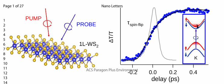
Here we exploit the valley selective optical selection rules and use two-color helicity-resolved
pump-probe spectroscopy to directly measure the intravalley spin-flip relaxation dynamics in
1L-WS2. This occurs on a sub-ps time scale and it is significantly dependent on tempera-
ture, indicative of phonon-assisted relaxation. Time-dependent ab-initio calculations show that
intra-valley spin-flip scattering occurs on significantly longer time scales only at the K point,
while the occupation of states away from the minimum of the conduction band significantly
reduces the scattering time. Our results shed light on the scattering processes limiting the light
emission efficiency in optoelectronic and photonic devices based on 1L-TMDs.
keywords: transition metal dichalcogenides; transient absorption spectroscopy; spin and valley
dynamics; layered materials, optoelectronics
2
Page 3 of 27
ACS Paragon Plus Environment
Nano Letters
123456789101112131415161718192021222324252627282930313233343536373839404142434445464748495051525354555657585960
Transition metal dichalcogenides (TMDs) are promising for opto-electronics,1–4 valleytron-
ics5–9 and quantum information processing.10 TMD monolayers (1L) are direct bandgap semicon-
ductors,11 with optical properties dominated by excitons with binding energies of up to several
hundred meVs.12–18 The valence/conduction (VB/CB) band extrema lie at the non-equivalent K
and K’ points on the edge of the Brillouin zone.19,20 Their spin-degeneracy is lifted by strong spin-
orbit (SO) interaction.21 For the VB, the energy splitting ∆v is between 150 and 400meV,22 while
for the CB ∆c it is one/two orders of magnitude lower (∼1-30meV).23,24 Together with a bro-
ken inversion symmetry, this results in spin-polarized bands and valley-dependent dipole-allowed
interband optical transitions, as first detected by helicity resolved photoluminescence (PL).25–27
The large VB splitting gives rise to two distinct interband transitions (called A and B) strongly
renormalized by excitonic effects,16 dominating the optical response in the visible range.22
Refs. 28–33 predicted that, while the spin orientation of the upper and lower CB states is
antiparallel in K/K’, in W-based 1L-TMDs, the upper CB has the same spin orientation as the
upper VB. A direct consequence of this spin-ordering is the formation of an intravalley (i.e. zero
momentum) dark exciton with a lower energy than the bright exciton. The bright to dark exciton
transition reduces the PL quantum yield in W-based 1L-TMDs for decreasing temperatures.33 The
formation of dark excitons requires scattering processes such as intravalley relaxation.
Most experiments on TMDs focus on the study of intervalley scattering processes,34–37 while
intravalley ones are not yet well understood. Refs. 38,39 suggested that intravalley scattering from
the upper to the lower spin-split CB is one of the decay channels for the A exciton Kerr signal.
However, based on the assumption that a spin-flip event occurs on a significantly longer time
scale,40–42 intravalley scattering is neglected in theoretical models describing exciton scattering
in terms of electron-hole exchange interaction,43 Dexter mechanism44 (i.e. Coulomb-induced
intervalley coupling between A and B excitons) and upconversion.45
Here, we present a combined experimental and theoretical study of intravalley scattering in
1L-WS2. Exploiting two-color helicity-resolved pump-probe spectroscopy, we find an almost in-
stantaneous build-up of the occupation of both CB states in the K’ valley after excitation of A-
3
Page 4 of 27
ACS Paragon Plus Environment
Nano Letters
123456789101112131415161718192021222324252627282930313233343536373839404142434445464748495051525354555657585960
exciton transitions in the K valley. The build-up of the occupation of the lower CB state within
the same valley is delayed, but still displays a short time constant∼200fs at 77K. This process
becomes faster at higher temperatures, indicating phonon-mediated spin-flip scattering. This in-
terpretation is confirmed by time-dependent ab-initio calculations, where non-equilibrium many
body perturbation theory (MBPT) is combined with density functional theory (DFT) to describe
electron-electron and electron-phonon scattering. We show that the previously assumed long spin-
flip processes occur only at the CB minimum. All excitation processes involving electronic states
nearby the K point, e.g. induced by doping or by the finite energetic bandwidth of the pump
laser, decrease the scattering time. These results show that intravalley scattering occurs on a faster
timescale than radiative recombination, indicating that dark excitons are the main reason for the
very low (∼ 4%46) PL quantum yield of W-based 1L-TMDs, which limits the performance of
optoelectronic and photonic devices based on these materials.9
1L-WS2 flakes are produced by micromechanical cleavage from bulk WS2 crystals (HQ Graphene).
These are exfoliated with Nitto Denko tape, then further exfoliated on a polydimethylsiloxane
(PDMS) stamp for inspection under an optical microscope and stamping on a 200µm fused silica
substrate, as described in Ref. 47. In order to facilitate the flakes’ location, a metallic frame is
fabricated around them by laser-writing, evaporation of Cr/Au and lift-off. The flakes are char-
acterized by Raman spectroscopy (Fig.1a) using a Renishaw InVia spectrometer with a 100× ob-
jective and 514nm excitation. In WS2 the 2LA(M) mode at∼352cm−1, due to the longitudinal
acoustic phonons at the M point, overlaps with the E12g mode,48 requiring a multiple-Lorentzian
fit to resolve them, Fig.1b. The intensity ratio of the 2LA(M) to the A1g mode at 419cm−1 is
I(2LA(M))/I(A1g)∼4.6, consistent with 1L-WS2.48 Fig.1c shows the PL spectrum, with a single
peak∼614nm (∼2.02eV). This originates from the A exciton. No light emission from the indirect
gap, at an energy lower than the A exciton, is detected, confirming the 1L nature of the sample.49
Both equilibrium and non-equilibrium optical response of 1L-WS2 are dominated by excitonic
resonances.22 To determine the position of these peaks, we perform broadband transient absorption
measurements on an energy range covering the visible spectrum. We use an amplified Ti:Sapphire
4
Page 5 of 27
ACS Paragon Plus Environment
Nano Letters
123456789101112131415161718192021222324252627282930313233343536373839404142434445464748495051525354555657585960
a)
b)
c)
Figure 1: (a) Raman spectrum of 1L-WS2 at 514nm. (b) Multi-peak fit. (c) PL spectrum of 1L-WS2 at 514nm. All measured at room temperature.
5
Page 6 of 27
ACS Paragon Plus Environment
Nano Letters
123456789101112131415161718192021222324252627282930313233343536373839404142434445464748495051525354555657585960
laser (Coherent Libra), emitting 100fs pulses at 800nm, with an average power∼4W at 2kHz.
∼300mW is used for the experiment. The output beam is divided by a splitter into two parts
serving as a pump and probe. The pump is generated by a noncollinear optical parametric amplifier
(NOPA) pumped by the second harmonic of the laser output, with a narrow band (10nm), and
tunable over the visible range (from 1.6 to 2.5eV). The probe is obtained by white light continuum
generation in a 2mm sapphire plate. Pump and probe are collinearly focused on the sample with
an achromatic doublet. The pump pulse is modulated at 1kHz by a mechanical chopper and, at the
sample position, has a diameter∼12µm. After interaction with the sample, the probe is dispersed
by a prism and is detected by a Si CCD camera. The pump beam is linearly polarized and it is
tuned slightly above each of the A/B exciton peaks, while the white-light probe has perpendicular
polarization and a spectral content covering both exciton transitions.
-3
-2
-1
0
1
2
3
∆T/T
(x1
0-3)
2.52.42.32.22.12.0
Probe energy (eV)
500 fs 1 ps 4 ps100 ps
Figure 2: ∆T/T at different delay times around the A and B excitons at 77K. Both pump and probeare linearly polarized.
Fig.2 plots the differential transmission, ∆T/T , spectra at different temporal delays. This
shows positive peaks, centered around the energies of the A/B excitons, due to photobleaching
(PB) of the resonances, and red-shifted negative peaks, assigned to photoinduced absorption, as
6
Page 7 of 27
ACS Paragon Plus Environment
Nano Letters
123456789101112131415161718192021222324252627282930313233343536373839404142434445464748495051525354555657585960
previously observed in other 1L-TMDs.50–52 When the pump pulse induces an optical transition,
phase-space filling, due to Pauli-blocking, reduces the absorption close to the band-edge. This
induced transparency, as probed by the second pulse, results in PB. The photoinduced variation
of the Coulomb screening of the electron-electron and electron-hole interactions renormalizes the
quasi-particle band gap and the exciton binding energy, resulting in a transient redshift of the
absorption edge,53,54 which gives rise to the peculiar derivative shape of the transient spectra.50
On a long timescale (>10ps) transient heating, related to scattering process between photoexcited
carriers and phonon bath, further contributes to the non-equilibrium optical response.53
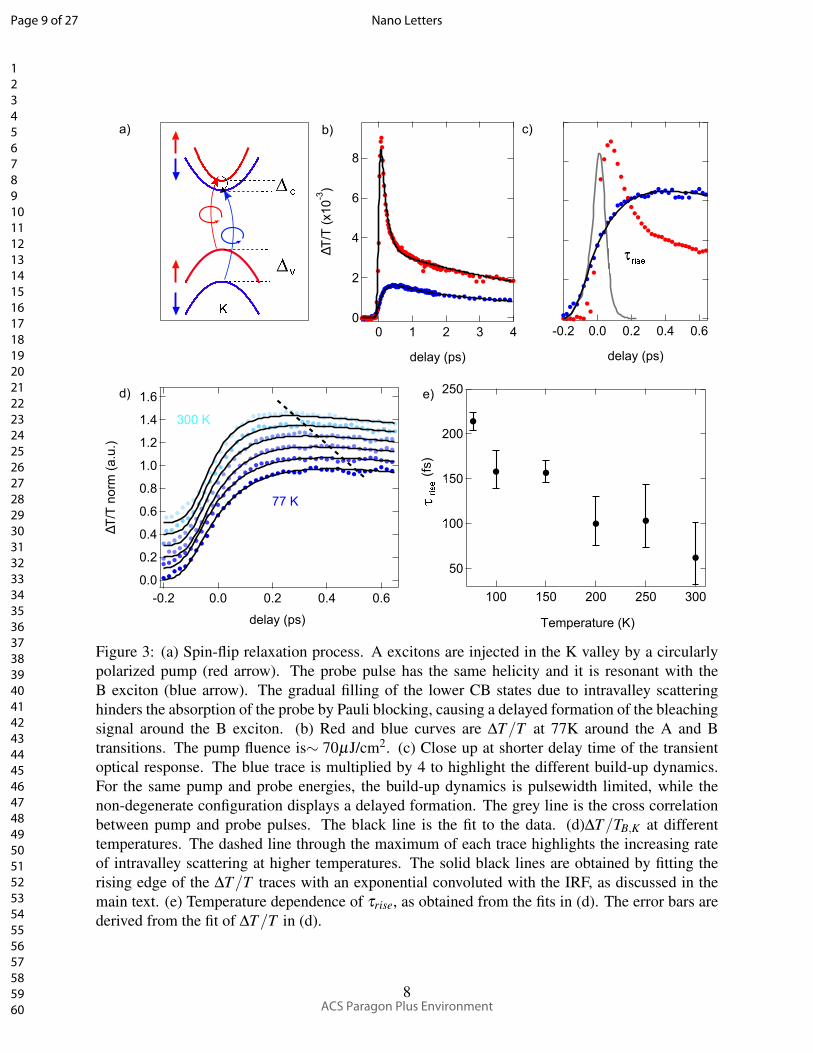
Henceforth, we will focus on the study of the valley-resolved temporal dynamics on a narrow
energy range, centered around the maximum of the A/B exciton bleaching signals. We thus per-
form two-color helicity-resolved transient absorption measurements with pump and probe beams
both generated by NOPAs, in two different configurations. The pump beam is characterized by a
central energy EA=2.09eV and a bandwidth (30meV) larger than the observed energy shift of the
maximum of the A exciton PB (i.e.∼14meV), reported in Fig.2, while the probe beam is either
degenerate or non-degenerate with the pump. In the non-degenerate configuration, the probe is
characterized by a central energy EB=2.45eV and a bandwidth of 45meV. The pump is modulated
at 1kHz (i.e. half of the laser repetition rate) by a mechanical chopper. Both beams are circu-
larly polarized by a broadband quarter wave-plate (BHalle). After interaction with the sample, the
probe beam is detected by a photodiode. The readout is then demodulated by a lock-in amplifier
(Stanford SR830) enabling the detection of ∆T/T down to∼10−4.
The spin ordering of the CB states in 1L-WS2 is such that the pump excites electrons from the
upper VB to the upper CB. The photo-generated holes are not expected to scatter into the lower
VB within the time scale of our experiment, because the energy splitting of the VB in K is over
one order of magnitude higher than the CB splitting. Therefore, it is more likely for photoexcited
electrons to lose energy and scatter from upper to lower CB states, than for holes to gain energy
and scatter from the upper to lower VB states in K, consequently blocking the absorption of the
probe beam around the B exciton transition. Ref. 55 showed that the spin-flip process for holes
7
Page 8 of 27
ACS Paragon Plus Environment
Nano Letters
123456789101112131415161718192021222324252627282930313233343536373839404142434445464748495051525354555657585960
0.60.40.20.0-0.2
delay (ps)
250
200
150
100
50
300250200150100
Temperature (K)
8
6
4
2
0∆
T/T
(x10
-3)
43210
delay (ps)
c)
d) e)
300 K
77 K
a) b)
1.6
1.4
1.2
1.0
0.8
0.6
0.4
0.2
0.0
∆T
/T n
orm
(a.u
.)
0.60.40.20.0-0.2
delay (ps)
rise
v
c
rise
(fs)
Figure 3: (a) Spin-flip relaxation process. A excitons are injected in the K valley by a circularlypolarized pump (red arrow). The probe pulse has the same helicity and it is resonant with theB exciton (blue arrow). The gradual filling of the lower CB states due to intravalley scatteringhinders the absorption of the probe by Pauli blocking, causing a delayed formation of the bleachingsignal around the B exciton. (b) Red and blue curves are ∆T/T at 77K around the A and Btransitions. The pump fluence is∼ 70µJ/cm2. (c) Close up at shorter delay time of the transientoptical response. The blue trace is multiplied by 4 to highlight the different build-up dynamics.For the same pump and probe energies, the build-up dynamics is pulsewidth limited, while thenon-degenerate configuration displays a delayed formation. The grey line is the cross correlationbetween pump and probe pulses. The black line is the fit to the data. (d)∆T/TB,K at differenttemperatures. The dashed line through the maximum of each trace highlights the increasing rateof intravalley scattering at higher temperatures. The solid black lines are obtained by fitting therising edge of the ∆T/T traces with an exponential convoluted with the IRF, as discussed in themain text. (e) Temperature dependence of τrise, as obtained from the fits in (d). The error bars arederived from the fit of ∆T/T in (d).
8
Page 9 of 27
ACS Paragon Plus Environment
Nano Letters
123456789101112131415161718192021222324252627282930313233343536373839404142434445464748495051525354555657585960
in 1L-TMDs at 77K occurs through the Elliott-Yafet mechanism on a time scale∼10ns, i.e. 4-5
orders of magnitude longer than the sub-ps time scale of our experiments. Thus, in the degenerate
configuration, the probe is sensitive to the decay of the excited electron population in the upper
CB. In the non-degenerate configuration, the probe measures the electron population in the lower
CB, which is the one related to the dark excitons. With left- (right-) circular polarized light, we
can access the K (K’) valley, because of the optical selection rules. This enables us to disentangle
the intra- and intervalley scattering processes. To study the intravalley relaxation dynamics, both
pump and probe have the same helicity.
Fig.3b plots the transient absorption signal for the degenerate (red curve, ∆T/TA,K) and non-
degenerate (blue curve, ∆T/TB,K) configuration. The positive sign of both curves corresponds
to the PB of the A and B transitions. The ∆T/TA,K trace exhibits a pulse-width limited build-
up followed by a relaxation dynamics fitted by a double exponential with decay times τ f astA =
150± 10fs and τslowA = 4.5± 0.5ps. ∆T/TB,K has a single exponential decay with τB = 5± 0.5ps
and reaches its maximum at a delayed time with respect to the pump excitation, Fig.3c. The
rise time τrise = 210± 10fs is estimated by fitting the build-up dynamics with the function 1−
exp(−t/τrise) convoluted with a Gaussian instrumental response function (IRF), obtained by sum-
frequency cross-correlation experiments between pump and probe pulses, accounting for the tem-
poral resolution∼100fs.
The instantaneous rise of ∆T/TA,K is interpreted as a phase space filling of the final state by
Pauli blocking and transient optical gap renormalization. The latter is caused by the transient
change of the Coulomb screening and has a characteristic timescale (∼tens fs56) much faster than
the temporal resolution of our setup. Therefore, the finite build-up of the photobleaching signal
around the B exciton can only arise from Pauli blocking, due to the scattering of the carriers from
the upper to the lower CB at K.
Many scattering mechanisms contribute to the depletion of the bright state on a sub-ps timescale,
since bright excitons can radiatively recombine in the same valley,35 scatter into the opposite val-
ley34,36,37,44,45 or form dark excitons with non-zero momentum.57 It is often assumed that di-
9
Page 10 of 27
ACS Paragon Plus Environment
Nano Letters
123456789101112131415161718192021222324252627282930313233343536373839404142434445464748495051525354555657585960
rect intravalley scattering, requiring a spin-flip, occurs on times> 10ps.40–42,58–60 However, our
data suggest that this process might be much faster. We find that τ f astA ∼150fs is very close to
τrise ∼ 210fs. Therefore, τrise can be associated with intravalley scattering.
To gain a deeper insight into the underlying scattering mechanism, we study the temperature
dependence of ∆T/TB,K , Fig.3d. The rise time significantly decreases at higher temperatures,
Fig.3e. This suggests that intravalley spin relaxation between upper and lower CB is phonon-
assisted. Amongst all first order phonon scattering processes, only phonons with a momentum
close to zero (around Γ), can play a role. The Γ in-plane, Raman-active, optical phonons with
symmetry Γ5 at∼285cm−1 are good candidates for mediating such a scattering process within
the same valley because their energy (∼35meV) is very close to the spin splitting in the CB.61,62
Long wavelength flexural phonons have been considered, but the associated relaxation dynamics
is orders of magnitude longer than in our measurements.40,58
Fig.4 compares the ∆T/TB,K build-up dynamics at different photoinduced carrier densities
between∼ 1012 and 1013cm−2. This shows no variation of build-up and decay dynamics. This pro-
vides important information on the origin of the spin-flip scattering. Since only electron-electron
scattering is expected to depend on the number of photoexcited carriers, we neglect this process as
the main mechanism driving the spin relaxation between upper and lower CB states. Since intraval-
ley relaxation is a transition of electrons from the upper to the lower CB, we expect the scattering
time to depend on the spin splitting ∆c which, for 1L-WS2, is estimated to be∼26meV (see inset
of the band structure in Fig.10a). This is substantiated by performing the same experiments on
1L-MoS2. Here the spin ordering of the CB state at K is reversed compared to 1L-WS2, implying
that the bright exciton has lower energy than the dark one.23
Ref. 23 reported that in 1L-MoS2 chalcogen and metal atoms contributions to the CB splitting
have opposite signs and almost cancel each other, resulting in a very small CB splitting (∼3meV23)
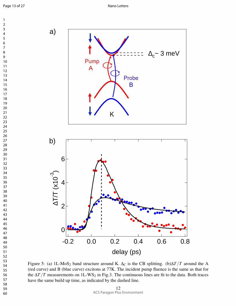
when compared to other 1L-TMDs. Fig.5 plots the transient optical response around the A (EA =
1.85eV) and B (EB = 2.05eV) excitons of 1L-MoS2 (red and blue curves respectively) after spin
polarized carriers are photoinjected in the K valley by a 100fs pump pulse in resonance with the A
10
Page 11 of 27
ACS Paragon Plus Environment
Nano Letters
123456789101112131415161718192021222324252627282930313233343536373839404142434445464748495051525354555657585960
2.0
1.5
1.0
0.5
0.0
∆T/T
(no
rm)
2.01.51.00.50.0-0.5
delay (ps)
2*1012
cm-2
3.2*1012
cm-2
4*1012
cm-2
77 K
6*1012
cm-2
8*1012
cm-2
10*1012
cm-2
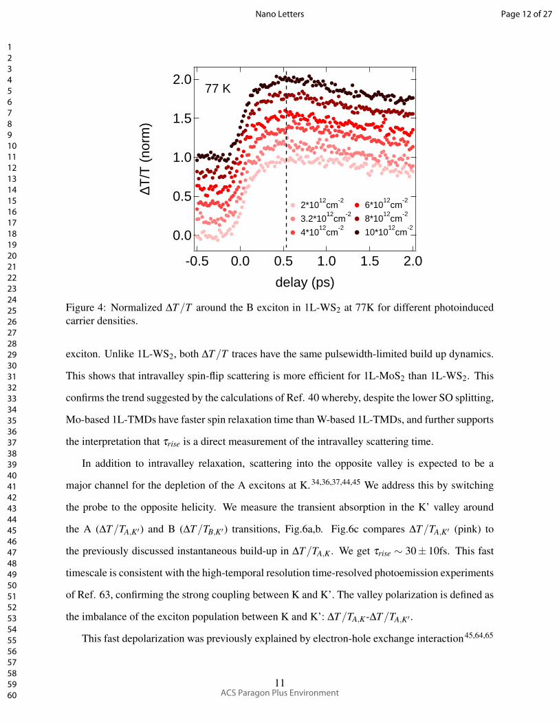
Figure 4: Normalized ∆T/T around the B exciton in 1L-WS2 at 77K for different photoinducedcarrier densities.
exciton. Unlike 1L-WS2, both ∆T/T traces have the same pulsewidth-limited build up dynamics.
This shows that intravalley spin-flip scattering is more efficient for 1L-MoS2 than 1L-WS2. This
confirms the trend suggested by the calculations of Ref. 40 whereby, despite the lower SO splitting,
Mo-based 1L-TMDs have faster spin relaxation time than W-based 1L-TMDs, and further supports
the interpretation that τrise is a direct measurement of the intravalley scattering time.
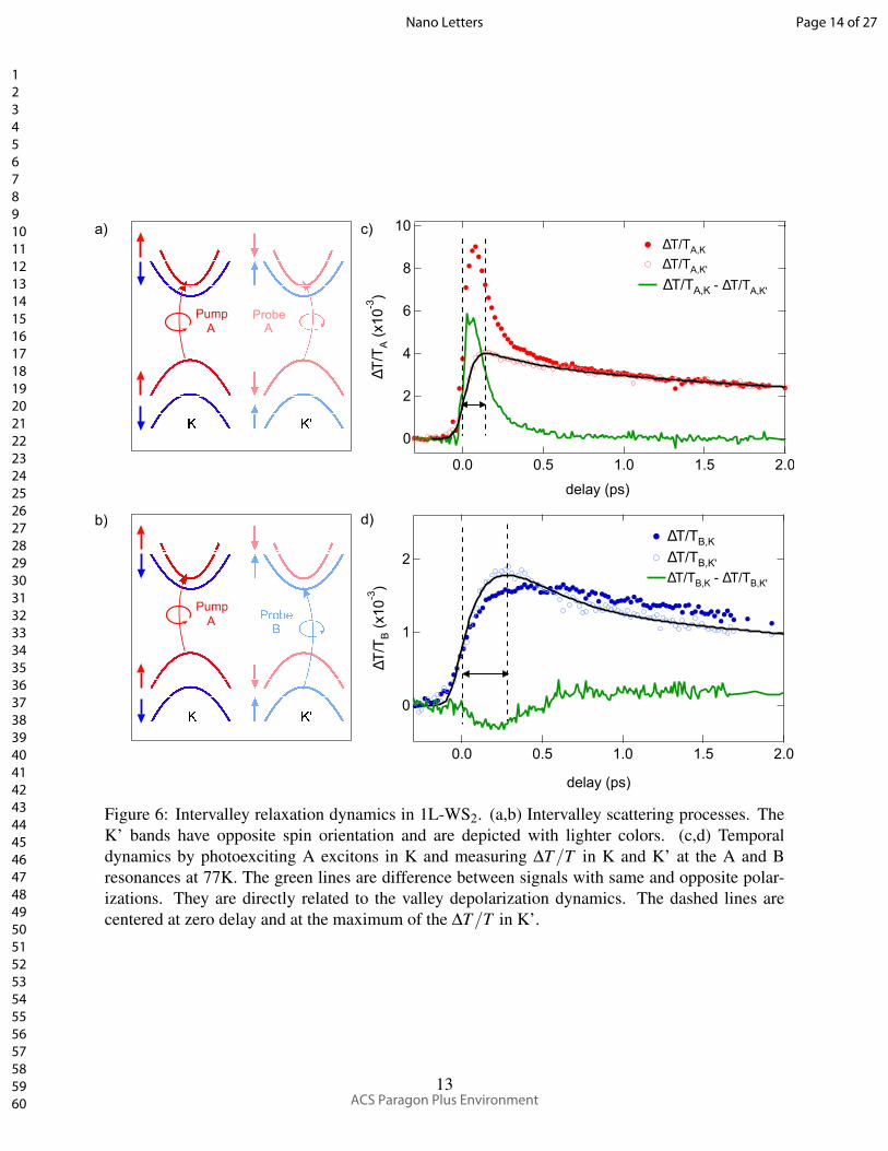
In addition to intravalley relaxation, scattering into the opposite valley is expected to be a
major channel for the depletion of the A excitons at K.34,36,37,44,45 We address this by switching
the probe to the opposite helicity. We measure the transient absorption in the K’ valley around
the A (∆T/TA,K′) and B (∆T/TB,K′) transitions, Fig.6a,b. Fig.6c compares ∆T/TA,K′ (pink) to
the previously discussed instantaneous build-up in ∆T/TA,K . We get τrise ∼ 30± 10fs. This fast
timescale is consistent with the high-temporal resolution time-resolved photoemission experiments
of Ref. 63, confirming the strong coupling between K and K’. The valley polarization is defined as
the imbalance of the exciton population between K and K’: ∆T/TA,K-∆T/TA,K′ .
This fast depolarization was previously explained by electron-hole exchange interaction45,64,65
11
Page 12 of 27
ACS Paragon Plus Environment
Nano Letters
123456789101112131415161718192021222324252627282930313233343536373839404142434445464748495051525354555657585960
6
4
2
0
∆T/T
(x1
0-3)
0.80.60.40.20.0-0.2
delay (ps)
∆c~ 3 meV
a)
b)
A
B
Figure 5: (a) 1L-MoS2 band structure around K. ∆C is the CB splitting. (b)∆T/T around the A(red curve) and B (blue curve) excitons at 77K. The incident pump fluence is the same as that forthe ∆T/T measurements on 1L-WS2 in Fig.3. The continuous lines are fit to the data. Both traceshave the same build up time, as indicated by the dashed line.
12
Page 13 of 27
ACS Paragon Plus Environment
Nano Letters
123456789101112131415161718192021222324252627282930313233343536373839404142434445464748495051525354555657585960
10
8
6
4
2
0
∆T
/TA
(x10
-3)
2.01.51.00.50.0
delay (ps)
∆T/TA,K
∆T/TA,K'
∆T/TA,K - ∆T/TA,K'
2
1
0
∆T
/TB
(x10
-3)
2.01.51.00.50.0
delay (ps)
∆T/TB,K
∆T/TB,K'
∆T/TB,K - ∆T/TB,K'
a)
b)
c)
d)
Pump
AProbe
A
Pump
A
Figure 6: Intervalley relaxation dynamics in 1L-WS2. (a,b) Intervalley scattering processes. TheK’ bands have opposite spin orientation and are depicted with lighter colors. (c,d) Temporaldynamics by photoexciting A excitons in K and measuring ∆T/T in K and K’ at the A and Bresonances at 77K. The green lines are difference between signals with same and opposite polar-izations. They are directly related to the valley depolarization dynamics. The dashed lines arecentered at zero delay and at the maximum of the ∆T/T in K’.
13
Page 14 of 27
ACS Paragon Plus Environment
Nano Letters
123456789101112131415161718192021222324252627282930313233343536373839404142434445464748495051525354555657585960
and Coulomb induced66 or phonon mediated67 intervalley scattering. Valley polarization is also
limited by intravalley scattering, which manifests on the sub-ps timescale.
Fig.6d compares the measurements of the B transition in the two valleys. The rise time in
the unpumped valley is∼ 90± 20fs. Despite the large momentum mismatch, both ∆T/TA,K′ and
∆T/TB,K′ have a faster build-up than ∆T/TB,K . The valley polarization of the B exciton (green
curve) shows a sign change, previously observed in Ref. 44, and assigned to slightly different
timescales of inter- and intravalley scattering.
To validate our conclusions, we perform time-dependent ab-initio calculations using a first-
principles implementation of non-equilibrium MBPT.68–73 We use the Quantum-Espresso suite74
to compute the equilibrium properties of 1L-WS2. The static absorption and the band structure
of 1L-WS2 are calculated using equilibrium MBPT on top of DFT, within the local density ap-
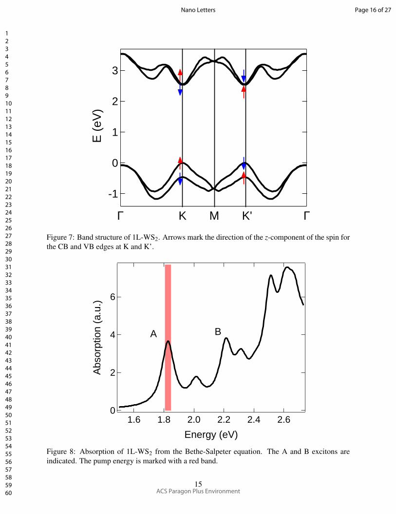
proximation (LDA), by taking into account the strong SO interaction. Fig.7 plots the calculated
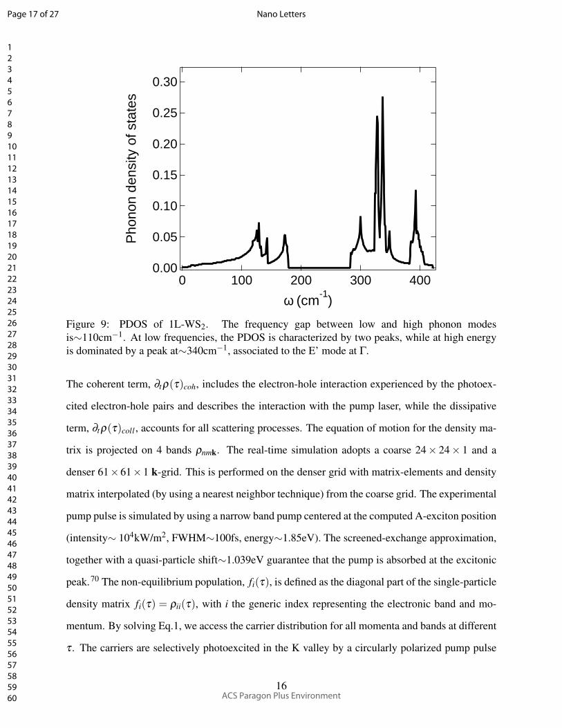
electronic bands along Γ-K-M and Γ-K′-M. Fig.8 plots the computed optical spectrum where both
GW corrections in the quasi-particle energy and SO interactions, with full spinor wave functions,
are included. We use a 24×24×1 k-grid to calculate the Bethe-Salpeter kernel. The eigenvalues
and spinorial wave-functions are calculated with 110Ry cutoff and a 15×15×1 k-point mesh. The
position of the A exciton determines the theoretical pump energy to mimic the experiments, where
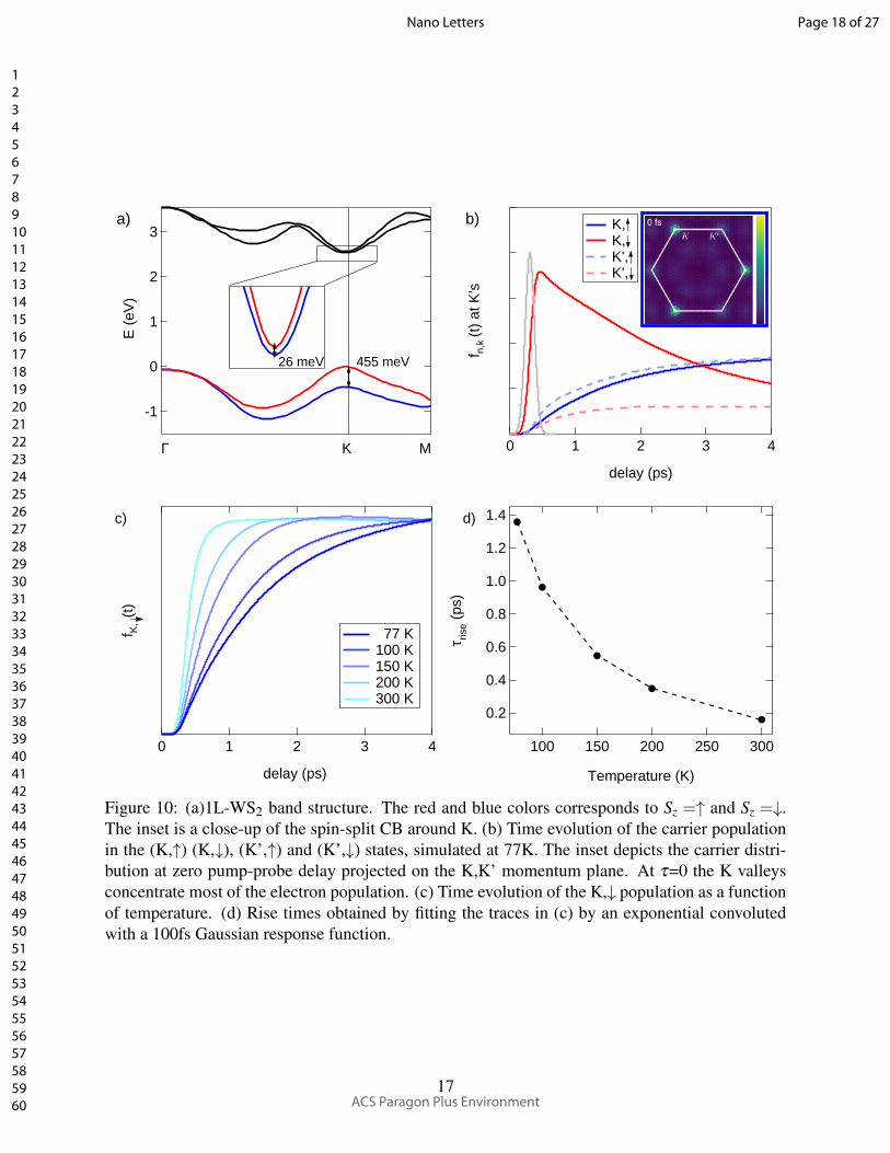
the pump is set to be resonant with A. The phonon density of states (PDOS) of 1L-WS2 is calcu-
lated using DFPT as implemented in Quantum Espresso,61 Fig.9. The calculated quasi-particle
band structure has a direct gap at K where the VB and CB SO splitting are ∆v ∼455meV and
∆c ∼26meV, as shown in Fig.10a. We consider the last two VBs and the first two CBs to describe
the carrier dynamics. Electron-phonon matrix elements are computed within DFPT. The real-time
simulation is performed with the Yambo code.75 The dynamics as a function of the pump-probe
delay τ is obtained by solving the Kadanoff-Baym equation for the one-body density matrix ρ ,
within the Generalized Kadanoff Baym ansatz:68,69
∂tρ(τ) = ∂tρ(τ)coh +∂tρ(τ)coll (1)
14
Page 15 of 27
ACS Paragon Plus Environment
Nano Letters
123456789101112131415161718192021222324252627282930313233343536373839404142434445464748495051525354555657585960
3
2
1
0
-1
E (
eV)
KΓ M K' Γ
Figure 7: Band structure of 1L-WS2. Arrows mark the direction of the z-component of the spin forthe CB and VB edges at K and K’.
6
4
2
0
Abs
orpt
ion
(a.u
.)
2.62.42.22.01.81.6
Energy (eV)
A B
Figure 8: Absorption of 1L-WS2 from the Bethe-Salpeter equation. The A and B excitons areindicated. The pump energy is marked with a red band.
15
Page 16 of 27
ACS Paragon Plus Environment
Nano Letters
123456789101112131415161718192021222324252627282930313233343536373839404142434445464748495051525354555657585960
0.30
0.25
0.20
0.15
0.10
0.05
0.00
Pho
non
dens
ity o
f sta
tes
4003002001000
ω (cm-1
)
Figure 9: PDOS of 1L-WS2. The frequency gap between low and high phonon modesis∼110cm−1. At low frequencies, the PDOS is characterized by two peaks, while at high energyis dominated by a peak at∼340cm−1, associated to the E’ mode at Γ.
The coherent term, ∂tρ(τ)coh, includes the electron-hole interaction experienced by the photoex-
cited electron-hole pairs and describes the interaction with the pump laser, while the dissipative
term, ∂tρ(τ)coll , accounts for all scattering processes. The equation of motion for the density ma-
trix is projected on 4 bands ρnmk. The real-time simulation adopts a coarse 24× 24× 1 and a
denser 61×61×1 k-grid. This is performed on the denser grid with matrix-elements and density
matrix interpolated (by using a nearest neighbor technique) from the coarse grid. The experimental
pump pulse is simulated by using a narrow band pump centered at the computed A-exciton position
(intensity∼ 104kW/m2, FWHM∼100fs, energy∼1.85eV). The screened-exchange approximation,
together with a quasi-particle shift∼1.039eV guarantee that the pump is absorbed at the excitonic
peak.70 The non-equilibrium population, fi(τ), is defined as the diagonal part of the single-particle
density matrix fi(τ) = ρii(τ), with i the generic index representing the electronic band and mo-
mentum. By solving Eq.1, we access the carrier distribution for all momenta and bands at different
τ . The carriers are selectively photoexcited in the K valley by a circularly polarized pump pulse
16
Page 17 of 27
ACS Paragon Plus Environment
Nano Letters
123456789101112131415161718192021222324252627282930313233343536373839404142434445464748495051525354555657585960
f K,
(t)
43210
delay (ps)
77 K 100 K 150 K 200 K 300 K
3
2
1
0
-1
E (
eV)
KΓ M
455 meV26 meV
f n,k
(t)
at K
's
43210
delay (ps)
K, K, K', K',
a)
c)
b)
d) 1.4
1.2
1.0
0.8
0.6
0.4
0.2
τ rise
(ps)
300250200150100
Temperature (K)
Figure 10: (a)1L-WS2 band structure. The red and blue colors corresponds to Sz =↑ and Sz =↓.The inset is a close-up of the spin-split CB around K. (b) Time evolution of the carrier populationin the (K,↑) (K,↓), (K’,↑) and (K’,↓) states, simulated at 77K. The inset depicts the carrier distri-bution at zero pump-probe delay projected on the K,K’ momentum plane. At τ=0 the K valleysconcentrate most of the electron population. (c) Time evolution of the K,↓ population as a functionof temperature. (d) Rise times obtained by fitting the traces in (c) by an exponential convolutedwith a 100fs Gaussian response function.
17
Page 18 of 27
ACS Paragon Plus Environment
Nano Letters
123456789101112131415161718192021222324252627282930313233343536373839404142434445464748495051525354555657585960
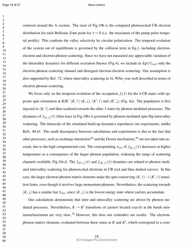
centered around the A exciton. The inset of Fig.10b is the computed photoexcited CB electron
distribution for each Brillouin Zone point for τ = 0 (i.e. the maximum of the pump pulse tempo-
ral profile). This confirms the valley selectivity by circular polarization. The temporal evolution
of the system out of equilibrium is governed by the collision term in Eq.1, including electron-
electron and electron-phonon scattering. Since we have not measured any appreciable variation of
the intravalley dynamics for different excitation fluence (Fig.4), we include in ∂tρ(τ)coll only the
electron-phonon scattering channel and disregard electron-electron scattering. Our assumption is
also supported by Ref. 72, where intervalley scattering in 1L-WSe2 was well described in terms of
electron-phonon scattering.
We focus only on the temporal evolution of the occupation fi(τ) for the 4 CB states with op-
posite spin orientation at K/K’ (K,↑) (K,↓), (K′,↑) and (K′,↓) (Fig. 6a). The population is first
injected in (K,↑) and then scattered towards the other 3 states by phonon mediated processes. The
dynamics of f(K,↓)(τ) (blue trace in Fig.10b) is governed by phonon-mediated spin-flip intravalley
scattering. The timescale of the simulated build-up dynamics reproduces our experiments, unlike
Refs. 40,41. The small discrepancy between calculations and experiments is due to the fact that
other processes, such as exchange interaction64 and the Dexter mechanism,44 are not taken into ac-
count, due to the high computational cost. The corresponding τrise of f(K,↓)(τ) decreases at higher
temperature as a consequence of the larger phonon population, widening the range of scattering
channels available, Fig.10c,d. The f(K′,↓)(τ) and f(K′,↑)(τ) dynamics are related to phonon medi-
ated intervalley scattering for photoexcited electrons in CB (red and blue dashed curves). In this
case, the larger electron-phonon matrix elements make the spin-conserving (K,↑)→ (K′,↑) transi-
tion faster, even though it involves large momentum phonons. Nevertheless, the scattering towards
(K,↓) has a similar fast τrise, since (K,↓) is the lowest energy state where carriers accumulate.
Our calculations demonstrate that inter and intravalley scattering are driven by phonon me-
diated processes. Nevertheless, K → K′ transitions of carriers located exactly at the bands min-
imum/maximum are very slow.76 However, this does not contradict our results. The electron-
phonon matrix elements, evaluated between these states at K and K′, which correspond to a com-
18
Page 19 of 27
ACS Paragon Plus Environment
Nano Letters
123456789101112131415161718192021222324252627282930313233343536373839404142434445464748495051525354555657585960
plete spin flip, are zero. Therefore the K → K′ dynamics of such localized carriers is much slower
that the dynamics observed experimentally. This apparent discrepancy is reconciled by observ-
ing that the carriers are distributed around K and K′, due to the finite laser energy bandwidth,
the broadening of the states (proportional to the density of states) caused by quasi-particle correc-
tions18 and the fast intravalley scattering that tends to equilibrate carries in the valley by creating
a Fermi-Dirac distribution with a finite temperature. Thus, the inter and intravalley dynamics in
Fig.10b is caused by the scattering of carriers around K and K′. The strength of the interaction and
the speed of the transitions are dictated by the density of carriers around the band minima/maxima.
Our simulations predict build-up times of fi(τ) slower than the measured ∆T/T . This can be
explained by phenomena not included in our calculations, like the pump-induced optical gap renor-
malization or the Dexter mechanism.44 In order to include the optical gap renormalization effect,
the temporal evolution of the non-equilibrium optical spectrum has to be simulated. In Ref. 50
we have done this by computing the non-equilibrium carrier population created by the pump pulse
and the additional Coulomb screening caused by the modification of the electronic occupations.
However, this is restricted to a single time delay.50 For an extended temporal range (i.e. the first
few ps after pump excitation) this becomes computationally extremely demanding. At present,
the Dexter mechanism has only been implemented with semi-empirical approaches, selecting ad-
hoc the participating exciton states.44 A non-equilibrium ab-initio formalism including the Dexter
mechanism has not been developed yet. Despite this, the electron-phonon interaction remains the
driving mechanism which explains the experimental temperature dependence.
In conclusion, we studied intra- and intervalley relaxation dynamics in 1L-WS2 by two-color
helicity-resolved transient absorption spectroscopy. This allowed us to separately probe and disen-
tangle these processes. Intravalley relaxation is fast (<1ps), leading to a very efficient depletion of
the bright A exciton. The temperature dependence of the intravalley scattering rate is a signature
of a phonon-mediated process, which depends on the value of the CB spin splitting. Ab-initio
simulations are in good agreement with experiments, confirming the fast timescale. The valley po-
larization in 1L-WS2 has a similarly fast relaxation time, suggesting a strong interaction between
19
Page 20 of 27
ACS Paragon Plus Environment
Nano Letters
123456789101112131415161718192021222324252627282930313233343536373839404142434445464748495051525354555657585960
the two valleys. We stress that, since intravalley spin flip and intervalley scattering processes are
effective on the same timescale, the former relaxation mechanism cannot be disregarded in ex-
plaining the fast valley depolarization of A excitons in 1L-WS2. Since the intravalley scattering
process determines the formation of the dark intravalley exciton, our results indicate that the bright
to dark intravalley exciton transition occurs on a sub-ps timescale. Our work has implications for
the emerging fields of valleytronics and optoelectronics with layered semiconductors, because it
demonstrates that, unlike previous assumptions, intravalley spin-flip scattering is an efficient decay
channel for valley polarization. Our results clarify the mechanisms leading to fast degradation of
the valley polarization in TMDs and, at the same time, shed light on the scattering processes which
limit light emission efficiency in optoelectronic and photonic devices based on 1L-TMDs, such as
light emitting diodes77 and polarized photon emitters.78
Acknowledgement
We thank Andreas Knorr, Mikhail Glazov, Alexey Chernikov and Ivan Bernal-Villamil for useful
discussions. We acknowledge funding from the National Research Fund, Luxembourg (Projects
C14/MS/773152/ FAST-2DMAT and INTER/ANR/13/20/NANOTMD), the Juan de la Cierva Pro-
gram, the EU Graphene Flagship, ERC grant Hetero2D, EPSRC grants EP/L016087/1, EP/K01711X/1,
EP/K017144/1, the Early Postdoc Mobility program of the Swiss National Science Foundation
(P2BSP2 168747), the EU project MaX Materials design at the eXascale H2020-EINFRA-2015-1,
and Nanoscience Foundries and Fine Analysis-Europe H2020-INFRAIA-2014-2015.
References
(1) Wang, Q. H.; Kalantar-Zadeh, K.; Kis, A.; Coleman, J. N.; Strano, M. S. Nat. Nano. 2012,
7, 699–712.
(2) Koppens, F. H. L.; Mueller, T.; Avouris, P.; Ferrari, A. C.; Vitiello, M. S.; Polini, M. Nat.
Nano., 2014, 9, 780–793.
20
Page 21 of 27
ACS Paragon Plus Environment
Nano Letters
123456789101112131415161718192021222324252627282930313233343536373839404142434445464748495051525354555657585960
(3) Mak, K. F.; Shan J. Nat. Photon., 2016, 10, 216–226.
(4) Ferrari, A. C.; Bonaccorso, F.; Fal’ko, V.; Novoselov, K. S.; Roche, S.; Boggild, P.; Borini,
S.; Koppens, F. H. L.; Palermo, V.; Pugno, N.; et al. Nanoscale, 2015, 7, 4598–4810.
(5) Yuan, H.; Wang, X.; Lian, B.; Zhang, H.; Fang, X.; Shen, B.; Xu, G.; Xu, Y.; Zhang, S. -C.;
Hwang, H. Y.; et al. Nat. Nano., 2014, 9, 851–857.
(6) Yao, W.; Xiao, D.; Niu, Q. Phys. Rev. B: Condens. Matter Mater. Phys., 2008, 77, 235406.
(7) Aivazian, G.; Gong, Z.; Jones, A. M.; Chu, R. -L.; Yan, J.; Mandrus, D. G.; Zhang, C.;
Cobden, D.; Yao, W.; Xu, X. Nat. Phys., 2015, 11, 148–152.
(8) Ye, Y.; Xiao, J.; Wang, H.; Ye, Z.; Zhu, H.; Zhao, M.; Wang, Y.; Zhao, J.; Yin, X.; Zhang
X. Nat. Nano., 2016, 11, 598–602.
(9) Schaibley, J. R.; Yu, H.; Clark, G.; Rivera, P.; Ross, J. S.; Seyler, K. L.; Yao, W.; Xu, X.
Nat. Rev. Mat., 2016, 1, 16055.
(10) Srivastava, A.; Sidler, M.; Allain, A. V.; Lembke, D. S.; Kis, A.; Imamoglu, A. Nat. Nano,
2015,10, 491–496.
(11) Mak, K. F.; Lee, C.; Hone, J.; Shan, J.; Heinz, T. F. Phys. Rev. Lett., 2010, 105, 136805.
(12) Chernikov, A.; Berkelbach, T. C.; Hill, H. M.; Rigosi, A.; Li, Y.; Aslan, O. B.; Reichman,
D. R.; Hybertsen, M. S.; Heinz, T. F. Phys. Rev. Lett., 2014, 113, 076802.
(13) Ugeda, M. M.; Bradley, A. J.; Shi, S.-F.; da Jornada, F. H.; Zhang, Y.; Qiu, D. Y.; Ruan, W.;
Mo, S.-K.; Hussain, Z.; Shen, Z.-X.; et al. Nat. Mater., 2014, 13, 1091–1095.
(14) Zhu, B.; Chen, X.; Cui, X. Sci. Rep., 2015, 5, 9218.
(15) Komsa, H.-P.; Krasheninnikov, A. V. Phys. Rev. B, 2012, 86, 241201.
(16) Qiu, D. Y.; da Jornada, F. H.; Louie, S. G. Phys. Rev. Lett., 2013, 111, 216805.
21
Page 22 of 27
ACS Paragon Plus Environment
Nano Letters
123456789101112131415161718192021222324252627282930313233343536373839404142434445464748495051525354555657585960
(17) Molina-Sánchez, A.; Hummer, K.; Wirtz, L. Surf. Sci. Rep., 2015, 70, 554–586.
(18) Molina-Sánchez, A.; Palummo, M.; Marini, A.; Wirtz, L. Phys. Rev. B, 2016, 93, 155435.
(19) Zhang, Y.; Chang, T.-R.; Zhou, B.; Cui, Y.-T.; Yan, H.; Liu, Z.; Schmitt, F.; Lee, J.; Moore,
R.; Chen, Y.; et al. Nat. Nano., 2014, 9, 111–115.
(20) Splendiani, A.; Sun, L.; Zhang, Y.; Li, T.; Kim, J.; Chim, C.-Y.; Galli, G.; Wang, F. Nano
Lett., 2010, 10, 1271–1275.
(21) Molina-Sánchez, A.; Sangalli, D.; Hummer, K.; Marini, A.; Wirtz, L. Phys. Rev. B, 2013,
88, 045412.
(22) Li, Y.; Chernikov, A.; Zhang, X.; Rigosi, A.; Hill, H. M.; van der Zande, A. M.; Chenet,
D. A.; Shih, E.-M.; Hone, J.; Heinz, T. F. Phys. Rev. B, 2014, 90, 205422.
(23) Kosmider, K.; González, J. W.; Fernández-Rossier, J. Phys. Rev. B, 2013, 88, 245436.
(24) Kormányos, A.; Zólyomi, V.; Drummond, N. D.; Burkard, G. Phys. Rev. X, 2014, 4, 011034.
(25) Mak, K. F.; He, K.; Shan, J.; Heinz, T. F. Nat. Nano., 2012, 7, 494–498.
(26) Cao, T.; Wang, G.; Han, W.; Ye, H.; Zhu, C.; Shi, J.; Niu, Q.; Tan, P.; Wang, E.; Liu, B.;
et al. Nat. Commun., 2012, 3, 887.
(27) Zeng, H.; Dai, J.; Yao, W.; Xiao, D.; Cui, X. Nat. Nano., 2012, 7, 490–493.
(28) Yu, H.; Cui, X.; Xu, X.; Yao, W. National Science Review, 2015, 2, 57–70.
(29) Baranowski, M.; Surrente, A.; Maude, D. K.; Ballottin, M.; Mitioglu, A. A.; Christianen,
P. C. M.; Kung, Y. C.; Dumcenco, D.; Kis, A.; Plochocka, P. 2D Mater., 2017, 4, 025016.
(30) Slobodeniuk, A. O.; Basko, D. M. 2D Mater., 2016, 3, 035009.
(31) Zhang, X.-X.; Cao, T.; Lu, Z.; Lin, Y.-C.; Zhang, F.; Wang, Y.; Li, Z.; Hone, J. C.; Robinson,
J. A.; Smirnov, D.; et al. Nat. Nano., 2017, 12, 883–888.
22
Page 23 of 27
ACS Paragon Plus Environment
Nano Letters
123456789101112131415161718192021222324252627282930313233343536373839404142434445464748495051525354555657585960
(32) Molas, M. R.; Faugeras, C.; Slobodeniuk, A. O.; Nogajewski, K.; Bartos, M.; Basko, D. M.;
Potemski, M. 2D Mater., 2017, 4, 021003.
(33) Zhang, X.-X.; You, Y.; Zhao, S. Y. F.; Heinz, T. F. Phys. Rev. Lett., 2015, 115, 257403.
(34) Dal Conte, S.; Bottegoni, F.; Pogna, E. A. A.; De Fazio, D.; Ambrogio, S.; Bargigia, I.;
D’Andrea, C.; Lombardo, A.; Bruna, M.; Ciccacci, F.; et al. Phys. Rev. B, 2015, 92, 235425.
(35) Zhu, C. R.; Zhang, K.; Glazov, M.; Urbaszek, B.; Amand, T.; Ji, Z. W.; Liu, B. L.; Marie,
X. Phys. Rev. B, 2014, 90, 161302.
(36) Mai, C.; Semenov, Y. G.; Barrette, A.; Yu, Y.; Jin, Z.; Cao, L.; Kim, K. W.; Gundogdu, K.
Phys. Rev. B, 2014, 90, 041414.
(37) Mai, C.; Barrette, A.; Yu, Y.; Semenov, Y. G.; Kim, K. W.; Cao, L.; Gundogdu, K. Nano
Lett., 2014, 14, 202–206.
(38) Plechinger, G.; Nagler, P.; Arora, A.; Schmidt, R.; Chernikov, A.; del Aguila, A. G.; Chris-
tianen, P. C. M.; Bratschitsch, R.; Schüller, C.; Korn, T. Nat. Commun., 2016, 7, 12715.
(39) Plechinger, G.; Korn, T.; Lupton, J. M. J. Phys. Chem. C, 2017, 121, 6409–6413.
(40) Song, Y.; Dery, H. Phys. Rev. Lett., 2013, 111, 026601.
(41) Ochoa, H.; Roldán, R. Phys. Rev. B, 2013, 87, 245421.
(42) Wang, L.; Wu, M. W. Phys. Rev. B, 2014, 89, 115302.
(43) Glazov, M. M.; Amand, T.; Marie, X.; Lagarde, D.; Bouet, L.; Urbaszek, B. Phys. Rev. B,
2014, 89, 201302(R).
(44) Berghäuser, G.; Bernal-Villamil, I.; Schmidt, R.; Schneider, R.; Niehues, I.; Erhart, P.;
Michaelis de Vasconcellos, S.; Bratschitsch, R.; Knorr, A.; Malic, E. Nat. Commun., 2018,
9, 971.
23
Page 24 of 27
ACS Paragon Plus Environment
Nano Letters
123456789101112131415161718192021222324252627282930313233343536373839404142434445464748495051525354555657585960
(45) Manca, M.; Glazov, M. M.; Robert, C.; Cadiz, F.; Taniguchi, T.; Watanabe, K.; Courtade,
E.; Amand, T.; Renucci, P.; Marie, X.; et al. Nat. Commun., 2017, 8, 14927.
(46) Jin, C.; Kim, J.; Wu, K.; Chen, B.; Barnard, E. S.; Suh, J.; Shi, Z.; Drapcho, S. G.; Wu, J.;
Schuck, P. J.; et al. Adv. Funct. Mater., 2016, 27, 1601741.
(47) Castellanos-Gomez, A.; Buscema, M.; Molenaar, R.; Singh, V.; Janssen, L.; van der Zant,
H. S. J.; Steele, G.A. 2D Mater., 2014, 1, 011002.
(48) Berkdemir, A.; Gutiérrez, H. R.; Botello-Méndez, A. R.; Perea-López, N.; Elías, A. L.;
Chia, C.-I.; Wang, B.; Crespi, V.H.; López-Urías, F.; Charlier, J.-C.; et al. Sci. Rep., 2013,
3, 1755.
(49) Gutiérrez, H. R.; Perea-López, N.; Elías, A. L.; Berkdemir, A.; Wang, B.; Lv, R.; López-
Urías, F.; Crespi, V. H.; Terrones, H.; Terrones, M. Nano Lett., 2013, 13, 3447–3454.
(50) Pogna, E. A. A.; Marsili, M.; De Fazio, D.; Dal Conte, S.; Manzoni, C.; Sangalli, D.; Yoon,
D.; Lombardo, A.; Ferrari, A. C.; Marini, A.; et al. ACS Nano, 2016, 10, 1182–1188.
(51) Sim, S.; Park, J.; Song, J.-G.; In, C.; Lee, Y.-S.; Kim, H.; Choi, H. Phys. Rev. B, 2013, 88,
075434.
(52) Vega-Mayoral, V.; Vella, D.; Borzda, T.; Prijatelj, M.; Tempra, I.; Pogna, E. A. A.; Dal
Conte, S.; Topolovsek, P.; Vujicic, N.; Cerullo, G.; et al. Nanoscale, 2016, 8, 5428–5434.
(53) Ruppert, C.; Chernikov, A.; Hill, H. M.; Rigosi, A. F.; Heinz, T. F. Nano Lett., 2017, 17,
644–651.
(54) Sie, E. J.; Steinhoff, A.; Gies, C.; Lui, C. H.; Ma, Q.; Rösner, M.; Schönhoff, G.; Jahnke,
F.; Wehling, T. O.; Lee, et al. Nano Lett., 2017, 17 (7), 4210–4216.
(55) Kim, J.; Jin, C.; Chen, B.; Cai, H.; Zhao, T.; Lee, P.; Kahn, S.; Watanabe, K.; Taniguchi, T.;
Tongay, S.; et al. Sci. Adv., 2017, 3, e1700518.
24
Page 25 of 27
ACS Paragon Plus Environment
Nano Letters
123456789101112131415161718192021222324252627282930313233343536373839404142434445464748495051525354555657585960
(56) Huber, R.; Tauser, F.; Brodschelm, A.; Bichler, M.; Abstreiter, G.; Leitenstorfer, A. Na-
ture,2001, 414, 286–289.
(57) Selig, M.; Berghäuser, G.; Richter, M.; Bratschitsch, R.; Knorr, A.; Malic, E. 2D Mater.,
2018, 5, 035017.
(58) Ochoa, H.; Guinea, F.; Fal’ko, V. I. Phys. Rev. B, 2013, 88, 195417.
(59) Ochoa, H.; Finocchiaro, F.; Guinea, F.; Fal’ko, V. I. Phys. Rev. B, 2014, 90, 235429.
(60) Schmidt, H.; Yudhistira, I.; Chu, L.; Castro Neto, A. H.; Ozyilmaz, B.; Adam, S.; Eda, G.
Phys. Rev. Lett., 2016, 116, 046803.
(61) Molina-Sánchez, A.; Wirtz, L. Phys. Rev. B, 2011, 84, 155413.
(62) Danovich, M.; Aleiner, I. L.; Drummond, N. D.; Fal’ko, V. I. IEEE J. Sel. Top. Quantum
Electron., 2017, 23, 168–172.
(63) Bertoni, R.; Nicholson, C. W.; Waldecker, L.; Hübener, H.; Monney, C.; De Giovannini, U.;
Puppin, M.; Hoesch, M.; Springate, E.; Chapman, R. T.; et al. Phys. Rev. Lett., 2016, 117,
277201.
(64) Yu, T.; Wu, M. W. Phys. Rev. B, 2014, 89, 205303.
(65) Yu, H.; Liu, G.-B.; Gong, P.; Xu, X.; Yao, W. Nat. Commun., 2014, 5, 3876.
(66) Schmidt, R.; Berghäuser, G.; Schneider, R.; Selig, M.; Tonndorf, P.; Malic, E.; Knorr, A.;
Michaelis de Vasconcellos, S.; Bratschitsch, R. Nano Lett., 2016, 16, 2945–2950.
(67) Carvalho, B. R.; Wang, Y.; Mignuzzi, S.; Roy, D.; Terrones, M.; Fantini, C.; Crespi, V. H.;
Malard, L. M.; Pimenta, M. A. Nat. Commun., 2017, 8, 14670.
(68) Marini, A. J. Phys.: Conf. Ser., 2013, 427, 012003.
(69) Sangalli, D.; Marini, A. J. Phys.: Conf. Ser., 2015, 609, 012006.
25
Page 26 of 27
ACS Paragon Plus Environment
Nano Letters
123456789101112131415161718192021222324252627282930313233343536373839404142434445464748495051525354555657585960
(70) Attaccalite, C.; Grüning, M.; Marini, A. Phys. Rev. B, 2011, 84, 245110.
(71) Perfetto, E.; Sangalli, D.; Marini, A.; Stefanucci, G. Phys. Rev. B, 2015, 92, 205304.
(72) Molina-Sánchez, A.; Sangalli, D.; Wirtz, L.; Marini, A. Nano Lett., 2017, 17, 4549–4555.
(73) Sangalli, D.; Perfetto, E.; Stefanucci, G.; Marini, A. Eur. Phys. J. B, 2018, 91, 171.
(74) Giannozzi, P.; Baroni, S.; Bonini, N.; Calandra, M.; Car, R.; Cavazzoni, C.; Ceresoli, D.;
Chiarotti, G.L.; Cococcioni, M.; Dabo, I.; et al. J. Phys. C, 2009, 21, 395502.
(75) Marini, A.; Hogan, C.; Grüning, M.; Varsano, D. Comput. Phys. Commun., 2009, 180,
1392–1403.
(76) Kaasbjerg, K.; Thygesen, K. S.; Jacobsen, K. W. Phys. Rev. B, 2012, 85, 115317.
(77) Palacios-Berraquero, C.; Barbone, M.; Kara, D. M.; Chen, X.; Goykhman, I.; Yoon, D.; Ott,
A. K.; Beitner, J.; Watanabe, K.; Taniguchi, T.; et al. Nat. Commun., 2016, 7, 12978.
(78) Lodahl, P.; Mahmoodian, S.; Stobbe, S.; Rauschenbeutel, A.; Schneeweiss, P.; Volz, J.;
Pichler, H.; Zoller, P. Nature, 2017, 541, 473–480.
26
Page 27 of 27
ACS Paragon Plus Environment
Nano Letters
123456789101112131415161718192021222324252627282930313233343536373839404142434445464748495051525354555657585960