Study on Three-Phase Four-Wire UPQC device for Power ... · Study on Three-Phase Four-Wire UPQC...
12
© 2014 IJEDR | Volume 2, Issue 3 | ISSN: 2321-9939 IJEDR1403058 International Journal of Engineering Development and Research ( www.ijedr.org) 3165 Study on Three-Phase Four-Wire UPQC device for Power Quality Improvement 1 Sumaya Banu, 2 Dr. Sidheswar Prasad 1 M.Tech, 2 Professor 1 Department of Electricals and Electronics , 1 The Oxford College of Engineering, Bangalore, India _______________________________________________________________________________________________________ Abstract - The unified power quality conditioner [UPQC] is one of the advanced forms of custom devices, which consists of a hybrid series filter for compensating the voltage disturbances and a shunt active power filter for eliminating current distortions. This custom power device is mainly employed to overcome the power quality [PQ] problems by improving the quality of supply voltage and its waveforms, and to minimize present harmonic contents in nonlinear load currents in power distribution systems. In this paper, the configuration of UPQC, the designs of various components of UPQC, such as series and shunt active filter VSI parameters, the controllers, etc have been designed for simulation studies against nonlinear loads using MATLAB/ Simulink environments. The simulation studies on both conventional and modified topology of UPQC are presented, which have been carried out by considering a case example of voltage sag, swell, interruption, and harmonic distortions. From the simulation results on conventional and modified UPQC topology, it can be concluded that the modified topology has less average switching frequency, less THDs in load voltages and currents from the source. It has been also observed that the modified UPQC system gives reduced dc-link voltage than the conventional UPQC topology. Index Terms—Unified Power Quality Conditioner (UPQC), Distribution Static Compensator (DSTATCOM), Dynamic Voltage Restorer (DVR), Voltage Source Inverter (VSI), Total Harmonic Distortion (THD), dc-link Voltage, average switching frequency. ________________________________________________________________________________________________________ I. INTRODUCTION In recent years, Power engineers are concerned with overall quality of the supply of electrical power. Power Quality [PQ] phenomena include all situations in which the supply voltage (voltage quality) or load current (current quality) waveforms deviate from the sinusoidal waveform at rated frequency with amplitude corresponding to peak value in all the phases for any three-phase supply system. The term Power Quality [PQ] has gained significant importance, especially in electrical power distribution system. As per the International standards, the term power quality can be defined as the physical characteristics of the electrical supply provided under normal operating condition that do not disrupt or disturb the user's processes. With the advancement of power electronics and digital control technology, the renewable energy sources are increasingly being connected to power distribution systems. On the other hand, the nonlinear loads and unbalanced loads have degraded the power quality [PQ] in the power distribution network. Voltage sags or swells and harmonics are the most frequently occuring phenomena, which are affecting most commercial and industrial customers and creating PQ problems. Custom power devices have been proposed for enhancing the quality and reliability of supply. The UPQC is one of the power electronics based custom power device, which is used to deliver power at desired standards and specifications. An ideal UPQC comprises of two core parts series connected Active Power Filter [APF] and shunt connected APF, connected in a back-to-back configuration sharing a common dc-link through an energy storage system consists of dc-capacitor. The major objective of series APF is to compensate for voltage imbalances, voltage distortion and harmonics in the line as well as to provide improved voltage regulation at utility. Whereas the function of shunt APF is to regulate current and compensate reactive and negative sequence current at the load terminals, and to reduce the dc capacitor rating by regulating the DC link voltage between the two APFs. Thus, the UPQC simultaneously acts as shunt and series active power filters. The series part of the UPQC is known as Dynamic Voltage Restorer [DVR]. It is used to maintain balanced, distortion free nominal voltage at the load. The shunt part of the UPQC is known as Distribution Static Compensator [DSTATCOM], and it is used to compensate load reactive power, harmonics and balance the load currents thereby making the source current balanced and distortion free power supply nearer to unity power factor. Conventional UPQC is constituted of two Voltage Source Converters [VSC], an injection transformer and a common DC link. The presence of injection transformer can create problems like offset due to energization of transformers, increased losses in transformer windings and high cost of the system. Thus there is a need for a better injecting device. The disturbances in voltage such as harmonics, sags, swells etc. may cause the tripping of sensitive electronic equipment which can lead to disastrous consequences in industrial plants, such as, unexpected results or a termination of the whole production line. These events are common in industrial sectors and cause high economical damage, In the above scenario, it is the source that disturbs the load or sensitive equipment. To avoid heavy economical losses, the industrial customers often install mitigation devices/ equipments to protect their own plants from such kind of disturbances. One of the most effective solutions to power quality issues in the distribution side is the installation of Unified Power Quality Conditioner. UPQC is supporting for alleviating all the voltage and current related problems.
-
Upload
nguyendiep -
Category
Documents
-
view
216 -
download
1
Transcript of Study on Three-Phase Four-Wire UPQC device for Power ... · Study on Three-Phase Four-Wire UPQC...

© 2014 IJEDR | Volume 2, Issue 3 | ISSN: 2321-9939
IJEDR1403058 International Journal of Engineering Development and Research (www.ijedr.org) 3165
Study on Three-Phase Four-Wire UPQC device for
Power Quality Improvement1Sumaya Banu,
2Dr. Sidheswar Prasad
1M.Tech,
2Professor
1Department of Electricals and Electronics ,
1The Oxford College of Engineering, Bangalore, India
_______________________________________________________________________________________________________
Abstract - The unified power quality conditioner [UPQC] is one of the advanced forms of custom devices, which consists of a
hybrid series filter for compensating the voltage disturbances and a shunt active power filter for eliminating current
distortions. This custom power device is mainly employed to overcome the power quality [PQ] problems by improving the
quality of supply voltage and its waveforms, and to minimize present harmonic contents in nonlinear load currents in
power distribution systems. In this paper, the configuration of UPQC, the designs of various components of UPQC, such as
series and shunt active filter VSI parameters, the controllers, etc have been designed for simulation studies against
nonlinear loads using MATLAB/ Simulink environments. The simulation studies on both conventional and modified
topology of UPQC are presented, which have been carried out by considering a case example of voltage sag, swell,
interruption, and harmonic distortions. From the simulation results on conventional and modified UPQC topology, it can
be concluded that the modified topology has less average switching frequency, less THDs in load voltages and currents from
the source. It has been also observed that the modified UPQC system gives reduced dc-link voltage than the conventional
UPQC topology.
Index Terms—Unified Power Quality Conditioner (UPQC), Distribution Static Compensator (DSTATCOM), Dynamic
Voltage Restorer (DVR), Voltage Source Inverter (VSI), Total Harmonic Distortion (THD), dc-link Voltage, average
switching frequency.
________________________________________________________________________________________________________
I. INTRODUCTION
In recent years, Power engineers are concerned with overall quality of the supply of electrical power. Power Quality [PQ]
phenomena include all situations in which the supply voltage (voltage quality) or load current (current quality) waveforms
deviate from the sinusoidal waveform at rated frequency with amplitude corresponding to peak value in all the phases for any
three-phase supply system. The term Power Quality [PQ] has gained significant importance, especially in electrical power
distribution system. As per the International standards, the term power quality can be defined as the physical characteristics
of the electrical supply provided under normal operating condition that do not disrupt or disturb the user's processes.
With the advancement of power electronics and digital control technology, the renewable energy sources are increasingly
being connected to power distribution systems. On the other hand, the nonlinear loads and unbalanced loads have degraded the
power quality [PQ] in the power distribution network. Voltage sags or swells and harmonics are the most frequently occuring
phenomena, which are affecting most commercial and industrial customers and creating PQ problems. Custom power devices
have been proposed for enhancing the quality and reliability of supply. The UPQC is one of the power electronics based custom
power device, which is used to deliver power at desired standards and specifications. An ideal UPQC comprises of two core parts
series connected Active Power Filter [APF] and shunt connected APF, connected in a back-to-back configuration sharing a
common dc-link through an energy storage system consists of dc-capacitor. The major objective of series APF is to compensate
for voltage imbalances, voltage distortion and harmonics in the line as well as to provide improved voltage regulation at utility.
Whereas the function of shunt APF is to regulate current and compensate reactive and negative sequence current at the load
terminals, and to reduce the dc capacitor rating by regulating the DC link voltage between the two APFs. Thus, the UPQC
simultaneously acts as shunt and series active power filters. The series part of the UPQC is known as Dynamic Voltage Restorer
[DVR]. It is used to maintain balanced, distortion free nominal voltage at the load. The shunt part of the UPQC is known as
Distribution Static Compensator [DSTATCOM], and it is used to compensate load reactive power, harmonics and balance the
load currents thereby making the source current balanced and distortion free power supply nearer to unity power factor.
Conventional UPQC is constituted of two Voltage Source Converters [VSC], an injection transformer and a common DC link.
The presence of injection transformer can create problems like offset due to energization of transformers, increased losses in
transformer windings and high cost of the system. Thus there is a need for a better injecting device.
The disturbances in voltage such as harmonics, sags, swells etc. may cause the tripping of sensitive electronic equipment
which can lead to disastrous consequences in industrial plants, such as, unexpected results or a termination of the whole
production line. These events are common in industrial sectors and cause high economical damage, In the above scenario, it is the
source that disturbs the load or sensitive equipment. To avoid heavy economical losses, the industrial customers often install
mitigation devices/ equipments to protect their own plants from such kind of disturbances. One of the most effective solutions to
power quality issues in the distribution side is the installation of Unified Power Quality Conditioner. UPQC is supporting for
alleviating all the voltage and current related problems.

© 2014 IJEDR | Volume 2, Issue 3 | ISSN: 2321-9939
IJEDR1403058 International Journal of Engineering Development and Research (www.ijedr.org) 3166
In this paper, the UPQC device for application with non-stiff source is proposed. The proposed (modified) topology enables
UPQC to have a reduced dc-link voltage without compromising its compensation capability. This proposed topology also helps to
match the dc-link voltage requirement of the shunt and series active filters of the UPQC. The topology uses a capacitor in series
with the interfacing inductor of the shunt active filter, and the system neutral is connected to the negative terminal of the dc-link
voltage to avoid the requirement of the fourth leg in the Voltage Source Inverter (VSI) of the shunt active filter. The average
switching frequency of the switches in the VSI also reduces, consequently the switching losses in the inverter reduce.
II. CONVENTIONAL AND MODIFIED VSI BASED UPQC COMPENSATED DISTRIBUTION SYSTEM
The power circuit of conventional neutral-clamped VSI topology-based UPQC is shown in Fig. 1. Even though this topology
requires two dc storage devices, each leg of the VSI can be controlled independently, and tracking is smooth with less number of
switches when compared to other VSI topologies.
Figure 1. Conventional VSI based UPQC Compensated Distribution system
In the Figure 1 Vsa, Vsb and Vsc are source voltages of phases a, b, and c respectively. Similarly, Vta, Vtb, and Vtc are terminal
voltages. The voltages Vdvra, Vdvrb, and Vdvrc are injected by the series active filter. The three-phase source currents are represented
by isa, isb, and isc, load currents are represented by ila, ilb, and ilc. The shunt active filter currents are denoted by ifa, ifb, ifc, and iln
represents the current in the neutral leg. Ls and Rs represent the feeder inductance and resistance, respectively.
The interfacing inductance and resistance of the shunt active filter are represented by Lf and Rf , respectively, and the interfacing
inductance and filter capacitor of the series active filter are represented by Lse and Cse respectively. The load constituted of both
linear and nonlinear loads. The dc-link capacitors and voltages across them are represented by Cdc1 = Cdc2 = Cdc and Vdc1 = Vdc2 =
Vdc, respectively, and the total dc-link voltage is represented by Vdbus(Vdc1 + Vdc2 =2Vdc). In this conventional topology, the
voltage across each common dc-link capacitor is chosen as 1.6 times the peak value of the source voltages.
The modified VSI based UPQC compensated distribution system is as shown in Fig. 2. In this topology, the system neutral has
been connected to the negative terminal of the dc bus along with the capacitor Cf in series with the interfacing inductance of the
shunt active filter. The passive capacitor Cf has the capability to supply a part of the reactive power required by the load, and the
active filter will compensate the balance reactive power and the harmonics present in the load. The addition of capacitor in series
with the interfacing inductor of the shunt active filter will significantly reduce the dc-link voltage requirement and consequently
reduces the average switching frequency of the switches. The reduction in the dc-link voltage requirement of the shunt active
filter enables us to the match the dc-link voltage requirement with the series active filter. This topology avoids the over rating of
the series active filter of the UPQC compensation system. The design of the series capacitor Cf and the other VSI parameters have
significant effect on the performance of the compensator. This topology uses a single dc capacitor unlike the neutral-clamped
topology and consequently avoids the need of balancing the dc-link voltages.

© 2014 IJEDR | Volume 2, Issue 3 | ISSN: 2321-9939
IJEDR1403058 International Journal of Engineering Development and Research (www.ijedr.org) 3167
Figure 2. Modified VSI based UPQC compensated distribution system
III. DESIGN OF VSI PARAMETERS
The parameters of the VSI need to be designed carefully for better tracking performance. The important
parameters that need to be taken into consideration while designing conventional VSI are Vdc, Cdc, Lf , Lse, Cse, and switching
frequency(fsw). The design details of the VSI parameters for the shunt and series active filter are given in. Based on the following
equations, the parameters of the VSIs are chosen for study.
Design of shunt active filter VSI parameters
Consider the active filter is connected to an X kVA system and deals with 0.5X kVA and 2X kVA handling capability under
transient conditions for n cycles. During transient, with an increase in system kVA load, the voltage across each dc link capacitor
(Vdc) decreases and vice versa. Allowing a maximum of 25% variation in Vdc during transient, the differential energy (ΔEc)
across Cdc is given by
ΔEc = Cdc[(1.125Vdc)2 − (0.875Vdc)
2]/2. (1)
The change in system energy (ΔEs) for a load change from 2X kVA to 0.5X kVA is
ΔEs =(2X − X/2)nT. (2)
Equating (1) and (2), the dc-link capacitor value is given by
Cdc =[ 2(2X − X/2)nT]/[(1.125Vdc)2 − (0.875Vdc)
2] (3)
where, Vm is the peak value of the source voltage, X is the kVA rating of the system, n is number of cycles, and T time period
of each cycle. An empirical study has been carried out for various values of interfacing inductance values with the variation of the
dc-link voltage in [31], with Vdc = mVm, and it is found that m =1.6 gives fairly good switching performance of the VSI. The
approximate relationship between m and minimum (fswmin), maximum switching frequency (fswmax) is obtained by analysis of
the VSI in , and this is given below. For switching frequency variation approximately from 6 kHz to10 kHz, the value of m is
1.58, which is taken as 1.6 in the study
m = 1/√(1 − fswmin/fswmax) (4)
Based on this, the shunt interfacing inductance has been derived taking into consideration of the maximum switching
frequency and is given below
Lf = mVm/4h1fswmax (5)
where
h1 =√(k1/k2)(2m2 – 1)/4m
2) fswmax (6)
where, h1 is the hysteresis band limit, k1 and k2 are proportionality constants.

© 2014 IJEDR | Volume 2, Issue 3 | ISSN: 2321-9939
IJEDR1403058 International Journal of Engineering Development and Research (www.ijedr.org) 3168
Design of Series Active Filter VSI Parameters
In order to make the series active filter system a first-order system, a resistor is added in series with the filter capacitor,
referred as switching band resistor (Rsw) . The rms value of the capacitor current can be expressed as Ise =√(I2inv − I
2l). Iinv is the
series inverter current rating and Il is the load current. The capacitor branch current is divided into two components, a
fundamental current Ise1, corresponding to the fundamental reference voltage (Vref1) and a switching frequency current Isw,
corresponding to the band voltage (Vsw).
The DVR voltage and the current of the capacitor are given by
Vdvr =√(V2ref1 + V
2sw)
Ise =√(I2
se1 + I2sw)
Vsw =IswRsw = h2/√3
Vref1 =Ise1Xse1 = Ise1/2πf1Cse (7)
where h2 is the hysteresis band voltage.The resistance (Rsw) and the capacitance (Cse) values are expressed in terms of band
voltage and rated reference voltage (Vref1),respectively, and are given by
Rsw = h2/Isw√3
Cse = Ise1/Vref12πf1 (8)
The interfacing inductor Lse has been designed based on the switching frequency of the series active filter and is given by
Lse = (Vbus)Rsw/4fswmaxh2 (9)
where Vbus is the total dc-link voltage across both the dc-link capacitors. A design example eisillustrated for a rated voltage of
230V line to neutral and the dc-link voltage reference (Vdcref ) of the conventional VSI topology has been taken as 1.6 Vm for
each capacitor. The hysteresis band (h1) is taken as 0.5 A. From (5), the interfacing inductance (Lf ) is computed to be 26 mH.
The base kVA rating of the system is taken as 5kVA.Using(3), Cdc is computed and found to be 2200 µF. The rated series VSI
voltage is chosen as 50% of the rated voltage, i.e., the maximum injection capacity of the series active filter is 115 V. The
hysteresis band (h2) for series active filter is taken as 3% of the rated voltage, i.e., 6.9 V. The maximum switching frequency of
the IGBT-based inverter is taken as 10 kHz. The series active filter current rating is choosen as 8 A and the rated load current as 7
A. interfacing inductance Lse are calculated to be 80 µF, 1.5 Ω,and5mH,respectively.The system parameters are given in Table I
for the conventional VSI topology.
Design of Cf for the Proposed VSI Topology
The design of the Cf depends upon the value to which the dc-link voltage is reduced. In general, loads with only nonlinear
components of currents are very rare, and most of the electrical loads are combination of the linear inductive and nonlinear loads.
Under these conditions, the proposed topology will work efficiently. The design of the value of Cf is carried out at the maximum
load current, i.e., with the minimum load impedance to ensure that the designed Cf will perform satisfactorily at all other loading
conditions. If Smax is the maximum kVA rating of a system and Vbase is the base voltage of the system, then the minimum
impedance in the system is given as
Zmin = V 2base/Smax= |Rl + jXl| (say). (10)
In order to achieve the unity power factor, the shunt active filter current needs to supply the required reactive component of
the load current, i.e., the fundamental imaginary part of the filter current should be equal to the imaginary part of the load current.
The filter current and load current in a particular phase are given below
Ifilter = Vinv1 − Vl1/(Rf + j(Xlf − Xcf )) (11)
Iload = Vl1Rl + jXl (12)
where, Xlf =2πfLf , Xl =2πfLl, Xcf =1/2πfCf ,and f is the supply frequency of fundamental voltage. Neglecting the interfacing
resistance and equating the imaginary parts of the the above equations gives (13)
Vl1Xl/(R2l+ X2l)=(Vinv1− Vl1/((Xlf − Xcf )2) (Xlf − Xcf ) (13)
where, Vinv1 and Vl1 are the line to neutral rms voltage of the inverter and the PCC voltage at the fundamental frequency,
respectively. The fundamental component of inverter voltage in terms of dc-link voltage is as given below
Vinv1 = 0.612Vdc/2√3 (14)
In general, if the filter current (If ) flows from the inverter terminal to the PCC, the voltage at the inverter terminal should be at a
higher potential. Due to this reason, in conventional VSI topologies, the dc-link voltage is maintained higher than the voltage at
© 2014 IJEDR | Volume 2, Issue 3 | ISSN: 2321-9939
IJEDR1403058 International Journal of Engineering Development and Research (www.ijedr.org) 3169
the PCC. Equation (15) give the KVL along the filter branch for conventional topology and the proposed modified topology,
respectively
uVdc − vl =Lfdif/dt+ Rf if (15)
Where, u attains values of 1 or −1 depending on the switching of the inverter. In (16), the fundamental voltage across the
capacitor (vcf1)adds to the inverter terminal voltage (uVdc) when the load is inductive in nature. This is because, when the load is
inductive in nature, the fundamental of the filter current leads the voltage at the PCC by 90 for reactive power compensation, and
thus the fundamental voltage across the capacitor again lags the fundamental filter current by 90 Therefore, the fundamental
voltage across the capacitor will be in phase opposition to the voltage at the PCC. Thus, the fundamental voltage across the
capacitor adds to the inverter terminal voltage. This allows us to rate the dc-link voltage at lower value than conventional design.
The designer has a choice to choose the value of dc-link voltage to be reduced, such that the LC filter in the active filter leg of
each phase offers minimum impedance to the fundamental frequency and higher impedance for switching frequency components.
In the modified topology along with the series capacitor in the shunt active filter, the system neutral is connected to the negative
terminal of the dc bus capacitor. This will introduce a positive dc voltage component in the inverter output voltage.
This is because, when the top switch is ―ON,‖ +Vdbus appears at the inverter output, and 0 V appears when the bottom switch
is ―ON.‖ Thus, the inverter output voltage will have dc voltage component along with the ac voltage. The dc voltage is blocked by
the series capacitor, and thus the voltage across the series capacitor will be having two components, one is the ac component,
which will be in phase opposition to the PCC voltage, and the other is the dc component. Whereas, in case of the conventional
topology, the inverter output voltage varies between +Vdc when top switch is ―ON‖ and −Vdc when the bottom switch ―ON.‖
Similarly, when a four-leg topology is used for shunt active filter with a single dc capacitor, the inverter output voltage varies
between +Vdbus and −Vdbus. Therefore these topologies does not contain any dc component in the inverter output voltage. The
modified topology contains only one dc capacitor as the neutral is directly connected to the negative terminal of the dc bus, thus it
avoids the need of balancing of capacitor voltages which is a major disadvantage of the neutral-clamped topology. Since the
neutral wire is directly connected to the negative terminal of the dc bus, the necessity of fourth leg in the inverter is avoided.
IV. GENERATION OF REFERENCE COMPENSATOR CURRENTS UNDER UNBALANCED AND DISTORTED
VOLTAGES
In this work, the load currents are unbalanced and distorted, these currents flow through the feeder impedance and make the
voltage at terminal unbalanced and distorted. The series active filter makes the voltages at PCC balanced and sinusoidal.
However, the voltages still contain switching frequency components and they contain some distortions. If these terminal voltages
are used for generating the shunt filter current references, the shunt algorithm results in erroneous compensation. To remove this
limitation of the algorithm, fundamental positive sequence voltages v+la1(t), v+ lb1(t),and v+ lc1(t) of the PCC voltages are
extracted and are used in control algorithm for shunt active filter. The expressions for reference compensator currents are given in
(17). In this equation, Plavg is the average load power, Ploss denotes the switching losses and ohmic losses in actual compensator,
and it is generated using a capacitor voltage PI controller. The term is obtained using a moving average filter of one cycle window
of time T in seconds. The term ϕ is the desired phase angle between the source voltage and current.
ifa
∗ =ila− isa*=ila−((vla1
+ +γ(vlb1
+−vlc1
+))(Plavg+Ploss))/∆1
+
ifb* =ilb−isb
*=ilb−((vlb1
+ +γ(vlc1
+−vla1
+))(Plavg+Ploss))/∆1
+
ifc*
=ilc−isc* =ilc−((vlc1
+ +γ(vla1
+−vlb1
+))(Plavg+Ploss))/∆1
+ (17)
where,
∆ =tan Φ/√3. The above algorithm gives balanced source currents after compensation irrespective of unbalanced and distorted supply. The
reference voltages for series active filter are given as
vdvri* =vli
* − vti
i =a, b, c (18)
where vli * represents the desired load voltages in three phases, and vdvri
* represents the reference series active filter voltage.
TABLE 1 SYSTEM PARAMETERS
System Quantities Values
System voltages 230v (line to neutral), 50 Hz
Feeder impedance Zs=1+j3.141Ω
Linear Load Zla=4+j47.5Ω,Zlb=81+j39.6Ω, Zlc=31.5+j70.9Ω
Non-linear Load three-phase full bridge rectifier load feeding R-L load of 150ohm-300mH
Shunt VSI parameters Cdc=2200µF,
Lf=26mH,Rf=1Ω
Vdbus=2*Vdc=1040v(conventional), Vdbus=560v(proposed)
Series VSI parameters Cse=80µF, Lse=5mH, Rsw=1.5Ω
Series interfacing transformer 1:1, 100V and 700 VA

© 2014 IJEDR | Volume 2, Issue 3 | ISSN: 2321-9939
IJEDR1403058 International Journal of Engineering Development and Research (www.ijedr.org) 3170
Controller Design
Once the reference quantities and the actual quantities are obtained from the measurements, the switching commands for the
VSI switches are generated using hysteresis band current control method. Hysteresis current controller scheme is based on a
feedback loop, generally with two-level comparators. The switching commands are issued whenever the error limit exceeds a
specified tolerance band ―±h.‖ Unlike the predictive controllers, the hysteresis controller has the advantage of peak current
limiting capacity apart from other merits such as extremely good dynamic performance, simplicity in implementation and
independence from load parameter variations. The disadvantage with this hysteresis method is that the converter switching
frequency is highly dependent on the ac voltage and varies with it.
Figure 3 Control block diagram for UPQC
The switching control law for shunt active filter is given as follows.
If ifa ≥ ifa *+ h1,then bottom switch is turned ON Where as top switch is turned OFF (Sa =0,Sa =1).
If ifa ≤ ifa* − h1,then top switch is turned ON where as bottom switch is turned OFF (Sa =1,Sa =0).
Similarly the switching commands for series active filter is given as follows.
If Vdvra ≥ Vdvra* + h2,then bottom switch is turned ON whereas top switch is turned OFF (Saa =0,Saa =1).
If Vdvra ≤ Vdvra* − h2,then top switch is turned ON whereas bottom switch is turned OFF (Saa =1,Saa =0)
Here only six switching commands are to be generated. These six signals along with the complementary signals will control
all the 12 switches of the two inverters.
A controller is required to control the working of UPQC whenever any fault there for this purpose PI controller is used. For
DVR control load voltage is sensed and passed through a sequence analyzer. The magnitude of the actual voltage is compared
with reference voltage width modulation (PWM) control system is applied for inverter switching so as to generate a three phase
sinusoidal voltage at the load terminals. Chopping frequency is in the range of a few KHz. the inverter is controlled with PI
controller in order to maintain voltage at the load terminals.For STATCOM control load current is sensed and passed through a
sequence analyzer. The magnitude of the actual current is compared with reference current width modulation (PWM) control
system is applied for inverter switching so as to generate a three phase sinusoidal current at the load terminals. Chopping
frequency is in the range of a few kHz, the inverter is controlled with PI controller in order to maintain current at the load
terminals.
V. SIMULATION RESULTS
Simulation results without compensation
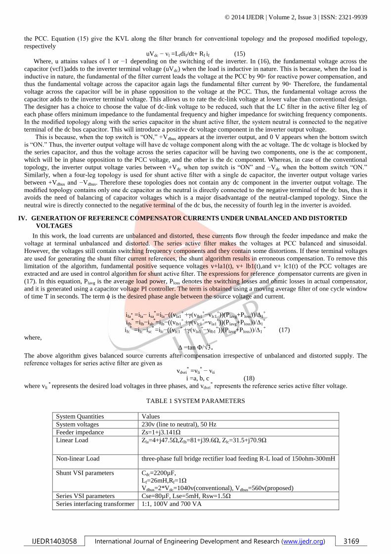
The simulation model and the output waveform for a three-phase four-wire distribution system without UPQC is shown below
in Fig. 4, which is supplying power to three-phase load through BUS 1. Vabc_s and Iabc1 state about the supply voltage and load
current at load BUS 1, which is shown in Fig. 5
Figure 4 Simulation model without compensation
Discrete,Ts = 5e-006 s.
powergui
N
R
Y
B
Subsystem1
Scope2
R
Y
B
N
LOAD
Iabc1
From7
Vabc_s
From4A
B
C
a
b
c
BUS 1
© 2014 IJEDR | Volume 2, Issue 3 | ISSN: 2321-9939
IJEDR1403058 International Journal of Engineering Development and Research (www.ijedr.org) 3171
x-time; y-voltage
Figure 5 Load current and terminal voltage before compensation
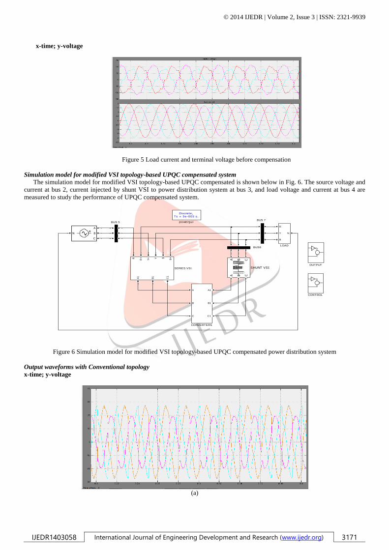
Simulation model for modified VSI topology-based UPQC compensated system
The simulation model for modified VSI topology-based UPQC compensated is shown below in Fig. 6. The source voltage and
current at bus 2, current injected by shunt VSI to power distribution system at bus 3, and load voltage and current at bus 4 are
measured to study the performance of UPQC compensated system.
Figure 6 Simulation model for modified VSI topology-based UPQC compensated power distribution system
Output waveforms with Conventional topology
x-time; y-voltage
(a)
BUS 5
BUS6
BUS 7
Discrete,Ts = 5e-005 s.
powergui
A
B
C
a
b
c
A B Ca b c
A
B
C
a
b
c
N
A
B
C
A B C
A B C
SHUNT VSI
R
R+
Y+ Y B
B+
A1
B1
C1
SERIES VSI
OUTPUT
R
Y
B
N
LOAD
A
B
C
A1
B1
C1
CONVERTERS
CONTROL

© 2014 IJEDR | Volume 2, Issue 3 | ISSN: 2321-9939
IJEDR1403058 International Journal of Engineering Development and Research (www.ijedr.org) 3172
(b)
(c)
Figure 7 (a) Source currents of conventional topology, (b) Shunt Active Filter Currents, (c) Simulation results for
compensation of voltage sag
(d)
(e)
Figure 8 (d) Simulation results for compensation of voltage swell, (e) Simulation results for compensation of interruption

© 2014 IJEDR | Volume 2, Issue 3 | ISSN: 2321-9939
IJEDR1403058 International Journal of Engineering Development and Research (www.ijedr.org) 3173
Output waveforms with modified topology
x-time; y-voltage
(f)
(g)
Figure 9 (f) Source currents (g) shunt active filter currents
(h)
(i)

© 2014 IJEDR | Volume 2, Issue 3 | ISSN: 2321-9939
IJEDR1403058 International Journal of Engineering Development and Research (www.ijedr.org) 3174
(j)
Figure 10 (h) Simulation results for compensation of voltage sag, (i) Simulation results for compensation of voltage
swell, (j) Simulation results for compensation of interruption
Harmonic analysis without compensation
For the power distribution system without and with UPQC compensation the FFT analysis is carried out and Total Harmonic
Distortion (THD) is found to be 12.38% and 7.63% and is shown below in Fig. 11.
(k)

© 2014 IJEDR | Volume 2, Issue 3 | ISSN: 2321-9939
IJEDR1403058 International Journal of Engineering Development and Research (www.ijedr.org) 3175
(l)
Figure 11 (k) Harmonic analysis without compensation, (l) Harmonic analysis with compensation
VI. ACKNOWLEDGMENT
I have a great pleasure in expressing my deep sense of gratitude to Dr. Sidheshwar Prasad, Professor, Dept. of Electrical and
Electronics Engineering, The Oxford college of Engineering, Bangalore for his willing consent, guidance and appreciation
throughout my work. I am deeply grateful to my Parents who have been supportive with their tolerance and genuine inspiration,
in equal parts.
REFERENCES
[1] M. Bollen, Understanding Power Quality Problems: Voltage Sags and Interruptions. New York: IEEE Press, 1999.
[2] S. V. R. Kumar and S. S. Nagaraju, ―Simulation of DSTATCOM and DVR in power systems,‖ ARPN J. Eng. Appl. Sci., vol.
2, no. 3, pp. 7–13,Jun. 2007.
[3] B. T. Ooi, J. C. Salmon, J. W. Dixon, and A. B. Kulkarni, ―A three-phase controlled-current PWM converter with leading
power factor,‖IEEE Trans. Ind. Appl., vol. IA-23, no. 1, pp. 78–84, Jan. 1987.
[4] Y. Ye, M. Kazerani, and V. Quintana, ―Modeling, control and implementation of three-phase PWM converters,‖ IEEE Trans.
Power Electron.,vol. 18, no. 3, pp. 857–864, May 2003.
[5] R. Gupta, A. Ghosh, and A. Joshi, ―Multiband hysteresis modulation and switching characterization for sliding-mode-
controlled cascaded multi-level inverter,‖ IEEE Trans. Ind. Electron., vol. 57, no. 7, pp. 2344–2353,Jul. 2010.
[6] S. Srikanthan and M. K. Mishra, ―DC capacitor voltage equalization in neutral clamped inverters for DSTATCOM
application,‖ IEEE Trans. Ind.Electron., vol. 57, no. 8, pp. 2768–2775, Aug. 2010.
[7] R. Gupta, A. Ghosh, and A. Joshi, ―Switching characterization of cascaded multilevel-inverter-controlled systems,‖ IEEE
Trans. Ind. Electron.,vol. 55, no. 3, pp. 1047–1058, Mar. 2008.
[8] B. Singh and J. Solanki, ―Load compensation for diesel generator-based isolated generation system employing DSTATCOM,‖
IEEE Trans. Ind.Electron., vol. 47, no. 1, pp. 238–244, Jan./Feb. 2011.
[9] R. Gupta, A. Ghosh, and A. Joshi, ―Characteristic analysis for multisampled digital implementation of fixed-switching-
frequency closed-loop modulation of voltage-source inverter,‖ IEEE Trans. Ind. Electron.,vol. 56, no. 7, pp. 2382–2392, Jul.
2009.
[10] B. Singh and J. Solanki, ―A comparison of control algorithms for DSTATCOM,‖ IEEE Trans. Ind. Electron., vol. 56, no. 7,
pp. 2738–2745,Jul. 2009.
[11] S. Rahmani, N. Mendalek, and K. Al-Haddad, ―Experimental design of a nonlinear control technique for three-phase shunt
active power filter,‖ IEEE Trans. Ind. Electron.,vol.57,no.10,pp.3364–3375,Oct.2010.
[12] V. Corasaniti, M. Barbieri, P. Arnera, and M. Valla, ―Hybrid active filter for reactive and harmonics compensation in a
distribution network,‖ IEEE Trans. Ind. Electron.,vol.56,no.3,pp.670–677,Mar.2009.
[13] M. Milane Montero, E. Romero-Cadaval, and F. Barrero-Gonzalez, ―Hybrid multi converter conditioner topology for high-
power applications,‖ IEEE Trans. Ind. Electron.,vol.58,no.6,pp.2283–2292,Jun. 2011.
[14] J. Nielsen,M. Newman, H. Nielsen, and F. Blaabjerg, ―Control and testing of a dynamic voltage restorer (DVR) at medium
voltage level,‖ IEEE Trans. Power Electron.,vol.19,no.3,pp.806–813,May2004.
[15] Y. W. Li, P. C. Loh, F. Blaabjerg, and D. Vilathgamuwa, ―Investigation and improvement of transient response of DVR at
medium voltage level,‖ IEEE Trans. Ind. Appl.,vol.43,no.5,pp.1309–1319,Sep./Oct.2007.

© 2014 IJEDR | Volume 2, Issue 3 | ISSN: 2321-9939
IJEDR1403058 International Journal of Engineering Development and Research (www.ijedr.org) 3176
[16] Y. W. Li, D. Mahinda Vilathgamuwa, F. Blaabjerg, and P. C. Loh, ―A robust control scheme for medium-voltage-level DVR
implementation,‖ IEEE Trans. Ind. Electron.,vol.54,no.4,pp.2249–2261,Aug.2007.
[17] J. Barros and J. Silva, ―Multilevel optimal predictive dynamic voltage restorer,‖ IEEE Trans. Ind.
Electron.,vol.57,no.8,pp.2747–2760, Aug. 2010.
[18] D. Vilathgamuwa, H. Wijekoon, and S. Choi, ―A novel technique to compensate voltage sags in multiline distribution
system—The interline dynamic voltage restorer,‖ IEEE Trans. Ind. Electron.,vol.53,no.5, pp. 1603–1611, Oct. 2006.
[19] M. Kesler and E. Ozdemir, ―Synchronous-reference-frame-based control mmethod for UPQC under unbalanced and distorted
load conditions,‖ IEEE Trans. Ind. Electron.,vol.58,no.9,pp.3967–3975,Sep.2011.
[20] FACTS controllers in Power Transmission and Distribution,K. R. Padiyar
[21] Understanding FACTS,Narain G. Hingorani Laszlo Gyugyi