
STUDY OF NANOSCALE MATERIALS USING POSITRON …
250
STUDY OF NANOSCALE MATERIALS USING POSITRON ANNIHILATION SPECTROSCOPY By PRIYA MAHESHWARI CHEM01200904007 Bhabha Atomic Research Centre, Mumbai A thesis submitted to the Board of Studies in Chemical Sciences In partial fulfillment of requirements For the Degree of DOCTOR OF PHILOSOPHY of HOMI BHABHA NATIONAL INSTITUTE AUGUST, 2013
Transcript of STUDY OF NANOSCALE MATERIALS USING POSITRON …

STUDY OF NANOSCALE MATERIALS USING POSITRON ANNIHILATION
SPECTROSCOPY
By
PRIYA MAHESHWARI CHEM01200904007
Bhabha Atomic Research Centre, Mumbai
A thesis submitted to the
Board of Studies in Chemical Sciences
In partial fulfillment of requirements
For the Degree of
DOCTOR OF PHILOSOPHY
of
HOMI BHABHA NATIONAL INSTITUTE
AAUUGGUUSSTT,, 22001133

HOMI BHABHA NATIONAL INSTITUTE
Recommendations of the Viva Voce Board
As members of the Viva Voce Board, we certify that we have read the dissertation
prepared by Priya Maheshwari entitled “Study of Nanoscale materials Using
Positron Annihilation Spectroscopy” and recommend that it may be accepted as
fulfilling the dissertation requirement for the Degree of Doctor of Philosophy.
Date:
Chairman: Prof. A. Goswami
Date:
Guide: Prof. P. K. Pujari
Date:
Member 1: Prof. G. Amarendra
Date:
Member 2: Prof. B. S. Tomar
Date:
Member 3: Prof. S. Kapoor
Final approval and acceptance of this dissertation is contingent upon the candidate’s
submission of the final copies of the dissertation to HBNI.
I hereby certify that I have read this dissertation prepared under my direction and
recommend that it may be accepted as fulfilling the dissertation requirement.
Date:
Place:

STATEMENT BY AUTHOR
This dissertation has been submitted in partial fulfillment of requirements for an advanced
degree at Homi Bhabha National Institute (HBNI) and is deposited in the Library to be
made available to borrowers under rules of the HBNI.
Brief quotations from this dissertation are allowable without special permission, provided
that accurate acknowledgement of source is made. Requests for permission for extended
quotation from or reproduction of this manuscript in whole or in part may be granted by
the Competent Authority of HBNI when in his or her judgment the proposed use of the
material is in the interests of scholarship. In all other instances, however, permission must
be obtained from the author.
Priya Maheshwari

DECLARATION
I, hereby declare that the investigation presented in the thesis has been carried out by me. The
work is original and has not been submitted earlier as a whole or in part for a degree /diploma
at this or any other Institution / University.
Priya Maheshwari

Dedicated to …..
My Grandparents &
Parents

List of Publications
REFFEREED JOURNALS 1. Study of iron phthalocyanine organic semiconductor thin films using slow positron
beam
P. Maheshwari, D. Dutta, S. Samanta, A. Singh, D. K. Aswal, A. V. R. Reddy and P.
K. Pujari
Phys. Stat. solidi c 6,11, (2009) 2589-2591.
2. Microstructure study of supported liquid membranes using slow positron beam
P. K. Pujari, P. Maheshwari, S. K. Sharma, D. Dutta, K. Sudarshan and A. V. R.
Reddy
Phys. Stat. solidi c 6,11, (2009)2417-2419.
3. Effect of interfacial hydrogen bonding on the freezing/melting behavior of nano-
confined liquids
P. Maheshwari, D. Dutta, S. K. Sharma, K. Sudarshan, P. K. Pujari, M. Majumdar,
B. Pahari, B. Bandyopadhyay, K. Ghosharay and A. Ghosharay
J. Phys. Chem. C,114 (2010) 4966.
4. Study of interfaces in organic semiconductor heterojunctions
P. Maheshwari, D. Dutta, K. Sudarshan, S. K. Sharma, S. Samanta, A. Singh, D. K.
Aswal and P. K. Pujari,
Journal of Physics: Conference Series 262 (2011) 012036.
5. Defect depth profiling in organic semiconductor multilayers
Priya Maheshwari, P. K. Pujari, S. K. Sharma, K. Sudarshan, D. Dutta, S. Samanta,
A. Singh, D. K. Aswal, R. Ajay Kumar and I. Samajdar
Organic Electronics, 13 (2012)1409.
6. Phase transition of water confined in Saponites using Positron annihilation
spectroscopy
Priya Maheshwari, S. K. Sharma, D. Dutta, K. Sudarshan, P. K. Pujari
Mat. Sci. Forum, 733 (2013) 111.

7. Phase transition of nanoconfined water in clay: Positron annihilation, Nuclear
magnetic resonance and Dielectric relaxation studies
Priya Maheshwari, P. K. Pujari, S. K. Sharma, D. Dutta, K. Sudarshan, V. S. Mithu,
P. K. Madhu, S. K. Deshpande, P. N. Patil and N. Raje
J. Phys. Chem. C, 117 (2013) 14313.
8. Depth dependent inhomogeneities in nanoscale OSC films: PAS and XRR study
Priya Maheshwari, D. Bhattacharya, S. K. Sharma, S. Mukherjee, S. Basu and P. K.
Pujari
(Communicated)
9. Direct evidence of linkage between pore interconnectivity and permeability of metal
ions in PTFE supported liquid membranes: A slow positron beam study
Priya Maheshwari, D. Dutta, K. Sudarshan, S. K. Sharma, P. K. Mohapatra, P. U.
Sastry and P. K. Pujari
(Communicated)
SYMPOSIUM
1. Study of pore architecture in track etched polycarbonate membranes using slow
positron beam
P. Maheshwari, S. K. Sharma, D. Dutta, K. Sudarshan, and P. K. Pujari
Proceedings of Nuclear and Radiochemistry symposium (NUCAR)- 2011.
2. Study of phase transition of 2D confined water
Priya Maheshwari, S. K. Sharma, D. Dutta, K. Sudarshan, P. N. Patil and P. K. Pujari
Proceedings of Nuclear and Radiochemistry symposium (NUCAR)- 2013.

ACKNOWLEDGEMENTS
This thesis would not have been possible without the support and encouragement of many
people who contributed and extended their valuable assistance in the completion of the
research work. I feel short of words in expressing my appreciation for their help at
various stages of this work.
First and foremost, I would like to express my sincere gratitude to my thesis advisor Prof.
P. K. Pujari for his continuous support to my work, his patience, encouragement,
enthusiasm and immense knowledge. His intellectual ideas and guidance helped me in my
research work and writing this thesis. He has always been a source of motivation for me
in difficult times in research or otherwise. I express my deep sense of appreciation for his
support and for energizing me to overcome all the hurdles.
Besides my advisor, I would like to thank members of my doctoral committee; Prof. A.
Goswami, Prof. B. S. Tomar, Prof. G. Amarendra and Prof. S. Kapoor for their
encouragement, insightful comments and fruitful ideas during the course of the thesis
work which have been useful for the progress of the work. I would like to express my
gratitude to Dr. D. Dutta, Dr. K. Sudarshan and Dr. S. K. Sharma for helping me in
learning the instrumentation and experimental techniques. I share the credit of my work
with them for helping me in carrying out the experiments round the clock and sharing the
ideas. I would also like to thank my lab mates Dr. S. Mukherjee and Dr. P. N. Patil for
their timely help.
I cannot find words to express my gratitude to Dr. Suparna Sodaye who has been there all
the times to encourage and motivate me to work cheerfully. Her constant support and
presence have been an emotional support for me to overcome all the hurdles on my path. I
would also like to thank my senior colleagues Dr. R. Acharya and Dr. Rahul Tripathi for

their encouragement and advice during the course of the research work. I also owe a great
debt of gratitude to my collaborators Dr. S. K. Deshpande (UGC-CSIR, BARC), Dr. P. K.
Madhu (TIFR), Mr. V. S. Mitthu (TIFR), Dr. N. Raje (ACD, BARC), Dr. N. Padma
(TPD, BARC), Dr. D. Bhattacharya (SSPD, BARC), Dr. S. Basu (SSPD, BARC) and Dr.
D. K. Aswal (TPD, BARC) for their help and fruitful discussions during the course of the
work. My heartfelt appreciation goes to Dr. Soumen Samanta for his friendship and
constant support in carrying out work on organic semiconductor thin films.
Apart from the intellectual support, an emotional support is always needed to conquer the
hardships. For this, I would like to thank, from the bottom of my heart, my friends Alka,
Megha, Chun Mei, Sanhita, Manish, Gayatri, Divya and Kanishka for their warm
friendship.
Last but not the least, my deepest gratitude is to my family for their warm support which
brings belief and hope into my life; to my beloved parents, who have been so caring and
supportive of me all the time and my grandparents, who have always been a source of
inspiration towards achieving the goals in life. Immense love and affection of my sisters
and brothers have been invaluable in the journey towards my goal.
Apart from all the people mentioned in this acknowledgment, there are many others who
have helped me in various ways during the course of this thesis work. My sincere thanks
and apologies to all those I may have forgotten to mention.
Priya Maheshwari

CONTENTS Page No.
SYNOPSIS 1
LIST OF FIGURES 24
LIST OF TABLES 33
CHAPTER-I
INTRODUCTION 34
1.1. Positron and its discovery 35
1.1.1. Positron Annihilation 36
1.2. The Positronium atom 36
1.3. Positron sources 38
1.4. Positron annihilation spectroscopy 39
1.4.1. Positron lifetime spectroscopy (PALS) 40
1.4.2. Doppler broadening spectroscopy (DBS) 42
1.4.3. Coincidence Doppler broadening spectroscopy (CDB) 43
1.4.4. Age-momentum correlation technique (AMOC) 43
1.5. Positron/Ps annihilation spectroscopy: A tool to probe condensed matter 44
1.6. Nanoscale materials 45
1.7. Positron annihilation spectroscopy: Characterization tool for nanoscale
materials
49
1.8. Scope of the present work 51
1.8.1. Nanodroplets
1.8.2. Pore architecture of membranes
56
1.8.3. Nanostructure characterization in organic semiconductor thin films 59
CHAPTER-II
Experimental Techniques and Data Analysis (Positron annihilation spectroscopy)
64
2.1. Positron sources 65
2.1.1. Conventional techniques 65
2.1.2. Beam based techniques 67

2.2. Positron annihilation lifetime spectroscopy 69
2.2.1. Lifetime spectrometer 69
2.2.2. Lifetime spectrum analysis 72
2.3. Doppler broadening spectroscopy 74
2.3.1. Doppler broadening set up 74
2.3.2. Data analysis 75
2.4. Depth profiling using slow positron beam 78
2.4.1. Variable Energy Positron Fit (VEPFIT) analysis 79
CHAPTER-III
Nanodroplets: Phase transitions in nanoconfined fluids 82
3.1. Sample preparation 87
3.1.1. Ethylene glycol and isopropanol confined in ZSM 5 zeoilte 87
3.1.2. Saponite clay 88
3.2. Experimental techniques 89
3.2.1. X-ray Diffraction 89
3.2.2. Thermogravimetric and Evolved Gas Analysis 90
3.2.3. Attenuated total reflection- Fourier transform Infra-red spectroscopy 90
3.2.4. Differential scanning calorimetry 91
3.2.5. Positron annihilation spectroscopy 92
3.2.5a. Ethylene glycol and isopropanol
3.2.5b. Water confined in saponite clay
3.2.6. Nuclear magnetic resonance 93
3.2.6a. Chemical shift and relaxation time 94
3.2.6b. Static and Magic angle spinning 95
3.2.6c. Ethylene glycol and isopropanol 97
3.2.6d. Water confined in saponite clay 97
3.2.7. Dielectric relaxation spectroscopy 98
3.2.7a. The dielectric constant and polarization 99
3.2.7b. Relaxation Times 99
3.2.7c. Instrumentation and measurement technique 100
3.2.7d. Water confined in clay 101

3.3. Results and Discussion
I. Freezing/melting behavior of ethylene glycol and isopropanol confined in
ZSM 5
103
3.3.1. Ethylene glycol and isopropanol confined in ZSM 5 103
3.3.1a. PAS results
3.3.1b. NMR results 108
3.3.1c. Discussion 113
II. Phase transitions of water confined in clay nanopores 115
3.3.2. Water confined in saponite clay 116
3.3.2a. TG-EGA results 116
3.3.2b. ATR-FTIR results 118
3.3.2c. DSC results 120
3.3.2d. PAS results 121
3.3.2e. NMR results 127
3.3.2f. DRS results 131
3.3.2g. Discussions 137
3.4. Conclusions 139
CHAPTER-IV
141
Pore architecture of membranes 141
4.1. Materials 145
4.2. Experimental Techniques 146
4.2.1. Conventional characterization of the membranes 146
4.2.2. Small angle X-ray scattering 147
4.2.3. Positron annihilation lifetime spectroscopy 147
4.2.4. Doppler broadening and 3γ/2γ annihilation radiation measurements 148
4.2.5. Transport properties (permeability of metal ions) 148
4.3. Results and discussion 149
4.3.1. Polytetraflouroethylene Supported liquid membranes 149
4.3.1a. Surface morphology and chemical nature 150
4.3.1b. Small angle X-ray scattering 150
4.3.1c. Positron annihilation life time spectroscopy 152

4.3.1d. Doppler broadening and 3γ/2γ annihilation spectroscopy 153
4.3.1.e. Permeability of metal ions and transport properties 156
4.3.2. Track etched polycarbonate membranes 159
4.3.2a. Surface morphology 159
4.3.2b. Doppler broadening and 3γ/2γ annihilation spectroscopy 159
4.4. Conclusions 163
CHAPTER-V
Nanostructure characterization in Organic Semiconductor thin
films
165
5.1. Material and sample preparation 168
5.2. Experimental Techniques 172
5.2.1. Grazing incidence X-ray diffraction (GIXRD) 172
5.2.2. Atomic force microscopy (AFM) 172
5.2.3. Doppler broadening spectrosocpy 172
5.2.4. Current-voltage measurement (J-V characteristics) 173
5.2.5. X-ray reflectivity (XRR) 174
5.3. Results and Discussion
5.3.1. Effect of substrate temperature and thickness of the film 175
5.3.1a. Surface morphology and crystallinity 175
5.3.1b. Doppler broadening spectroscopy 177
5.3.1c. Discussion 179
5.3.2. Effect of post deposition annealing treatment 180
5.3.2a. Surface morphology and crystallinity 180
5.3.2b. Doppler broadening spectroscopy 182
5.3.3c. VEPFIT analysis 183
5.3.2d. S-W Analysis 185
5.3.2e. Depth profiling using X-ray reflectivity 186
5.3.2e. Discussion 189
5.3.3. Defect profiling in organic semiconductor heterostructures 191
5.3.3a. Grazing incidence X-ray diffraction 191
5.3.3b. Doppler broadening spectroscopy 192
5.3.3c. S-W Analysis 196
5.3.3d. VEPFIT analysis 198
5.3.3e. Analysis of the effect of intrinsic electric field and defects at the
interfaces (VEPFIT modeling)
201
5.3.3f. Mobility of positrons and charge carriers in OSC layers 203
5.3.4. Interface engineering: Modification of dielectric surface using self
assembled monoayers (SAM)
205
5.3.4a. Crystallinity and surface morphology of the films 205
5.3.4b. Depth profiling using slow positron beam 207
5.3.4c. Field effect mobility of charge carriers 211
5.3.4d. Discussion 212
5.4. Conclusions 213
SUMMARY
216
BIBILIOGRAPHY
221


Synopsis
1
SYNOPSIS
Positron annihilation spectroscopy (PAS) is a powerful nuclear probe to study
open volumes and defects in solids. It is known as one of the sensitive defect
spectroscopic techniques due to the propensity of positron to get trapped in low electron
density regions like free volume hole, voids, vacancy defect etc. Positron, antiparticle of
electron was first postulated by P. M. A. Dirac as the “negative” energy extension of his
theory of electron energy levels [Dirac, 1930 and 1935]. Later, Anderson discovered
positron experimentally in the cloud chamber experiments [Anderson, 1933]. Positrons
are mainly produced from the radioisotope decay and pair production process. When a
positron enters the solid, it loses its momentum rapidly and thermalizes within a few
picoseconds. After thermalization, it diffuses for few hundreds of picoseconds in the
medium before annihilating from an electron of the Bloch state (in perfect crystals).
However, in the presence of defects, positron gets trapped in the defects and then
annihilates with the electrons in the vicinity of the defect. The gamma radiation emitted
after the electron-positron annihilation carries information about the electron density and
momentum distribution and thus, enables identification of various properties of the
material. The rate of annihilation depends on the electron density and hence, annihilation
rate from the delocalized state is higher than the trapped state. The positron lifetime
(inverse of the annihilation rate) can be correlated to the size of the defect and the
corresponding intensity can be correlated to defect concentration [Brandt et al., 1981].
The momentum distribution of annihilating electron-positron pair can be obtained from
the annihilation gamma radiation through Doppler broadening and deviation from anti-
linearity. Positron being in thermalized state, Doppler broadening of annihilation
radiation is caused by the kinetic energy of the electron and hence, it helps in measuring
electron momentum distribution. This information is also useful for the identification of

Synopsis
2
chemical surrounding of the trapping site through the coincidence measurement of
annihilation gamma radiation i.e. coincidence Doppler broadening spectroscopy [Ashoka-
Kumar et al., 1996].
In some materials, especially molecular solids, positron may bind with an electron
to form a quasi-bound state, namely, “positronium (Ps) atom”. The subsequent fate of
positron is then determined by the interaction of Ps with the surrounding medium. The
formation mechanism of Ps in the medium has been explained by different models viz.
“spur model” and “ore model” [Ore and Powell, 1949, and Mogensen, 1974]. The Ps
atom is identical to hydrogen atom except the magnitude of the masses. Similar to
hydrogen atom, Ps exists in two spin states viz. “para” and “ortho” for singlet and triplet
states, respectively. Statistically, the formation probability of ortho-Ps (o-Ps) to para-Ps
(p-Ps) is 3:1. The intrinsic lifetime of o-Ps and p-Ps are 142 ns and 125 ps, respectively
[Schrader and Jean, 1988].
Positron/Ps both are used as probes to study atomic and molecular properties of
condensed matter. In metallic systems, due to negligible Ps formation, positron
annihilation is mainly indexed to examine the defects like vacancies, vacancy clusters,
disclocations etc. [West et al., 1973; Brandt et al., 1983; Seeger et al., 1974]. On the other
hand, in molecular solids like polymers, the trapping of o-Ps in free volume nanoholes
and pores in porous materials can provide information about the size and environment of
the trapping site [Ito et al., 1998, 1999a and 2000 and Bandzuch et al., 2000]. The trapped
o-Ps annihilates with an electron of opposite spin from the surrounding via two photon
annihilation, process known as “pick-off” annihilation, with a reduced lifetime which is
correlated to the size of the defect/free volume nanoholes through Tao-Eldrup equation
[Tao, 1972 and Eldrup et al., 1981]. In addition to molecular solids, Ps annihilation in
liquids can be correlated to various properties of the liquid. Ps annihilation and its

Synopsis
3
lifetime in liquids have been explained by bubble model proposed by Ferrel to account for
long lifetimes in liquids as compared to solids [Ferrell, 1957].
The ability to get monoenergetic positrons (positron beam technique) has enabled
characterization of surfaces and depth profiling of microstructure in thin films [Puska and
Nieminen, 1994]. The image potential well at the surface acts as a two-dimensional defect
for positron and may trap the positrons. This enables identification of structural
imperfections (like steps, islands, surface vacancy etc.) on the surface using low energy
positrons. It is thus, possible to characterize surfaces, especially at the nanometer scale
where, finite size and reduced dimensionality induced effects are predominant. Depth
profiling using positron beam is used to extract positron/Ps diffusion length or mobility in
the material which is correlated to the nanostructure especially in thin films. Defect depth
profiling has also opened a possibility to characterize buried interfaces in heterostructures
as well as characterization of modified interfaces [Zubiaga et al., 2011; Makkonen et al.,
2010].
The current thesis work involves positron annihilation studies in nanoscale
materials. These materials are categorized into two classes viz. nanopores in porous
materials and nanoscale thin films. In the context of porous materials, the nanopores are
used as confining media for liquids and the properties of these liquids under nanoscale
confinement are studied. This includes phase behavior of liquids viz. freezing/melting
under nanoscale confinement. The study mainly aims at understanding the effect of
interfacial interaction between the liquid and the wall of the confining geometry on the
freezing/melting behavior of confined liquids. The structural and dynamical parameters
obtained from different techniques (PAS, nuclear magnetic resonance and dielectric
relaxation spectroscopy) are indexed to probe phase transitions of the confined liquids.
Here, the freezing/melting behavior of ethylene glycol and isopropanol confined in ZSM

Synopsis
4
5 and the phase behavior of water confined in slit-like pores of saponite clay have been
studied. Pore structure of porous materials dictates various properties of the material like
transport and permeability in membranes, exchange capacity in zeolites etc. The
sensitivity of PAS for pore characterization is utilized to study the pore architecture in
porous membranes. The diffusion/mobility of positron/Ps in the medium (porous
network) is indexed to investigate the pore architecture in terms of pore interconnectivity
in microporous membranes where 3γ annihilation is the dominating annihilation
mechanism. The diffusion length of Ps is obtained from 3γ/2γ profile using VEPFIT
analysis. The correlation between Ps diffusion length and transport properties of the
membranes is examined. In the area of nanoscale films, nanostructural modification in
organic semiconductor (OSC) thin films as a function of different growth parameters and
post growth annealing treatment has been studied. Defect depth profiling is carried out to
extract positron/Ps diffusion length to probe defect microstructure of thin films. The study
also entails investigation of buried interfaces in OSC heterostructures where
heteroepitaxy between different materials leads to the appearance of interfacial region
consisting of defect/disorder. The effect of surface modification using self-assembled
monolayer (SAM) on the nanostructure of the grown OSC thin film has also been studied.
Comprehensive details of the work are described in the respective chapters of the
thesis. A brief overview of the structure of the thesis is described in the following.
CHAPTER I: Introduction
This chapter concentrates on the overview of PAS in material science. A brief
account of the process of positron annihilation in materials, Ps formation and its
annihilation characteristics and different techniques involved in PAS is described in this
chapter. The sensitivity of each technique to specific property/characteristics of the
material is also discussed. The application of PAS to study various properties of

Synopsis
5
condensed matter like free volume nanoholes in polymers, atomic defects in
metals/alloys, electronic structure of defects, Fermi surfaces of materials etc. are
discussed. This chapter also includes the scope of the present thesis work with a brief
review of literature in the current area of research. The thesis entails positron annihilation
study in nanoscale materials. Different varieties of nanoscale materials and their
properties are briefly described with a highlight on the techniques generally used for the
characterization of these properties. The sensitivity of PAS for the characterization of
nanoscale materials and its advantage over other techniques is explained subsequently. In
the present thesis work, nanoscale materials are categorized into two classes: nanopores
in porous materials and nanoscale thin films.
Nanopores of the porous materials have been used as a medium to confine fluids
(nanoscale confinement). The properties of fluids are significantly different than the bulk
when confined at nanoscale dimensions where surface interaction plays the dominant role
owing to the increased surface to volume ratio. The fundamental scientific interest in this
area is to understand the new physics that results from finite-size effects, varying
dimensionality, and surface forces. Confined fluids exhibit deviation in freezing/melting
point, glass transition temperature, existence of different phases not prevailing in the
bulk, peculiar thermodynamic properties etc. Plenty of experimental studies have been
performed to address the science and phenomenon behind the deviation of physical and
thermodynamical properties of nanoconfined fluids from their bulk counterparts [Alba-
Simionesco, et al. 2003; Kimmich et al., 2002]. The experimental results together with
simulations have depicted the role of fluid-wall interfacial energy and the size of
confining geometry on the shift in freezing/melting points [Miyahara et al., 1997;
Radhakrishnan et al., 2002]. In addition, the direction of shift (increase/decrease in phase
transition temperature) depends upon whether the pore wall favours the confined solid

Synopsis
6
phase or confined fluid phase. However, the experimental and theoretical work in the area
of confinement i.e. phase behavior in pores are beset with significant difficulties. On the
experimental side, the morphology of confining matrix i.e. poor knowledge of the exact
distribution of pore size, shapes, connectivity impose difficulties in the interpretation of
the observed data. On the other hand, in theoretical work, simulating the exact
morphology of the porous material considering the presence of impurities (might present
in real system and can produce spurious result) and the presence of metastable states leads
to significant deviation from the experimentally observed results.
Despite a wealth of research, the field is experimentally and empirically driven
and a lot of work needs to be carried out to gain complete understanding of the effect of
confinement. This can be achieved by probing the properties of confined phase and
investigation under different conditions/parameters (temperature, size, and nature of the
confining matrix). For this, the structural and dynamical properties of confined phase
(liquid) are seen to be sensitive indices to probe the change in phase behavior or phase
transitions. In this thesis work, a comprehensive study has been carried out using PAS,
NMR and DRS to probe variation of structural and dynamical properties associated with
the phase behavior of nanoconfined fluids. The sensitivity of PAS to electron density and
momentum distribution (lifetime and Doppler broadening spectroscopy, respectively) has
been utilized to investigate nanostructural alterations (surface chemistry, change of
density, free volume etc.) following the transitions. PAS has been used to study the phase
behavior of number of gases and fluids confined in porous materials [Duffy et al., 2000;
Bartos et al., 2001; Wilkinson et al., 1992] and mobility of glass forming liquids under
confinement effect [Kilburn et al., 2008]. In addition, the dependence of dynamics of
molecules (relaxation mechanism) on the intermolecular forces and surrounding
molecular configurations enables probing the phase transitions. The dynamical properties

Synopsis
7
have been studied using spin-spin and dipolar relaxation times obtained from nuclear
magnetic resonance (NMR) and dielectric relaxation spectroscopy (DRS), respectively.
The main objective of the work is to understand the role of confining geometry and
surface interactions between the fluid and wall of the confining geometry on the phase
behavior/transitions of confined fluids.
PAS is a well established and sensitive tool to characterize nanostructure in
polymers by providing information about the pore size, its distribution and fraction of free
volume nanoholes. These nanostructural properties are deterministic measures for various
thermo-mechanical properties of the polymeric systems. The triplet Ps state (o-Ps) plays
the key role in probing porous materials through its reduced lifetime which can be
correlated to the size of the pores through Tao-Eldrup equation [Tao, 1972 and Eldrup et
al., 1981]. Another important aspect in the characterization of porous materials is to
understand the pore growth mechanism which mainly deals with the length scale over
which the pores are interconnected depending upon the porogen loading. This has
important implication in the context of generation of porous matrices for various
applications where the amount of porogen loading dictates not only the porosity but the
network/interconnectivity between the pores. There are number of studies pertaining to
porous structure in low k-dielectric films, porous membranes etc. [Lynn et al., 2006;
Gidley et al., 2007; Sun et al., 2002], providing information about the pore size, its
distribution and porosity. Most of these studies on the characterization of pore structure
are focused on the identification of nanopores/nanoholes. Host of techniques such as
small angle X-ray/neutron scattering, gas absorption techniques, ellipsometric
porosimetry, electron microscopy that can characterize the size as well as pore fraction,
however, they fail to evaluate the extent of pore interconnectivity. In this regards, slow
positron beam profiling is a sensitive technique to determine the extent of pore

Synopsis
8
interconnection through the evaluation of positron/Ps mobility in porous materials. The
ability of positron/Ps to diffuse within the porous network i.e. the mean free path of Ps
(diffusion length) in the pores gives an idea about the length scale over which pores may
be interconnected thus providing a complete picture of the pore architecture [Gidley et al.,
2006]. In this work, PAS has been utilized for the characterization of pore architecture in
microporous membranes (micron size pores) viz. supported liquid membrane
(polytetraflouroethylene (PTFE)) and track-etched polycarbonate membrane. For larger
pores, Ps life-time will reach saturation value of 142 ns and is not useful for pore size
measurement. Depth profiling using 3γ/2γ spectroscopy using a slow positron beam has
provided a new approach to study the pore interconnectivity in microporous membranes.
The correlation of pore interconnectivity and permeation property of the membranes is
also examined.
Thin films are basic building block of all the electronic devices like solar,
photovoltaic cells, transistors, light emitting diodes etc. The structure and morphology of
the film play key role to ascertain working mechanism and performance of the device.
For instance, defects (vacancy, lattice, structural defects like grain boundaries etc.) are
seen to influence charge transport and optical properties of the device. The structure and
morphology of nanoscale films are highly dependent on the deposition techniques and
conditions (nature of substrate, its temperature etc.). In addition, the interfaces between
various components of the device are crucial for device performance. In this regards, the
structural characterization plays a pivotal role in thin film research and essential to realize
perspectives for the next generation electronic industry. Hence, there is a need for the
fundamental understanding from atomic and nanoscale characterization techniques to
examine bulk, surfaces, sub-surfaces and interfacial regions in thin films. Defect profiling
using slow positron beam is a sensitive and non-destructive technique to characterize

Synopsis
9
nanostructure in thin films. There has been plethora of work related to defect
characterization in semiconductor thin films (single and multilayers) [Zhao et al., 1996;
Brauer et al., 2002; Ferragut et al., 2010], thin high k-dielectric films on Si substrates
[Uedono et al., 2007], metal-oxide semiconductor (MOS) structures [Uedono et al.,
1988], Si/SiO2 interfaces [Kauppinen et al., 1997] etc. All these work relate to silicon or
compound semiconductor materials. In this thesis, slow positron beam has been used for
the first time to study the nanostructure of OSC thin films. Due to low charge carrier
mobility of OSC in contrast to inorganic semiconductors, efforts are being made to
achieve best possible mobility in these materials. Owing to large anisotropy in shape and
the structure of OSC, good quality film is a challenge and essential to make best use of
these materials for organic electronic devices. The main objective of the present work is
to study the nanostructure of OSC thin films as a function of different growth parameters
like nature of the substrate, deposition temperature and post deposition annealing
treatment. Further, interfacial characteristics between different components of the device
(organic and inorganic) and at modified surfaces have also been studied. These interfaces
are crucial for the high efficiency of the devices. The present study has revealed that
depth profiling using slow positron beam has great potential owing to its capability to
probe sub-surface regions and buried interfaces at nanoscale.
CHAPTER II: Experimental techniques and data analysis
This chapter covers the instrumentation and experimental set up of PAS
techniques viz. lifetime and Doppler broadening spectroscopy, being utilized for the
present thesis work. For the study of nanodroplets, conventional PAS techniques using
radioisotope 22Na source have been utilized. The conventional fast-fast coincidence
circuit utilizing two BaF2 detectors has been used for the lifetime measurements. The time
resolution of the spectrometer is 290 ps. The lifetime spectra are analyzed using routine

Synopsis
10
PATFIT-88 having programs RESOLUTION and POSITRONFIT [Kirkegaard et al.,
1981 and 1989; Kirkegaard and Eldrup, 1972]. The algorithm for the fitting analysis is
described in this chapter. Doppler broadening measurement has been performed using
HPGe detector with energy resolution of ~ 2.0 keV at 1332 keV photopeak of 60Co. The
analysis of Doppler broadening shape (S) and wing (W) parameters is also described.
For the study of pore architecture in membranes and nanostructure of thin OSC
films, depth profiling has been carried out using slow positron beam. The full description
of the beam components and transport of positrons is described in this chapter. Doppler
broadening measurement is carried out in positron energy range of 200 eV to 20 keV. The
S-parameter and 3γ/2γ ratio are calculated by taking integral counts within an energy
window of ~ 1.2 keV around 511 keV and energy window of 385-485 keV and 501-522
keV of the energy spectrum of annihilation gamma radiation for 3γ and 2γ contributions,
respectively. The annihilation profiles have been fitted using “variable energy positron
fit” (VEPFIT) program to evaluate positron/Ps diffusion length, S-parameter
corresponding to different layers of the sample and thickness of the layers, as the case
may be [van Veen et al., 1990].
Other complementary techniques like atomic force microscopy, differential
scanning calorimetry, thermogravimetric and evolved gas analysis, grazing incidence X-
ray diffraction, nuclear magnetic resonance, dielectric relaxation spectroscopy and X-ray
reflectivity (XRR) are also used in the present thesis work. The details of the techniques
are described in the respective chapters. In addition to the experimental techniques used,
the details of sample preparation are also described in the respective chapters.
CHAPTER III: Nanodroplets: Phase transitions in nanoconfined liquids
This chapter deals with the effect of interfacial interactions on the phase behavior
of nanoconfined fluids. The freezing/melting behavior of two liquids viz. ethylene glycol

Synopsis
11
(EG) and isopropanol (IP) confined in the nanopores of ZSM 5 zeolite have been studied
using PAS and NMR in order to examine the role of interfacial hydrogen bonding
between the liquids and the wall surface of the confining pore. Positron lifetime and
Doppler broadening measurements have been carried out as a function of temperature.
The change of slope/discontinuity in positron annihilation parameters viz. o-Ps lifetime
(τ3), intensity (I3) and S-parameter are signature of phase transitions of the confined
liquid. An elevation in freezing/melting point has been observed in the case of EG and IP.
This is in contrast to benzene confined in the same matrix [Dutta et al., 2008] wherein, a
depression was observed. This has been attributed to the role of interfacial interactions on
the direction of the shift in freezing/melting point. The fluid-wall interaction is attractive
in the case of EG and IP unlike benzene, which experiences weakly attractive/repulsive
interaction with the pore wall. In addition, the extent of shift in freezing/melting point is
observed to be different in the two cases. The elevation in phase transition temperature
EG is only 3.8%, whereas in IP shift of 7.5% relative to their respective bulk freezing
temperature has been observed. This has been explained on the basis of distinct interfacial
interaction or the surface energy. The strength of fluid-wall interaction is different due to
the distinct nature of hydrogen bonding in these liquids. IP [CH3CH(OH)CH3] has inter-
molecular hydrogen bonding and strong attractive interfacial interaction with the pore
surface whereas, EG [(CH2OH)2] experiences both intra- and inter-molecular hydrogen
bonding, resulting in the reduction in the strength of interfacial interaction towards the
surface. The spin-spin relaxation time (T2) measured from NMR is also seen to be
sensitive to phase transitions through its dependence on molecular
configuration/environment which affects the relaxation process. In the case of EG, T2
decay curve is expressed as a sum of two distinct components exhibiting Gaussian decay
unlike IP where, a sum of three components exhibiting Lorentzian decay is required. The

Synopsis
12
different time scale for these components has indicated different physical environment of
the molecules pertaining to different interfacial interactions in these cases. The
temperature dependence of T2 components (I(1) and I(2)) in both the cases has revealed
phase transition at an elevated temperature, consistent with PAS study.
The effect of confinement on the phase behavior of water confined in slit-like
pores of saponite clay has also been studied. Water confined in a nanoscale environment
exhibits peculiar properties differing from the bulk. The anomalous behavior of water in
confined systems has been attributed to the effect of surface interactions which modify
the hydrogen-bonded network of water resulting in the formation of new phases and
emergence of transitions otherwise, not prevailing in the bulk. Confinement of water in
nano domains is therefore, sometimes regarded as a trick to experimentally assess the
bulk water properties within the inaccessible low-temperature region and may provide
answers to many open questions concerning the properties of supercooled water. A
comprehensive study using PAS, NMR and DRS in corroboration with other conventional
characterization techniques has been carried out to examine the phase behavior of
nanoconfined water. The amount of water in the pores has been determined from
thermogravimetric and evolved gas analysis which corresponds to two layer of water
inside the pores. Temperature dependent PAS has indicated the presence of two phase
transitions viz. above (high temperature transition, HTT) and below (low temperature
transition, LTT) the bulk freezing temperature of water as revealed from the change of
slope of S-parameter. This has been attributed to the presence of different regimes of
water experiencing distinct interfacial interactions and undergoes transition at different
temperatures. The presence of these transitions has also been confirmed from NMR and
DRS. The 1H chemical shift analysis and spin-spin relaxation times have revealed the
presence of HTT. The variation of chemical shift has shown the alteration in hydrogen-

Synopsis
13
bonded network of water molecules at HTT, whereas, the variation of spin-spin relaxation
times has been correlated to the immobilization of water molecules (faster relaxation)
close to the platelet surface (bound molecules) as compared to the slower relaxation of
molecules away from the platelet surface. On the other hand, DRS is seen to be sensitive
to LTT through the variation of dipolar relaxation times. The study has indicated that
LTT is associated with the incomplete freezing of water or depression in the
freezing/melting point of water as confirmed from PAS, differential calorimetry and
DRS. The evidence of HTT, in addition to LTT for supercooled water is the first
experimental report on the phase behavior of nanoconfined water. The present study
manifests the role of surface interaction on the phase behavior of confined liquids.
Chapter IV: Pore architecture of microporous membranes
This chapter primarily deals with the characterization of pore architecture of the
membranes having pore size in the range of few microns. For such larger pore size,
lifetime analysis is insensitive due to the saturation of o-Ps lifetime (142 ns). However,
knowledge about the pore architecture in terms of porosity (open and close) and pore
interconnectivity in these microporous membranes can be obtained by indexing Ps
diffusion/mobility in the membranes. The study seeks to examine the correlation between
pore architecture and transport (permeability) properties of the membranes. In this work,
3γ/2γ profiling using slow positron beam has been utilized to study the pore architecture
of supported liquid membrane (SLM) namely Polytetrafluoroethylene (PTFE) and track-
etched polycarbonate membranes having pore size in the range of 200-5000 nm and 30-
400 nm, respectively. PTFE membranes have been characterized by scanning electron
microscopy (SEM) and Fourier transform infrared spectroscopy to examine the
morphology and chemical nature of the membranes, respectively. All the membranes
have similar chemical nature but, distinct morphology. On the basis of surface

Synopsis
14
morphology, the membranes are categorized into two classes: Membranes A (200 nm)
and B (450 nm) show granular structure with small pores, whereas membranes C (1200
nm) and D (5000 nm) show fibre like structure with large open pores. Small angle X-ray
scattering and positron lifetime data have revealed the fact that so far as smaller pores are
concerned, they are identical in all the membranes and larger pores would be responsible
for the variations in other measured experimental parameters. The 3γ/2γ profiling has
been used to evaluate Ps diffusion length in the membranes using VEPFIT analysis. A
systematic increase in Ps diffusion length from A to D with the exception of C has been
observed. The transport properties of the membranes have been studied through the
permeabilty of Pu+3 and Am+3 with TODGA as extractant with n-dodecan as solvent and
nitric acid in feed as well as receiver cells. A systematic decrease in permeability is seen
from A to D (with increase in pore size) under identical condition which is contrary to the
expected increase in permeability with the pore size. In addition to this, an inverse
relation has been seen between the permeability and Ps diffusion length indicating the
decrease in permeability with the increase in the length scale of pore interconnection. The
high porosity in membrane C and D (observed from SEM and porosity measurement)
may modify 3γ/2γ profiles due to the escape of Ps from the membrane surface. Therefore,
in order to get better insight into this, surface of the membranes B and C (one from each
category) is capped with ~ 10 nm gold layer which prevents Ps to escape from the surface
and makes them coral within the porous network. This would help in identifying true pore
architecture of the membranes. It is seen that the 3γ/2γ profiles, both the magnitude as
well as curvature (hence, Ps diffusion length) are modified in the case of gold capped
membranes. Ps diffusion length is much larger in gold capped membranes as compared to
pristine, indicating the high interconnectivity of pores in these membranes which is
considered as the microscopic origin for the decrease in permeability. The large

Synopsis
15
difference in 3γ/2γ ratio and Ps diffusion length, especially in membrane C indicates high
open porosity in this membrane as compared to others and is responsible for
exceptionally small Ps diffusion length measured for its pristine form. The study reveals a
linkage between pore architecture and the permeability of metal ion in microporous
membrane. Similar measurements have also been carried out in track etched
polycarbonate membranes (pristine and gold capped) having pore sizes 30, 200 and 400
nm. A large difference in Ps diffusion length for pristine and gold capped membranes has
been seen revealing modification of 3γ/2γ profile pertaining to open porosity and large
pore size. The interconnectivity is seen to be high in the case of membrane with 30 nm
pore size unlike others, reflected from the large value of Ps diffusion length in the former
as compared to latter. The Ps diffusion length is of the order of pore size in all membranes
except that of 30 nm pore size which indicates that Ps diffusion length is the signature of
pore cross-section in these cases. The study demonstrates the advantages of positron
beam characterization of pore interconnectivity in the design/development of membranes
with tailored transport properties.
Chapter V: Nanostructure characterization of organic semiconductor thin films
This chapter deals with the characterization of nanostructure of thin OSC films.
Defect depth profiling using slow positron beam has been used to examine the
nanostructural characteristics of these films as a function of different growth parameters.
The structure and morphology of OSC film are highly dependent on the nature of
substrate, deposition temperature and rate, thickness of the film as well as post deposition
annealing treatment. Metal phthalocyanine (OSC) films grown at different substrate
temperature and of different thicknesses have been studied to examine the nanostructure
and morphology of the films as a function of above mentioned growth parameters. The

Synopsis
16
surface morphology has been characterized using AFM and the quantitative analysis of
the defect/disorder in the film has been carried out by fitting the experimental S-
parameter profiles using VEPFIT analysis to obtain bulk S-parameter and diffusion length
of positron. The study has revealed the effect of interaction between the substrate and the
molecules as well as between the two molecules on the growth behavior of OSC
molecules. The study has indicated difference in the morphology of the films grown at
different temperatures and of different thicknesses. In addition to optimized growth
parameter for well ordered and defect free films, post deposition annealing treatment is
also seen to improve the ordering of OSC molecules. For this, the effect of post
deposition annealing treatment on the nanostructure of Cobalt phthalocyanine films
grown on quartz substrate has been studied. AFM has revealed the modification in the
morphology of the films with the annealing treatment. Depth profile study (PAS and
XRR) however, has shown the presence of a region with large defects/disorder i.e.
inhomogeneity in the nanostructure across the depth of the film. In addition to defect
microstructure of the bulk film, interfaces are also crucial for device performance. For
efficient charge transport and conductivity between different components of the device,
structural defects should be minimized across the interfaces. Heteroepitaxy between
different types of materials is the main cause of the origin of defects at the interfaces.
Interfacial properties can be tailored by wettability or adhesion between different
materials or modifying the electronic structure of the materials. For example, the
dielectric interface (between dielectric and organic layer) is modified by polymers or self-
assembled monolayers (SAM) which has influence on the growth behavior of OSC
molecules. In this regards, depth profiling has been carried out to examine the defect
microstructure of buried interfaces in OSC heterostructures. Multilayer structure of
different OSC materials (p and n-type) consisting of interfaces between organic materials

Synopsis
17
and organic and inorganic materials have been characterized using slow positron beam.
The S-parameter profile has revealed the presence of defects/disorder at these interfaces.
The study also highlights the type of defects at the interfaces between different materials
through S-W analysis. The effect of modification of dielectric surface using self
assembled monolayer on the interfacial characteristics and growth behavior of OSC
molecules has also been studied using PAS and AFM. In addition to the characterization
of nanostructural properties, charge conductivity has also been measured for the single
layer OSC film. The charge carrier mobility (determined from current-voltage
characteristics) in OSC film is seen to be comparable to positron mobility, evaluated from
the diffusion length of positron in the films. Though the scattering mechanism of electron
and positron could be different, the dependence of mobility (in both the cases) on
structural defects enables comparison between the mobilities of the two particles. This
property can be used to get a prior idea of the charge transport characteristic of the
devices. The study has highlighted the sensitivity of the technique for nanostructure of
thin films and buried interfaces. Depth profiling using slow positron beam opens an
avenue for the characterization of devices in electronic industry.
Summary
The present work highlights the sensitivity and capability of positron annihilation
spectroscopic (PAS) techniques to probe atomic and molecular level properties in
nanoscale materials. Two categories of nanoscale materials viz. porous matrices and
nanoscale thin films have been studied in the present work. PAS has been utilized to
study variety of properties ranging from phase transition of nanoconfined liquids to the
characterization of nanostructure of porous membranes and thin films. The sensitivity of
positron annihilation parameters to electron density and electron momentum distribution
helps in identifying minute structural alterations following the phase transitions. An

Synopsis
18
elevation in the freezing/melting point has been observed in ethylene glycol and
isopropanol confined in ZSM 5 nanopores which has been attributed to the role of surface
interactions between the liquids and wall of the pores. Interestingly, the extent of the shift
has been seen to be different in the two cases owing to the difference in the strength of
interaction between the liquid and the wall surface pertaining to distinct nature of
hydrogen bonding in these liquids. PAS study has been corroborated with NMR wherein,
dynamics of the molecules (spin-spin relaxation) has been utilized to index phase
transitions. The different time scale for relaxation indicates different physical
environment of the molecules pertaining to different interfacial interactions in these cases.
The structural and dynamical properties have been probed to investigate the phase
behavior of nanoconfined water in saponite clay (slit-like pores) using PAS, NMR and
DRS. An experimental evidence of a new phase transition (above the bulk freezing point
of water) in nanoconfined water, in addition to the low-temperature transition in
supercooled water has been reported. The study reveals it to be a structural rearrangement
of water molecules associated with modification of hydrogen-bonded network. Evidence
has also suggested the dynamical arrest/immobilization of water layer near the clay
platelet surface (bound water molecules) to be associated with this transition. The above
study on phase behavior of liquids confined in nanopores provides evidence of the role of
surface interactions on the phase transitions of liquids.
Positron/Ps diffusion length in the material has been utilized to examine the pore
architecture of microporous membranes. For larger pore size, lifetime analysis is
insensitive due to the saturation of o-Ps lifetime (142 ns). Ps diffusion length evaluated
from 3γ/2γ profiles has been indexed as a measure of the length scale of interconnection
of pores in the membranes. The comparison of 3γ/2γ ratio in pristine and gold capped
membranes has helped in examining the true pore architecture of the membranes by

Synopsis
19
preventing Ps escape from the surface of the membranes owing to high open porosity. In
the case of supported liquid PTFE membranes, the pore architecture of membranes has
been correlated to the transport properties of the membranes in terms of the permeability
of different ions through the membranes. An inverse relation has been seen between the
permeability and Ps diffusion length indicating the decrease in permeability with the
increase in the length scale of pore interconnection. In the case of track etched
polycarbonate membranes, Ps diffusion length obtained in the case of gold capped
membranes has been seen to provide length scale of interconnection for smaller pores as
well as cross-section of the pores for larger pores indicating small degree of
interconnection in the latter case. The study demonstrates the advantages of positron
beam characterization of pore interconnectivity in the design/development of membranes
with tailored transport properties.
The sensitivity or localization of positron in the low electron density region
enables identification of defects/disorder in materials. This capability has been utilized for
the characterization of nanostructure of thin OSC films. Depth profiling using slow
positron accelerator has been used for the characterization of defect microstructure in
these films as a function of different growth parameters like deposition temperature,
thickness of the films and post deposition annealing temperature. The bulk S-parameter
and positron diffusion length evaluated from VEPFIT analysis have been indexed for the
analysis of defect/disorder. The effect of interaction between the molecules and substrate
on the growth modes has been observed, as revealed from the variation of the
nanostructure of the films grown at different temperatures and of varying thicknesses.
The post deposition annealing has been seen to modify the morphology of room
temperature deposited film from island like to granular form as seen from AFM.
However, inhomogeneity in the nanostructure i.e. a region with more defects/disorder as

Synopsis
20
compared to rest of the film has been observed from PAS as well as XRR. Defect depth
profiling has also been carried out for characterizing buried interfaces between different
organic (p and n-type) and inorganic materials (p or n-type and substrate) in OSC
heterostructures. The study reveals the effect of heteroepitaxy between different materials
which leads to more defects/disorder at the interfaces between different materials.
Interface engineering using self assembled monolayer has been employed to minimize
defect/disorder at the interface between OSC and substrate. The mobility of positron
determined form the measured positron diffusion length has been seen to be comparable
to charge carrier mobility in OSC thin films. This has significant implication towards the
determination of charge mobility in OSC materials without the actual device
configuration. Depth profiling using slow positron accelerator opens an avenue for the
characterization of nanostructure of organic devices.

Synopsis
21
REFERENCES
1. Alba-Simionesco, C.; Dosseh, G.; Dumont, E.; Geil, B.; Morineau, D.; Frick, B.;
Teboul, V., and Xia, Y., 2003. Eur. Phys. J. E 12, 19.
2. Anderson, C.D., 1933. Phys. Rev., 43, 491.
3. Asoka-Kumar, P.; Alatalo, M.; Ghosh, V.J.; Kruseman, A.C.; Nielsen, B., and
Lynn, K.G., 1996. Phys. Rev. Lett., 77, 2097.
4. Bandzuch, P.; Kristiak, J.; Sausa, O., and Zrubcova, J., 2000. Phys. Rev. B. 61(13),
8784.
5. Bartos, J.; Sausa, O.; Kristiak. J.; Blochowicz, T., and Rossler, E., 2001. J. Phys.:
Condens. Matter 13, 11473.
6. Brandt, W., and Dupasquier, A., (Eds.) 1981. Positron Solid State Physics:
Proceedings of the International School of Physics “Enrico Fremi”, Course
LXXXIII, July 1981.
7. Brandt, W., and Dupasquier, A., 1983. “Positron solid state Physics”, North-
Holland, Amsterdam.
8. Brauer, G.; Anwand, W.; Skorupa, W.; Revesz, A.G., and Kuriplach, J., 2002. Phys. Rev. B 66, 195331.
9. Dirac, P.A.M., 1930. Proc. Camb. Phil. Soc., 26, 361.
10. Dirac, P.A.M., 1935. The Principles of Quantum Mechanics, Oxford University
Press.
11. Duffy, J. A., and Alam, M. A., 2000. Langmuir 16, 9513.
12. Dutta, D.; Pujari, P.K.; Sudarshan, K., and Sharma, S.K., 2008. J. Phys. Chem. C
112, 19055.
13. Eldrup, M.; Lightbody, D., and Sherwood, J.N., 1981. Chem. Phys. 63, 51.
14. Ferragut, R.; Calloni, A.; Dupasquier, A., and Isella, G., 2010. Nano. Res. Lett. 5, 1942.
15. Ferrell, R.A., 1957. Phys. Rev. 108, 167.

Synopsis
22
16. Gidley, D.W.; Peng, H.G., and Vallery, R.S., 2006. Ann. Rev. Mater. Res. 36, 49.
17. Gidley, D. W.; Vallery, R. S.; Liu, M., and Peng, H. –G. 2007. Phys. Stat. Solidi (c) 4, 3796.
18. Ito, K.; Ujihira, Y.; Yamashita, T., and Horie, K., 1998. J. Polymer Sci. B 36, 1141.
19. Ito, K.; Ujihira, Y.; Yamashita, T., and Horie, K., 1999a. Polymer 40, 4315.
20. Ito, K.; Ujihira, Y.; Yamashita, T., and Horie, K., 2000. J. Polymer Sci. B 38, 922.
21. Kauppinen, H.; Corbel, C.; Liszkay, L.; Laine, T.; Oila, J.; Saarinen, K.; Hautojärvi,
Barthe, P.; M-F., and Blondiaux,G., 1997. J. Phys.: Condens. Matter 9, 10595.
22. Kilburn, D., 2008. Appl. Phys. Lett. 92, 033109.
23. Kimmich, R., 2002. Chem. Phys. 284, 253.
24. Kirkegaard, P., and Eldrup, M., 1972. Comp. Phys. Comm. 3, 240.
25. Kirkegaard, P.; Eldrup, M.; Mogensen, O.E., and Pedersen, N.J, 1981. Comp. Phys.
Comm. 23, 307
26. Kirkegaard, P.; Pedersen, N.J., and Eldrup, M., 1989. PATFIT-88: A data-
processing system for positron annihilation spectra on mainframe and personal
computers, RISO-M-2740, RISO National Laboratory, Denmark.
27. Makkonen, I.; Snicker, A.; Puska, M. J.; Mäki, J.-M., and Tuomisto, F., 2010. Phys.
Rev. B. 82, 041307(R).
28. Miyahara, M., and Gubbins, K. E., 1997. J. Chem. Phys. 106, 2865.
29. Mogensen, O.E., 1974. J. Chem. Phys. 60, 998.
30. Ore, A., and Powell, J. L., 1949. Phys. Rev. 75(11), 1696.
31. Puska, M., and Nieminen, R., 1994. Rev. Mod. Phys. 66 (3).
32. Radhakrishnan, R.; Gubbins, K. E., and Sliwinska-Bartkowiak, M., 2002. J. Chem.
Phys. 116, 1147.
33. Seeger, A., 1974. Appl. Phys. 4, 183.

Synopsis
23
34. Schrader, D.M., and Jean, Y.C., (Eds.) 1988. Positron and Positronium Chemistry,
Elsevier, New York
35. Tao S.J., 1972. J. Chem. Phys. 56, 5499.
36. Uedono, A.; Tanigawa, S., and Ohji, Y., 1988. Phys. Lett. A 133, 82.
37. Uedono, A.; Naito, T.; Otsuka, T.; Ito, K.; Shiraishi, K.; Yamabe, K.; Miyazaki, S.;
Watanabe, H.; Umezawa, N.; Chikyow, T.; Ohdaira, T.; Suzuki, R.; Akasaka, Y.;
Kamiyama, S.; Nara, Y., and Yamada, K., 2007. Japan. J. Appl. Phys. 46, 3214.
38. van Veen, A.; Schut, H.; Vries, J. De; Hakvroot, R.A., and Ijpma, M.R., 1990. AIP
conf. Proc. 218, 171.
39. West, R.N., 1973. Adv. Phys.12, 263
40. Wilkinson, N. J.; Alam, M. A.; Clayton, J. M.; Evans, R.; Fretwell, H. M., and
Usmar, S. G, 1992. Phys. Rev. Lett. 69, 3535.
41. Zhao, X., Itoh, Y., Aoyagi, Y., Sugano, T., Hirata, K., Kobayashi, Y., Ohdaira, T.,
Suzuki, R. and Mikado, T., 1996. J. Radioanal. Nuc. Chem. 211, 31.
42. Zubiaga, A.; Garcia, J. A.; Plazaola, F.; Zuñiga-Perez, J., and Muñoz-Sanjose, V.,
2011. J. of Phys: Conference Series 265, 012004.

List of Figures
24
LIST OF FIGURES
Page No.
CHAPTER-I
Figure 1.1: Principle of techniques in Positron annihilation spectroscopy 40
Figure 1.2: Schematic representation of annihilation γ-rays 42
CHAPTER-II
Figure 2.1: The decay scheme of 22Na 66
Figure 2.2: The positron energy spectrum in 22Na decay 67
Figure 2.3: Slow positron accelerator at Radiochemistry Division (SPARC),
BARC, Mumbai. 68
Figure 2.4: Positron implantation profile on a film of density 1 g/cc (figure
taken from reference [Gidley et al., 2006] 69
Figure 2.5: Block diagram of the positron lifetime spectrometer 71
Figure 2.6: The lifetime spectrum measured using 60Co γ-rays for obtaining
the time resolution of the positron lifetime spectrometer 72
Figure 2.7: Block diagram of Doppler broadening spectroscopy set up 75
Figure 2.8: Schematic representation of evaluation of Doppler broadening
parameters from DBS spectrum 76
Figure 2.9: The energy spectrum of positron/Ps annihilation 77
CHAPTER-III
Figure 3.1: Schematic of typical smectite clay (Td: tetrahedral; Oh:
octahedral) 89
Figure 3.2: One-Dimensional 1H spectrum of water confined inside clay

List of Figures
25
nanopores, when the sample is static (grey) and spinning at 5 kHz at magic
angle (black) inside the 700 MHz NMR spectrometer. The peak at 0 ppm in
MAS spectrum corresponds to Si-OH group in the clay platelets. Peaks with
stars on top of them are MAS side bands of the water and Si-OH peaks.
96
Figure 3.3: The schematic of the measurement of dielectric response 101
Figure 3.4: The Variation of S-parameter with temperature during cooling
and heating cycle for ethylene glycol in ZSM-5. The solid lines are for eye-
guide. 104
Figure 3.5: The variation of pick-off lifetime (τp) and intensity (Ip) during
cooling cycle for ethylene glycol in ZSM-5. The solid lines are for eye guide. 105
Figure 3.6: The variation of S-parameter with temperature during cooling
and heating cycle for isopropanol in ZSM-5. The solid lines are for eye
guide.
106
Figure 3.7: The variation of pick-off lifetime (τp) and intensity (Ip) during
cooling cycle for isopropanol in ZSM-5. The solid lines are for eye guide. 107
Figure 3.8: Decay of NMR signal intensity for 1H spin-spin relaxation in
ethylene glycol in ZSM-5 at 267 and 240 K. Inset: two distinct fractional
intensities (I(1) and I(2)) of spin-spin relaxation time (T2) are shown at 267
K.
109
Figure 3.9: Temperature variation of fractional intensities of the molecular
components having two different mobilities observed in 1H NMR of ethylene
glycol in ZSM-5. 110
Figure 3.10: 1H spin-spin relaxation time (T2) at various temperatures of the
molecular components with two different mobilities in ethylene glycol in
ZSM-5.
110

List of Figures
26
Figure 3.11: Decay of NMR signal intensity for 1H spin-spin relaxation in
isopropanol at 220 K.
111
Figure 3.12: Temperature variation in fractional intensities of the molecular
components with three different mobilities observed in 1H NMR of
isopropanol in ZSM-5.
112
Figure 3.13: 1H spin-spin relaxation time (T2) at various temperatures of the
molecular components with three different mobilities in isopropanol in ZSM-
5. 113
Figure 3.14: (a) Mass (%) loss as a function of temperature (mass-
temperature curve) for dry and hydrated clay as measured from TG-EGA.
Inset shows FTIR spectrum of the evolved gas. (b) DW profile for hydrated
clay as obtained from mass-temperature curve. 117
Figure 3.15: ATR-FTIR spectra of dry and hydrated clay. Inset shows the
deconvoluted OHS band of water (3000-3600 cm-1). OHS band is
deconvoluted into four peaks (a, b, c and d). 119
Figure 3.16: Heat flow per unit mass in dry and hydrated clay in cooling and
heating scans. The inset shows the apparent heat capacity (Cp) of confine
water obtained by subtracting Cp of dry clay from the hydrated clay. 121
Figure 3.17: Variation of S-parameter with temperature for dry clay. 123
Figure 3.18: Variation of S-parameter with temperature for hydrated clay in
cooling (○) and heating (●) cycle. 123
Figure 3.19: Variation of o-Ps pick-off lifetime (τ3) and intensity (Ip) as a
function of temperature. 124
Figure 3.20: Variation of free volume fraction (fv) with temperature. 125
Figure 3.21: 1H chemical shift (δ) of water as a function of temperature

List of Figures
27
when the clay sample is spinning at 5 kHz at magic angle inside NMR
spectrometer. Temperature dependence data from 245-280 K and 290-325 K
is fitted to two independent straight lines, yielding temperature coefficient
(g) values of -12.08 and -4.35 ppb K-1.
128
Figure 3.22: Transverse relaxation times (T2* and T2′) of water as a function
of temperature when clay sample is (a) static and (b) spinning at 5 kHz at
magic angle inside NMR spectrometer. Dotted lines in both the plots indicate
inflection points in the measured T2′ values as a function of temperature. 129
Figure 3.23: Transverse relaxation time (T2′) of water as a function of
temperature obtained in the static mode. Solid and dashed lines (eye guides)
represent the likely scenario of the freezing phenomenon of water layers. 131
Figure 3.24: Three dimensional representation of temperature and frequency
dependence of imaginary part of the dielectric permittivity (ε′′(f)) or
dielectric loss for (a) hydrated and (b) dry clay. 132
Figure 3.25: Dielectric response of hydrated and dry clay at T= 278 K. 133
Figure 3.26: Dielectric response ((ε′′(f)) vs. f) for hydrated clay at 250 K.
The solid line represents the fit to the response using sum of power law and
HN function; dotted and dash-dot curves represent the main relaxation
process and d.c. conductivity contribution, respectively. 134
Figure 3.27: Temperature dependence of relaxation time (τ) for the main
relaxation process in hydrated clay, fitted to Arrhenius (210-235 K) and
Vogel-Fulcher (240-300 K) functions. 136
CHAPTER-IV
Figure 4.1: SLM based three phase extraction system 143

List of Figures
28
Figure 4.2: Schematic of positron/Ps behavior in a porous membrane
containing closed, open and interconnected pores [Gidley et al., 2006] 145
Figure 4.3: SEM images of PTFE SLMs; A (0.2 μm), B (0.45 μm), C (1.2
μm) and D (5.0 μm) 149
Figure 4.4: ATR-FTIR spectra of PTFE SLMs 150
Figure 4.5: Experimental corrected SAXS profiles 151
Figure 4.6: Fit to the experimental SAXS profile for membrane A; inset
shows the obtained pore size distribution 152
Figure 4.7: The S-parameter profile for pristine PTFE SLMs. Error on the
data is indicated on one of the data points in the figure. 153
Figure 4.8: The 3γ/2γ profiles for pristine PTFE SLMs 154
Figure 4.9: VEPFIT analysis of 3γ/2γ ratio for PTFE SLMs. Solid lines
represent fit to the experimental data. Solid lines represent fit to the
experimental data. 155
Figure 4.10: The 3γ/2γ profiles for Pristine and goldcoated PTFE
membranes B and C 155
Figure 4.11: Permeability of Pu (lll) and Am (lll) through PTFE membranes 157
Figure 4.12: Correlation between Permeability of ions in PTFE membranes
and Ps diffusion length 157
Figure 4.13: Impression of pore architecture in porous membranes 158
Figure 4.14: SEM images of (a) track etched PC and, (b) fibrous PTFE SLM 159
Figure 4.15: The S-parameter profile for pristine track etched PC
membranes; membrane 1 (0.03 μm), membrane 2 (0.2 μm) and membrane 3
(0.4 μm) 160
Figure 4.16: The 3γ/2γ profiles for pristine track etched PC membranes 161

List of Figures
29
Figure 4.17: The S-parameter profile for goldcoated PC membranes 161
Figure 4.18: The 3γ/2γ profiles for goldcoated PC membranes 162
CHAPTER-V
Figure 5.1: The structure of Metal Phthalocyanine molecule. 169
Figure 5.2: Schematic of (a) OSC grown on self assembled monolayer
(SAM) modified SiO2/Si substrate; (b) PTS; (c) OTS. 171
Figure 5.3: A schematic of in-plane charge transport measurement
geometry. 173
Figure 5.4: GIXRD pattern for FePc films grown on ITO-glass substrate at
30oC (amorphous) and 300oC (crystalline). 176
Figure 5.5: AFM images and height profiles of FePc films. 177
Figure 5.6: The S-parameter profile for 100 nm thick amorphous and
crystalline FePc films grown at 30 and 300o C, respectively. 178
Figure 5.7: The S-parameter profile for FePc films of different thicknesses.
Arrows represent the interface between film and the substrate. 179
Figure 5.8: GIXRD pattern of CoPc films. 180
Figure 5.9: AFM images of CoPc films: (a) as-prepared; (b) annealed at
140oC; (c) annealed at 200oC. 181
Figure 5.10: S-parameter profiles for Film 1: as-prepared; Film 2: annealed
at 140oC and Film 3: annealed at 200oC. 182
Figure 5.11: VEPFIT fitted S-parameter corresponding to different layers of
the films. 183
Figure 5.12: S-W curves for CoPc films; solid lines represent the slope of
(S,W ) points of respective films.
185

List of Figures
30
Figure 5.13: Fits (continuous lines) to the XRR data (open circles) of as-
deposited and annealed films. Top panel (a) highlights the specific features
obtained for Film 1. Middle panel (b) shows absence of these features in
Film 2 and increased roughness. Bottom panel (c) shows the best fit for Film
3 obtained with a 3-layer model. 187
Figure 5.14: Comparison of SLD profiles of (a) as-deposited (Film 1; black
line), (b) film annealed at 140 °C (Film 2; blue line) and (c) film annealed at
200 °C (Film 3; red line). Respective fitted parameters are indicated. 188
Figure 5.15: GIXRD pattern for single layer films of n and p-type OSC
materials on quartz substrate. 191
Figure 5.16: GIXRD pattern for bilayer films of p-n and p-p-type OSC
materials on quartz substrate. 192
Figure 5.17: The S-parameter profile for single layer film of n-type OSC
material deposited on quartz substrate. The solid line represents the best fit to
data using VEPFIT. 193
Figure 5.18: The S-parameter profile for single layer film of p-type OSC
material deposited on quartz substrate. The solid line represents the best fit to
data using VEPFIT. 194
Figure 5.19: The S-parameter profile for p-n bilayer. The solid line
represents the best fit to data using VEPFIT. 194
Figure 5.20: The S-parameter profile for p-p bilayer. The solid line
represents the best fit to data using VEPFIT. 195
Figure 5.21: The S-parameter profile for n-p-n trilayer. 196
Figure 5.22: S-W correlation for p-n and p-p bilayers. 197
Figure 5.23: S-W correlation for p-n, p-p and n-p-n multilayers. 197

List of Figures
31
Figure 5.24: S-parameter profiles for a p-n heterostructure as obtained from
Positron diffusion modeling considering different scenarios for the effect of
defects and electric field at the interface. 202
Figure 5.25: Current density-voltage (J-V) characteristics in single layer
OSC film. 204
Figure 5.26: GIXRD pattern of CuPc films grown on unmodified and SAM
modified substrates; (a) SiO2(200 nm)/Si; (b) PTS/SiO2(200 nm)/Si; (c)
OTS/SiO2(200 nm)/Si 206
Figure 5.27a: AFM images of CuPc films (30 nm) grown on unmodified and
SAM modified substrates; (a) SiO2(200 nm)/Si; (b) PTS/SiO2(200 nm)/Si; (c)
OTS/SiO2(200 nm)/Si 206
Figure 5.27b: AFM images of CuPc films (~ 2 nm) grown on SiO2(200
nm)/Si substrate at (a) Room temperature; (b) 225oC temperature 206
Figure 5.28: S-E profile for CuPc film grown on native and thermally grown
oxide silicon substrate 208
Figure 5.29: S-E profile for CuPc film grown on native and thermally grown
oxide silicon substrate; patterned region indicates the interface between OSC
layer and substrate 208
Figure 5.30: S-E profile for CuPc film grown on SiO2 (200 nm)/Si at
temperatures; room temperature (RT) and 225oC 209
Figure 5.31: S-E profile for CuPc films grown on SiO2(200 nm)/Si and SAM
(PTS) modified SiO2(200 nm)/Si substrates 210
Figure 5.32: S-E profile for CuPc films grown on SAM (PTS and OTS)
modified substrates 211

List of Figures
32
Figure 5.33: Transfer characteristics of OFETs on unmodified and SAM
modified SiO2(200 nm)/Si
212

List of Tables
33
LIST OF TABLES
Page No. CHAPTER-I
Table 1.1: Some commonly used experimental techniques in positron
annihilation spectroscopy
41
CHAPTER-III
Table 3.1: Positron lifetime and intensities at room temperature for the
hydrated and dry clay sample
122
Table 3.2: Fitting parameters for hydrated clay; Arrhenius fit (T< 240 K)
and Vogel-Fulcher fit (T> 240 K)
136
CHAPTER -IV
Table 4.1: Physical parameters of PTFE membrane A, B, C and D 146
Table 4.2: o-Ps life lifetime, Intensity and calculated pore size
(PALS measurement)
153
CHAPTER-V
Table 5.1: S-parameter and diffusion length (L+) of positron in FePc layer
calculated by VEPFIT.
179
Table 5.2a: VEPFIT analysis: Two layer fitting results for film 1 and 2. 184
Table 5.2b: VEPFIT analysis: four layers fitting results for film 3 184
Table 5.3: XRR fitting parameters for film 1 and film 3 189
Table 5.4: Fitted values of S-parameter and positron diffusion length (L+)
in single layer of n and p-type OSCs.
199
Table 5.5: Fitted values of S-parameter and positron diffusion length (L+)
in p-n and p-p bilayers
199

Chapter I: Introduction
34
CHAPTER-I
INTRODUCTION

Chapter I: Introduction
35
1.1. Positron and its discovery
Positron, an antiparticle of electron was first theoretically predicted by P. M. A.
Dirac and latter experimentally discovered by Anderson in the cloud chamber
experiments [Anderson, 1933]. Dirac in the course of solving the equation consisting of
relationship between the energy E and momentum p of a free particle of mass m
considering the relativistic effect into account, encountered an energy spectrum
comprising of two energy states separated by an interval of 2mc2 [Dirac, 1930 and 1935].
The two energy states obtained by solving the Dirac’s equation,
2 2 2 2 40E p c m c= + (1.1)
are given by 2 2 20E c p m c= ± + . The negative energy state was explained on the basis of
theory of holes wherein, the negative energy state was considered as a completely filled
infinite sea of electrons under normal conditions. The photon of energy E >2mc2 can
excite one of these negative energy electrons to the positive energy state creating a hole
(positron) in the infinite negative energy sea with a positive energy +E. This process is
referred to as pair production i.e. creation of particle and its antiparticle. The inverse
process viz. emission of radiation as a result of trapping of an electron by a hole
(positron) in the negative energy sea is termed as electron-positron pair annihilation.
Positron is a fermion belonging to “leptons” group of fundamental particles and
obeys Fermi-Dirac statistics. Electrons, muons, taus, neutrinos and the corresponding
antiparticles belong to the lepton group. The lepton number of positron is -1, opposite to
that of electron. The physical properties of positron are seen to be slightly different than
electron [Schrader and Jean, 1988 and Schwinberg et al., 1981]. The only difference is the
sign of the charge and attendant properties (orbital and spin magnetic moments) of the
two particles.

Chapter I: Introduction
36
1.1.1. Positron Annihilation
The annihilation of positron with an electron of the medium results in the
emission of radiation photons. The electron-positron annihilation event is governed by
quantum electrodynamics. Any number of photons can be produced in any annihilation
event under the constraints of spin conservation and the corresponding probability
depends on the momentum conservation. The probabilities of zero-photon and one-
photon emissions are very small due to the fact that two extra bodies for zero-photon and
one extra body for one-photon annihilation are required for the momentum transfer. This
is in contrast to, two-photon annihilation where all the conservation laws are satisfied by
the two emitted photons. The cross section for three-photon annihilation has been
observed to be less than two-photon by a factor of α (fine structure constant) and is given
as,
2 23 2
4 ( 9)3 371.3
σσ π ασπ
= − ≈ (1.2)
where, σ2 and σ3 are two-photon and three-photon annihilation cross sections,
respectively. In any medium, positron rapidly thermalizes by inelastic collisions and then
annihilate with one of the electrons of the medium. At lower energies, the annihilation
rate (λ) of positron of velocity ‘v’ in an environment with electron density ρ is given by,
22 0v r cλ σ ρ π ρ= = (1.3)
The positron life time (inverse of λ) can provide information about the electron density at
the site of annihilation.
1.2. The Positronium atom
In some materials, especially molecular solids, positron may bind with an electron
to form a quasi-bound state “positronium atom (Ps)”. The subsequent fate of positron is
then determined by the interaction of Ps with the surrounding medium. The formation

Chapter I: Introduction
37
mechanism of Ps in the medium has been explained by different models viz. “spur
model” and “ore model” [Ore and Powell, 1949, and Mogensen, 1974]. The Ps atom is
identical to hydrogen atom except the magnitude of the masses. Similar to hydrogen
atom, Ps exists in two spin states viz. “para” and “ortho” for singlet and triplet,
respectively. The annihilation characteristics of Ps are governed by similar selection rules
and cross section as that of free positron. According to the selection rule,
( 1) ( 1)l s n+− = − (1.4)
where, l and s are orbital and spin angular momentum of Ps state and n is the number of
photons emitted in self-annihilation, the singlet state (para-Ps, p-Ps) annihilates into an
even number of photons and the triplet state (ortho-Ps, o-Ps) annihilates into an odd
number of photons. Hence, in ground state p-Ps and o-Ps annihilate by two- and three-
photon emission, respectively. The intrinsic lifetime of p-Ps and o-Ps in vacuum is 125 ps
and 142 ns, respectively.
In some condensed phases or molecular solids, o-Ps may get trapped in low
electron density regions such as free volumes in polymers, pores of the porous systems
like zeolites etc. and annihilate with an electron of opposite spin from the medium rather
than its own partner via two-photon mode. The process is termed as “pick-off”
annihilation which reduces the intrinsic lifetime of o-Ps. The pick-off lifetime of o-Ps can
be used to determine the size of the cavity o-Ps is being trapped and annihilated using a
semi-empirical relation, Tao-Eldrup equation, given as [Tao, 1972 and Eldrup et al.,
1981],
1 3 .4 4
1 22. 1 sin2
Pick off s T P
R RR R R R
λ λ λ
ππ
−⎡ ⎤= +⎢ ⎥⎣ ⎦⎡ ⎤⎛ ⎞= − + ⎜ ⎟⎢ ⎥+ Δ + Δ⎝ ⎠⎣ ⎦ (1.5)

Chapter I: Introduction
38
where, λS , λT, R and ΔR are the singlet and triplet Ps self-annihilation rates, radius of the
cavity (assuming spherical) and an empirical parameter, respectively. The value of the
empirical parameter ΔR has been determined as 0.166 nm. Ps formation is higher in
molecular solids as compared to metals and semiconductors owing to low electron density
in molecular solids as compared to the latter. In addition, o-Ps formation probability and
its lifetime vary due to the chemical reactions in the medium [Duplatre et al., 2003].
Ps annihilation and its lifetime in liquids have been explained by bubble model
proposed by Ferrel to account for long lifetimes in liquids as compared to solids [Ferrell,
1957]. The strong repulsive interaction between the electron belonging to Ps and the
electrons of the medium leads to the formation of a bubble which results in considerable
increase in Ps lifetime. The annihilation rate of self-trapped Ps in the bubble is
determined by the overlap integral between the Ps wave function spreading outside the
bubble into the electronic wave function of the medium. Good correlations have been
observed between Ps lifetime in pure liquids and bubble quantities such as surface tension
and bubble size [Mogensen, 1988 and 1989]. Ps formation in liquids is a unique
phenomenon which has driven the development of Ps chemistry.
1.3. Positron sources
Positrons can be obtained from the radioactive decay of neutron deficient radio-
isotope and from pair-production by high energy γ-rays. Radio-isotope positron sources
are convenient for most of the laboratory applications whereas, pair production is mainly
used for positron beams where high flux is required. The choice of the radio-isotope as a
positron source depends on the positron annihilation technique being used. For example,
22Na is mainly used for positron lifetime spectroscopy (PALS) where the prompt γ-ray
emitted in coincidence with the positron emission is considered as the birth signal of
positron and one of the annihilation γ-ray serves as death of the positron. These two

Chapter I: Introduction
39
signals are used to determine the lifetime of positron in the medium. 68Ge radio-isotope
can be used for Doppler broadening spectroscopy (DBS), which does not require any
prompt γ-ray signal. Depth profile studies require monoenergetic positrons which cannot
be obtained from the radio-isotopes owing to the fact that the energy of positrons emitted
in β+ decay of radio-isotopes is not constant but ranges from zero to βmax. Therefore,
monoenergetic positrons are mainly obtained by either monochromatizing the positrons
emitted from radioisotopes or by using the accelerator based positron sources mainly via
pair production.
1.4. Positron annihilation spectroscopy
The unique aspect of Positron annihilation spectroscopy (PAS) lies in the fact that
the photons emitted in electron-positron annihilation events contain information about the
electron density and momentum distribution of the medium. This information can be used
to study variety of molecular properties of condensed matter. PAS comprises of different
techniques which can be utilized to study different aspects like defects, free volume/pore
size and their distribution and correlated nanostructural properties in molecular systems.
Each technique provides specific information about the material under study. PAS
comprises of three major experimental techniques viz. Positron lifetime spectroscopy
(PALS), Doppler broadening spectroscopy (DBS) and angular correlation of annihilation
radiation (ACAR) (schematic shown in Figure 1.1). There are other hybrid techniques
(summarized in Table 1.1) which utilize correlated or combined information obtained
from these techniques. The principle and experimental details of some of these techniques
are described in the following. The instrumentation and detailed analysis for PALS and
DBS are described in chapter II.
The techniques utilizing the positrons emitted from radio-isotope source directly,
provide bulk information of the material owing to the energy distribution of the emitted

Chapter I: Introduction
40
positrons. On the other hand, depth dependent information can be obtained by varying the
energy of positrons (monoenergizing). This purpose is achieved by positron beam which
can provide low to high energy positrons enabling surface and depth profiling in thin
films. The details of different beam components and analysis of the data are also
described in chapter II.
1.4.1. Positron lifetime spectroscopy (PALS)
PALS involves measuring positron/Ps annihilation characterisctics (annihilation γ-
rays) in time domain. The lifetime of positron/Ps in a medium is measured by measuring
the time interval between the implantation of positron in the medium (birth signal) and its
annihilation (death signal). In PALS using radio-isotope source (22Na), the prompt γ-ray
Figure 1.1: Principle of techniques in Positron annihilation spectroscopy.

Chapter I: Introduction
41
(1275 keV) emitted in coincidence with the positron is indexed as the “birth signal” and
one of the annihilation γ-rays (511 keV) as “death signal”.
Table 1.1. Some commonly used experimental techniques in positron annihilation spectroscopy.
Technique Quantities measured
Positron Annihilation Lifetime
Spectroscopy (PALS)
Time difference between the birth of positron
(signaled by prompt gamma ray) and annihilation
gamma ray
Doppler Broadening of
Annihilation Radiation (DBAR)
Energy spectrum of annihilation gamma ray to
monitor its deviation from 511 keV
Angular Correlation of
Annihilation Radiation (ACAR)
Angular deviation of the two annihilation gamma
rays from 180o.
Age-MOmentum Correlation
(AMOC) Both PALS and DBAR in correlated mode
3γ/2γ-ratio Energy spectrum of the annihilation gamma ray
2-detector Coincidence Doppler
Broadening (CDB) measurement
Energy spectra of both the annihilation γ-rays in
coincidence
The typical positron annihilation lifetime spectrum is a combination of many
exponential decay curves (corresponding to different positron states in the medium)
convoluted with time resolution function of the spectrometer. The width of the
instrumental resolution function puts a limit on the measured lifetimes. Lifetimes shorter
than one-third of the resolution cannot be measured accurately. The positron lifetime
(inverse of annihilation rate) in a medium depends on the electron density at the
annihilation site. Together with the ability to get trapped in defects/open volumes, PALS
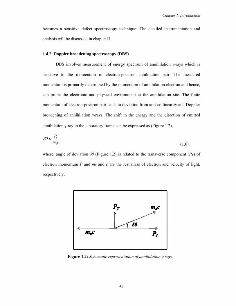
Chapter I: Introduction
42
becomes a sensitive defect spectroscopy technique. The detailed instrumentation and
analysis will be discussed in chapter II.
1.4.2. Doppler broadening spectroscopy (DBS)
DBS involves measurement of energy spectrum of annihilation γ-rays which is
sensitive to the momentum of electron-positron annihilation pair. The measured
momentum is primarily determined by the momentum of annihilation electron and hence,
can probe the electronic and physical environment at the annihilation site. The finite
momentum of electron-positron pair leads to deviation from anti-collinearity and Doppler
broadening of annihilation γ-rays. The shift in the energy and the direction of emitted
annihilation γ-ray in the laboratory frame can be expressed as (Figure 1.2),
0
TPm c
δθ ≈ (1.6)
where, angle of deviation δθ (Figure 1.2) is related to the transverse component (PT) of
electron momentum P and m0 and c are the rest mass of electron and velocity of light,
respectively.
Figure 1.2: Schematic representation of annihilation γ-rays.

Chapter I: Introduction
43
The energy of photons in laboratory frame is given as,
1 (1 cos )2 T
vE Ecγ θ= ±
(1.7)
Therefore, the energy of annihilation photon can be written in terms of its rest mass
energy as (neglecting the small deviation),
20 0 2
LPE E E m c cγ δ= ± = ± (1.8)
where, PL is the longitudinal component of the momentum i.e. component along the
emission direction of annihilation photons (taken as z-axis). The Doppler broadened
spectrum corresponds to the longitudinal momentum density given by,
( ) . ( , , )x y z x yW E const p p p dp dpρ= ∫∫ (1.9)
where ρ is the electron momentum space density and z-axis is the line joining the detector
and source. The detailed instrumentation and analysis will be discussed in chapter II.
1.4.3. Coincidence Doppler broadening spectroscopy (CDB)
This technique involves measurement of both the annihilation γ-rays in
coincidence. The coincidence measurement offers better signal to noise ratio as compared
to conventional Doppler broadening technique, especially in the high momentum region
of the Doppler broadened spectrum. This facilitates identification of chemical
surroundings at the annihilation site by indexing the annihilation with core electrons that
contribute to the high momentum region. The technique also provides better energy
resolution as compared to conventional DBS.
1.4.4. Age-momentum correlation technique (AMOC)
This technique is the hybrid of two conventional positron annihilation techniques.
This technique involves correlated measurement of positron lifetime (positron age) and
momentum of the annihilating electron-positron pair. The correlated measurement

Chapter I: Introduction
44
provides time resolved information about the positron states, helping unambiguous
interpretation of data with respect to positron and Ps chemical reactions, positron trapping
etc. [Dauwe et al., 2003; Suzuki et al., 2003; Schneider et al., 1997].
1.5. Positron/Ps annihilation spectroscopy: A tool to probe condensed matter
PAS is a powerful technique to study variety of properties of condensed matter.
The atomic order sensitivity of positron/Ps and the propensity to get trapped in low
electron density regions (free volume hole, voids, vacancy defect etc.) enable PAS to
probe atomic and molecular properties in materials. The uniqueness of PAS arises from
the fact that annihilation γ-rays carry electronic information (density and momentum) of
the site of electron-positron annihilation. It is thus possible to investigate local structures
embedded in bulk of the materials like vacancies, dislocations, electronic structure of
defect, its size and concentration, superlattices and device structure. There are several
reviews on the application of PAS to study material properties [Siegel et al., 1980; Seeger
et al., 1974]. PAS has been extensively used to study variety of materials viz.
metal/alloys, molecular solids, semiconductors, polymers and biomaterials. In soft
condensed matter like polymers and biomaterials, o-Ps pick-off lifetime enables probing
the nanostructural properties viz. free volume distribution and correlated properties such
as glass transition, mechanical strength and stability [Ito et al., 1998, 1999a and 2000;
Bandzuch et al., 2000 and Mallon et al., 2003]. On the other hand, the obtained
momentum distribution (DBS, CDB, ACAR) together with positron/Ps lifetime helps in
the investigation of electronic structure, Fermi surface of materials [Smedskjaer et al.,
1998; Bansil et al., 1988 and Chan et al., 1992] and defects [West et al., 1973; Brandt et
al., 1983; Seeger et al., 1974]. PAS enables unambiguous identification and quantification
of vacancy defects, their charge states and electronic environment in semiconductors
[Gebauer et al., 2002; Slotte et al., 2003 and Krause-Rehberg et al., 1999; Tuomisto et al.,

Chapter I: Introduction
45
2007 & 2008]. Defect profiling and interfacial characteristics in semiconductor
heterostructures [Zubiaga et al., 2011; Makkonen et al., 2010] using PAS has emerged as
a novel technique for the investigation of nanostructural characteristics of semiconductor
devices. Beam based PAS is used as a porosimetry technique in wide range of
nanoporous films and membranes with an ability to provide pore architecture (pore
interconnectivity) and hidden porosity beneath dense layers [Gidley et al., 2006].
Characterization of porous materials of technological importance like zeolites, silica
[Miranda et al., 1993], aerogels [Miranda et al., 2006] etc. is another application of
porosimetry using PAS. In addition to the characterization of nanostructural properties of
materials, other physical properties pertaining to nanoscale confinement are recently
being studied using PAS. This includes phase behavior of liquids confined in nanocavities
[Dutta et al., 2006 and 2008] and glass transition temperature of polymer thin films
[Keddie et al, 1994; Dalnoki-Veress et al, 2001]. A review of general applications of
positron/Ps in probing molecular substances can also be found in literature [Jean et al.,
2003].
In the present thesis PAS has been used to probe nanostructural properties of
different kinds of nanoscale materials. The main aim is to explore the effect of reduced
size on the structural and related properties of nanoscale materials. An introduction to
nanoscale materials, their properties and characterization tools is described in the
following section.
1.6. Nanoscale materials
Nanoscale materials are defined as the materials with at least one dimension
restricted to nanometer length scale (~ 100 nm) and possess unique optical, electrical and
magnetic properties. Within this length scale, properties of materials (such as strength,
resistivity, conductivity etc.) are significantly different than their bulk counterparts owing

Chapter I: Introduction
46
to the dominant role of surface energy. With the advancement in science and technology,
especially towards miniaturization of electronic devices, manipulating matter at the level
of atomic orders and characterization of the properties at nanoscale has gained intense
interest in the last two decades. The characterization and understanding of material
properties is of utmost importance in order to develop new materials with potential
applications in the area of science, engineering, technology and medicines. Nanoparticles,
semiconductor nanocrystals, porous materials (fullerenes, cabon nanotubes and fibres,
zeolites, silica, metal organic frameworks etc.) and thin films (~ few nm thickness) are
few of the many examples of nanoscale materials. Some of these nanoscale materials are
already being commercially available for many applications in industry and medical
sciences. In addition to their technological relevance, these materials are topic of current
research for fundamental studies related to the effect of reduced dimensionality on the
properties of materials. In the present thesis work, the studied nanoscale materials are
categorized into two classes: (i) nanopores in porous materials and, (ii) nanoscale thin
films. The nanopores of porous materials are employed as confining geometry for
different liquids and the properties of liquids under nanoscale confinement is the main
subject of study under porous materials category. Pore structure of porous materials
dictates various properties of the material like transport and permeability in membranes,
exchange capacity in zeolites etc. In this regards, pore architecture in porous membranes
in terms of pore interconnectivity has been investigated by making use of mobility of
positron/Ps in the medium (porous network). In the area of nanoscale thin films,
modification of nanostructure of organic semiconductor (OSC) thin films as a function of
different growth parameters and post growth annealing treatment has been studied. In
addition, defect depth profiling has been carried out to probe interfacial characteristics in
OSC heterojunctions as well as self-assembled monolayer (SAM) modified surfaces in

Chapter I: Introduction
47
organic field-effect transistors. A broader discussion on these aspects is given in the
following.
The study of properties of materials and their different phases has been an area of
fundamental research for decades. Confinement leads to significant change in material
properties as compared to its bulk owing to increased surface to volume ratio due to
reduced dimensionality. In this regards, study of properties of liquids confined in nano
sized cavities has attracted interest due to their significance not only for fundamental
research, but also for the advancement of technology especially in the areas related to
lubrication, adhesion, catalysis, fabrication of nanomaterials and nanotribology. It has
been observed that properties of liquids confined in nanodomains significantly differ from
their bulk properties. Confined liquids exhibit peculiar thermodynamic properties, shift in
freezing/melting behavior and existence of different phases. The interaction with the solid
surface organizes/put constraints on the confined liquid, thus, modifying physical
(density, layering, wettability with the surface etc.) and dynamical (relaxation, diffusion)
properties. Therefore, understanding the phase behavior of liquids in confinement is
desirable not only to understand fundamental physics behind the phase behavior (i.e. role
of surface interactions and size of confining geometry) but for their crucial role in various
biological and physical processes. Different techniques are being used to study structural,
dynamical and thermodynamical properties of confined liquids. Calorimetry (differential
scanning and adiabatic) are mainly used for the determination of heat flow and heat
capacity; Fourier transform infra-red, X-ray and neutron diffraction and scattering
techniques provide information about the structure and density of the confined phase
whereas, the dynamical properties are mainly studied using nuclear magnetic resonance
(NMR), solvation dynamics and dielectric relaxation spectroscopy (DRS).

Chapter I: Introduction
48
Apart from providing a confining region for liquids or other materials, porous
materials are important for catalysis, separation processes and ion exchange. Therefore,
characterization of porous materials is another important field in nanoscale technology.
Pores in the membranes act as sieve and govern transport and permeability properties of
the membranes. Tuning the membrane properties like pore size, porosity and chemical
nature can provide high selectivity and efficient permeability for separation processes.
These properties however, depend on the microstructural characteristics of the
membranes or pore architecture. Pore architecture refers to the quantification of pore size,
porosity and the length scale over which the pores are connected to each other. Therefore,
characterization of pore architecture of the membranes is essential in order to customize
membrane properties for variety of applications. Varieties of techniques are available to
characterize pores having their sensitivity to different length scales. Gas/solvent
adsorption is the most popular technique for the determination of pore size and
distribution. Among other techniques, small angle neutron scattering, ellipsometry
porosimetry and electron microscopy are being used to characterize size as well as pore
fraction. However, these techniques are limited by their sensitivity to hidden, closed and
interconnected pores.
Thin film technology is pervasive in many applications, including
microelectronics, optics, magnetic, hard and corrosion resistant coatings, micro-
mechanics, etc. Thin films (single and multilayers) are basic building block of all the
electronic devices like solar, photovoltaic cells, transistors, light emitting diodes etc. The
ability to selectively and controllably deposit thin films and characterization of
morphology/nanostructure of the films is a prerequisite in order to develop devices with
specified electronic and optical properties. The structure and morphology of the film play
key role to ascertain working mechanism and performance of the device. In this regards,

Chapter I: Introduction
49
defects (vacancy, lattice, structural defects like grain boundaries etc.) are seen to
influence charge transport and optical properties of the device. For example, these defects
act as charge traps and recombination centers thus, reducing the efficiency of the device.
Different growth parameters like the nature of substrate, deposition temperature,
deposition rate etc. are seen to influence nanostructure of the grown film. Different
nanostructural configuration (nanorods, nanocrystals, nanoribbons etc.) can be achieved
by the combination of different growth parameters and deposition techniques. These
nanostructural characteristic (configurations and orientation of grains) can be tailored to
achieve high efficiency and better performance of the devices. In addition to structure and
morphology of the film, interfaces between various components of the device are also
crucial for device performance. Heteroepitaxy between different materials leads to
structural defects or disorder at the interfaces which influence the charge transport and
light absorption/emission characteristics of the device. Therefore, control over growth
mechanism and characterization of structural properties is crucial for the development of
efficient and high performance devices for technological applications. Surface
morphology of thin films is mainly characterized by atomic force and scanning electron
microscopy whereas, structural properties like lattice structure of the grown film is
investigated using X-ray diffraction/grazing incidence X-ray diffraction. Depth dependent
structural properties are mainly studied using X-ray reflectivity, near edge X-ray
absorption fine structure, sputter-ion based X-ray photoelectron spectroscopy and
secondary ion mass spectrometry techniques.
1.7. Positron annihilation spectroscopy: Characterization tool for nanoscale
materials
PAS is a sensitive technique to probe atomic scale structural properties in
condensed matter. When a positron enters the solid, it loses its momentum rapidly and

Chapter I: Introduction
50
thermalizes within a few picoseconds. After thermalization, it diffuses for few hundreds
of picoseconds before finding an electron followed by annihilation. The gamma radiation
emitted after the electron-positron annihilation carries information about the electron
density and momentum distribution and thus, enables identification of various properties
of the material. The unique ability of positron to get trapped in low electron density
regions like voids, vacancies, open/free volumes etc. provides sensitivity to probe atomic
order defects in materials. The lifetime of positron/Ps at the trapping site can be
correlated to the size of the trap, whereas, Doppler broadening of annihilation gamma
radiation contains information about the chemical environment at the annihilation site.
Thus, PAS can be employed to probe structural characteristics in materials at nanoscales.
PAS is used to probe vacancy defects in metals/alloys and semiconductors and sub-
nanometer voids termed as free volumes in polymers. This provides an unambiguous
identification of vacancy clusters or nanocrystallites formed in metals/metal oxides and
nanostructural characteristics in polymers and polymer nanocomposites. This information
can be correlated to various physical, opto-electronic and thermal properties of materials.
The ability to get monoenergetic positrons (positron beam technique) has enabled
characterization of surfaces and depth profiling of microstructure in thin films. The image
potential well at the surface acts as a two-dimensional defect for positron and may trap
the positrons. This enables identification of structural imperfections (like steps, islands,
surface vacancy etc.) on the surface using low energy positrons. It is thus, possible to
characterize surfaces, especially at the nanometer scale where, finite size and reduced
dimensionality induced effects are predominant. Depth profiling using positron beam has
also opened a possibility to characterize buried interfaces in heterostructures as well as
characterization of modified interfaces. Defect free surfaces and interfaces are essential
for fabrication of all the electronic devices. With above mentioned capabilities, PAS has

Chapter I: Introduction
51
emerged out as a sensitive characterization technique in the area of nanoscience and
nanotechnology.
1.8. Scope of the present work
1.8.1. Nanodroplets
Nanodroplets refer to liquid confined in nano domain. Liquids under confinement
at nanoscale exhibit significantly different phase behavior/properties as compared to the
bulk. The introduction of surface forces, and the competition between fluid–wall and
fluid–fluid interaction, can lead to interesting surface-driven phase changes. The
fundamental scientific interest in this area is to understand the new physics that results
from finite-size effects, varying dimensionality, and surface forces. When the pore width
is of the order of the range of the intermolecular forces, a large fraction of the confined
molecules experience a reduction in the number of nearest-neighbour molecules, leading
to large shifts in phase coexistence curves and a lowering of critical points. Plenty of
experimental studies have been performed to address the science and phenomenon behind
the deviation of physical and thermodynamical properties of liquids confined at nanoscale
dimensions from their bulk counterparts. For this, different topics of condensed matter
physics have been considered in confined geometry including H-bonded liquids, polymer
physics, phase transitions, critical phenomena, and the glass transition temperature. In the
area of phase transition studies, freezing/melting behavior of confined liquids has been
studied extensively. It has been established that the first-order transition, i.e.
freezing/melting point (Tf), for a bulk material differs from that of the same when it is
confined in porous systems. The effect of size on Tf has been studied for organic
molecules [Jackson et al., 1996], metal particles [Couchman et al., 1977] and polymer
lamellae of different thicknesses [Cheng et al., 1987]. The observed shift in Tf has been

Chapter I: Introduction
52
explained from classical thermodynamics Gibbs-Thomson relationship [Thomson et al.,
1871; Defay et al., 1966; Evans et al., 1987] given by,
( )2 SW Lwf pore bulk
σ -σ TT =T -T
HρRΔ = −
(1.10)
where, σSw and σLw are the interfacial free energies per unit area for the solid-wall and
liquid-wall interfaces, respectively, H is the melting enthalpy of the solid, ρ is its density
and R is the radius of the confining pore. However, this classical relationship breaks down
for small pores, as the concept of surface tension is not well defined and the bulk values
of melting enthalpy and density of solid may no longer be valid in small size pores. In
addition to the shift in Tf, direction of the shift i.e. elevation or depression in Tf, has also
been observed. The direction of shift depends upon whether the pore wall favours the
confined solid phase or confined fluid phase. If the solid-wall interfacial free energy (σSw)
is higher than liquid-wall interface (σLw ) then, ∆Tf is negative or, depression in
freezing/melting temperature is observed and vice-versa [Miyahara et al., 1997;
Radhakrishnan et al., 2002]. There are number of experimental studies employing variety
of techniques such as differential scanning calorimetry [Zheng et al. 2007], nuclear
magnetic resonance [Kimmich et al., 2002], dielectric spectroscopy [Barut et al., 1998],
neutron scattering [Alba-Simionesco, et al. 2003] etc. and a range of confined systems to
explore the effect of pore size and role of fluid-wall interaction energy on the
shift/direction of freezing/melting point. In addition to experimental studies, subsequent
molecular dynamics studies [Miyahara et al., 1997; Radhakrishnan et al., 2002] have also
shown that Tf is strongly affected by the strength of attractive interaction between the
liquid molecules and the pore wall.
In the light of the reported experimental results and molecular dynamics
simulations on the phase transition behavior of confined liquids, we have employed

Chapter I: Introduction
53
positron/Ps annihilation spectroscopy to investigate the freezing/melting behavior of a
variety of liquids confined in different nano geometries. The main objective of the work
is to understand the role of confining geometry as well as the surface interactions between
the liquid and wall of the confining geometry on the phase transitions of confined liquids.
PAS has been used to study the phase behavior of number of gases and liquids confined
in porous materials [Duffy et al., 2000; Bartos et al., 2001; Wilkinson et al., 1992] and
mobility of glass forming liquids under confinement effect [Kilburn et al., 2008]. Bristol
positron group has studied the phase diagram of CO2 confined in vycor glass [Fretwell et
al., 1996]. Our positron group has also been involved in the studies related to the phase
transition of different liquids confined in silica and zeolites for the past few years [Dutta
et al., 2006 and 2008]. In all those studies, the main focus was on the effect of pore size
on the freezing/melting point of the liquid (benzene) confined in silica and zeoilte pores.
The depression in freezing/melting point of benzene was observed in both silica and
zeolite pores. However, the extent of the shift was seen to be different depending upon
the size of the pore. The negative shift observed in the pore was attributed to the slightly
repulsive interaction of benzene with the pore walls. In continuation with these studies, to
examine the role of interactions between the liquid and wall of the confining geometry on
the phase transitions of confined liquids, two other liquids viz. ethylene glycol and
isopropanol confined in zeolite nanopores has been studied in the present work. These
two liquids experience attractive interaction with the pore walls through hydrogen
bonding between the liquid and the -OH group at the wall of the zeolite pore. As a result,
an elevation in freezing/melting point was observed in both the liquids. However, the
strength of the fluid-wall interaction is different due to the distinct nature of hydrogen
bonding in these liquids. As a matter of fact, iso-propanol [CH3CH(OH)CH3] has inter-
molecular hydrogen bonding and strong attractive interfacial interaction with the pore

Chapter I: Introduction
54
surface whereas, ethylene glycol [(CH2OH)2] experiences both intra- and inter-molecular
hydrogen bonding, resulting in reduction in the strength of interfacial interaction towards
the surface. The difference in the extent of fluid-wall interaction resulted in the different
amounts of shift in the freezing/melting point in the two cases. The elevation in
freezing/melting point of these liquids as revealed from PAS was corroborated with the
NMR studies, wherein, spin-spin relaxation time was indexed to investigate the dynamics
of the liquids. The sensitivity of relaxation process to the mobility of the molecules
embodying the spins and hence, the intermolecular interactions can provide information
about temperature mediated structural and dynamical changes in the liquid. The structural
and dynamical information can then be used to index phase transitions.
In addition to shift in freezing/melting point of the liquids, thermodynamic
properties (latent heat capacity, enthalpy), structural and dynamical properties (shear
viscosity, mobility) also show deviation from the bulk behavior. There are experimental
reports on the investigation of structure of confined phases using NMR and X-ray/neutron
diffraction techniques, whereas, the dynamical properties have been studied using DRS,
neutron scattering, solvation dynamics and NMR techniques. In this regards, nanoscale
confinement of water has attracted considerable attention due to its relevance to
fundamental physics, biological and geological processes as well as technological
developments at nanoscale. For instance, water molecules confined in nanocavities of
biomolecules play crucial role in regulating molecular structure [Zhou et al., 2004]. In the
field of nanotribology and nanofluidics, behavior of molecularly thin water films
influences nanomechanical dynamics of water [Holt et al., 2006; Khan et al., 2010]. It has
been seen that nanoconfined water exhibits peculiar properties differing from the bulk. In
this context, study of structural and dynamical properties of confined water has been an
area of extensive research in order to understand the anomalous behavior of water in

Chapter I: Introduction
55
nanoscale confinement. A lot of studies have been carried out in the context of structure
and dynamics of confined water [Koga et al., 2001; Striolo et al., 2003; Mallamace et al.,
2007] using variety of techniques and confining matrices. These studies mainly concern
with the phase transitions and glass transition of water [Alba-Simionesco et al., 2006],
nature of crystalline phases of ice formed inside the pores [Hummer et al., 2001],
existence of disorder/amorphous regions within the pores etc. The anomalous behavior of
water in confined systems has been attributed to the effect of surface interactions which
modify the hydrogen-bonded network of water resulting in the formation of new phases
and emergence of transitions otherwise, not prevailing in the bulk. In this context, we
have studied structural and dynamical properties of water confined in saponite clay
nanopores which act as one dimensional confining domain (referred as 2D confined
water) using PAS, NMR and DRS. Water exhibits attractive interaction with the pore
walls owing to the existence of hydrogen bonding between the water molecules and the
silanol groups in addition, to the strong inter-molecular hydrogen bonding network. The
effect of interfacial interaction on the phase behavior of confined water has been probed
by indexing the variation in structure and dynamical properties. The comprehensive study
of structural and dynamical properties of confined water has shown the presence of two
transitions viz. above and below the bulk freezing temperature of water. This has been
attributed to the existence of distinct regimes of water inside the pores undergoing
transitions at different temperatures. The study has provided an insight into the structural
and dynamical changes in confined water pertaining to the role of interaction energies
between the water and the matrix. The presence of the transition at a temperature above
the bulk freezing point of water, in addition to a transition below the bulk freezing point
is the first report on the phase behavior of nanoconfined water.

Chapter I: Introduction
56
Experimental and theoretical work in the area of confinement i.e. phase behavior
in pores are beset with significant difficulties. On the experimental side, the morphology
of confining matrix i.e. poor knowledge of the exact distribution of pore size, shapes,
connectivity impose difficulties in the interpretation of the observed data. On the other
hand, in theoretical work, simulating the exact morphology of the porous material
considering the presence of impurities (might present in real system and can produce
spurious result) and the presence of metastable states leads to significant deviation from
the experimentally observed results. Despite a wealth of research, the overall view of the
phenomena prevailing in the confined systems is still lacking. This field is experimentally
and empirically driven and a lot work needs to be carried out in order to attain complete
understanding of the effect of confinement. In the study of phase transitions in confined
liquids, PAS has emerged as a sensitive technique to probe electronic-structural
alterations following the phase transition.
1.8.2. Pore architecture of membranes
PAS is a well established and sensitive tool to characterize nanostructure in
polymers by providing information about the pore size, its distribution and fraction of free
volume nanoholes. These nanostructural properties are deterministic measures for various
thermo-mechanical properties of the polymeric systems. The triplet Ps state (o-Ps) plays
the key role in probing porous materials through its reduced lifetime and 3γ/2γ branching
ratio when it is trapped in the pores. The o-Ps pick-off lifetime can be correlated to the
size and distribution of pores using Tao-Eldrup equation and the fractional free volume, fv
in a polymer that can be calculated using average volume of nanoholes and o-Ps intensity
as,
fv = CI3<vf(τ3)> (1.11)

Chapter I: Introduction
57
where, C is a constant, I3 is o-Ps intensity and <vf(τ3)> is the average volume of nanoholes
[Wang et al., 1990]. In addition to this, another important aspect in the characterization of
nanoporous materials is to understand the pore growth mechanism which mainly deals
with the length scale over which the pores are interconnected depending upon the
porogen loading. This has important implication in the context of generation of porous
matrices for various applications where the amount of porogen loading dictates not only
the porosity but the network between the pores. The ability of Ps to diffuse within the
porous network can be utilized to investigate pore architecture of the materials. Pore
architecture refers not only to pore size and its distribution but, porosity (closed and open)
and pore interconnectivity. The positron/Ps diffuses into the pores by colliding with the
walls of the pores and annihilates therein. The annihilation profile in the material can
provide information regarding the positron dynamics (diffusion) within the porous
network. The annihilation characteristics i.e. S-parameter and 3γ/2γ branching ratio as a
function of implantation energy of positrons are employed to evaluate positron/Ps
mobility in the material taking into account its diffusion, trapping and annihilation. The
mobility of positron/Ps is the direct measure of its diffusion length which can be
correlated to the length scale of pore interconnection i.e. pore interconnectivity. These
features of PAS have been used in the characterization of porosity in large variety of
technologically relevant nanoporous materials. For example, porous structure in low-k
dielectric thin films for microelectronics applications where control over porosity is one
of the crucial factors in deciding the high speed and high integration chips for
miniaturization of devices [Lynn et al., 2006; Gidley et al., 2007; Sun et al., 2002, Petkov
et al., 2001]. In the area of membrane science, characterization of pore architecture of
membranes used in separation science [Wang X. Y. et al., 2006], filteration
[Baerdemaeker et al., 2007] and pervaporation [Huang et al., 2008] applications, is

Chapter I: Introduction
58
crucial to determine the permeability and transport properties of the membrane. These
studies have explored pore structure in terms of pore size, open and closed porosity, pore
interconnectivity in membranes and thin films, pore structure analysis of hidden layers
and asymmetric membranes that are otherwise, inaccessible to solvents and gases and
characterization of multilayer films. Most of the PAS studies on the characterization of
pore structure are focused on the identification of nanopores/nanoholes. In the present
work, PAS has been utilized for the characterization of pore architecture in mesopores
membranes (micron size pores). Though, PAS is not sensitive for the determination of
micron size pores in the materials, however, Ps dynamics in the porous network can be
utilized to analyze microstructural properties in the mesoporous systems. In this respect,
Ps diffusion length is a sensitive index for the determination of length scale of pore
interconnection (pore interconnectivity) in the membranes. In the present work, Ps
diffusion length in supported liquid membranes (PTFE) and track-etched polycarbonate
membranes with varying pore sizes in the range of microns has been calculated from the
measured 3γ/2γ ratio as a function of positron implantation depth. Porosity at the surface
has been measured by comparing 3γ/2γ ratio at lower implantation energies (surface
region) as well as Ps diffusion length in pristine and gold capped membranes. Gold
capping at the surface prevents Ps from escaping from the surface of the membrane. A
large difference in 3γ/2γ ratio in the two cases is an indication of high open porosity and
vice-versa. Pore interconnectivity together with porosity at the surface has provided a
comprehensive picture of the pore structure in the studied mesoporous membranes. The
measured pore architecture (pore interconnectivity/Ps diffusion length) of these
membranes is then correlated with the permeability and transport properties of the
membranes. The study has provided a new approach to utilize PAS for the

Chapter I: Introduction
59
characterization of mesoporous membranes as well as identification of closed and
interconnected pores present in the materials.
1.8.3. Nanostructure characterization in organic semiconductor thin films
Thin films of nanometer thickness constitute one of the classes of nanoscale
materials. Similar to the case of confined fluids, properties of nanoscale thin films also
differ from their bulk forms. The interaction between the substrate and the constrained
thin film contribute to the observed differences in the properties. As an example, the
change in Tg of free standing ultra thin polymer films [Forrest et al., 1996; Keddie et al.,
1994] as well as supported polymer films [Jain et al., 2002] has been observed from
plenty of studies. The constrained dynamics of molecular chain has been assigned as the
main reason for the observed difference in Tg. In addition to the relaxation dynamics and
thermo-physical properties of thin films, the structural and morphological properties are
also observed to be affected due to the interaction potential/energy of the substrate. With
the advancement in the area of science and technology, especially in microelectronic
industry, thin films technology has emerged as the basic building block for all electronic
devices. Miniaturization demands components of nanoscale dimensions. The structural
properties hold the key role in dictating various properties and hence, performance of the
devices. For example, defects control many optical and electronic properties in
semiconductors, current density in superconductors, charge transport properties in
materials etc. Therefore, for high efficiency and high performance devices, control over
structural and morphological aspects is a prerequisite. The structure and morphology of
nanoscale films are highly dependent on the deposition techniques and conditions (nature
of substrate, its temperature etc.). In addition, interfaces between the various components
of the device are crucial for its performance and hold the key to ascertain the working
mechanism. For example, nature of interface determines the fate of excitons to be either

Chapter I: Introduction
60
stabilized (for efficient LEDs) or destabilized (for efficient PVs) at the interface.
Interfacial defects may act as traps for charge carriers and affect (lower) the conductivity.
The structural characterization plays a pivotal role in thin film research and essential to
realize perspectives for the next generation electronic industry. Thus, there is a need for
fundamental understanding using nanoscale characterization techniques to probe bulk,
surfaces, sub-surfaces and interfacial regions in thin films. There are numerous surface
analytical methods for the characterization of surfaces and sub-surface regions like
sputter-ion based X-ray photoelectron spectroscopy, secondary ion mass spectrometry
etc. However, these techniques possess the limitation of being destructive in nature.
In this context, slow positron beam based spectroscopy has emerged as a sensitive,
non-destructive defect characterization technique for nanoscale films. Implantation of
monoenergetic positrons into the materials helps in probing the surface, sub-surface
regions and buried interfaces. Together with the sensitivity of positron to defects of
atomic order in materials has made beam based PAS a novel characterization tool in the
area of thin film technology. There has been a plethora of work related to defect
characterization in semiconductor thin films (single and multilayers) [Zhao et al., 1996;
Brauer et al., 2002; Ferragut et al., 2010], thin high k-dielectric films on Si substrates
[Uedono et al., 2007], metal-oxide semiconductor (MOS) [Uedono et al., 1988] and
Si/SiO2 interfaces [Kauppinen et al., 1997]. The vacancy defects, structural defects like
grain boundaries and free volume, positron kinetics at the interfaces between different
materials are some of the properties probed using slow positron beam spectroscopy. All
these work relate to silicon or compound semiconductors materials.
In the present work, slow positron beam based spectroscopy has been utilized for
microstructural characterization of nanoscale organic semiconductor (OSC) films. In
contrast to the previous studies on inorganic semiconductors thin films, the present work
Chapter I: Introduction
61
is the first report on the microstructural characterization of sub-surface regions and
interfaces in nanoscale OSC films. The field of organic electronics has developed vastly
in the past two decades due to its promise for low cost, light weight, flexible, versatility
of chemical design and synthesis and ease of processing. However, charge mobility in
OSC materials is far lower than the inorganic ones. Therefore, efforts are being made to
achieve best possible mobility in these materials. Analogous to conventional inorganic
semiconductors, the performance of OSC devices (organic field-effect transistor, organic
light emitting diodes, photovoltaic cells etc) is directly related to structural properties like
molecular packing, crystallinity, growth mode and purity. Various properties of organic
devices viz. charge carrier mobility and opto-electronic property are highly dependent on
the properties of both the active layer (OSC) and the interfaces between various organic
and inorganic components of the devices. Since most of the organic molecules have large
anisotropy in their shape and structure, good quality film is a challenge and essential in
order to make best use of these molecules for organic electronic devices. The growth
mode and orientation of molecules depends on the interaction between the substrate and
the molecules as well as between two molecules. There are studies indicating the
detrimental effect of structural defects on the opto-electronic properties of the devices
[Zanfolim et al., 2010]. Therefore, in order to achieve best possible performance, it is
critical to understand and characterize growth and nucleation modes of organic molecules
under different conditions. In addition to molecular packing/orientation in active layers,
interface properties are also crucial for high efficiency and stability of the devices. The
charge transport across the interface between various organic and inorganic components
(e.g. source/drain in OFETs) and light absorption/emission (OLEDs) characteristics of the
device are believed to be influenced by structural and electronic properties of the
interface. Interfacial properties can be tailored by wettability or adhesion between

Chapter I: Introduction
62
different materials or modifying the electronic structure of the materials. For example, the
dielectric interface (between dielectric and organic layer) is modified by polymers or self-
assembled monolayers (SAM) which has influence on the growth behavior of OSC
molecules. In the context of characterization of organic devices, depth profiling using
slow positron beam has great potential owing to its capability to probe sub-surface
regions and buried interfaces at nanoscale. Depth profile studies using slow positron
beam open an avenue for the characterization of interfaces without the need of gate
electrode in the case of electronic devices.
The present study mainly concentrates on the investigation of nanostructural
variations as a function of varying deposition conditions (nature of substrate, deposition
temperature and post deposition annealing) and the defect structure at the interfaces
between different organic and inorganic components of multilayer heterostructures. Depth
profile study in the case of single layer films has shown the influence of the nature of
substrate and deposition temperature on the growth morphology of metal Phthalocyanine
films. The S-parameter and positron diffusion length have been indexed to examine the
structural variations. Defect depth profile study has indicated the presence of structural
inhomogeneities across the depth in the case of annealed OSC films. Post deposition
annealing is expected to improve the nanostructure (ordering of molecules) of the room
temperature grown film. Deposition at lower temperatures is required in the case of
materials which can decompose at higher temperatures. The study have indicated that
post deposition annealing may not provide a defect free microstructure/homogeneously
ordered films. Another interesting observation is the charge carrier mobility (determined
from current-voltage characteristics) in OSC films which is seen to be comparable to
positron mobility, evaluated from the diffusion length of positron in the films. Though the
scattering mechanism of electron and positron are different, the dependence of mobility

Chapter I: Introduction
63
(in both the cases) on structural defects enables comparison between the mobilities of the
two particles. This property can be used to get a prior idea of the charge transport
characteristic of the device by measuring the positron mobility in thin film without the
actual device configuration (electrode deposition). In the case of heterostructures
(different OSC materials viz. p- and n-type), the interface between organic-organic and
inorganic-organic materials dictates charge conduction. The epitaxial relation between
different materials results in structural defects which affects the conduction of charge
across the interfaces. The ability of positron to get trapped in defects as well as at the
interfaces has helped in characterizing interfaces in nanometer thin heterostructures.
Possible effect of electric field present at these interfaces (especially organic-organic) has
also been examined. In organic field-effect transistor, interface between the dielectric
material and OSC is critical for the charge conduction between the source and drain.
Dielectric surface modification allows controlling the structure and morphology of OSC
film and the interfaces. The structural characteristics (defects/morphology) of the
interface of the OSC film grown on silicon substrate with native and thermally grown
oxide (SiO2/Si) as well as surface modified SiO2/Si have been studied. The influence of
surface roughness on the structural characteristics of the grown films as well as interfaces
has been examined.

Chapter II: Experimental Techniques and….
64
CHAPTER-II
Experimental Techniques and Data Analysis
(Positron annihilation spectroscopy)

Chapter II: Experimental Techniques and….
65
Techniques in Positron annihilation spectroscopy
PAS comprises of different techniques which provide information about various
properties of the material through energy and time domain measurements of annihilation
γ-rays. These techniques differ primarily in the manner of detecting the γ-rays and
subsequent analysis of the spectrum. Positron lifetime spectroscopy (PALS), Doppler
broadening spectroscopy (DBS), Coincidence Doppler broadening spectroscopy (CDB),
Age-momentum correlation (AMOC) and 3γ/2γ annihilation spectroscopy are the
techniques in PAS. The conventional measurements using 22Na source provide bulk
information about the material whereas, depth dependent properties can be studied using
slow positron beam. In this thesis, conventional PALS and DBS techniques are used for
the study of phase transitions in nanodroplets and beam based DBS is mainly used for the
study of microstructure of thin films and porous membranes. Details of these techniques
and corresponding data analysis are described in this chapter. Other techniques used in
the present thesis work include Nuclear magnetic resonance, dielectric relaxation
spectroscopy, electrical conductivity (current-voltage) measurement, X-ray reflectivity
and conventional characterization techniques viz. differential scanning calorimetry,
Fourier transform infra-red spectroscopy, grazing incidence X-ray diffraction,
thermogravimetric analysis and atomic force microscopy. These techniques are described
in the relevant chapters.
2.1. Positron sources
2.1.1. Conventional techniques
The most suitable and widely used choice for conventional measurements is radio-
isotope based sources. The choice of the source depends upon which PAS technique is
used. 22Na is the most common choice of radioisotope positron source in PALS and
AMOC due to its relatively high positron yield of 90.4%, fairly long half-life (2.57 years)

Chapter II: Experimental Techniques and….
66
and appearance of 1275 keV prompt γ-ray almost simultaneously with the emission of
positron that serves as start signal in the PALS and AMOC experiments. The decay
scheme of 22Na is shown in Figure 2.1 [Firestone et al., 1999]. 22Na is not the best choice
for DBS as this technique does not require any prompt γ-ray which otherwise, adds to the
background counts. However, it is the most commonly used source for PALS and DBS
measurements.
22Na positron source has been obtained from the Board of Radiation and Isotope
Technology (BRIT), India in carrier free solution of 22NaCl. The solution of 22NaCl was
deposited drop by drop onto a 7.0 μm thick polyimide film (kapton®) till the required
activity is achieved and the active area gets dried. The active area was covered with an
identical film and edges were sealed with aluminium foil to prevent the leakage of
activity. The activity of source used in PALS and DBS measurements was ~ 10 μCi. The
positrons emitted from 22Na source have an energy distribution which ranges from zero to
0.54 MeV and has maximum at 0.19 MeV as shown in Figure 2.2. The implantation
profile of positrons in the sample is an exponentially decaying function based on
experimental observations. According to this, the intensity of positrons at a depth x in the
Figure 2.1: The decay scheme of 22Na

Chapter II: Experimental Techniques and….
67
sample is given by I (x) = I(0) exp(-αx), where α is the absorption coefficient of the
material for positrons and is given by 1.43 1max(16 1) E cmα ρ − −= ± [Brandt and Paulin, 1977].
Here ρ is the density of the material in g/cc and Emax (βmax) is in MeV. The mean
implantation depth of positron in the material is α-1. Therefore, the range of positrons
implanted into the sample has to be calculated prior its placement within the sample and
accordingly the thickness of the sample should be chosen. In the study of nanodroplets,
sealed source was embedded into the sufficient amount of powdered sample, ensuring no
escape of positrons from the sample.
2.1.2. Beam based techniques
For depth dependent measurements, positrons from slow positron beam were used
which can provide monoenergetic positrons of varying energies. In the present thesis
work, depth profile studies in organic semiconductor thin films (single and multilayer)
and characterization of pore architecture in porous membranes were carried out using
slow positron accelerator (beam) at Radiochemistry Division (SPARC), BARC, Mumbai
Figure 2.2: The positron energy spectrum in 22Na Decay

Chapter II: Experimental Techniques and….
68
(Figure 2.3). The beam facility is based on radioisotope 22Na (50 mCi) positron source.
The monoenergetic beam of positrons is obtained by the combination of moderator,
electric and magnetic field assembly and transported to the target chamber. The positrons
emitted from radio-isotope are moderated using 1 μm thick single crystal of tungsten, W
[0 0 1], which has negative work function for positrons and thus, provides positron of
energy equal to the work potential of tungsten. In the present beam, moderator is biased
to a positive voltage, 200 V and subsequent focusing via electrostatic Einzel lens and
transport with the help of magnetic field is optimized for 200 eV positrons. The focused
beam of positron from Einzel lens is made to transport to the target with the help of
magnetic field assembly comprising of bend solenoid and Helmholtz coils. The energy of
positrons is varied by the application of negative voltage to the target. This beam can
provide positrons in the energy range of 200 eV to 50 keV.
The implantation profile of monoenergetic positrons follows the Makhovian distribution,
given as,
Figure 2.3: Slow positron accelerator at Radiochemistry Division (SPARC), BARC, Mumbai.

Chapter II: Experimental Techniques and….
69
⎥⎥⎦
⎤
⎢⎢⎣
⎡⎟⎟⎠
⎞⎜⎜⎝
⎛−=
− m
omo
m
zz
zzmzP exp)(
1
(2.1)
where, zo is the function of positron incident energy and given as, zo = 1.13<z>, <z> is
mean implantation depth of monoenergetic positrons of energy E is given as,
nEAzρ
= (2.2)
where, <z> is the mean implantation depth (nm) and ρ is the density of material (g/cc).
The parameters A and n are material dependent constants. The parameters A and n are
usually taken as 40 and 1.6, respectively.
The positron thermalization and diffusion lead to the observed implantation profile
(Figure 2.4) which spreads from the surface to roughly twice the mean implantation
depth. Due to the spread in implantation profile at higher incident positron energies, best
resolution is achieved at low energies (shallow implantation depths).
2.2. Positron annihilation lifetime spectroscopy
2.2.1. Lifetime spectrometer
Figure 2.4: Positron implantation profile on a film of density 1 g/cc (figure taken from reference [Gidley et al., 2006]
Mean implantation depth

Chapter II: Experimental Techniques and….
70
The lifetime of positron in the material is measured by the distribution of the
events, each event being the time interval between the emission of 1.276 MeV photon
(birth signal of the positron), emitted almost simultaneously with the birth of the positron
and the emission of 0.511 MeV photon resulting from the annihilation of positron in the
medium using fast-fast coincidence setup. A schematic of the fast-fast coincidence setup
is shown in Figure 2.5. The fast-fast coincident setup employs a pair of scintillation
detectors along with photo multiplier tubes (PMT), two constant fraction differential
discriminators (CFDD), a time delay unit, a fast coincidence unit and a time-to-amplitude
converter (TAC).
The source sample assembly was kept between the two scintillation detectors. The
scintillators detectors are provided with photomultiplier tubes (PMT) for the processing
of the signal. The energy and timing information are obtained from the same output of the
PMTs using constant fraction differential discriminator (CFDD) unit. The 1276 keV and
511 keV γ-rays signifying the birth and annihilation (death) of positron, respectively, are
picked up by two scintillation detectors. The timing pick-off signals are communicated to
the TAC through CFDDs and the respective energy signals reach the coincidence unit
through the single channel analyzers (SCAs) of CFDD. The coincidence unit checks for
the ‘genuineness’ of the events and in the case of true coincident events, the TAC is
strobed by the output pulse of coincidence unit to produce a signal which is equivalent to
the time difference between the detection of 1276 keV and 511 keV γ-rays. The
magnitude of this signal is converted to pulse height and recorded in a multi-channel
analyzer [Pujari et al., 1992]. The time calibration of the multi channel analyzer was
chosen depending on the range of the lifetimes required to be measured. Most of the work
in this thesis required measuring Ps lifetime component (1-10 ns), therefore, time
calibration used was 25 ps/channel. The time calibration of the spectrometer was

Chapter II: Experimental Techniques and….
71
performed from the measured lifetime spectrum of 60Co γ-rays, keeping the discriminator
levels of the CFDDs same as required for positron lifetime measurements using a 22Na
source. The delay on the stop detector signal was varied systematically using a nano
second delay unit. The centroids of these peaks were plotted as a function of delay time
introduced on the stop detector and slope of this line gives the time calibration of the
spectrometer. The time calibration can also be calculated by dividing the TAC range (e.g.
50 ns) with number of channels in MCAs (e.g. 2K or 4K).
60Co emits the two γ-rays of 1173 keV and 1332 keV within a time of less than 1
ps. These two γ-rays are assumed to be emitted simultaneously and the peak shape of the
lifetime spectrum acquired for these two γ-rays is assumed to be Gaussian. The response
function (time resolution) of the spectrometer is obtained by measuring the time
difference between these two γ-rays. The lifetime spectrum of 60Co is shown in Figure
2.6. The time resolution of the spectrometer is estimated from the width of this peak. The
Figure 2.5: Block diagram of the positron lifetime spectrometer

Chapter II: Experimental Techniques and….
72
time resolution of present spectrometer was of the order 285 ps with BaF2 scintillations
detectors.
2.2.2. Lifetime spectrum analysis
Positron lifetime spectrum consists of sum of decaying exponentials convoluted
with the instrument’s time resolution function. Each decaying exponential represents a
positron state in the medium. Each spectrum consists typically a million counts to provide
sufficient statistics for the extraction of lifetime components. The positron lifetime
spectrum is given as,
( ) i
tk
i i
i eI
tF τ
τ
−
=∑=
1
(2.3)
where, F(t) represents the number of counts at time t, k is the number of exponential
decays, τi is the lifetime of the ith component, Ii is the corresponding intensity and B is the
constant background. The routine PATFIT-88 having programs RESOLUTION and
POSITRONFIT have been used for the discrete lifetime components analysis [Kirkegaard
et al., 1981 and 1989; Kirkegaard and Eldrup, 1972]. The positron lifetime spectrum
defined by Eq. 2.3 is convoluted with the resolution function of the spectrometer which is
Figure 2.6: The lifetime spectrum measured using 60Co γ-rays for obtaining the time resolution of the positron lifetime spectrometer.

Chapter II: Experimental Techniques and….
73
generally approximated by a sum of Gaussians or a Gaussian with exponential tails. A
single Gaussian distribution, G(t), centered at t0 is generally used for the deconvolution is
given as,
201( ) exp
22t tG tσσ π
⎡ ⎤−⎛ ⎞= −⎢ ⎥⎜ ⎟⎝ ⎠⎢ ⎥⎣ ⎦
(2.4)
where, σ represents the standard deviation of the Gaussian and is related to full width half
maximum (FWHM) of the Gaussian as,
2 2 ln 2FWHM σ= (2.5)
The convoluted lifetime spectrum is represented as,
2
00
1
4 1( ) .exp 12 2
ki i
i i i
t tI t tF t erf
στ
τ στ σ=
⎡ ⎤− −⎢ ⎥ ⎡ ⎤⎛ ⎞−⎢ ⎥= − − −⎢ ⎥⎜ ⎟⎢ ⎥ ⎝ ⎠⎣ ⎦
⎢ ⎥⎣ ⎦
∑
(2.6)
The count distribution in lifetime spectrum is integration of the time interval into one
fixed channel, represented as,
( ) ( )t t
t t
N t F t dt B+
−
= +∫ (2.7)
where, N(t) is the number of counts in the channel corresponding to time ‘t’, 2Δt is the
channel constant and B is the constant background. The value of σ is taken from the fitted
resolution function of 60Co spectrum or it is determined from a reference spectrum like
Silicon single crystal having a well defined positron lifetime (218 ps) using the routine
RESOLUTION. The background in the above model is taken as the average counts per
channel at the far end (no contribution from decaying exponential) of the lifetime
spectrum. A list of parameters τi, Ii, t0, σ and B is obtained after the analysis using
POSITRONFIT [Kirkegaard et al., 1989] model.

Chapter II: Experimental Techniques and….
74
Source correction
The positron annihilation in the kapton foil (sandwiching the source) and within
the source itself contribute to the lifetime spectrum and need to be subtracted from the
spectrum to get the lifetimes corresponding to positron states in the material. The
scattering of positrons from the sample also contributes to the fraction of positrons
annihilating within the source [Djourelov and Misheva, 1996]. The source correction for
the particular source used, can be calculated from the measured lifetime spectrum of a
silicon sample using routine RESOLUTION. The lifetime of positron in silicon is fixed as
220 ps and the other obtained positron components are taken as the source components.
For Kapton (7 µm thickness) one positron lifetime of 390 ps with 7 % intensity is
generally obtained. The source correction thus obtained is used in POSITRONFIT while
analyzing the actual lifetime spectrum of the sample.
2.3. Doppler broadening spectroscopy
2.3.1. Doppler broadening set up
A typical block diagram of Doppler broadening set up is shown in Figure 2.7.
DBS involves measurement of energy spectrum of 511 keV annihilation γ-ray. High
purity Germanium (HPGe) detector with best energy resolution has been employed for
Doppler broadening measurements. The annihilation signal is amplified by the
combination of preamplifier and spectroscopy amplifier and is fed into multi channel
analyzer (MCA). The MCA was energy calibrated using the standard multi γ-ray sources
of 152Eu and 133Ba. The energy resolution of the detection system was 2.0 keV at 1332
keV photopeak of 60Co. For each Doppler broadening measurement approximately half a
million counts were acquired under the 511 keV annihilation radiation.

Chapter II: Experimental Techniques and….
75
2.3.2. Data analysis
The Doppler broadened spectrum is generally convoluted with detector’s
resolution function (Gaussian function). However, for relative measurements, resolution
function need not be deconvoluted from the spectrum. In the present work, the
deconvolution of the detector resolution function was not carried out. The Doppler
broadened spectrum is characterized in term of line shape and wing parameters, which
contribute to low and high momentum distribution of the annihilation electrons,
respectively. The line shape parameter, S-parameter and wing parameter, W-parameter
were evaluated from the measured spectra using the program SP version 1.0 [SP-1]
[Dryzek, SP 1.0; Dryzek and Quarles, 1996]. The apparent background on left of 511 keV
is more compared to right, partly because of incomplete charge collection and scattering
in the sample. Additional background contribution comes from the Compton scattering of
1276 keV γ-ray. In this program, the background is taken as a step function. The S-
parameter is defined as the ratio of the central area (As) to the total area under the
spectrum (At) as,
Figure 2.7: Block diagram of Doppler broadening spectroscopy set up

Chapter II: Experimental Techniques and….
76
511
511
( )
( )
E
s E
t
N E dEASA
N E dE
+Δ
−Δ+∞
−∞
= =∫
∫ (2.8)
where, N(E) represents the counts in the spectrum at energy E. The W-parameter is
defined as the fractional area in the wing region of the Doppler broadened spectrum and
signature of the annihilations with core electrons of the surrounding medium. It is defined
as,
2 1
1 2
511 511
511 511
( ) ( )
( )
E E
E Ew
t
N E dE N E dEAWA
N E dE
− +
− ++∞
−∞
+
= =∫ ∫
∫ (2.9)
The values of ΔE, E1 and E2 for evaluating S and W-parameters were chosen in such a
way that the value of S-parameter is in the range of 0.50 or corresponding to 1.5 -1.9 keV
broadening of the annihilation peak and the value of W-parameter is in the range of 10-2
[Campbell, 1977]. A schematic representation of evaluating the line shape parameters in
the Doppler broadening spectroscopy is shown in Figure 2.8.
Figure 2.8: Schematic representation of evaluation of Doppler broadening parameters from DBAR spectrum

Chapter II: Experimental Techniques and….
77
S-W correlation analysis
The simultaneous analysis of S and W-parameter (S-W correlation) helps in
recognizing positron annihilation states in the materials [Clement et al., 1996]. The
correlated measurement of S and W-parameters is sensitive to type and the nature of
trapping site or defects in the material. Plotting S and W-parameters as a trajectory in the
S-W plane and using positron energy as the running parameter, provides a powerful
approach to interpret the depth profiling data especially in term of identification of
trapping layers [Asoka-Kumar et al., 1994].
3γ/2γ ratio analysis
The 3γ/2γ ratio is calculated from the annihilation spectrum of positron and Ps.
Annihilation into two photons (2γ) produces a peak at 511 keV and Compton scattered
events from 0-341 keV. However, annihilation into three photons (3γ) produces a
uniformly increasing energy distribution from 0-511 keV. Therefore, the total energy
spectrum is a combination of 3γ and 2γ events as shown in Figure 2.9. The 2γ and 3γ
contributions are evaluated from an energy window set around 511 keV and from the
integrated counts within an energy window 385-485 keV, respectively. The 3γ/2γ ratio
Figure 2.9: The energy spectrum of positron/Ps annihilation

Chapter II: Experimental Techniques and….
78
profile is a sensitive index to characterize pore architecture of porous membranes with
large size and interconnected pores [Gidley et al., 2006; Petkov et al., 2003].
2.4. Depth profiling using slow positron beam
Defect depth profiling in thin films (single and multilayers) and pore architecture
in polymer membranes have been studied using slow positron beam at Radiochemistry
Divison, BARC, Mumbai. Doppler broadening measurement has been carried out as a
function of positron incident energy to probe different depths of the samples. The energy
of the positrons was varied by applying required negative bias voltage to the sample. The
implanted positron follows Makhovian distribution in the sample [Schultz and Lynn,
1988]. The implanted positrons after thermalization, diffuse into the sample prior to the
annihilation. The average distance traversed by the positron before annihilation is termed
as positron diffusion length (L+) which can be correlated to the mobility of positron. The
positron mobility essentially refers to mean free path of positron in the system. The depth
dependent Doppler broadening measurement (S and W-parameters) and 3γ/2γ ratio were
used to evaluate positron/Ps diffusion length in the material. An HPGe detector having
30% efficiency and 2.0 keV resolution at 1332 keV (60Co) placed at 90o to the target
position and coupled to a 4k MCA was used for the measurements. The voltage applied to
the target was varied and Doppler broadening spectra at different positron energies
(implantation depth) were recorded. The line shape S-parameter calculated within ~ 2.0
keV energy window centered at 511 keV to the total photo peak area was evaluated as a
function of positron energy. The S-parameter as a function of positron energy is termed as
S-E profile of the sample. The wing parameter, W was evaluated from ~ 5.0 keV energy
window in the wing region of Doppler broadened annihilation peak. The S and W-
parameters with energy as a running parameter were used to get S-W correlation curve.
The ratio of 3γ/2γ annihilation was evaluated as a function of depth from the annihilation

Chapter II: Experimental Techniques and….
79
γ-ray spectrum. The ratio of integrated counts in the energy range 385 to 485 keV to total
area under the photo peak of 511 keV was used to calculated 3γ/2γ ratio. The variation of
3γ/2γ with positron incident energy gives information about the fraction of positron/Ps
reemitted from the sample at different depths. The curvature of S-E and 3γ/2γ profile is
used to evaluate mobility of positron/Ps in the material using variable energy fit analysis
(VEPFIT) as discussed in the next section.
2.4.1. Variable Energy Positron Fit (VEPFIT) analysis
The depth dependent characteristics can be obtained by extracting relevant
positron annihilation parameters as a function of depth or positron implantation energy.
This is achieved by fitting S-E or 3γ/2γ profile obtained from beam measurements using
VEPFIT analysis [van Veen et al., 1990]. It involves solving positron diffusion equation
(Eq. 2.10) taking into account the positron diffusion, trapping and annihilation in the
medium. The positron diffusion equation is given as,
2
2
( ) ( ( )) ( ) ( ) ( ) 0d t t bd c z dD v c z I z n c z c z
dz dz+ − + − κ −λ = (2.10)
where, c(z) is the time averaged positron density at a certain depth z below the solid
surface, vd is the drift velocity of positrons, I(z) is the positron stopping rate at depth z, nt
is defect density, κt is rate constant for positron trapping at defects, λb is the bulk
annihilation rate and D+ is positron diffusion coefficient. The drift velocity, vd = µξ, is the
function of electric field ξ present in the sample and mobility µ of positron in the sample.
The implantation profile of positrons is parameterized by Makhovian profile (Eq. 2.1).
The fast non-iterative calculation scheme is used to solve the diffusion equation to
calculate the time averaged positron density in the medium. The average positron density
is then used to extract diffusion length and the fraction of positrons annihilating at various

Chapter II: Experimental Techniques and….
80
depths taking into account various boundary conditions for the diffusing positrons. The
total fraction of positrons annihilating at a particular depth, Ti (Ek) given as,
( ) ijk
n
jjki tEPET ∑
=
=1
)( (2.11)
where, ti is the positrons that are surface-emitted or trapped in different depth intervals.
Using Ti (Ek) values, S-parameter as a function of positron energy Ek is defined as,
( ) surfsurfi
n
iik STTSES +=∑ (2.12)
Different models have been provided in VEPFIT analysis to fit the data for variety of
material characteristics. The choice of input parameters varies depending upon the model
chosen. In the case of thin films/heterostructures, Model # 5 is mainly used which can
provide S-parameter, L+ and layer thickness for each layer of the system. In the present
work, model# 5 has been used to fit S-E profile in organic semiconductor (OSC) thin
films wherein, multilayers were chosen to fit the data. This has not only provided positron
annihilation parameters in each layer but also, helped in the identification of interfaces
between various layers of the multilayer system. The inputs for the fitting analysis were
S-parameter as a function of energy (S-E profile), guess value of S-parameter, L+, layer
boundary and density of each layer. The semi-linear fitting procedure is carried out to fit
the experimentally measured S-E profiles through an iterative procedure. In the case of
pore architecture study in polymer membrane, instead of S-E, 3γ/2γ profiles were used for
the fitting procedure to obtain Ps diffusion length which was then correlated to pore
architecture of the porous membrane.
Other conventional characterization techniques like X-ray diffraction, Fourier
transform infra-red spectroscopy, thermogravimetric and evolved gas analysis and
differential calorimetric scanning have been used for nanodroplets study. The structural
and dynamical properties of confined fluids have been studied using nuclear magnetic

Chapter II: Experimental Techniques and….
81
resonance and dielectric relaxation spectroscopy. The experimental details are described
in chapter III. In the case of pore architecture study in membranes, scanning electron
microscopy has been used for surface characterization. The transport properties of the
membranes have been investigated from the permeability of Am+3 and Pu+3 ions through
the membranes. In OSC thin film study, atomic force microscopy and grazing incidence
X-ray diffraction have been used for the investigation of surface morphology and
crystallinity, respectively. The electrical properties have also been measured using
current-voltage (I-V) characteristics to calculate mobility of charge carriers in the films.
In addition to defect depth profiling using slow positron accelerator, electron density
profiling using X-ray reflectivity has also been carried out for the investigation of
nanostructure in organic semiconductor thin films. The experimental details are described
in chapter V.

Chapter III: Nanodroplets: Phase transitions…..
82
CHAPTER-III
Nanodroplets: Phase transitions in
nanoconfined fluids

Chapter III: Nanodroplets: Phase transitions…..
83
Nanoconfinement significantly affects structural and dynamical properties of the
fluids owing to the combined effect of reduced dimensionality, surface forces and finite
size. This includes nature of phase transition (first order vs. continuous), direction of shift
in freezing/melting point, origin of hysteresis, structural change of condensed phase and
effect on thermodynamical parameters. In this context, shift in the freezing/melting
behavior of fluids confined in nanodomains has been a subject of research for the last few
decades. Classical thermodynamics (Gibbs-Thomson equation) has been invoked to
explain the observed shifts in the freezing/melting point of confined fluids. However, in
the limit of small and highly inhomogeneous systems (nanopores), a deviation from
Gibbs-Thomson equation has been observed. This has been attributed to; (i) extremely
high surface to pore volume ratio, (ii) not well defined surface energy and, (iii) deviation
of melting enthalpy and density of the phases from their bulk values. Therefore, in
nanodomain, it is important to consider the surface/interfacial effects through a
description of the confined phase at the molecular level. The main stimulus behind the
ongoing research in the field has been to explore the effect of pore size, its geometry and
interfacial interactions on the properties of confined phases. In addition, emergence of
new phases/properties at nanoscale, otherwise not prevailing in the bulk has also attracted
the attention in this area.
Numerous studies have been carried out to explore the effect of pore size,
interfacial interaction between confining matrix and the confining phase. However, a
clear picture of the contribution of fluid-wall interaction separated from the finite size
effect on the freezing/melting properties has not been evolved in any of these studies. It
may be due to the reason that the relative contributions of geometrical confinement and
the fluid-wall interaction are difficult to separate. Also, the topology of the confining
matrix plays a crucial role in addition to these effects. Different techniques have been

Chapter III: Nanodroplets: Phase transitions…..
84
employed to study the phase transitions and properties of confined fluids. For example,
thermodynamic properties are mainly studied using calorimetry, diffraction techniques for
structure and density while scattering and relaxation spectroscopy for dynamical
properties. However, the existence of inhomogeneous phases, density variation and most
important, the small amount of sample (confined fluid) put limitation and complexities to
interpret the results. Hence, the comprehensive study using variety of techniques and
confining geometries are required to get better insight into the phenomena.
In this context, positron/Ps has emerged out as a sensitive and in situ probe to
study the phase behavior of confined fluids. Together with the ability of positron/Ps to
probe very small pores, the pick-off rate of o-Ps is sensitive to surface chemistry, change
of density and free volume following freezing/phase transition. When the pores are filled
with liquid, pick-off rate depends on the electron density as well as effective surface
tension of the confined fluid. In addition, when the volume fraction of the pores is high, a
significantly larger part of positron will interact with the liquid (or the solid, following
freezing) leading to an alteration in the intensity and life-time of o-Ps. Phase transitions
are manifested in the change in momentum distribution too, which can be indexed using
Doppler broadening S-parameter (solid and liquid state annihilation have different
momentum distribution). Free positron is also expected to behave like Ps and hence, can
be used to index phase transitions especially in the case when Ps yield is low.
In addition to positron annihilation spectroscopy (PAS), different techniques in
nuclear magnetic resonance (NMR) have also been widely used to monitor the dynamics
of fluid molecules trapped in the pores or adsorbed on surfaces. The dynamical
information can be utilized to study the phase transition behavior of confined fluid
molecules. The spin-spin relaxation time (T2) and chemical shift analysis are mainly used
to index phase transitions. The spin relaxation process is governed by the average

Chapter III: Nanodroplets: Phase transitions…..
85
distance between the spins, which, in a fluid, is determined by the state of mobility of the
molecules embodying the spins. In a porous medium, fluid molecules are in various states
of compartmentalization owing to various pore sizes, and their rigidity (mobility) is
affected in various degrees by the temperature of the surroundings. If the molecular
motion is fast, the effectiveness of spin-spin interaction is diminished, owing to the
averaging of the spin-spin dipolar interaction, and the resulting T2 is long. On the other
hand, when molecules are rigid, as in the pores whose size is comparable to that of the
molecules, or when the temperature is sufficiently low, the averaging is not so effective
and T2 becomes very short. T2 in fluid state is about two to three orders of magnitude
longer than that in the rigid or frozen state, if the pore size is sufficiently large compared
to the size of the molecule. If the majority of fluid molecules are in the state of high
mobility, the measurement of T2 yields an exponential decay of magnetization. On the
other hand, fluids bound in small pores often exhibit non-exponential decay arising from
a combination of different fluid components that are identifiable only by the states of
molecular mobilities they are in. Moreover, in the case of relatively rigid molecules, the
presence of strong dipolar interaction may also lead to a Gaussian decay. Hence,
relaxation time measurement is a sensitive probe to study the phase behavior of confined
liquid. In addition, the sensitivity of chemical shift to local magnetic field induced by
electronic currents surrounding the molecules is also used as an index to examine the
variation of intermolecular interactions and hence, can provide structural information.
The present study mainly aims at understanding the contribution of fluid-wall
interaction on the freezing/melting properties of confined liquids. Different techniques
viz. PAS, NMR and dielectric relaxation spectroscopy (DRS) have been used to
investigate structural and dynamical features associated with the phase behavior of
confined fluids. For this, two types of organic liquids viz. ethylene glycol and

Chapter III: Nanodroplets: Phase transitions…..
86
isopropanol, differing in the nature of hydrogen bonding were confined in ZSM 5
nanopores (pore size ~ 5Å). The strength of the interaction between liquid molecules and
the confining wall is different, but the topology and the pore size remain identical. Iso-
propanol [CH3CH(OH)CH3] has inter-molecular hydrogen bonding and strong attractive
interfacial interaction with the pore surface whereas, ethylene glycol [(CH2OH)2]
experiences both intra- and inter-molecular hydrogen bonding, resulting in the reduction
in the strength of interfacial interaction towards the surface. PAS and NMR have been
used to investigate change in the freezing/melting point of these liquids under the
nanoscale confinement.
The effect of confinement on the phase behavior of water confined in slit like
pores of saponite clay has also been studied. Water confined in a nanoscale environment
exhibits peculiar properties differing from the bulk such as confined water is unable to
grow into a crystalline structure and remains in liquid state becoming increasingly viscous
as temperature approaches glass transition. In such a metastable supercooled state,
anomalies in thermodynamic properties are seen, showing a power law divergence at a
singular temperature ~228 K. At very low temperature water can exist in amorphous
glassy form and show different amorphous phases depending upon the temperature and
pressure. The anomalous behavior of water in confined systems has been attributed to the
effect of surface interactions which modify the hydrogen-bonded network of water
resulting in the formation of new phases and emergence of transitions otherwise, not
prevailing in the bulk. Confinement of water in nano domains is therefore, sometimes
regarded as a trick to experimentally assess the bulk water properties within the
inaccessible low-temperature region and may provide answers to many open questions
concerning the properties of supercooled water. In addition, anomalous dynamical
properties have also been observed for supercooled water. In this context, cross over from

Chapter III: Nanodroplets: Phase transitions…..
87
non-Arrhenius to Arrhenius behavior at low temperature is a subject of intense debate.
Initially, this behavior has been assigned to fragile-to-strong transition (FST) of
supercooled water. However, recent studies have indicated that the existence of a
dynamic cross over is not restricted to water, but, other supercooled liquids as well
[Mattson et al., 2009; Hedstrom et al., 2007]. The structural α and β relaxations are also
invoked to explain the observed FST [Swenson et al., 2006].
Despite a wealth of research, complete understanding of the origin of such
anomalous behavior of confined water is still missing. Understanding the phase behavior,
as well as structural and dynamical properties of water, is complex and requires more
studies with a variety of confining matrices having a range of pore sizes and different
geometries. In addition to this, sensitivity of different techniques can be utilized for a
comprehensive study to probe properties of water confined in nanoscale. In the present
work, PAS, NMR and DRS together with other conventional characterization techniques
have been used to investigate the structural and dynamical aspects associated with the
phase behavior of water confined in clay nanopores (interplatelet space). The water
confined in interplatelet space is confined only in one-direction (say z-direction) and
allowed to move in the other two directions i.e. it can be considered as one-dimensional
confined system referred to as 2D confined water.
3.1. Sample preparation
3.1.1. Ethylene glycol and isopropanol confined in ZSM 5 zeoilte
Commercially available ZSM 5 zeolite (SiO2/Al2O3=30, surface area 380 m2gm-1
and pore volume 0.22 cm3gm-1) and analytical grade ethylene glycol and isopropanol
have been used. No dehydration of ethylene glycol was carried out. ZSM 5 zeolite sample
was heated at 573K under vacuum for 7-8 hours to remove adsorbed air and moisture. It
was cooled to room temperature and sufficient volume of ethylene glycol/isopropanol, as

Chapter III: Nanodroplets: Phase transitions…..
88
the case may be, was injected into the sample (in vacuum) with a syringe so that the entire
sample was covered with liquid. The liquid-sample mixture was kept overnight for
homogeneous adsorption of liquid into the pores. The sample was then evacuated at room
temperature using rotary pump for 10-15 minutes to remove the excess liquid /vapor at
bulk surface of the sample.
3.1.2. Saponite clay
Saponite clay containing Mg2+ as octahedral cations and Al3+ substituting Si4+ in
the tetrahedral sheet (Mg2+/Al3+/Si4+) has been synthesized using microwave assisted
radiation heating [Trujillano et al., 2011]. The saponite clay formula targeted was
[Si7MIII1] [MII
6] O20 (OH)4 [Na1]·n H2O, where MIII=Al+3, and MII=Mg+2. The mixture of
sodium silicate with divalent and trivalent cations was prepared in the molar ratios of:
Si/MII=7:6 and Si/MIII=7:1. The pH of the reaction mixture was maintained at 10.3 by
adding NaOH and NaHCO3. The resultant gel obtained was sealed in a 100 mL Teflon
reactor and treated hydrothermally in a microwave furnace at 180°C, for 7h. The
synthesized clay material was washed with de-ionized water to remove the unreacted
residues followed by drying at 80°C in oven. Saponite is a smectite type of clay having an
alumino-silicate layer structure where polymeric sheets of SiO44- tetrahedra are linked to
the sheets of alumina octahedra. The layers or sheets possess a net framework negative
charge, originating from the isomorphous substitution of Si4+ by Al3+ or Fe3+ in the
tetrahedral sheets, and by cation substitutions (e.g., Mg2+, Ni2+, Fe2+) in the octahedral
sheets. The net anionic framework charge on the sheets is compensated by the presence of
suitable charge balancing cations existing in their hydrated forms in interplatelet space.
The as-synthesized clay is the hydrated form with water confined between the
interplatelet spaces wherein, water is associated with the platelet surface and interplatelet
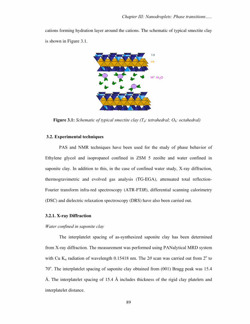
Chapter III: Nanodroplets: Phase transitions…..
89
cations forming hydration layer around the cations. The schematic of typical smectite clay
is shown in Figure 3.1.
3.2. Experimental techniques
PAS and NMR techniques have been used for the study of phase behavior of
Ethylene glycol and isopropanol confined in ZSM 5 zeoilte and water confined in
saponite clay. In addition to this, in the case of confined water study, X-ray diffraction,
thermogravimetric and evolved gas analysis (TG-EGA), attenuated total reflection-
Fourier transform infra-red spectroscopy (ATR-FTIR), differential scanning calorimetry
(DSC) and dielectric relaxation spectroscopy (DRS) have also been carried out.
3.2.1. X-ray Diffraction
Water confined in saponite clay
The interplatelet spacing of as-synthesized saponite clay has been determined
from X-ray diffraction. The measurement was performed using PANalytical MRD system
with Cu Kα radiation of wavelength 0.15418 nm. The 2θ scan was carried out from 2o to
70o. The interplatelet spacing of saponite clay obtained from (001) Bragg peak was 15.4
Å. The interplatelet spacing of 15.4 Å includes thickness of the rigid clay platelets and
interplatelet distance.
Figure 3.1: Schematic of typical smectite clay (Td: tetrahedral; Oh: octahedral)

Chapter III: Nanodroplets: Phase transitions…..
90
3.2.2. Thermogravimetric and Evolved Gas Analysis (TG-EGA)
Water confined in saponite clay
TG-EGA measurement was carried out using Netzsch Thermobalance (Model
No.: STA 409 PC Luxx) coupled to Bruker Fourier transform infra-red (FTIR) system
(Model No.: Tensor 27) via a heated Teflon capillary. Simultaneous TG-EGA
measurements were carried out individually on accurately weighed samples (about 100
mg) in inert atmosphere by heating from room temperature to 500 K at a heating
rate of 10 K min-1. The flow rate of high purity nitrogen was maintained at 100 mL min-1
to transport the volatile products. Nitrogen was also used as a protective gas to the
thermobalance at a flow rate of 20 mL min-1.
FTIR system used for the identification of evolved gases through the measurement
of IR absorbance in the mid IR region (400 – 4000 cm−1) was equipped with liquid
nitrogen cooled MCT detector and low-volume gas cell (8.7 mL) with a 123 mm path
length and KBr windows. The adapter head of thermobalance, transfer line and sample
cell were heated to a constant temperature of 473 K to avoid condensation of low volatile
compounds. FTIR compartment was continuously purged by high purity nitrogen and
molecular sieves/silica gel was used to minimize the water and carbon dioxide
background in the recorded spectra. The resolution of the collected spectra was set to 4
cm−1 and co-addition of 32 scans per spectrum with a scan speed of 20 kHz was applied.
As a consequence, spectra were recorded with a temporal resolution of about 2.5 s,
depending on the integration methods.
3.2.3. Attenuated total reflection- Fourier transform Infra-red spectroscopy (ATR-
FTIR)
Water confined in saponite clay

Chapter III: Nanodroplets: Phase transitions…..
91
A PIKE MIRacle™ Attenuated total reflection (ATR) accessory equipped with a
single reflection diamond ATR crystal was used for the analysis of solid samples. The
MIRacle accessory was fitted with a high pressure clamp, providing intimate contact
between the sample and ATR crystal. The MIRacle ATR accessory utilizes a pre-aligned,
pinned-in-place crystal plate design enabling easy exchange of ATR crystal for sampling
optimization. FTIR spectrometer (Bruker Tensor 27) was equipped with KBr
beamsplitter, DLaTGS (deuterated L-alanine doped triglycene sulphate) detector, sealed
and desiccated to minimize purge effects. The samples were placed over ATR crystal and
maximum pressure was applied using the slip-clutch mechanism. All spectra were
collected at 4 cm-1 spectral resolution using sample and background collection time of
one minute each. FTIR data analysis was done using Opus (version 6.0) software from
Bruker.
3.2.4. Differential scanning calorimetry (DSC)
Water confined in saponite clay
DSC measurements in temperature modulated and unmodulated (conventional)
mode were carried out in temperature range from 298-198 K. The conventional scanning
was performed by METTLER TOLEDO Thermal Analysis system using argon gas (flow
rate 60 ml min-1) in the DSC cell purge. The scanning speed was fixed at 2.0 K min-1. The
temperature modulated measurements were carried out using METTLER TOLEDO
Thermal Analysis system using argon gas (flow rate 60 ml min-1) in the DSC cell purge.
The system allows heating or cooling scans in the modulated DSC regime. The samples
were weighed and placed into standard Al sample pans with crimped lids. A matching
empty sample pan with crimped lid was used as the reference. The scanning was
performed by first cooling the samples from room temperature down to 198 K and then
starting the heating ramp to room temperature at a rate 2 K min-1. In order to obtain

Chapter III: Nanodroplets: Phase transitions…..
92
accurate and reproducible results, three experimental parameters, underlying heating rate,
modulation amplitude and modulation period were carefully selected. The modulation
period was varied from minimum value of 15 seconds to maximum value of 30 seconds
with modulation amplitudes of 1 K (+/- 0.5 K).
3.2.5. Positron annihilation spectroscopy
3.2.5a. Ethylene glycol and isopropanol
Temperature dependent positron lifetime and Doppler broadening measurements
were carried out in the temperature range from room temperature to 245 K in the case of
ethylene glycol and from 210 to 170 K in the case of isopropanol, in both cooling and
heating cycle. For low temperature measurements, the sample (powdered form and
hermetically sealed) along with the source (~8 μCi deposited on thin Kapton foil) was
mounted on the cold head of APD closed cycle helium refrigerator. Temperature variation
was carried out in 1 K interval with an accuracy of ±0.01 K. Doppler broadened
annihilation radiation measurements were carried out using an HPGe detector having
resolution of 1.8 keV at 1332 keV photo peak of 60Co. The shape parameter, namely, S-
parameter defined as the ratio of the number of counts falling in a fixed energy window
centered at 511 keV to the total number of counts, was evaluated. The experiments were
repeated in different samples (both cooling and heating cycle) and the reproducibility of
the data was seen to be good in both the liquids confined in zeolite. Positron annihilation
lifetime measurements were carried out using BaF2 scintillation detectors in a fast-fast
coincidence system. The time resolution measured with a 60Co source was 300 ps and the
time calibration was 25 ps per channel. Data analysis was carried out using PATFIT
program [Kirkegaard et al., 1981 and 1989; Kirkegaard and Eldrup, 1972].

Chapter III: Nanodroplets: Phase transitions…..
93
3.2.5b. Water confined in saponite clay
Low temperature positron lifetime and Doppler broadening measurements were
carried out in the same experimental set up (APD closed cycle helium refrigerator) and
the sample geometry as for ethylene glycol and isopropanol. The temperature variation
was carried out in the range of 200-300 K in both heating and cooling cycles. The
temperature variation was carried out in 2 K interval with an accuracy of ± 0.01 K.
Doppler broadened annihilation radiation measurements were carried out using an HPGe
detector having resolution of 2.2 keV at 1332 keV photo peak of 60Co and the variation of
S-parameter was measured. Positron annihilation lifetime measurements were carried out
using BaF2 scintillation detectors in a fast-fast coincidence system. The time resolution
measured with a 60Co source was 295 ps and the time calibration was 25 ps per channel.
Data analysis was carried out using PATFIT program.
3.2.6. Nuclear magnetic resonance
NMR measures the absorption of electromagnetic radiation during the transition
from spin states of atomic nuclei. In NMR experiments, a constant strong magnetic field
H leads to splitting of energy levels of the nuclei depending upon the spin states. The
energy difference between the two levels is given by,
πγ2hHE =Δ (3.1)
where, γ is a constant termed as gyromagnetic ratio of the nucleus defined as,
mq
2=γ (3.2)
where, q and m represent the electronic charge and mass of the nucleus, respectively. An
oscillating field B1 applied to the sample leads to absorption of energy, resulting in
excitation of the nuclei. The energy absorbed by a given nucleus, ∆E depends on the local

Chapter III: Nanodroplets: Phase transitions…..
94
magnetic field experienced by the nucleus. The local magnetic field is the resultant of
applied field and the field created by electron current in the molecular orbital. Therefore,
resonance frequency or ∆E depends on the electronic environment, and consequently on
the structural properties of the sample. The variation of interaction between the nuclei due
to any phase transition can be detected from the change in structural and dynamical
properties of the system which can be derived from chemical shift measurement and the
analysis of relaxation time.
3.2.6a. Chemical shift and relaxation time
The chemical shift (δ ) is defined as the variation of NMR resonance frequencies
of the same kind of nucleus, due to the variation of electronic distribution. It is measured
as the resonance frequency of the nucleus relative to a standard. The total magnetic field
experienced by a nucleus includes local magnetic field induced by the electronic currents
in the molecular orbitals which vary depending upon the local geometry (bond angle,
length, bonding partner etc.).
The radio frequency, RF (equal to the energy difference between the two levels)
applied to the sample causes spins to flip and redistribute among the two energy levels.
The energy absorbed by the nuclear spins induces a voltage that can be detected by a
suitably tuned coil of wire, amplified and the signal is displayed as free induction decay
(FID). The relaxation process eventually returns the spin system to thermal equilibrium,
which occurs in the absence of any perturbing RF pulses. The two relaxation processes
are; spin-lattice (or longitudinal relaxation time, T1) and spin-spin (or transverse
relaxation time, T2) relaxation. T1 measures how fast the magnetization relaxes back
along the z-axis, whereas, T2 measures how fast the spins exchange energy in the
transverse (xy) plane. There are several mechanisms by which molecular motions can
influence nuclear relaxation; direct interaction with the nearby nuclei (dipole-dipole),

Chapter III: Nanodroplets: Phase transitions…..
95
chemical shift effects, quadrupole interaction and j-j coupling. Different pulse sequences
are employed to measure relaxation times. Pulse sequence is the set of RF pulses applied
to the sample to produce a specific form of NMR signal.
In the present work, 90o FID pulse and spin-echo pulse sequences are used to
measure T2. In the 90o FID pulse sequence, net magnetization is rotated down into the xy
plane with a 90o pulse. The net magnetization vector begins to precess about z-axis. The
decay time is determined from the FID curve. The FID is an observable NMR signal
generated by non-equilibrium nuclear spin magnetization precessing about the magnetic
field direction. The non-equilibrium magnetization can be induced generally by applying
a pulse of resonance frequency (90o pulse as mentioned above) close to the Larmor
frequency of the nuclear spin. In the spin-echo pulse sequence, initial 90o pulse rotates
the magnetization into y-direction. Due to inhomogeneous magnetic field, spins fan out in
the xy plane with a loss of phase coherence. A 180o pulse applied after time τ, results in
phase coherence along the negative y-direction producing a signal called echo after time
2τ. Following the spin-echo, phase coherence will again be lost but can be regained with
another 180° pulse. T2 can be obtained from the amplitudes of the decaying echoes.
3.2.6b. Static and Magic angle spinning
NMR spectral lines obtained in static measurement from a liquid specimen are
much narrower than that in the solids. This difference in the behavior arises from the
static anisotropic interactions to which the nuclei are subjected in the solid state. By
contrast, in liquids the rapid isotropic motion of the nuclei average out the anisotropic
interactions and effectively remove them from the spectrum. These anisotropic
interactions include chemical shift anisotropy, dipolar coupling and quadrupole
interactions. The rotation/spinning of the solid specimen so as to mimic the rotation of
nuclei as in liquids can help in averaging out the anisotropic interactions in the solids.

Chapter III: Nanodroplets: Phase transitions…..
96
Rapid rotation about an axis inclined to an angle (magic angle) to the direction of
magnetic field can remove anisotropic part of chemical shift anisotropy and dipolar
coupling and a narrower spectrum can be obtained.
In a strong magnetic field, the dipolar coupling between the nuclei depends on the
orientation of internuclear vector with the applied magnetic field, given as,
)1cos3( 2 −∝ θD (3.3)
where, θ is the angle between the internuclear vector and the direction of applied
magnetic field and D is the dipolar coupling constant which tends to zero at θ = 54.7o
known as the magic angle. In the magic angle spinning measurement, specimen is
spinned at an angle of 54.7o with respect to field direction. In the present work, magic
angle spinning (MAS) has been used in the case of water confined in saponite clay. The
effect of MAS on improving spectral resolution is evident from the Figure 3.2.
Figure 3.2: One-Dimensional 1H spectrum of water confined inside clay nanopores, when the sample is static (grey) and spinning at 5 kHz at magic angle (black) inside the 700 MHz NMR spectrometer. The peak at 0 ppm in MAS spectrum corresponds to Si-OH group in the clay platelets. Peaks with stars on top of them are MAS side bands of the water and Si-OH peaks.

Chapter III: Nanodroplets: Phase transitions…..
97
3.2.6c. Ethylene glycol and isopropanol
1H NMR studies were carried out at a resonance frequency of 42.53 MHz with a
Bruker MSL100 NMR spectrometer and at 9.97 kOe using a field-dial controlled Varian
V7400 electromagnet. All the samples were sealed under argon atmosphere in glass tubes.
A Bruker temperature controller was used to vary the sample temperature. The spin-spin
relaxation time (T2) has been measured by Hahn-echo method using the pulse sequence
90°-τ-180° signal acquisition, which eliminates the effect of magnetic field
inhomogeneity on T2 decay. 90° pulse length was set at 2.1 μs and τ values were varied
between 0.5 – 30 ms. The intensity of the resonance spectrum for a particular component
of the fluid in which the nuclear spins experience a certain kind of interaction, is given
by,
( ) ( ) ( ) .2exp2
2
im
iTiIiI ⎟⎟
⎠
⎞⎜⎜⎝
⎛−=
ττ
(3.4)
where I2τ(i) is the intensity corresponding to the ith component of the resonance spectrum
after a time 2τ after 90° pulse, and mi is 1 for exponential and 2 for Gaussian decay. I(i)
are the fractional intensities of the components having spin-spin relaxation times T2(i).
The total intensity of the spectrum is given by,
( ) ( )∑=i
total iII ττ 22. (3.5)
T2 decay curves for ethylene glycol was decomposed into two distinct Gaussian decays
whereas, three Lorentzian decay curves were employed to decompose T2 decay curve in
the case of isopropanol.
3.2.6d. Water confined in saponite clay
Solid-state 1H NMR measurements were performed at a magnetic field of 16.43 T
(700 MHz of 1H Larmor frequency) using Bruker AVIII NMR spectrometer. 4 mm triple-
Chapter III: Nanodroplets: Phase transitions…..
98
resonance probe was used for static and MAS experiments. Clay samples in the form of
fine powder were packed in 4 mm rotors using ceramic caps to perform low temperature
studies. All chemical shifts were referenced with respect to 1H chemical shift of Si–OH
groups in clay fixed to 0 ppm at 298 K. Chemical shift of 79Br in KBr sample was used
for temperature calibration in static as well as spinning samples. The transverse spin-spin
relaxation time T2* (T2′) was measured in the temperature range 325-240 K. T2
* values
were calculated by measuring the full width at half maximum of water peak obtained
from 1D spectrum of static and spinning clay sample obtained with just a 90˚ pulse. T2′
measurements were carried out by monitoring peak height in 1D 1H spectrum of clay
recorded after a spin-echo. The observed 1H peak height was plotted as a function of spin-
echo duration to obtain transverse dephasing curves. These curves were then fitted to a
single-exponential decay function to obtain transverse dephasing times (T2′ values).
3.2.7. Dielectric relaxation spectroscopy
In dielectric relaxation experiments collective polarization of all the polar
molecules in the sample is measured. The dielectric relaxation time provides the measure
of the time taken by a system to reach the final polarization after an electric field is
switched on (or off). The technique measures the dielectric response i.e. complex
dielectric function ε*(ω) of the system under study. The complex dielectric function,
ε*(ω) can be decomposed into real and the imaginary parts as,
)()()( '''* ωεωεωε −= (3.6)
The real ε′(ω) and imaginary ε″(ω) parts represent the storage and loss part, respectively
for a relaxation process. Different molecular theories of dielectric relaxation process
provide microscopic understanding of the relaxation phenomena existing in the system.
The dependence of ε*(ω) on angular frequency originates from different factors, (i)

Chapter III: Nanodroplets: Phase transitions…..
99
microscopic fluctuations of molecular dipoles, (ii) the propagation of mobile charge
carriers (translational diffusion of electron, holes or ions), and (iii) the separation of
charges at the interfaces which give rise to additional polarization. The sensitivity of
dielectric relaxation to intermolecular interactions and its ability to monitor cooperative
processes at molecular level help in the investigation of properties of individual
constituents of the system and hence, derivation of macroscopic bulk properties.
3.2.7a. The dielectric constant and polarization
The static dielectric constant (relative permittivity) of a material is given by,
oCC
=ε (3.7)
where, C is the capacitance of a parallel plate capacitor with the space between the plate
filled with a dielectric material and Co is the capacitance with vacuum in between the
plates. The permittivity of the material depends on the polarisability of the molecules in
between the plate. The polarization of the medium is a function of frequency of the
applied electric field and is defined as,
EP o )1( −= εε (3.8)
where, εo is the dielectric permittivity of vacuum and is equal to 8.854×10⁻¹² Fm-1 and E is
the applied electric field. The total polarizability is the sum of electronic, atomic and
orientation (in case of polar medium) polarization. The applied field leads to polarization
of the medium by displacing the charge distribution/aligning the dipoles in a direction
parallel to the field. Each of these mechanisms has a characteristic resonant or relaxation
frequency.
3.2.7b. Relaxation Times

Chapter III: Nanodroplets: Phase transitions…..
100
Dielectric relaxation is a consequence of the movement of dipoles or electric
charges due to the changing electric field. Dielectric relaxation processes lie in a wide
range of characteristic times, 105-10-12 s and is denoted by,
max21
πντ = (3.9)
where, τ is the characteristic relaxation time and νmax is the resonance frequency of the
relaxation process. Relaxation processes are characterized by a peak in the imaginary part
(ε″) and a step-like decrease of the real part (ε′) of the dielectric function. The relaxation
processes are usually analyzed by using model functions. In the present work, a general
model function introduced by Havriliak and Negami (H-N function) [Havriliak and
Negami, 1966 & 1967], has been used to analyze the dielectric response of the system
under study. The H-N function is defined as,
( )( )[ ] ⎥
⎥⎦
⎤
⎢⎢⎣
⎡
+
Δ+= −
βαωτ
εωεσ
ωεi
n
o
DC
1Im" (3.10)
where, ω = 2πf, Δε = εS-ε∞, where, εS and ε∞ are static and high frequency limiting values
of the dielectric constant, respectively, σDC is the conductivity contribution, τ is the
relaxation time and n, α and β are empirical exponents with values between 0 and 1.
3.2.7c. Instrumentation and measurement technique
Using a sinusoidal electric field, E*=Eo exp(iωt) with angular frequency ω and at
field strength within the linear response (for most materials Eo ≤ 106 Vs-1), the dielectric
function is derived by measuring the complex impedance Z*(ω) of the sample, defined as,
oo CZiEij
)(1
)()(
**
**
ωωωωεωε == (3.11)

Chapter III: Nanodroplets: Phase transitions…..
101
where, j*(ω) is the complex current density. Fourier correlation analysis in combination
with impedance analysis has been used to evaluate amplitude and the phase of Z*(ω). The
schematic of the measurement technique is shown in Figure 3.3.
3.2.7d. Water confined in clay
For nanoconfined water in saponite clay, the dielectric measurements was
performed using a Novocontrol Alpha AN impedance analyzer over a frequency range of
10 Hz to 1 MHz at several temperatures in the range of 190-298 K. The sample in powder
form was placed between the two gold-coated electrodes in a parallel plate capacitor
configuration with a thin annular Teflon spacer for insulation. Sample was first cooled to
190 K and the measurements were performed while slowly bringing the temperature to
298 K using the Novocontrol Quatro nitrogen gas cooling/heating cryosystem. The
temperature was constant within ±0.5 K during each measurement of the dielectric
constant and loss. The similar measurement has been performed for dry saponite obtained
by heating the hydrated sample at 493 K in vacuum.
Figure 3.3: The schematic of the measurement of dielectric response

Chapter III: Nanodroplets: Phase transitions…..
102
I. Freezing/melting behavior of ethylene
glycol and isopropanol confined in ZSM 5

Chapter III: Nanodroplets: Phase transitions…..
103
3.3. Results and Discussion
3.3.1. Ethylene glycol and isopropanol confined in ZSM 5
3.3.1a. PAS results
The change in positron/Ps annihilation parameters (S-parameter, o-Ps pick-off
lifetime and intensity) as a function of temperature is indicative of phase transition. In the
present case, S-parameter, o-Ps pick-off lifetime (τp) and intensity (Ip) as a function of
temperature have been used to identify phase transition in ethylene glycol and
isopropanol confined in ZSM 5. The variation in S-parameter with temperature during
cooling and heating cycle for confined ethylene glycol is shown in Figure 3.4. It is seen
that during cooling cycle S-parameter initially decreases with the decrease in temperature
and a sharp discontinuity in S-parameter is seen around 270 K. Below 270 K, S-parameter
decreases and a second discontinuity is seen coinciding with the bulk freezing
temperature 260 K. In the heating cycle, interestingly, S-parameter change is significant
at the bulk freezing temperature and muted at 270 K. The temperature dependence of Ip
and τp for ethylene glycol are shown in Figure 3.5. Both these parameters show
discontinuities at 270 K and 260 K during the cooling cycle. The transition at 270 K may
be attributed to the freezing of ethylene glycol confined in nanoscopic pores (micropores)
of ZSM 5, which is 10 K above the bulk freezing temperature (260 K). However, the
values of τp in Figure 3.5 remain at about 1.1 ns both in liquid (above 270 K) and solid
(below 260 K) phase in contrast to ~2.3 ns expected in bulk liquid in this temperature
range. This implies either no bubble formation or the volume available for Ps trapping
must be similar in either phase. The origin of the available space may be the covolume
associated with ethylene glycol molecules. A gross average of ~26x10-3nm3 for the
covolume of a number of organic molecules would result in a life-time of 1.1 ns, in
excellent agreement with the measured o-Ps life-time. If the present correlation is correct,

Chapter III: Nanodroplets: Phase transitions…..
104
then it implies that the confined ethylene glycol molecules (i) are in an arrangement too
rigid for Ps to form a bubble and (ii) maintain their covolume over the temperature range
studied. The observed intensity of 15% at 280 K (Figure 3.5) in contrast to 22% in bulk
liquid suggests that either a large fraction of positron/Ps is localized in the liquid or there
is contribution from the zeolite bulk. However, the role of solvation phenomenon of
electrons in the liquid and its influence on the Ps yield cannot be ignored.
The pick-off intensity (Ip) response (in Figure 3.5) is observed to be quite different
from the response of S-parameter (in Figure 3.4). It is seen that unlike S-parameter, Ip
initially increases with the decrease in temperature till the discontinuity at the first phase
transition temperature 270 K. Immediate below 270 K, Ip shows a drop at 268 K, which
signifies the inhibition of Ps formation after the completion of liquid to solid phase
transformation in nanopores. Below 268 K, S-parameter is seen to decrease slowly till
260 K, which is essentially due to the behavior of liquid trapped in mesopores. At 260 K
(bulk freezing point of ethylene glycol), a second discontinuity in Ip, τp, as well as S-
Figure 3.4: The Variation of S-parameter with temperature during cooling and heating cycle for ethylene glycol in ZSM-5. The solid lines are for eye-guide.
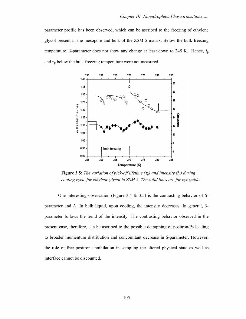
Chapter III: Nanodroplets: Phase transitions…..
105
parameter profile has been observed, which can be ascribed to the freezing of ethylene
glycol present in the mesopore and bulk of the ZSM 5 matrix. Below the bulk freezing
temperature, S-parameter does not show any change at least down to 245 K. Hence, Ip
and τp below the bulk freezing temperature were not measured.
One interesting observation (Figure 3.4 & 3.5) is the contrasting behavior of S-
parameter and Ip. In bulk liquid, upon cooling, the intensity decreases. In general, S-
parameter follows the trend of the intensity. The contrasting behavior observed in the
present case, therefore, can be ascribed to the possible detrapping of positron/Ps leading
to broader momentum distribution and concomitant decrease in S-parameter. However,
the role of free positron annihilation in sampling the altered physical state as well as
interface cannot be discounted.
Figure 3.5: The variation of pick-off lifetime (τp) and intensity (Ip) during cooling cycle for ethylene glycol in ZSM-5. The solid lines are for eye guide.
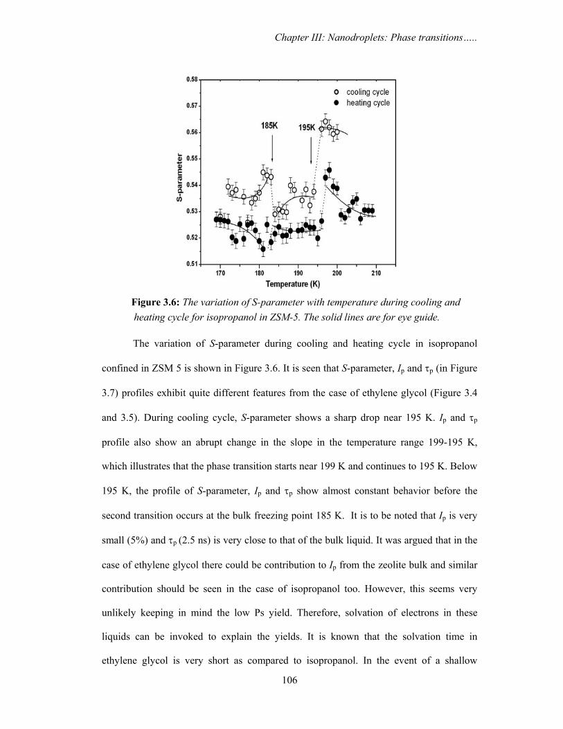
Chapter III: Nanodroplets: Phase transitions…..
106
Figure 3.6: The variation of S-parameter with temperature during cooling and heating cycle for isopropanol in ZSM-5. The solid lines are for eye guide.
The variation of S-parameter during cooling and heating cycle in isopropanol
confined in ZSM 5 is shown in Figure 3.6. It is seen that S-parameter, Ip and τp (in Figure
3.7) profiles exhibit quite different features from the case of ethylene glycol (Figure 3.4
and 3.5). During cooling cycle, S-parameter shows a sharp drop near 195 K. Ip and τp
profile also show an abrupt change in the slope in the temperature range 199-195 K,
which illustrates that the phase transition starts near 199 K and continues to 195 K. Below
195 K, the profile of S-parameter, Ip and τp show almost constant behavior before the
second transition occurs at the bulk freezing point 185 K. It is to be noted that Ip is very
small (5%) and τp (2.5 ns) is very close to that of the bulk liquid. It was argued that in the
case of ethylene glycol there could be contribution to Ip from the zeolite bulk and similar
contribution should be seen in the case of isopropanol too. However, this seems very
unlikely keeping in mind the low Ps yield. Therefore, solvation of electrons in these
liquids can be invoked to explain the yields. It is known that the solvation time in
ethylene glycol is very short as compared to isopropanol. In the event of a shallow
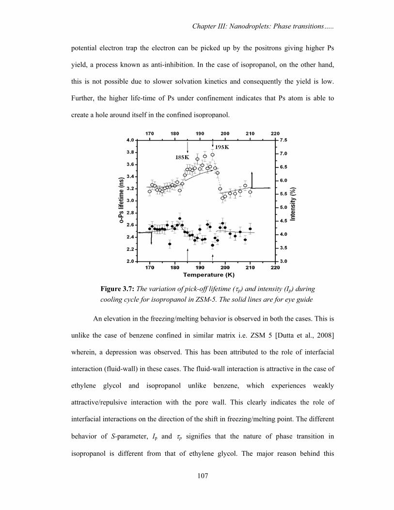
Chapter III: Nanodroplets: Phase transitions…..
107
potential electron trap the electron can be picked up by the positrons giving higher Ps
yield, a process known as anti-inhibition. In the case of isopropanol, on the other hand,
this is not possible due to slower solvation kinetics and consequently the yield is low.
Further, the higher life-time of Ps under confinement indicates that Ps atom is able to
create a hole around itself in the confined isopropanol.
An elevation in the freezing/melting behavior is observed in both the cases. This is
unlike the case of benzene confined in similar matrix i.e. ZSM 5 [Dutta et al., 2008]
wherein, a depression was observed. This has been attributed to the role of interfacial
interaction (fluid-wall) in these cases. The fluid-wall interaction is attractive in the case of
ethylene glycol and isopropanol unlike benzene, which experiences weakly
attractive/repulsive interaction with the pore wall. This clearly indicates the role of
interfacial interactions on the direction of the shift in freezing/melting point. The different
behavior of S-parameter, Ip and τp signifies that the nature of phase transition in
isopropanol is different from that of ethylene glycol. The major reason behind this
Figure 3.7: The variation of pick-off lifetime (τp) and intensity (Ip) during cooling cycle for isopropanol in ZSM-5. The solid lines are for eye guide

Chapter III: Nanodroplets: Phase transitions…..
108
dissimilarity is the difference in the nature of hydrogen bonding in ethylene glycol and
isopropanol molecules, which makes the interfacial interaction different. It is already
mentioned that ethylene glycol has both inter- and intra-molecular hydrogen bonding,
whereas isopropanol has only inter-molecular hydrogen bonding. Hence, under
confinement, isopropanol experiences more attractive interaction with the pore wall. This
causes the extent of elevation ⎟⎟⎠
⎞⎜⎜⎝
⎛ Δ
freezingTT in phase transition temperature higher in the case
of isopropanol. It is observed that the elevation in phase transition temperature in ethylene
glycol is only 3.8%, whereas in isopropanol it is around 7.5% relative to their respective
bulk freezing temperature. Although, the pore size in both the cases remains same, it is
only the distinct interfacial interaction or the surface energy which plays crucial role to
make the phase transition behavior quite different. In isopropanol, since the molecules
strongly interact with the pore surface, the mobility of the molecules near the pore surface
decreases very fast with the decrease in temperature. This may also be one of the reasons
for the different behavior of S-parameter, τp and Ip across the phase transition temperature
in the two cases.
3.3.1b. NMR results
Figures 3.8 shows the variation of spin-spin relaxation times originating from the
protons of the molecules confined primarily in the nanopores. A typical decay curves for
ethylene glycol in ZSM 5 taken at 267 and 240 K, respectively is shown in Figure 3.8. In
the temperature range 230-300 K, T2 decay is expressed as a sum of at least two distinct
components exhibiting Gaussian decay. As a typical example, the deconvolution into two
components (I(1) & I(2)) for 267 K decay curve is shown in the inset of Figure 3.8. The
temperature dependence of the fractional intensities of the two components and their
characteristic times are shown in Figures 3.9 and 3.10, respectively.

Chapter III: Nanodroplets: Phase transitions…..
109
The characteristic time (T2(1)) for I(1) component is in the range of 5 ms and that
of I(2) component (T2(2)) is around 30 ms, showing a decreasing trend with the decrease
in temperature. The obtained time scales indicate that both the components are in the fluid
state, but with different physical environment. The shorter component T2(1) (Figure 3.10)
is ascribed to fluid molecules close to the pore wall. The molecules away from the pore
walls would exhibit relatively longer T2(2) because of the higher mobility like the bulk
fluid. T2(1) is almost temperature independent, however, gradual decrement in T2(2) is
ascribed to slowing down of the molecular motion due to lowering of temperature. The
two components are present at about equal intensities at room temperature and down to
about 270 K. Below this temperature, I(1) begins to increase at the expense of other
component, indicating a transition from a higher to a lower mobility state (similar
discontinuity in the S-parameter is seen at this temperature). This means that fluid pore
wall surface interaction starts to percolate towards the centre of the pore facilitating the
gradual increase in the number of molecules interacting with pore wall. This process
1 10
0
2
4
1 10
0
1
2
3
I(TA
U)
I(TA
U)
Ethylene Glycol in ZSM5
Tau (ms)
Tau (ms)
240 K Theory 267 K Theory
T= 267 K I(1)= 1.55 T2(1)= 9.0 ms I(2)= 1.35 T2(2)= 40 ms
Figure 3.8: Decay of NMR signal intensity for 1H spin-spin relaxation in ethylene glycol in ZSM-5 at 267 and 240 K. Inset: two distinct fractional intensities (I(1) and I(2)) of spin-spin relaxation time (T2) are shown at 267 K.

Chapter III: Nanodroplets: Phase transitions…..
110
Figure 3.10: 1H spin-spin relaxation time (T2) at various temperatures of the molecular components with two different mobilities in ethylene glycol in ZSM-5.
220 230 240 250 260 270 280 290 3000
5
10
15
20
25
30
35
40
45
50
T2(2)
T2(1)
T 2 (m
s)
Temperature (K)
continues down to 260 K (bulk freezing point of ethylene glycol). From 260 K, the
intensity of the component with shorter T2 (I(1) component) starts to dominate and finally
around 235 K, I(2) component i.e. that with longer T2 reduces to 10% of the total
intensity of the resonance line.
Figure 3.9: Temperature variation of fractional intensities of the molecular components having two different mobilities observed in 1H NMR of ethylene glycol in ZSM-5.
220 230 240 250 260 270 280 290 3000.0
0.2
0.4
0.6
0.8
1.0
I(2)
I(1)
I(1),
I(2)
Temperature (K)

Chapter III: Nanodroplets: Phase transitions…..
111
Shorter T2 component as explained before indicates the presence of strong surface
bonded molecules. The other component having longer T2 shows the existence of
molecules free to move, but still close enough to the surface so that the surface interaction
becomes dominant at about 10 degrees above the bulk freezing point, when the molecular
motion is slowed down. It may be said that the part of adsorbed ethylene glycol that
exhibits fluidity at room temperature, experiences a gradual decrease in mobility below
270 K. Probably, the high degree of compartmentalization prevents the occurrence of a
long range crystalline order at a sharply defined temperature as it happens in a bulk fluid.
A possible reason for this could be the pore size in the present case (0.5-1.3 nm), which is
comparable to the molecular size, and much smaller compared to other porous materials
with a larger pore size (6 - 50 nm) where definite signature of the crystalline state has
been observed upon freezing [Gussoni et al., 2004].
In the case of isopropanol, T2 decay in the temperature range 295-200 K, could be
satisfactorily expressed as a sum of three components exhibiting Lorentzian decay. Figure
3.11 shows a typical example of one such fitting at 220 K. The temperature dependence
Figure 3.11: Decay of NMR signal intensity for 1H spin-spin relaxationin isopropanol at 220 K.
0.01 0.1 1 100.0
0.5
1.0
1.5
2.0
2.5
3.0
3.5 T= 220 K I(1)= 2.2 T2(1)= 0.07 ms I(2)= 0.85 T2(2)= 1.1 ms I(3)= 0.7 T2(3)= 7.0 ms I=I(1)+I(2)+I(3)
I(TA
U)
TAU (ms)

Chapter III: Nanodroplets: Phase transitions…..
112
of the fitting parameters, I(i) and T2(i) is shown in Figures 3.12 and 3.13. The values of
T2, which are about 0.07 ms, 1.0 ms, and 5.0 ms, do not show appreciable change with
temperature. The component having the shortest T2 (0.07 ms) remains dominant, at about
70 %, throughout the temperature range. This component indicates the presence of
isopropanol molecules rigidly bonded inside the pores via strong surface interaction. The
component having such a small value of T2 has not been seen in ethylene glycol,
signifying weaker interaction of ethylene glycol with the pore surface. The intermediate
and long components of T2 in isopropanol signify the presence of molecules having
relatively higher mobility. Below about 200 K, the component with the longest T2 is
gradually diminished, and no longer obtained below 190 K, which is indicative of gradual
freezing of molecular mobility, or a phase transition of molecules away from the pore
surface.
Figure 3.12: Temperature variation in fractional intensities of the molecular components with three different mobilities observed in 1H NMR of isopropanol in ZSM-5.
180 200 220 240 260 280 300
0.0
0.1
0.2
0.3
0.4
0.5
0.6
0.7
0.8
I(3)
I(2)
I(1)
I(1),
I(2),
I(3)
Temperature (K)

Chapter III: Nanodroplets: Phase transitions…..
113
3.3.1c. Discussion
PAS and NMR measurements in ethylene glycol and isopropanol thus, explored the
nature of the phase transition of two liquids having different liquid-substrate interfacial
interaction within the confinement. The structures of the quasi-solid state of ethylene
glycol and isopropanol near or below their bulk freezing temperatures depend on the
relative strength of the interaction within the molecules as well as between the molecules
and the pore wall. The oxygen atoms present on the surface of the void space of ZSM 5
enhances the effect of the interfacial hydrogen bonding, which provides a strong spatial
correlation and supports the propagation of surface induced order to the molecules at the
centre of the pore. The fluid molecules having strong interaction with the surface of the
pore are generally arranged in a layer structure [Morineau, et al., 2003; Abragam et al.,
1961]. Hence, the present situation facilitates the layer like configuration of strongly
hydrogen bonded molecules like isopropanol. The ethylene glycol, on the other hand,
which shows comparatively weaker interfacial hydrogen bonding due to presence of
strong intra-molecular hydrogen bonding, is expected to have inhomogeneous phases
Figure 3.13: 1H spin-spin relaxation time (T2) at various temperatures of the molecular components with three different mobilities in isopropanol in ZSM-5.
180 200 220 240 260 280 300
0
1
2
3
4
5
6
7
8
T2(3)
T2(2)
T2(1)
T 2 (m
s)
Temperature (K)

Chapter III: Nanodroplets: Phase transitions…..
114
with globular structure as observed in case of benzene in silica pores by Dutta et al.
[Dutta et al., 2008]. An inhomogeneous phase with partial crystalline domain is also
reported by Radhakrishnan et al. and Bartkowiak et al. using Monte Carlo simulation
method in the context of freezing of nitrobenzene in silica [Radhakrishnan et al., 2000;
Bartkowiak et al., 2001].

Chapter III: Nanodroplets: Phase transitions…..
115
II. Phase transitions of water confined in clay
nanopores

Chapter III: Nanodroplets: Phase transitions…..
116
3.3.2. Water confined in saponite clay
3.3.2a. TG-EGA results
The presence of water in the clay sample was confirmed and the amount was
determined by monitoring the evolved water from the samples using simultaneous TG-
EGA measurements. Figure 3.14a shows the mass (%) change in the clay samples as a
function of temperature while the inset shows the extracted IR spectrum of the
corresponding evolved gas at 423 K. The as-synthesized saponite clay shows 22% mass
loss whereas the sample heated at 493 K for 15 hrs shows no mass loss in the temperature
range 298-500 K (Figure 3.14a). This indicates that as-synthesized clay (hydrated)
contains 22% water whereas no water is present in the heated sample (dry clay). The inset
FTIR spectrum of the evolved gas confirms the presence of water in the as-synthesized
clay sample through 1506 and 3600 cm-1 IR bands corresponding to H−O−H bending and
stretching vibrations, respectively. Hence, the respective mass loss corresponds to the
amount of water present in the clay sample. The desorption temperature (Tdesorb), is the
maximum obtained by differentiating the mass-temperature curve with respect to
temperature, defines the maximum rate of desorption of liquid from the sample. The
differentiated mass-temperature (DW) profile can be used to identify different adsorption
sites for the liquid inside the matrix [Yudasaka et al., 2005]. In the present case, DW
profile is seen to be asymmetric as shown in Figure 3.14b and the desorption behavior of
water is obtained by deconvoluting DW profile. DW profile has been deconvoluted into
two peaks (Figure 3.14b) which indicate two adsorption sites or two regimes of water
(distinctly bonded water molecules confined within the clay nanopores).
We have analyzed the manner in which 22% water is distributed in the clay
nanopores. The diameter of a water molecule is 0.275 nm and external surface area of

Chapter III: Nanodroplets: Phase transitions…..
117
saponite used is 315 m2/g. A dense monolayer close to the wall surface requires 7 mM of
water per gram of saponite.
Figure 3.14a: Mass (%) loss as a function of temperature (mass-temperature curve) for dry and hydrated clay as measured from TG-EGA. Inset shows FTIR spectrum of the evolved gas.
Figure 3.14b: DW profile for hydrated clay as obtained from mass-temperature curve.

Chapter III: Nanodroplets: Phase transitions…..
118
For 22% water confined in the pores, the amount of water is 12 mM per gram of
saponite, which is about twice the amount required for the densely packed monolayer.
This shows that 22% water in saponite would form two water layers on the surface of the
platelets. The interplatelet spacing of 15.4 Å as obtained from XRD measurement in as-
synthesized clay includes thickness of rigid clay platelets and interplatelet distance.
Considering the interplatelet spacing of clay, not more than two layers can be
accommodated between the platelets. Neutron scattering studies in vermiculite clay by
Skipper [Skipper et al., 1991] has shown that water in interplatelet spaces is associated
with the platelet surface and interplatelet cations forming hydration layer around the
cations. Each water molecule in the coordination sphere directs one of its hydrogen atoms
towards the platelet to form hydrogen-bond with the surface oxygen atom. However, the
exact position of cations within the platelets could not be deduced from these experiments
and there is no reason to assume that cations would lie only midway between the clay
platelets. Therefore, it can be assumed that out of the total water molecules, few
molecules are attached to the cations as well as the platelet surface. These water
molecules are more bound as compared to the relatively free water molecules which do
not form hydrogen-bond with the platelet surface but can be hydrogen-bonded to other
water molecules in the close vicinity.
3.3.2b. ATR-FTIR results
Figure 3.15 shows ATR-FTIR spectra of hydrated and dry clay. The spectra show
different vibrational modes of water confined in clay nanopores in the hydrated sample.
The vibrational modes observed at 1641 and 3000-3600 cm-1 correspond to OH-bending
and OH-stretching (OHS) modes of water, respectively. The band at 970 cm-1 is attributed
to the combination of OH-libration (686 cm-1) and OHS (3000-3600 cm-1) bands of water.
The vibrational mode involving stretching motion of the intramolecular OH-bond is

Chapter III: Nanodroplets: Phase transitions…..
119
sensitive to the strength of the hydrogen-bonding between the water molecules. Within a
sample, especially in confined geometries, there may exist a variety of molecules that are
differently coordinated to each other. With this in mind, we have deconvoluted OHS
spectrum into four Gaussian components (as shown in the inset of Figure 3.15) viz. (a)
3110 cm-1, (b) 3230 cm-1, (c) 3425 cm-1 and (d) 3600 cm-1, coming from well established
studies of OHS vibrational spectrum of water [Brubach et al., 2005; Mallamace et al.,
2007]. The low frequency contributions 3110 and 3230 cm-1 are attributed to hydrogen-
bonded water molecules. The component at 3110 cm-1 confirms the presence of confined
water in the form of tetrahedrally coordinated water clusters and 3230 cm-1 corresponds to
symmetric OH vibrations observed in liquid water [Mallamace et al., 2007; Kittaka et al.,
2009]. The components at higher frequencies 3425 cm-1 and 3600 cm-1 correspond to less
hydrogen-bonded molecules. These frequencies are close to that of water molecules
existing in the form of dimer or multimer water, respectively.
Figure 3.15: ATR-FTIR spectra of dry and hydrated clay. Inset shows the deconvoluted OHS band of water (3000-3600 cm-1). OHS band is deconvoluted into four peaks (a, b, c and d).

Chapter III: Nanodroplets: Phase transitions…..
120
3.3.2c. DSC results
Figure 3.16 shows the conventional DSC curves for hydrated and dry clay in the
temperature range 200-298 K in the cooling and heating scans. In the hydrated clay, a
peak at T~ 230 K is observed during the cooling scan which becomes broader and shifts
to higher temperature during the heating scan. No transition peak is observed in dry clay
throughout the temperature range. Therefore, the peak observed in hydrated clay at T~
230 K is attributed to the freezing/melting or a similar phase transition of the confined
water. The broad nature of the peak does not allow us to determine the onset of transition
temperature and indicates that the phase transition spreads over a wide temperature range.
The presence of low temperature peak has been observed for water confined in variety of
porous media [Kozlowsk et al., 2012; Schreiber et al., 2001; Tombari et al., 2005] and
attributed to the depression in the freezing/melting behavior of water. The apparent
specific heat capacity Cp for water confined in clays calculated by Kozlowski et al. using
modulated DSC indicated the presence of partial freezing/inhomogeneous phases
[Kozlowsk et al., 2012]. However, different thermal characteristics have been observed in
different materials. In the present study, the observed low temperature peak may be
attributed to a low-temperature phase transition involving partial freezing of the confined
water.
The Cp of confined water is calculated by subtracting Cp of dry clay from the Cp of
hydrated clay as measured in temperature modulated mode and is shown in the inset of
Figure 3.16. The Cp of confined water is seen to be lower than the bulk water (4.18 Jg-1K-
1). This could be a manifestation of the effect of confinement as also suggested by
Kozlowski [Kozlowsk et al., 2012]. It is also observed that the obtained Cp increases with
the decrease in temperature and shows a maximum at ~230 K corresponding to the low-
temperature phase transition of confined water. The increase in Cp is an indicative of more

Chapter III: Nanodroplets: Phase transitions…..
121
configurational contribution to heat capacity than the contribution from vibrational and
anharmonic modes. Changes in the average coordination and short range order in the
structure of liquid contribute to the configurational part of heat capacity. Therefore, the
variation of Cp as a function of temperature reveals structural changes in confined water
whereas, the low-temperature peak can be assigned to the partial freezing of confined
water molecules.
3.3.2d. PAS results
Positron lifetime measurements have been carried out at room temperature for
hydrated and dry clay samples. The lifetime spectrum for the hydrated clay could be
decomposed into three life-time components; however, four components were obtained
for the dry clay. The measured life-times and intensities are shown in Table 3.1. The
presence of only one Ps like state (long component) in a system with confined fluids as
compared to two distinct Ps like states in the absence of confining fluid has been
Figure 3.16: Heat flow per unit mass in dry and hydrated clay in cooling and heating scans. The inset shows the apparent heat capacity (Cp) of confine water obtained by subtracting Cp of dry clay from the hydrated clay.

Chapter III: Nanodroplets: Phase transitions…..
122
observed by others too [Kajcsos et al., 2000; Dutta et al. 2006]. In the context of present
work, the observed result reveal localization of positron/Ps in nanoconfined water in clay.
Sample τ1
[ns] I1
[%] τ2
[ns] I2
[%] τ3
[ns] I3
[%] τ4
[ns] I4
[%]
Hydrated clay
0.226
(± 0.009)
38.42
0.490
(± 0.017)
43.63
2.115
(± 0.024)
17.94
-----
-----
Dry Clay
0.200 (±0.016 )
28.06
0.439
(± 0.015)
54.5
1.86
(± 0.066)
10.12
10.75
(± 0.200)
7.3
Figures 3.17 and 3.18 show the variation of S-parameter as a function of
temperature for dry and hydrated clay, respectively. The S-parameter profile for dry clay
(Figure 3.17) shows insignificant variation unlike the hydrated clay (Figure 3.18) which
shows distinct features over the studied temperature range in cooling as well as heating
cycle. The change of slope/discontinuity in S-parameter profile as a function of
temperature is indicative of phase transition of liquid confined in nanodomains [Dutta et
al., 2006 & 2008]. In the present context, the absence of variations in S-parameter profile
in the dry clay shows that the features seen in the hydrated clay are signatures of phase
transition of water confined in clay nanopores. Two phase transitions have been observed
for the confined water viz. above (high-temperature transition, HTT) and below (low-
temperature transition, LTT) the bulk freezing temperature (Figure 3.18) of water (273
K). The HTT and LTT range from 286-274 K and 254-240 K, respectively. Figure 3.18
also shows S-parameter profile for the heating cycle showing the presence of both the
transitions in addition to a marked hysteresis for HTT. The hysteresis behavior of
confined liquids has been observed by others and is explained on the basis of
thermodynamical stability of the phases taking into account surface energy barriers
Table 3.1: Positron lifetime and intensities at room temperature for the hydrated and dry clay sample

Chapter III: Nanodroplets: Phase transitions…..
123
Figure 3.18: Variation of S-parameter with temperature for hydrated clay in cooling (○) and heating (●) cycle.
[Morishige et al., 1999]. The origin of hysteresis observed in the present study could be
the inhomogeneities brought out by the strong surface interactions as well as the effect of
confining geometry [Brun et al., 1977; Vanfleet et al., 1995; Gross et al., 1997].
The variation of o-Ps pick-off life-time (τ3) and intensity (Ip) as a function of
temperature for hydrated clay are shown in Figure 3.19. It is seen that τ3 increases to a
maximum value (around T~268 K) after the completion of HTT, and, the corresponding
Figure 3.17: Variation of S-parameter with temperature for dry clay.

Chapter III: Nanodroplets: Phase transitions…..
124
intensity Ip decreases significantly followed by a marginal increase that remains nearly
constant upto the lowest temperature studied. No significant change in τ3 and Ip are seen at
LTT unlike S-parameter. However, it is interesting to note that Ip remains constant around
11% till the lowest temperature studied. Figure 3.20 shows the change in free volume (fv
= (4π/3)*r3) with temperature, where r is the radius of the free volumes as calculated
from τ3 using Tao-Eldrup equation [Tao, 1972 and Eldrup et al., 1981],
(3.12)
where, Δr is the empirical electron layer thickness (0.166 nm). The significant variation
of fv suggests nanostructural alterations with temperature.
1
31 1 21 sin2 2
r rr r r r
πτπ
−⎛ ⎞⎛ ⎞= × − + ⎜ ⎟⎜ ⎟+Δ +Δ⎝ ⎠⎝ ⎠
Figure 3.19: Variation of o-Ps pick-off lifetime (τ3) and intensity (Ip) as a function of temperature.

Chapter III: Nanodroplets: Phase transitions…..
125
The presence of two phase transitions, above and below the bulk freezing point of
water, is the first report on the phase behavior of nanoconfined water. Phase transition
below the bulk freezing temperature of water has been observed by many authors for
water confined in different geometries and assigned to supercooled water [Bruni et al.,
2011; Mallamace et al., 2006]. However, the transition seen at elevated temperature
(HTT) in the present study is observed for the first time for water confined in clay
nanopores. The shift in freezing/melting behavior has been explained on the basis of
nature of fluid-wall interaction [Miyahara et al., 1997; Radhakrishnan et al., 2002]. It has
been shown that the attractive interaction with the wall surface results in the elevation of
the freezing point, whereas, depression is observed in the case of repulsive (less
attractive) interaction. On this basis, we feel that the observed HTT (above bulk freezing
point), represents phase transition associated with the water molecules hydrogen-bonded
to cations as well as platelets surface (bound water). However, the concurrent presence of
a transition below the bulk freezing point (LTT) of water evidently reveals existence of
different regimes of confined water. In order to get further insight into these transitions
both NMR and DRS studies have been carried out as detailed in the latter section.
Figure 3.20: Variation of free volume (fv) with temperature. Error bar lies within the symbols.

Chapter III: Nanodroplets: Phase transitions…..
126
It is seen that the positron annihilation parameters viz. S-parameter, τ3 and Ip are
sensitive to phase transitions in confined systems and explore nanostructural alterations
following the transitions. The studies on phase transition of confined liquids have always
shown anomalous changes in S-parameter, τ3 and Ip near the transition. The onset of
transition is marked by a decrease in S-parameter similar to the present observation. The
completion is associated with the minimum in S-parameter which increases on further
cooling to a value similar to that at the onset of transition. This is explained on the basis
of structural inhomogeneities existing in the confined systems which include the presence
of inhomogeneous phases due to partial freezing, agglomeration or clustering of
molecules and the appearance of more surfaces and interfaces due to freezing [Dutta et
al., 2006 & 2008]. In addition, positron/Ps dynamics in the confined system viz.
trapping/detrapping and annihilation from delocalized states are also invoked to explain
the S-parameter and τ3 behavior.
While the two observed transitions are associated with significant change in
electron momentum distribution as reflected in S-parameter, it is interesting to note the
variation in free volume, fv. It significantly increases below HTT, reaches a maximum
(~268 K) and decreases till the lowest temperature studied. The variation of S-parameter
and fv at HTT suggest rearrangement of water molecules leading to structural ordering of
molecules near the surface. This ordering results into a new phase (configuration) with
large open/free volumes. On the other hand, at LTT, the variation in fv is not as
pronounced as S-parameter. Electron momentum distribution seems to be a more sensitive
index as compared to electron density associated with this transition. Although the exact
reason for this behavior is not known, a possible reason could be the fact that S-parameter
provides a composite information on p-Ps, free positron and o-Ps states unlike o-Ps life-
time (free-volume size). An empirical viscosity-free volume correlation i.e. η = A exp

Chapter III: Nanodroplets: Phase transitions…..
127
(1/fv) suggested by Miller indicates an inverse relation between fv and η [Miller et al.,
1963]. Therefore, the observed variation in fv (monotonic decrease) indicates increase in
the viscosity of water as temperature is lowered. This behavior corresponds to
supercooled liquids which become increasingly viscous as temperature approaches glass
transition, Tg (Tg of water is lower than the lowest temperature studied in the present
case). It is also to be noted that IP reduces to 11% below HTT and remains nearly same
till the lowest temperature studied (even below LTT). This indicates that confined water
does not completely freeze to crystalline ice at LTT. On the basis of these observations,
we conjecture that the LTT is associated with the supercooled water molecules.
3.3.2e. NMR results
NMR measurements have been performed in static and MAS mode for hydrated
clay sample. A single broad peak observed in static case is resolved into two distinct
peaks in MAS case coming from the confined water molecules (around 4 ppm) and Si–
OH groups (around 0 ppm) as shown in Figure 3.21. The confined nature of water trapped
inside the clay nanopores is the reason behind the extremely broad NMR peak of water
observed in static case. Anisotropic interactions like chemical-shift anisotropy and
dipolar-dipolar interactions are strong under these conditions. Partial averaging of these
interactions by MAS leads to narrower NMR peak of water.
Isotropic chemical-shifts, δ, of nuclei like protons reflect the kind of electronic
environment experienced by them in a system. Any changes in the local electronic
environment of these nuclei will be accompanied by chemical-shift changes. Water
molecules form an extensive hydrogen-bonding network with each other. It has been
generally observed that the strength of this network weakens (lengthening of hydrogen-
bonds) with increase in temperature [Yamaguchi et al., 2001]. This change has a direct
influence on the 1H chemical-shifts of the water molecules, which for example, can

Chapter III: Nanodroplets: Phase transitions…..
128
Figure 3.21: 1H chemical shift (δ) of water as a function of temperature when the clay sample is spinning at 5 kHz at magic angle inside NMR spectrometer. Temperature dependence data from 245-280 K and 290-325 K is fitted to two independent straight lines, yielding temperature coefficient (g) values of -12.08 and -4.35 ppb K-1.
change by -11.9 ppb K-1 in the case of bulk water [Wishart et al., 1995]. One can thus
obtain information about the kind of structural environment experienced by a water
molecule by monitoring δ as a function of temperature. Thus, a careful examination of δ
as a function of temperature can provide details of the thermal evolution of water
configurations in terms of local hydrogen-bonded geometry, especially in supercooled
regime. 1H δ obtained from MAS spectra of water trapped inside clay nanopores, plotted
as a function of temperature, is shown in Figure 3.21. The temperature dependence of δ
(temperature coefficient, g) could not be fitted to a single straight line in this case. Water
molecules yield different values of g viz. -12.08±0.4 and -4.35±0.1 ppb K-1 when
temperature is varied from 245 to 280 and 290 to 325 K, respectively. It is seen that the
chemical-shift between 280 and 290 K could not be fitted to either of the straight lines.
This indicates that the water molecules trapped inside the clay nanopores undergo
significant changes in their hydrogen-bonding network when the temperature is lowered

Chapter III: Nanodroplets: Phase transitions…..
129
from 290 to 280 K. Moreover, g values in these two regimes reveal that the trapped water
resembles bulk-like water (in terms of hydrogen-bonding network) at lower temperatures
(T < 280 K), while it exists as a less mobile liquid at higher temperatures (T > 290 K) as
indicated by high g value of -4.35 ppb K-1. This region corresponds to the HTT, observed
in positron annihilation studies.
Figure 3.22: Transverse relaxation times (T2
* and T2′) of water as a function of temperature when clay sample is (a) static and (b) spinning at 5 kHz at magic angle inside NMR spectrometer. Dotted lines in both the plots indicate inflection points in the measured T2′ values as a function of temperature.

Chapter III: Nanodroplets: Phase transitions…..
130
Figure 3.22 shows the variation of T2* and T2′ values with temperature in static
(Figure 11a) and MAS (Figure 11b) modes. All the curves show two inflection points,
near 290 and 260 K. These inflection points are seen to be more pronounced in the case of
T2′ values obtained from the static mode. The variation of T2* and T2′ at 290 and 260 K
are indicative of change in dynamical properties of water and can be associated with the
phase transition of confined water. The transition at 290 K can be associated with the
change in local hydrogen-bonding network of water molecules as indicated by the change
in the value of temperature coefficient of 1H chemical-shift which leads to a structural
rearrangement of water molecules resulting in a network having bulk-like configuration.
We now correlate the changes observed in the structural and dynamical properties
of water confined in the clay nanopores as indicated by temperature coefficients (g) and
transverse relaxation times (T2* and T2′), respectively. At higher temperatures (T > 290
K), water exists as a less mobile liquid, with each molecule experiencing a strong
hydrogen-bonding network (g = -4.35 ppb K-1). The lowering of temperature in this
region decreases the mobility of water molecules and, as a result, transverse relaxation
times are shortened. The slow rise of transverse relaxation times when the temperature is
lowered from 290 to 260 K can be explained on the basis of partial
freezing/immobilization of water molecules resulting into two different regimes of
molecules whose relaxation times differ significantly.
The water molecules close to the platelet surface (hydrogen-bonded to the surface
as well as cations) get immobilized due to relatively attractive interaction with the surface
as compared to the molecules away from the surface. The relaxation time of these
immobile molecules falls off rapidly as compared to other molecules. The water
molecules which are away from the surface (relatively less bound) have mobility akin to
molecules present in bulk water as indicated by g value (-12.1 ppb K-1) and hence, yield

Chapter III: Nanodroplets: Phase transitions…..
131
much longer relaxation times. This scenario can be well understood from Figure 3.23,
wherein, eye guide (solid and dashed) indicate two regimes I and II of water molecules
representing faster relaxation of water molecules near the platelet surface and slower
relaxation due to the molecules away from the platelet surface, respectively. The resultant
of two relaxation processes results in the slow rise of T2′(T2*) from 290 to 260 K. As the
temperature is lowered further, the overall relaxation time is dominated more and more by
the water molecules in the regime II (bulk-like phase). Below 260 K, decrease in
transverse relaxation time indicates decrease in the mobility of water due to the decrease
in temperature.
3.3.2f. DRS results
Figure 3.24a and 3.24b show the three-dimensional plots of frequency (f) and
temperature dependence of the measured dielectric loss i.e. imaginary part of permittivity
(ε″(f)) in hydrated and dry clay, respectively. The dielectric response of the two samples
are significantly different throughout the studied temperature range.
Figure 3.23: Transverse relaxation time (T2′) of water as a function of temperature obtained in the static mode. Solid and dashed lines (eye guides) represent the likely scenario of the freezing phenomenon of water layers.

Chapter III: Nanodroplets: Phase transitions…..
132
Figure 3.25 shows the dielectric response at T = 278 K for both the samples,
which indicates different relaxation processes in the two cases. The strong loss peak near
106 Hz is present in both the samples and does not show any temperature dependence.
This peak is also present in the dielectric response of empty cell with the Teflon spacer,
Figure 3.24: Three dimensional representation of temperature and frequency dependence of imaginary part of the dielectric permittivity (ε′′(f)) or dielectric loss for (a) hydrated and (b) dry clay.

Chapter III: Nanodroplets: Phase transitions…..
133
and we, therefore, attribute it to the empty cell with spacer. In addition to high frequency
loss peak (106 Hz), two more relaxation processes are seen in the dielectric response of
hydrated clay. The large loss peak (main relaxation process) shows strong temperature
dependence whereas, the weak peak (secondary relaxation process) is seen to be
swamped by the presence of the main relaxation process above 210 K and hence, could
not be discerned from the dielectric response in the temperature range 300-220 K (Figure
3.24). Therefore, the present study mainly concentrates on the main relaxation process.
The peak due to main relaxation process observed in hydrated clay is clearly absent in the
dry clay. This suggests that the main relaxation process arises from the water molecules
confined in the clay. This peak shifts to higher frequencies with the increase in
temperature (Figure 3.24a), and at 278 K it is located at about 104 Hz (Figure 3.25). The
dipolar rotation of liquid water molecules is a fast process, of the order of 10-12 seconds
and this time scale lies beyond the limits of detection of our instrument. Thus, the
processes responsible for the main relaxation peak are most likely a combination of
interfacial polarization involving water molecules and conductivity effects. The low
Figure 3.25: Dielectric response of hydrated and dry clay at T = 278 K.

Chapter III: Nanodroplets: Phase transitions…..
134
Figure 3.26: Dielectric response ((ε′′(f)) vs. f) for hydrated clay at 250 K. The solid line represents the fit to the response using sum of power law and HN function; dotted and dash-dot curves represent the main relaxation process and d.c. conductivity contribution, respectively.
frequency dispersion is observed in both the samples and is ascribed to conductivity
contribution from the sample. It may also be noted that the weak loss feature at lower
temperatures in dry clay is qualitatively different from that observed in hydrated clay, and
must therefore, have a different origin. Further analysis of the main relaxation process to
obtain relaxation times has been carried out by fitting the dielectric response curves (ε″(f)
vs. f ) with the sum of a power law (d.c. conductivity) and a well known Havriliak-
Negami (HN) function,
( )( )[ ] ⎥
⎥⎦
⎤
⎢⎢⎣
⎡
+
Δ+= −
βαωτ
εωεσ
ωεi
n
o
DC
1Im"
(3.13)
where, ω = 2πf, Δε = εS-ε∞, where, εS and ε∞ are static and high frequency limiting values
of the dielectric constant, respectively, εo is the permittivity of free space, σDC is the
conductivity contribution, τ is the relaxation time and n, α and β are empirical exponents
with values between 0 and 1. As an example of this fitting, the dielectric loss spectrum of
the hydrated clay at 250 K is shown in Figure 3.26.

Chapter III: Nanodroplets: Phase transitions…..
135
The main relaxation process is the only dominant relaxation observable at this
temperature and is shown with a dotted curve along with the conductivity contribution.
For the spectra at temperatures below 210 K, two HN functions are required to fit the
dielectric response. However, due to small amplitude of second relaxation process at low
temperatures (below T=210 K) it could not be discerned from the response curve.
In the case of dry clay, the only relaxation process apart from the low frequency
dispersion shows weak loss in the temperature range 298-210 K. This process is seen to
be different from that observed in hydrated clay, and shows Arrhenius temperature
dependence of relaxation time over the studied temperature range. The activation energy
of this process is found to be EA ≈ 0.72 eV, which is higher than that for the process
observed in hydrated clay (Table 3.2, discussed below). The origin of this process is not
clear but this feature is not observed in hydrated clay where it might have been swamped
by low frequency dispersion.
The relaxation time τ corresponding to the main relaxation process in hydrated
clay shows strong temperature dependence over the range 298-210 K. The plot of
temperature dependence of τ is given in Figure 3.27. It is interesting to note that the
relaxation time, τ follows Arrhenius behavior at temperatures below 240 K and a non-
Arrhenius behavior above 240 K. In fact, above 240 K, the behavior could be very well
approximated by a Vogel-Fulcher law (see below). The temperature dependence of τ for
the main relaxation process are fitted as,
( ) ⎟⎟⎠
⎞⎜⎜⎝
⎛=
TkE
TB
ao expττ
for T ≤ 240 K (3.14)
( ) ( )⎟⎟⎠
⎞⎜⎜⎝
⎛−
=o
oo TT
BTT expττ
for T ≥ 240 K (3.15)

Chapter III: Nanodroplets: Phase transitions…..
136
Figure 3.27: Temperature dependence of relaxation time (τ) for the main relaxation process in hydrated clay, fitted to Arrhenius (210-235 K) and Vogel-Fulcher (240-300 K) functions.
where, Ea is activation energy, kB is Boltzmann constant, T is the temperature, B is a
dimensional normalization factor, τ0 is a pre-exponential factor and To is Vogel-Fulcher
(VF) temperature. The best fit values for the Arrhenius and VF behavior are tabulated in
Table 3.2.
Arrhenius Fit Vogel-Fulcher Fit
Parameter Value Parameter Value
Ea 0.257 eV E 0.027 eV
τ0 7.17x10⁻⁹ s τVF 5.34x10⁻⁷ s
----- ---- TVF 200 K
The variation of relaxation time with temperature shows that the dynamics of
water confined in clay nanopores shows a cross over from non-Arrhenius to Arrhenius
Table 3.2: Fitting parameters for hydrated clay; Arrhenius fit (T< 240 K) and Vogel-Fulcher fit (T> 240 K).

Chapter III: Nanodroplets: Phase transitions…..
137
temperature dependence around 240 K. However, the values of the relaxation times are
much slower than those reported for rotational dynamics of water molecules [Swenson et
al., 2000; Bergman et al., 2000] and hence cannot be attributed to these processes. As
mentioned earlier, this relaxation may be a combination of interfacial polarization and
conductivity effects involving the water molecules. Even so, the cross over from one type
of temperature dependence to another, as observed in Figure 3.27, suggests a transition.
This change in behavior near 240 K matches well with the low-temperature transition
observed in our positron annihilation study. Since conductivity effects are likely to be
dominant in liquid water as compared to frozen water, we may infer that substantial
amount of liquid water exists above 240 K. On this basis, we may conjecture that the
observed cross over at 240 K is related to the partial freezing of supercooled water which
results in the change in conductivity contribution owing to the frozen phase of water.
3.3.2g. Discussion
Two phase transitions viz. above (HTT) and below (LTT) the bulk freezing
temperature of water have been observed for water confined in clay nanopores. PAS is
seen to be sensitive to both the transitions unlike other techniques. While DSC and DRS
are not sensitive to HTT, NMR provides the strongest evidence of structural and
dynamical changes associated with this transition. As discussed earlier, two layers of
water molecules can be accommodated between the clay platelets. These water molecules
exist in two different regimes, molecules hydrogen-bonded to platelet surface as well as
cations are more bound as compared to the molecules away from the surface [Skipper et
al., 1991]. Based on our earlier studies, HTT is expected to be associated with the
molecules experiencing more attractive interactions with the surface of the platelets.
NMR study reveals that HTT is associated with the structural rearrangement of water
molecules as reflected in the variation of 1H chemical-shift with temperature. The change

Chapter III: Nanodroplets: Phase transitions…..
138
of slope of chemical-shift with temperature (g) from -4.35 to -12.08 ppb/K around 284.4
K indicates alteration in hydrogen-bonded network of water molecules. The increase in τ3
and S-parameter below HTT signify structural alterations in terms of increase in free
volume/open space and is consistent with NMR observation. The transverse relaxation
time measured in NMR reveals change in dynamical properties of water molecules at
HTT. The slow rise around 290 K (near HTT) is explained on the basis of different
relaxation times which have arisen due to the existence of different regimes of confined
water (discussed earlier). This has been correlated to the immobilization of water
molecules (faster relaxation) close to the platelet surface (bound molecules) as compared
to the slower relaxation of molecules away from the platelet surface. It is also to be noted
that a marked hysteresis is observed for HTT in PAS owing to thermal stability of the
phases at the surface. On the basis of NMR and PAS results, HTT is expected to be
associated with the phase behavior of water molecules bound to the platelet surface i.e.
immobilization of these water molecules together with the structural rearrangement of
confined water. Below HTT, rest of the water molecules tend to form hydrogen-bonded
network and behave as bulk-like phase as reflected from the variation of 1H chemical-
shift with the decreasing temperature (g = -12.08 ppb/K).
The presence of LTT is observed from PAS, DSC and DRS. This transition can be
related to water molecules forming hydrogen-bonded network similar to bulk water (g = -
12.08 ppb/K). The S-parameter has shown significant change at this transition unlike fv, IP
and 1H chemical-shift. The change in S-parameter can be explained on the basis of
alteration in electron momentum distribution owing to the change in the phase behavior
of water at this temperature. The significant and nearly constant value of IP (~11%) shows
that the confined water does not freeze till the lowest temperature studied. In DSC, a peak
has been observed corresponding to LTT. This low temperature peak has been attributed

Chapter III: Nanodroplets: Phase transitions…..
139
to the depression in freezing/melting point of confined water by many authors. However,
its correspondence to incomplete freezing has been explained by Kozlowski et al. Though
DRS is sensitive to relaxation dynamics of molecules (dipolar relaxation), in the present
case, the measured relaxation time corresponds to the combination of interfacial
polarization and conductivity contribution from the sample. This relaxation process
shows a cross over from non-Arrhenius to Arrhenius behavior around 240 K. The
observed cross over in the behavior of relaxation time can be correlated to change in the
phase behavior which results in the change in conductivity contribution of the sample.
Though no clear evidence for any structural or dynamical change for confined water is
observed at LTT, the results from PAS, DSC and DRS indicate incomplete freezing
and/or depression in freezing /melting point of confined water.
3.4. Conclusions
Phase transitions in nanodroplets (ethylene glycol and isopropanol confined in
ZSM 5 and, water confined in saponite clay) have been studied using different techniques
viz. PAS, NMR and DRS. The structural and dynamical properties were indexed to probe
the phase transitions. The effect of fluid-surface interfacial interaction on the
freezing/melting point of confined ethylene glycol and isopropanol was examined. An
elevation in the freezing/melting point was seen and attributed to the attractive interaction
between the liquids and wall of the confining geometry (ZSM 5). However, the strength
of the (attractive) interaction has significant influence on the extent of the shift, as clearly
seen from different degree of shifts in the two cases. The strong interaction in the case of
isopropanol owing to inter-molecular hydrogen bonding resulted in higher degree of shift
in contrast to ethylene glycol where, due to both inter- and intra molecular hydrogen
bonding the effective interaction with the surface is weaker.

Chapter III: Nanodroplets: Phase transitions…..
140
The phase behavior of nanoconfined water in slit like pores of saponite was
studied. The effect of strong hydrogen bonding between water molecules as well as water
molecules and the surface of platelet strongly influence the structural and dynamical
properties of confined water. Two phase transitions viz. above (HTT) and below (LTT)
the bulk freezing temperature of water were observed and attributed to different regimes
of confined water (role of interfacial interactions). The presence of HTT is the first report
on the phase behavior of nanoconfined water. The structural and dynamical parameters
suggest that HTT involves structural modification in terms of hydrogen-bonded network
and dynamic arrest/immobilization of water molecules close to the platelet surface owing
to attractive interaction with the surface. On the other hand, LTT is conjectured to be
associated with the partial freezing of confined water as evident from PAS, DRS and
DSC. The present study mainly highlights the effect of role of interfacial interaction on
the phase transition of confined liquids.

Chapter IV: Pore architecture of…..
141
CHAPTER-IV
Pore architecture of membranes

Chapter IV: Pore architecture of…..
142
Membranes based processes are an active area of interest for scientific community
engaged in developing new membranes and understanding the microscopic aspects of
their transport mechanism. Membrane processes are broadly divided on the basis of the
intrinsic pore sizes in liquid as well as gas permeation based separation schemes. For
example, reverse osmosis, pervaporation as well as gas separation schemes have pore
sizes below 0.8 nm while nanofiltration of liquid or gas separation using ceramic
membranes have pore sizes in the range of 0.8 to 1.5 nm. Ultrafiltration for liquid
permeation refers to pore sizes 2-60 nm, whereas membranes with pore sizes larger than
60 nm are used in microfiltration processes. In the dense and homogeneous polymer
membranes with pore sizes smaller than 1 nm, the mechanism is primarily known as
solution-diffusion model where the permeability is given as the product of diffusion
coefficient and solubility of liquid or gas, as the case may be, in the polymer matrix
[Baker et al., 2004].
Hydrophobic supported liquid membranes (SLMs) having pore sizes larger than
100 nm provide a nice alternative to conventional liquid-liquid extraction process such as
solvent extraction [Luque et al., 2000; Allen et al., 1999 and Baker et al., 1977]. In recent
years, SLMs have received considerable attention for the recovery of metallic ions from
waste water streams due to its characteristics such as low energy consumption, high
selectivity and rapid extraction capacity factor. SLM extraction is based on three phase
system with an organic phase sandwiched between two aqueous phases (inset Figure 4.1)
[Joensson et al., 1992, Barcelo et al., 1997 and van de Merbel et al., 1993]. The organic
phase containing the metal ion selective extractant and solvent is immobilized in a porous
hydrophobic membrane. This membrane acts as an intermediary separating the feed
phase, which contains the species to be removed, and the stripping phase in which the
species to be transferred is recovered [Reyes-Aguilera et al., 2008]. As in solvent

Chapter IV: Pore architecture of…..
143
extraction, the extractant is responsible for the extraction of the species of interest; in this
case, however, the extraction and recovery processes are carried out simultaneously, with
the advantage that, unlike solvent extraction, SLM uses minimum quantities of organic
phase [Valenzuela et al., 1993], which allows the use of highly selective extractants and
diminishes the risk of environmental contamination at the same time. The transport
mechanism that dictates this process has two steps (i) the exchange of metal ion in the
feed side which is a fast process and (ii) the diffusion of metal-extractant complex which
is a slow process, primarily Fickian in nature. Overall, the mechanism is solution-
diffusion in nature as described earlier for the dense homogeneous phase, only difference
being that the solubility term is equivalent to the fast exchange process at the surface. The
diffusion of the metal-extractant complex (Fickian) across the membrane thickness is
similar to that used in the dense homogeneous phase (Figure 4.1).
Membrane permeability and transport properties are governed by the structural
characteristics like pore architecture of the membrane which essentially refers to pore
Figure 4.1: SLM based three phase extraction system.

Chapter IV: Pore architecture of…..
144
size, its distribution, pore fraction, porosity and pore interconnectivity. There are a host of
techniques such as small angle X-ray/neutron scattering (SAXS/SANS), gas absorption
techniques, ellipsometric porosimetry, electron microscopy that can characterize the size
as well as pore fraction, however, they fail to evaluate the extent of pore
interconnectivity. In this regard, positron annihilation spectroscopy (PAS) can be used as
a probe to characterize pore architecture not only in terms of pore size, pore size
distribution, pore fraction, porosity (open/closed) but also to evaluate the pore
interconnectivity through the evaluation of positron/Ps mobility in porous materials.
Essentially, the mean free path of Ps in the pores gives an idea about the length scale over
which pores may be interconnected thus providing a complete idea about the pore
architecture. Figure 4.2 represents the positron/Ps behavior in a porous membrane
containing closed, open and interconnected pores. Positron injected into the porous
system forms Ps and then diffuses within the porous network by making collisions with
the walls of the pores. In the event of highly porous network or in vacuum, annihilation
from the intrinsic triplet state (3γ annihilation) is enhanced. Ps escaping into the vacuum
(3γ annihilation) is a telltale indicator of highly porous (open porosity) and interconnected
network. The technique involves slow positron beam depth profiling to obtain
annihilation profile in the porous membrane, which is used to evaluate Ps
diffusion/mobility within the porous network. The 3γ/2γ ratio is mainly used to
characterise porosity or Ps reemission from surfaces [Petkov et al., 2001 and 2003;
Gidley et al., 2006] through the evaluation of Ps diffusion length inside the membrane
using VEPFIT analysis.
In the present work, polytetraflouroethylene (PTFE) SLMs and track etched
polycarbonate (PC) membranes have been studied for their pore architecture using slow
positron beam depth profiling. The 3γ/2γ profile has been utilized as a measure of

Chapter IV: Pore architecture of…..
145
porosity and interconnectivity of pores through Ps diffusion length in the membranes
obtained by fitting the profiles. A correlation between the pore architecture and
permeability of metal ions through the membranes (PTFE) has been observed.
4.1. Materials
Two varieties of commercially available macroporous membranes viz. PTFE
SLMs (70 μm) and track etched PC membranes (25 μm) with quoted pore size in the
range of 0.2-5 μm and 0.03-0.2 μm, respectively have been studied for their pore
architecture. The membrane surface has been coated with 10 nm gold diffusion layer
deposited by vacuum evaporation. The track etched PC membranes were obtained from
Whatman Asia Pacific Private Ltd. These membranes were formed by the bombardment
of medium mass charged particles with sufficient energy to perforate 10 µm
polycarbonate sheets in the charged particle accelerator. After irradiation with charged
particles, these membranes were subjected to chemical etching to form cylindrical pores
having desirable diameter. The pores formed in these membranes have straight cylindrical
shape.
Figure 4.2: Schematic of positron/Ps behavior in a porous membrane containing closed, open and interconnected pores [Gidley et al., 2006].

Chapter IV: Pore architecture of…..
146
4.2. Experimental Techniques
4.2.1. Conventional characterization of the membranes
Polytetraflouroethylene Supported liquid membranes
The densities of PTFE membranes with pore size 0.2 (A), 0.45 (B), 1.2 (C) and 5
μm (D) were 0.84, 0.70, 0.55 and 0.56 g/cc, respectively. Membrane porosity (φ) is the
fraction of the total membrane volume that is porous, and was calculated from the
densities (d) of the membrane and its compact form as [Baker et al., 2004],
Φ = 1 – (d membrane/ d compact) (4.1)
The solvent uptake method was also used to calculate the porosity by measuring the
sorbed fraction of solvent. For this, membranes were soaked with dodecane and the
weight difference of the dry and dodecane sorbed membranes was measured. The linear
relation between the porosity and sorbed fraction showed that there is no swelling of the
membranes and it can be used as a measure of the porosity of the membranes. The
calculated porosity using Eq. 4.1 and the sorbed fraction of dodecane are given in Table
4.1.
Membrane Quoted
pore size (μm)
Density(g/cc) Porosity Sorbed
fraction
A 0.2 0.84 .618 .603
B 0.45 0.70 .681 .704
C 1.2 0.55 .750 .787
D 5.0 0.56 .745 .806
The sorbed fraction was seen to be consistent with the calculated total porosity. Scanning
electron microscopy (SEM) measurements for characterizing the surface morphology
Table 4.1: Physical parameters of PTFE membrane A, B, C and D.

Chapter IV: Pore architecture of…..
147
were carried out in back scattering mode with 1200X magnification. The chemical nature
of the membranes (impurities if any) was examined by attenuated total reflection infra red
spectroscopy (ATR-FTIR). A PIKE MIRacle™ Attenuated total reflection (ATR)
accessory equipped with a single reflection diamond ATR crystal was used for the
analysis. The MIRacle accessory was fitted with a high pressure clamp, providing
intimate contact between the sample and ATR crystal. The samples were placed over
ATR crystal and maximum pressure was applied using the slip-clutch mechanism.
4.2.2. Small angle X-ray scattering
Polytetraflouroethylene Supported liquid membranes
SAXS is a powerful non-destructive technique to investigate structural features on
the length scale ranging from one to hundred nanometers. SAXS measurement was
carried out to investigate the presence of mesoscopic structure in the membranes. It was
done using small goniometer mounted on 12 kW Rigaku rotating anode X-ray generator
with CuKα radiation. Intensities were measured by transmission method using
scintillation counter with pulse height analyzer. Intensity (I (q)) was recorded as a
function of wave vector transfer, q (= 4πsinθ/λ), 2θ being scattering angle and λ is the
wave length of incident X-ray, (λ = 0.154 nm) in the steps of scattering angle 2θ. The
measured intensities were corrected for absorption and slit smearing effects [Schmidt et
al. 1960].
4.2.3. Positron annihilation lifetime spectroscopy
Polytetraflouroethylene Supported liquid membranes
The conventional positron annihilation lifetime (PALS) measurements were
carried out using a pair of plastic scintillation detectors with a fast-fast coincidence
system with time resolution of ~220 ps under 10-2 torr vacuum. Measurements were

Chapter IV: Pore architecture of…..
148
carried out using a 22Na source in sandwich configuration. Several pieces of the
membranes A, B, C or D as the case may be, were taken on either side to ensure that
positrons annihilate in the sample. The life-time spectra were fitted using routine
PATFIT-88 program [Kirkegaard and Eldrup, 1989].
4.2.4. Doppler broadening and 3γ/2γ annihilation radiation measurements
Polytetraflouroethylene Supported liquid membranes and polycarbonate membranes
Beam based Doppler broadening and 3γ/2γ annihilation radiation measurements
were carried out as a function of positron incident energy (200 eV- 20 keV) in pristine
and gold coated membranes, as the case may be. A 30% relative efficiency High purity
germanium (HPGe) detector with a resolution of 2 keV at 1332 keV of 60Co was used for
Doppler broadening and 3γ/2γ annihilation measurements. Spectra with 5x10⁵ counts
were acquired at each energy. The detector placement was perpendicular to the beam and
~ 3 cm away from the sample. For Doppler broadening measurements, the ratio of
integral counts within a ~1.8 keV energy window, centered at 511 keV and the total
photopeak area was used to measure the S-parameter. The energy spectra were used to
calculate 3γ/2γ ratio which measures the self annihilation of Ps from its triplet state (o-
Ps). Counts in the energy region 383 keV to 475 keV and 497 keV to 522 keV in full
energy spectra were taken as 3γ and 2γ annihilation contributions, respectively. The
obtained 3γ/2γ profiles were fitted using VEPFIT to determine the diffusion length of Ps
in the membranes.
4.2.5. Transport properties (permeability of metal ions)
Transport properties of PTFE SLMs were studied in terms of permeability of
metal ions viz. Am+3 and Pu+3 through these membranes. The membrane containing the
extractant N,N,N’,N’-tetraoctyl diglycolamide (TODGA) in dodecan solvent separates

Chapter IV: Pore architecture of…..
149
the two compartments viz. the feed chamber containing the metal ions (in 0.1 M HNO3)
and the receiver chamber (0.1 M HNO3). Both the chambers were stirred continuously
using a magnetic stirrer and known concentration of tracer (Am+3 and Pu+3) was added to
the feed compartment. The concentration of these tracers were monitored (using liquid
scintillation counting) in the receiver compartments as a function of time. The
permeability coefficients (Pt) were calculated using the expression [Bansal et al., 2005],
ln(Cf,t/Cf,o) = -(Q/Vf) Pt (4.2)
where, Cf,t and Cf,o are the concentration of the metal ion in the feed phase at time ‘t’ and
at the starting of the experiment, respectively, Vf is the feed volume and Q is the effective
membrane area. Q is expressed as the product of the geometrical surface area (A) and the
porosity (φ).
4.3. Results and discussion
4.3.1. Polytetraflouroethylene Supported liquid membranes
Figure 4.3: SEM images of PTFE SLMs with pore sizes as; A (0.2 μm), B (0.45 μm), C (1.2 μm) and D (5.0 μm). Yellow line indicates 50 μm length scale.
A B
C D
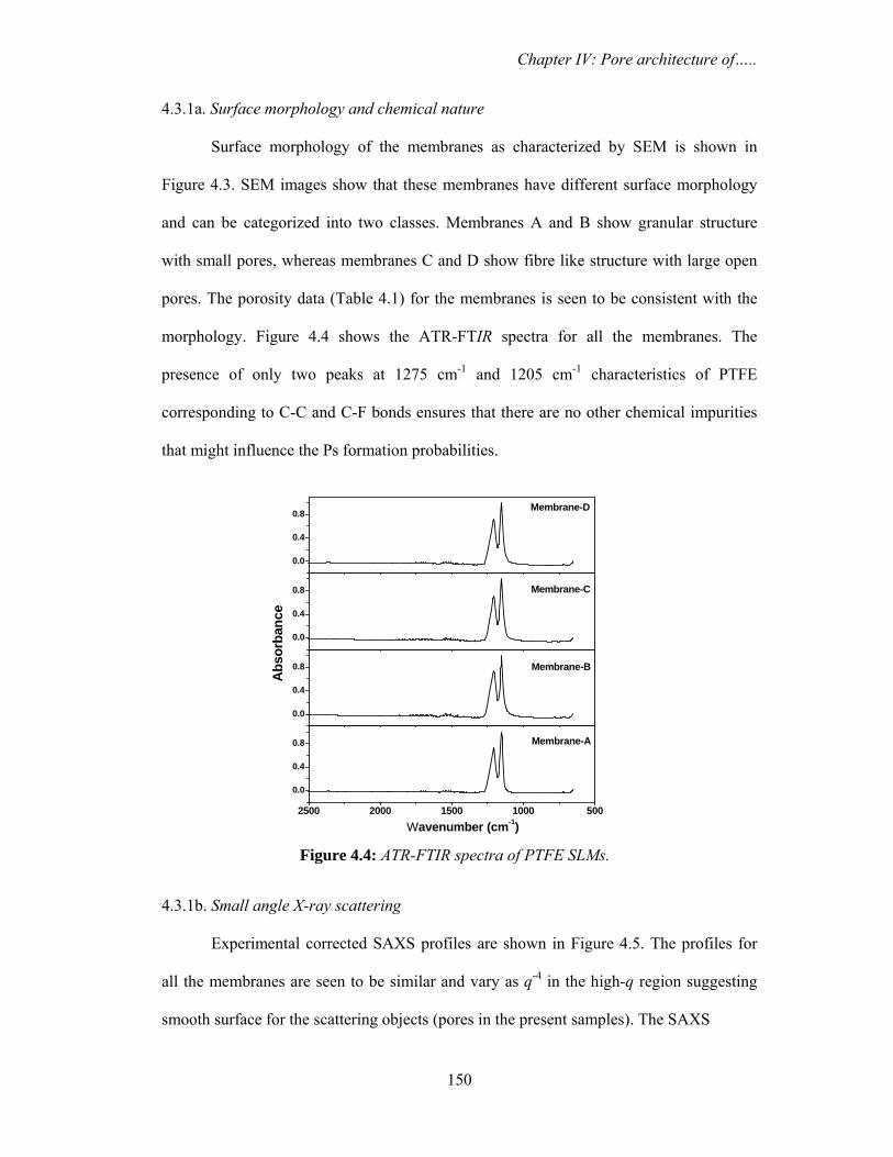
Chapter IV: Pore architecture of…..
150
4.3.1a. Surface morphology and chemical nature
Surface morphology of the membranes as characterized by SEM is shown in
Figure 4.3. SEM images show that these membranes have different surface morphology
and can be categorized into two classes. Membranes A and B show granular structure
with small pores, whereas membranes C and D show fibre like structure with large open
pores. The porosity data (Table 4.1) for the membranes is seen to be consistent with the
morphology. Figure 4.4 shows the ATR-FTIR spectra for all the membranes. The
presence of only two peaks at 1275 cm-1 and 1205 cm-1 characteristics of PTFE
corresponding to C-C and C-F bonds ensures that there are no other chemical impurities
that might influence the Ps formation probabilities.
4.3.1b. Small angle X-ray scattering
Experimental corrected SAXS profiles are shown in Figure 4.5. The profiles for
all the membranes are seen to be similar and vary as q-4 in the high-q region suggesting
smooth surface for the scattering objects (pores in the present samples). The SAXS
Figure 4.4: ATR-FTIR spectra of PTFE SLMs.
0.0
0.4
0.8
2500 2000 1500 1000 500
0.0
0.4
0.8
0.0
0.4
0.8
0.0
0.4
0.8
Wavenumber (cm-1)
Membrane-A
Abs
orba
nce
Membrane-B
Membrane-D
Membrane-C
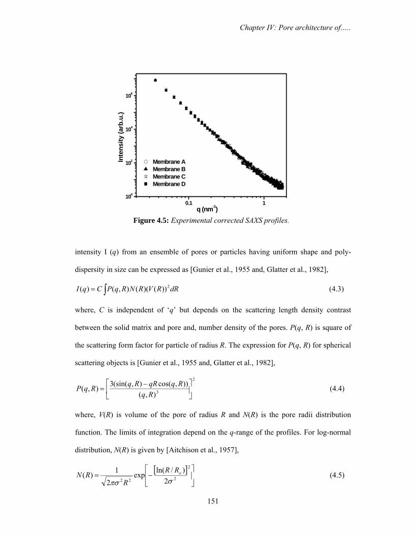
Chapter IV: Pore architecture of…..
151
intensity I (q) from an ensemble of pores or particles having uniform shape and poly-
dispersity in size can be expressed as [Gunier et al., 1955 and, Glatter et al., 1982],
dRRVRNRqPCqI ∫= 2))()((),()( (4.3)
where, C is independent of ‘q’ but depends on the scattering length density contrast
between the solid matrix and pore and, number density of the pores. P(q, R) is square of
the scattering form factor for particle of radius R. The expression for P(q, R) for spherical
scattering objects is [Gunier et al., 1955 and, Glatter et al., 1982],
2
3),()),cos(),(sin(3),( ⎥⎦
⎤⎢⎣
⎡ −=
RqRqqRRqRqP (4.4)
where, V(R) is volume of the pore of radius R and N(R) is the pore radii distribution
function. The limits of integration depend on the q-range of the profiles. For log-normal
distribution, N(R) is given by [Aitchison et al., 1957],
[ ]⎥⎦
⎤⎢⎣
⎡−=
2
222 2)/ln(exp
21)(
σπσoRR
RRN (4.5)
0.1 1100
102
104
106
Inte
nsity
(arb
.u.)
q (nm-1)
Membrane AMembrane BMembrane CMembrane D
Figure 4.5: Experimental corrected SAXS profiles.
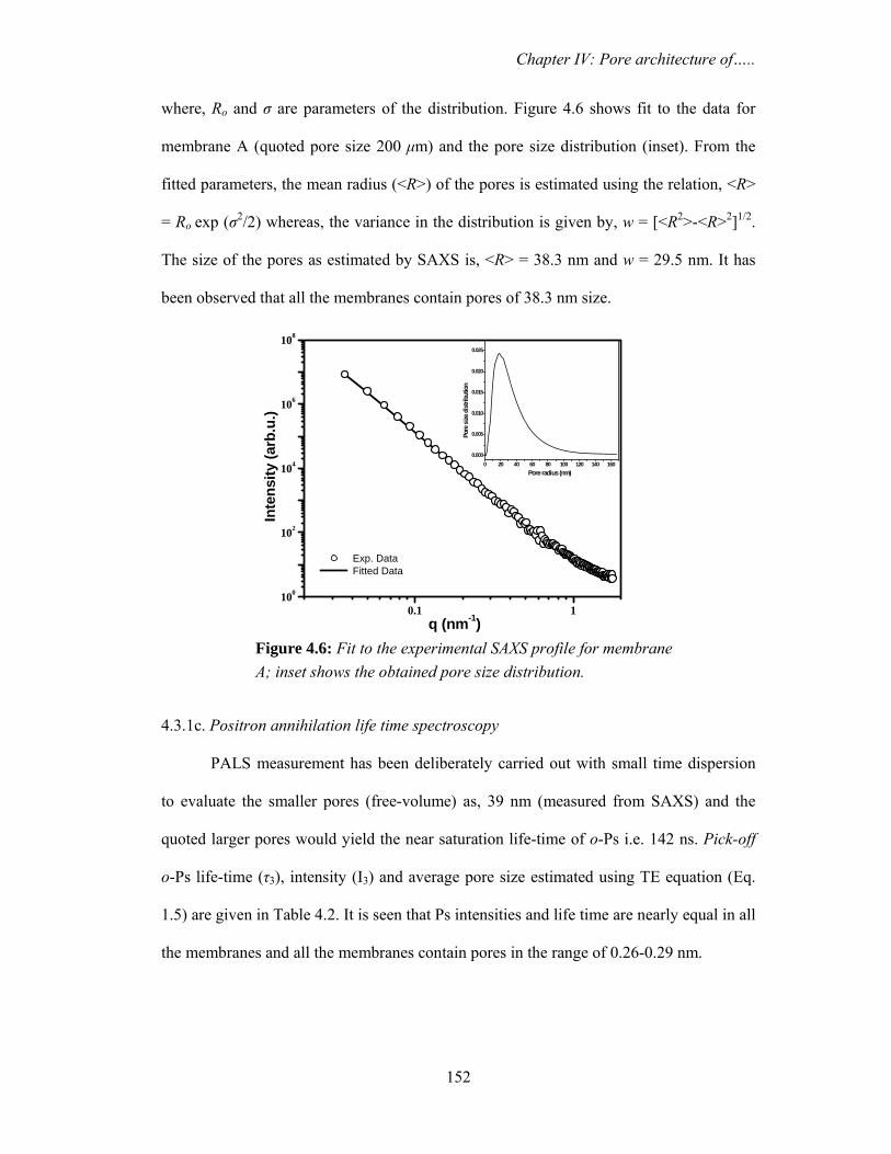
Chapter IV: Pore architecture of…..
152
where, Ro and σ are parameters of the distribution. Figure 4.6 shows fit to the data for
membrane A (quoted pore size 200 μm) and the pore size distribution (inset). From the
fitted parameters, the mean radius (<R>) of the pores is estimated using the relation, <R>
= Ro exp (σ2/2) whereas, the variance in the distribution is given by, w = [<R2>-<R>2]1/2.
The size of the pores as estimated by SAXS is, <R> = 38.3 nm and w = 29.5 nm. It has
been observed that all the membranes contain pores of 38.3 nm size.
4.3.1c. Positron annihilation life time spectroscopy
PALS measurement has been deliberately carried out with small time dispersion
to evaluate the smaller pores (free-volume) as, 39 nm (measured from SAXS) and the
quoted larger pores would yield the near saturation life-time of o-Ps i.e. 142 ns. Pick-off
o-Ps life-time (τ3), intensity (I3) and average pore size estimated using TE equation (Eq.
1.5) are given in Table 4.2. It is seen that Ps intensities and life time are nearly equal in all
the membranes and all the membranes contain pores in the range of 0.26-0.29 nm.
0.1 1100
102
104
106
108
0 20 40 60 80 100 120 140 1600.000
0.005
0.010
0.015
0.020
0.025
Pore
size
dist
ribut
ion
Pore radius (nm)
Inte
nsity
(arb
.u.)
q (nm-1)
Exp. Data Fitted Data
Figure 4.6: Fit to the experimental SAXS profile for membrane A; inset shows the obtained pore size distribution.

Chapter IV: Pore architecture of…..
153
Table 4.2: o-Ps life life-time, Intensity and calculated pore size (PALS measurement)
Membranes o-Ps pick-off lifetime, τ3 (ns)
Intensity, I3 (%)
Radius
(nm)
A 1.92 5.99 0.28
B 1.76 6.22 0.26
C 1.98 7.03 0.29
D 1.82 5.59 0.27
4.3.1d. Doppler broadening and 3γ/2γ annihilation spectroscopy
The S-parameter and 3γ/2γ ratio as a function of positron energy (depth) for all the
membranes (as received/pristine) are shown in Figure 4.7 and 4.8, respectively. The S-
parameter profiles are seen to be flat and no significant difference has been observed for
membranes A, B, C and D. This is similar to the behavior of S-parameter in nonporous
PTFE. Flatness of the profiles in the present case may also be due to the highly porous
nature of the membranes. It is, therefore, not useful in elucidating any information on Ps
0 2 4 6 8 100.54
0.55
0.56
0.57
0.58
0.59
0.60Membrane AMembrane BMembrane CMembrane D
S- p
aram
eter
Positron energy (keV)
Figure 4.7: The S-parameter profile for pristine PTFE SLMs. Error on the data is indicated on one of the data points in the figure.

Chapter IV: Pore architecture of…..
154
mobility. The 3γ/2γ profile (Figure 4.8), on the otherhand, shows distinct changes with
positron incident energy as well as between the membranes. The profiles carry
information about the Ps mobility and fitted using VEPFIT to extract Ps diffusion length
(L+). The fit to the experimental data, represented by solid lines is shown in Figure 4.9.
The diffusion lengths are seen to be 39, 102, 72 and 107 nm for membrane A, B, C and D,
respectively. The obtained diffusion length in the case of membrane C and D are seen to
be very small inspite of the large size of pores as compared to membrane A and B. It is
seen from SEM that membrane C and D have different morphology compared to A and B.
Also, the porosities in the former are larger. From the measured Ps diffusion length it is
seen that although there is a sharp increase in L+ going from A to B, the values for C and
D seem to be underestimated considering the porosity and morphology.
In order to get a better understanding in to this aspect, 3γ/2γ profile for the
membranes B and C (one membrane from either category) with a surface diffusion layer
of gold (10 nm) has been measured. This prevents Ps from escaping in to the vacuum that
0 2 4 6 8 10
0.80
0.84
0.88
0.92
0.96
1.00
3γ
/2γ r
atio
Membrane AMembrane BMembrane CMembrane D
Positron energy (keV)
Figure 4.8: The 3γ/2γ profiles for pristine PTFE SLMs. Error on the data is same for all the membranes and is shown for one of the membranes in the figure.

Chapter IV: Pore architecture of…..
155
might modify 3γ/2γ profile. The 3γ/2γ profile for goldcoated and the pristine membranes
(B and C) are compared in Figure 4.10.
Figure 4.9: VEPFIT analysis of 3γ/2γ ratio for PTFE SLMs. Solid lines represent fit to the experimental data.
0 2 4 6 8 100.80
0.84
0.88
0.92
0.96
1.00
1.04
1.08
3γ/2γ r
atio
Positron energy (keV)
0.80
0.84
0.88
0.92
0.96
1.00
1.04
1.08
Membrane B
Membrane C
Figure 4.10: 3γ/2γ profiles for Pristine and goldcoated PTFE (soild symbols) membranes B and C.

Chapter IV: Pore architecture of…..
156
At thermal velocity, Ps can travel a substantial distance away from the surface
prior to annihilation. Considering the experimental arrangement (detector perpedicular to
sample), Ps escape from the membrane surface due to open surface porosity has resulted
in the decrease in 3γ detection leading to decrese in 3γ/2γ ratio in the surface region. In
the case of membrane C, the open porosity on the surface seems to be much higher than
the membrane B as reflected from the large difference in 3γ/2γ ratio (surface region) in
the former. The fitting of 3γ/2γ profiles obtained in the case of goldcoated membranes
show much higher L+ viz. 400 and 3000 nm for B and C, respectively as compared to 102
and 72 in the corresponding pristine membranes. By preventing Ps to escape from the
surface and make them coral within the membrane reveals the true picture of the pore
architecture of the membranes. The L+ is related to the mean free path of Ps and hence,
measure of pore interonnectivity. The obtained L+ indicate that pore interconnectivity is
much higher in the case of fibrous membranes (C and D) as compared to membrane A
and B having granular structure.
4.3.1.e. Permeability of metal ions and transport properties
Figure 4.11 shows the permeabilty of Pu+3 and Am+3 for all the four membranes
(A, B, C and D) with TODGA as extractant, n-dodecan as solvent and nitric acid in feed
as well as receiver cells. A systematic decrease in permeability is seen from A to D ( i.e.
increase in pore size) under identical condition. Similar trend has also been seen in earlier
studies on the permeation of UO22+ through identical PTFE SLMs [Mohapatra et al., 2006
and Lakshmi et al., 2004]. It is known that permeability is proportional to φR2 (R being
radius of pore) and inversely proportional to the thickness of the membrane [Baker,
2004]. The latter being identical in all the membranes, the permeability should have been
highest in the case of membrane D contrary to what is observed in the present study.

Chapter IV: Pore architecture of…..
157
0.001
0.002
0.003
B DCA
P (c
m/s
ec)
Membrane
L + (nm
)
40
80
120 (c)
(b)
(a)
0.000
0.002
0.004
Am(III)
Pu(III)
Figure 4.12: Correlation between Permeability of ions in PTFE membranes and Ps diffusion length.
0.0005
0.0010
0.0015
0.0020
0.0025
0.0030
0.0035
DCBA
Perm
eabi
lity
(cm
/s)
Membrane
Pu(lll) Am(lll)
Figure 4.11: Permeability of Pu (lll) and Am (lll) through PTFE membranes.

Chapter IV: Pore architecture of…..
158
An inverse correlation between the permeability and L+ has been observed for
PTFE SLMs (Figure 4.12) i.e. higher the L+, lower is the permeability. A systematic
increase in L+ can be ascribed to increase in pore interconnectivity or pore overlap,
resulting in enhancement in the mean free path of the Ps atom. Such interconnection of
pores provides alternative path to the diffusing metal ion complex which could be longer
than the thickness of the membrane it has to travel to reach the receiver compartment.
Overall this would result in increase in the time taken by the metal ions to permeate
through the membrane resulting in decrease in permeability. In the parlance of membrane
science this is referred to as tortuosity. Permeability scales inversely with tortuosity i.e.
higher the tortuosity lower is the permeability [Baker et al., 2004]. Pore interconnectivity
is the main microscopic reason for the increase in the tortuosity in a membrane as evident
from the measured L+. The large pore interconnectivity is seen to have deleterious effect
on the permeability (inverse relation between the two) of metal ions through the
membrane.
Colating all the information from conventional as well as positron beam studies,
an impression of pore architecture of the studied membranes (granular and fibrous) is
depicted in Figure 4.13. As seen, pore overlap increases in the case of fibrous membrane
Figure 4.13: Impression of pore architecture in porous membranes.

Chapter IV: Pore architecture of…..
159
having large size pores, resulting in large interconnectivity between the pores. Also,
fibrous membrane have high open porosity. The solid lines represent the path taken by the
metal ion complex across the membrane. Pore overlap (interconnection) is seen to
provide alternative tortuous path to metal ions resulting in lowering of permeability.
4.3.2. Track etched polycarbonate membranes
4.3.2a. Surface morphology
Figure 4.14a shows the SEM image of one of the track etched nuclepore PC
membranes showing the presence of cylindrical through and through pores. Distinct
morphology of track etched PC membrane as compared to fibrous membrane (PTFE
SLM) having highly interconnected pores is clearly evident from Figure 4.14b. In the
present study PC membranes with pore size 0.03, 0.2 and 0.4 μm are named as membrane
1, 2 and 3, respectively.
4.3.2b. Doppler broadening and 3γ/2γ annihilation spectroscopy
The variation of S-parameter as a function of positron energy for membranes 1-3
are shown in Figure 4.15. The S-parameter profile is almost featureless throughout the
energy range owing to the highly porous nature of the membranes. As the pore size is
large (order of μm) in these membranes, o-Ps pick-off annihilation is expected to be
Figure 4.14: SEM images of (a) track etched PC and, (b) fibrous PTFE SLM. Yellow lines indicates the length scale of measurement; (a) 6 μm; (b) 50 μm

Chapter IV: Pore architecture of…..
160
insensitive to the pore sizes and most of the o-Ps annihilate by 3γ annihilation. The
energy spectroscopy (3γ/2γ), which directly senses the formation and complete history of
long-lived 3γ decay of o-Ps, is seen to be a more sensitive technique for the investigation
of pore architecture in these membranes. In addition, similar to earlier observation in
PTFE SLMs, open porosity due to large pore size may modify the 3γ/2γ profiles and
hence, corresponding goldcoated membranes are also studied in order to get true picture
of pore architecture in these membranes. The 3γ/2γ profiles for PC membranes are shown
in Figure 4.16 indicating distinct variation between the membranes. The quantitative
analysis for the observed variations is carried out by evaluating L+ using VEPFIT. The L+
obtained by fitting the 3γ/2γ profiles are 55, 30 and 76 nm for membrane 1, 2 and 3,
respectively. No systematic trend in L+ is seen with the increase in the pore size. Based
on our earlier observations (PTFE SLMs), for large size pores (micron range) and highly
porous membranes, the escape of Ps from the surface modifies the profiles resulting in
underestimation of L+. In such cases, true pore architecture can be obtained by capping
the membrane surface with gold layer to prevent Ps escape from the surface. The S-
0 4 8 12 16 200.52
0.53
0.54
0.55
0.56
0.57
0.58
0.59
0.60 Membrane 1 Membrane 2 Membrane 3
S-pa
ram
eter
Positron energy (keV)
Figure 4.15: The S-parameter profile for pristine track etched PC membranes; Membrane 1 (0.03 μm), Membrane 2 (0.2 μm) and Membrane 3 (0.4 μm).

Chapter IV: Pore architecture of…..
161
Figure 4.16: 3γ/2γ profiles for pristine track etched PC membranes.
0 4 8 12 16 20
0.76
0.80
0.84
0.88
0.92
3γ/2γ r
atio
Positron energy (keV)
Membrane 1 Membrane 2 Membrane 3
parameter and 3γ/2γ profile for goldcoated PC membranes are shown in Figures 4.17 and
4.18, respectively. No significant variation is S-parameter with depth has been observed
owing to the porous nature of the membranes and hence, it cannot be used to elucidate
any information about the pore architecture. However, it indicates that Ps yield in all the
membranes is same. On the otherhand, 3γ/2γ profiles for goldcoated membranes show
distinct behavior as compared to their pristine forms. The measured L+ for goldcoated
membrane 1, 2 and 3 are 375, 255 and 330 nm, respectively.
0 2 4 6 8 10 12
0.58
0.59
0.60
0.61
0.62
0.63 Membrane 1 Membrane 2 Membrane 3
S-pa
ram
eter
Positron energy (keV)
Figure 4.17: The S-parameter profile for goldcoated PC membranes.
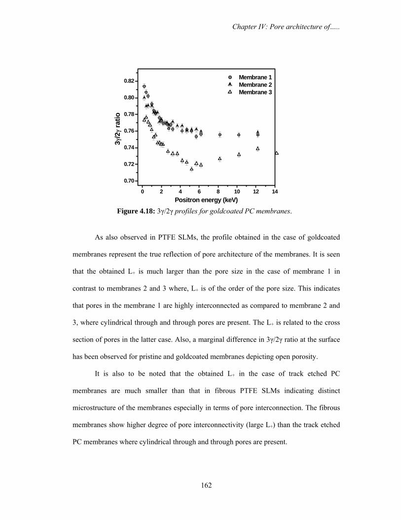
Chapter IV: Pore architecture of…..
162
As also observed in PTFE SLMs, the profile obtained in the case of goldcoated
membranes represent the true reflection of pore architecture of the membranes. It is seen
that the obtained L+ is much larger than the pore size in the case of membrane 1 in
contrast to membranes 2 and 3 where, L+ is of the order of the pore size. This indicates
that pores in the membrane 1 are highly interconnected as compared to membrane 2 and
3, where cylindrical through and through pores are present. The L+ is related to the cross
section of pores in the latter case. Also, a marginal difference in 3γ/2γ ratio at the surface
has been observed for pristine and goldcoated membranes depicting open porosity.
It is also to be noted that the obtained L+ in the case of track etched PC
membranes are much smaller than that in fibrous PTFE SLMs indicating distinct
microstructure of the membranes especially in terms of pore interconnection. The fibrous
membranes show higher degree of pore interconnectivity (large L+) than the track etched
PC membranes where cylindrical through and through pores are present.
Figure 4.18: 3γ/2γ profiles for goldcoated PC membranes.
0 2 4 6 8 10 12 14
0.70
0.72
0.74
0.76
0.78
0.80
0.82 Membrane 1 Membrane 2 Membrane 3
3γ/2γ r
atio
Positron energy (keV)

Chapter IV: Pore architecture of…..
163
4.4. Conclusions
The pore architecture of supported liquid PTFE and track etched PC membranes
having micron size pores have been studied using PAS. Slow positron beam depth
profiling has been utilized to evaluate Ps mobility (diffusion length) in these membranes
defined by the mean free path of Ps in the system. This has been utilized to evaluate pore
architecture in terms of pore interconnectivity in these membranes. Ps diffusion length, a
measure of length of interconnection of the pores is evaluated from the 3γ/2γ profiles
using VEPFIT analysis. The high open porosity at the surface has been seen to modify
3γ/2γ profiles due to the escape of Ps from the surface and do not represent the true pore
architecture. Capping the surface of the membrane with thin gold layer prevents the
escape of Ps from the surface and hence, gives a true reflection of the pore architecture of
the membranes. In the case of PTFE SLMs, high interconnectivity has been observed for
the fibrous class of the membrane (C and D) as compared to the granular (A and B). An
inverse correlation between the pore interconnectivity and the permeability of metal ions
through SLMs has been observed. High interconnectivity results in decrease in
permeability. The increase in tortousity due to large interconnectivity is responsible for
the decrease in permeability. On the otherhand, in the case of track etched PC membranes
having through-and-through cylindrical pores, the interconnectivity between the pores is
seen to be less than the PTFE SLMs. It is also observed that, in the case of less
interconnected but large size pores, Ps diffusion length is a measure of cross section
rather than length of the pores. PAS is one of the best probes to measure pore sizes in the
range of 0.1-1 nm. However, for polymeric systems having large size and interconnected
pores, slow positron beam depth profiling provide an approach to measure pore
architecture of the membrane especially in terms of open porosity and length of
interconnection between the pores. The pore architecture of the membrane is the

Chapter IV: Pore architecture of…..
164
microscopic origin of the transport properties of the membranes. The study demonstrates
the advantages of positron beam characterization of pore interconnectivity in the
design/development of membranes with tailored transport properties.
Chapter V: Nanostructure characterization……
165
CHAPTER-V
Nanostructure characterization in
Organic Semiconductor thin films

Chapter V: Nanostructure characterization……
166
Organic thin film devices are the primary building block for the next generation
organic electronics. Owing to the dependence of electronic, optical and even magnetic
properties on the structure and morphology of the films, the ordered, smooth and defect
free surfaces are prerequisite for achieving high performance electronic devices
[Stadlober et al., 2006; Offerman et al., 2002]. The growth behavior of OSC molecules
depends on the nature of substrate, its temperature, deposition technique, rate of
deposition and post deposition annealing treatment [Karan et al, 2007; Miller et al., 2005;
Forrest et al., 1997; Nonaka et al., 1995]. There have been number of studies using
variety of techniques addressing the growth behavior and its effect on the performance of
organic devices [Don Park et al., 2007; Koch et al., 2007]. For example, nature and
temperature of the substrate affects the growth mode of organic molecules. The
interaction between the substrate and the molecules as well as between the two molecules
dictates molecular arrangement. When substrate-molecule interaction dominates, stacking
of the molecules will be edge-on. However, molecules stack in face-on manner if
molecule-molecule interaction is dominant [Debnath et al., 2008]. In addition to this,
heteroepitaxy between different materials results in translational and orientational
domains, which are the sources of disorder/defects at the interfaces between different
materials [Brutting et al., 2008]. These defects may influence charge transport properties
of the devices. Therefore, optimization of growth parameters/conditions and the
characterization of structural properties are very relevant to organic electronic industry.
Several techniques are used for structural characterization of these devices. For instance,
AFM and SEM are often used for the characterization of surface morphology
[Chowdhury et al., 2012; Virkar et al., 2010], sputter-ion based X-ray photoelectron
spectroscopy (XPS) [Hong et al., 2012; Liu et al., 2011] and secondary ion mass
spectrometry (SIMS) for compositional characterization [Chang et al., 2012], near-edge

Chapter V: Nanostructure characterization……
167
X-ray absorption fine structure (NEXAFS) for bond orientation and chemistry of the film
and Grazing incidence X-ray diffraction (GIXRD) for crystal structure. However,
destructive nature (sputter-ion XPS, SIMS) and limited depth profiling capability
(GIXRD) impose limitations on the utilization of these techniques for the characterization
of organic devices. In addition, only few techniques are available which can provide
defect structure of the film and interfaces. AFM and SEM are sensitive to structural
defects, but these are local probes for the characterization of surface morphology only and
cannot provide information about the nanostructure of buried layers and interfaces.
Depth profiling using slow positron beam has emerged as a sensitive technique for
the characterization of defect microstructure in thin films. The sensitivity of positrons to
get trapped in low electron density regions enables study of open volume defects and
vacancies. Together with the ability to monoenergize positrons helps in probing defect
microstructure at different depths of the sample. In the present work, the technique has
been employed for the first time for defect depth profiling in OSC thin films. The growth
behavior and surface morphology in OSC thin films are mainly characterized by AFM
and SEM. However, there are no studies related to depth dependent defect microstructure
in these films especially, interfacial microstructure which requires either layer by layer
sputtering or growth of monolayers. The defect microstructure of different layers and
interfaces in actual device configuration cannot be probed by these techniques due to the
destructive nature of the techniques. In this context, defect depth profiling is useful to
investigate structural inhomogeneities as well as interfaces in organic devices.
In the present work, defect depth profiling has been carried out in OSC thin films
under different growth parameters to examine the nanostructure of the films. Positron
annihilation parameters (S-parameter and diffusion length) are indexed to represent the
nanostructural variations as a function of growth parameters. In the case of films

Chapter V: Nanostructure characterization……
168
subjected to post-deposition annealing, depth profiling has been seen to be sensitive to
structural inhomogeneities in the direction normal to the surface of the film. Depth profile
study has also enabled identification of buried interfaces i.e. interfaces between organic-
organic and organic-inorganic materials in heterostructures. No other technique has been
seen to be sensitive to defect/disorders present in these interfaces.
The growth behavior of organic molecules depends on the interaction between the
molecules and the dielectric surface. The surface energy/roughness of dielectric strongly
influences the nucleation and growth of molecules, grain size, molecular ordering and
crystalline structure. These factors are crucial for the mobility of charge carriers in
organic devices. Interface engineering has been employed to modify dielectric surface
(substrate) using self assembled monolayer in order to improve the growth behavior of
OSC to achieve high charge mobility. The present study pertains to the investigation of
defect microstructure of the interface between dielectric substrate
(modified/unmodified)/OSC layer and its effect on the charge carrier mobility. The above
study using positron beam has been corroborated with other conventional characterization
techniques like AFM, GIXRD and X-ray reflectivity (XRR).
5.1. Material and sample preparation
In this work, metal phthalocyanines (MPcs) have been used as OSC materials.
Phthalocyanines (Pc’s) are a class of planar aromatic organic compounds which exhibit
semiconductor properties. Their thermal and chemical stability makes them very suitable
material for organic electronic devices [Ribeiro et al., 2000; Prince et al., 2001]. MPcs
have planar (within 0.3 Å) molecular structure, as schematically shown in Figure 5.1. The
parent molecule, hydrogenated Pc, with chemical formula C32H18N8, has 2 hydrogen
atoms in the center of the ring, and 16 surrounding the molecule. The two hydrogen
atoms are replaced by a metal atom in case of MPcs. The replacement of central metal

Chapter V: Nanostructure characterization……
169
atom and side group modifies the electronic properties of Pcs. For example CuPc is a p-
type organic semiconductor but the replacement of 16 hydrogen by fluorine makes the
molecule (F16CuPc) n-type.
Thin films of different MPcs have been used as organic semiconductor materials
in the present work. The effect of substrate temperature and thickness of the film on the
nanostructure of the films have been studied for Iron-Phthalocyanine (FePc). FePc films
of thicknesses 50, 100 and 140 nm have been grown on ITO-glass substrate by molecular
beam epitaxy technique using RIBER make model EVA32 system. These films have been
deposited using an effusion cell loaded with 97% pure α-FePc powder (Aldrich make) at
substrate temperature of 200oC. The above method has also been utilized for the
deposition of FePc films at two different temperatures viz. 30oC and 300
oC.
The effect of post-deposition annealing has been studied for cobalt-
phthalocyanine (CoPc) film grown on quartz substrate by thermal evaporation using Hind
high Vac thermal evaporation system (model no-12A4T) under vacuum better than 10-6
mbar. The substrate is cleaned by sonication with trichloroethylene, acetone and methanol
separately for 5 minutes each before the deposition. The film is deposited at room
temperature at the deposition rate of 0.2-0.3 Å/sec. The thickness of the film as measured
by quartz crystal monitor is 200 nm. The grown film has been subjected to post-
• Metal atom
• Nitrogen atom
• Carbon atom
Figure 5.1: The structure of Metal Phthalocyanine molecule.

Chapter V: Nanostructure characterization……
170
deposition annealing treatment at temperatures 140 and 200○C in a vacuum oven for 1
hour in a vacuum better than 10-3
mbar.
For the study of interfacial characteristics in OSC heterostructures, single layer
and multilayer films of n-type (copper-hexadecafluoro-phthalocyanine, F16CuPc) and p-
type (cobalt-phthalocyanine, CoPc; FePc and zinc-phthalocyanine, ZnPc) OSC materials
have been prepared on quartz substrate by thermal evaporation using Hind high Vac
thermal evaporation system (model no-12A4T) under vacuum better than 10-6
mbar. The
substrate is cleaned by sonication with trichloroethylene, acetone and methanol separately
for 5 minutes each before the deposition. Films have been deposited at the substrate
temperature of 100o
C and the deposition rate of 0.2 Å/sec. The thickness of single layer
films of n-type (F16CuPc) and p-type (CoPc) material is 80 nm thick. The multilayer
structures comprise bilayer of p-n (CoPc- F16CuPc) and p-p (FePc- ZnPc) type and
trilayer of n-p-n (F16CuPc- CoPc-F16CuPc) type OSC materials. The thickness of each
film in bilayer and trilayer structures is 60 nm and 30 nm, respectively. The thickness of
the films has been measured by quartz crystal monitor.
Interface engineering of dielectric surface (SiO2/Si) has been carried out using self
assembled monolayers (SAM) of trichlorosilane viz. phenyhexyltricholorosilane (PTS)
and octadecyltrichlorosilane (OTS) differing in the tail group and chain length. Highly
doped n-type (100) Si wafer has been used as a substrate and the gate dielectric SiO2 of
200 nm thickness has been deposited thermally. For modifying SiO2 with SAM of OTS,
silicon substrates with SiO2 layer has been first cleaned in Piranha solution (2:1 v/v
H2SO4 and H2O2) to obtain OH terminated surface and then immersed in freshly prepared
0.5 mM OTS solution in toluene for 16 hours in an argon filled glove box (relative
humidity and oxygen < 1 ppm). For the preparation of PTS (phenylhexyltrichlorosilane)
SAM, SiO2 substrates has been immersed in freshly prepared 0.25 mM

Chapter V: Nanostructure characterization……
171
phenylhexyltrichlorosilane (PTS) solution in toluene for 3 hours. Thickness of the
monolayers (OTS ~2.6 nm; PTS~1.4 nm) has been measured using ellipsometry. CuPc
films have been grown on native oxide SiO2 (3-4 nm)/Si, thermally grown oxide SiO2
(200 nm)/Si and SAM modified SiO2 (200 nm)/Si substrates using thermal evaporation
using Hind high Vac thermal evaporation system (model no-12A4T) under vacuum better
than 10-6
mbar. The deposition rate has been maintained at 0.5-1 Å/s and thickness of the
films is about 30 nm, as measured by quartz crystal monitor. The schematic of different
SAM (PTS and OTS) and SAM modified substrate with a grown OSC layer is shown in
Figure 5.2.
Figure 5.2: Schematic of (a) OSC grown on self assembled monolayer (SAM) modified
SiO2/Si substrate; (b) PTS; (c) OTS.
Chapter V: Nanostructure characterization……
172
5.2. Experimental Techniques
5.2.1. Grazing incidence X-ray diffraction (GIXRD)
The nature of the grown films (crystallinity) has been determined using GIXRD.
The measurements have been carried out using PANalytical MRD system using Cu Kα
radiation of wavelength 0.15418 nm in out of plane geometry. The measurements have
been performed at small grazing angles (0.2o to 1
o) with a high resolution theta-2-theta
scan ranging from 0o to 15
o in the step size of 0.0001° to examine the crystalline nature of
the films. However, in the case of heterostructures (multilayer films), measurements are
performed at varying grazing angles so as to probe the multilayer system as a function of
depth. The high resolution theta-2-theta scan ranging from 0o to 30
o in the step size of
0.0001° is carried out at each grazing angle.
5.2.2. Atomic force microscopy (AFM)
The surface morphology of the films have been characterized using AFM in
tapping/non-contact mode. The measurements are performed using a NT-MDT solver
model instrument with 50 μm scanner head and silicon nitride tip with a scanning speed
of about 1 Hz. The growth mode of CuPc molecules grown on SiO2 (200 nm)/Si at room
temperature and 225oC have been examined by depositing only one or two monolayers
(~ 2 nm) of CuPc on the modified substrate.
5.2.3. Doppler broadening spectrosocpy
Depth profiling has been carried out using Doppler broadening spectroscopy using
slow positron accelerator at Radiochemistry Division, Bhabha Atomic Research Centre,
Mumbai. The depth dependent Doppler broadening measurements have been carried out
in the positron energy ranging from 200 eV to the maximum of 20 keV. A high purity
germanium detector with a resolution of 2.0 keV at 1332 keV photopeak of 60
Co has been

Chapter V: Nanostructure characterization……
173
used for Doppler broadening measurements and approximately half a million counts are
acquired under 511 keV photopeak at each energy. The Doppler broadened annihilation
-radiation has been characetrized by line shape parameters S and W. The S-parameter
mainly reflects the change due to positron annihilation with electrons having low
momentum distribution, whereas, W-parameter reflects the annihilation from electrons
with high momentum distribution. The ratio of integral counts within ~ 2.0 keV energy
window centered at 511 keV to the total photo peak area has been used to evaluate S-
parameter, whereas, W-parameter is evaluated from the energy window of ~ 5 keV in the
wing region of 511 keV photopeak. The S-W correlation has been examined to identify
the nature and type of defects in multilayers. VEPFIT analysis has been used to fit S-
parameter profiles as a function of energy of the positrons to evaluate S-parameter and
positron diffusion length in the layers and interfaces, as the case may be. Positron
mobility in organic layers has also been calculated from the fitted value of positron
diffusion length.
5.2.4. Current-voltage measurement (J-V characteristics)
The current density-voltage (J-V) measurements have been carried out using two
probe in-plane electrode geometry as shown in Figure 5.3. Two planar gold electrodes of
Figure 5.3: A schematic of in-plane charge transport measurement geometry.
Chapter V: Nanostructure characterization……
174
length 3 mm, width 2 mm separated by 12 μm are thermally deposited onto the films
using a metal mask and silver wires are attached to the gold pads with silver paint. J-V
measurements are carried out using Keithley 6487 picoammeter/ voltage source and
computer based data acquisition system.
5.2.5. X-ray reflectivity (XRR)
When X-ray beam falls on a surface it undergoes total external reflection below
certain critical angle (θc). Above θc, X-ray starts penetrating inside the layer and the
reflectivity of the sample falls off with a slope depending on the incidence angle and the
roughness of the interface. The oscillation on the reflectivity spectrum above θc (generally
known as the Kiessig oscillations) is due to the finite thickness of the layer. The
reflectivity pattern is obtained from the interference of monochromatic X-rays that are
reflected from the different interfaces of the layered structure, owing to the changes in
refractive indices of the layers. When used in specular (angle of incidence=angle of
reflection) mode, XRR can provide information regarding the structure of the layers
through an electron density profile in a direction normal to the surface [Pietsch et al.,
1993; Xia et al., 2004]. In this configuration these experiments probe the electronic
density that is roughly homogeneous in the horizontal plane but varies in a deterministic
way along the vertical depth of the sample. In general, the thickness of the film can be
obtained from the frequency of oscillations, while the slope of the curve gives the
roughness of the interface.
X-ray reflectivity measurements have been carried out using CuKα radiation (1.54
Å) on a computer-controlled reflectometer (Kristalloflex 710 D X-ray generator
(SIMENS) and D5000 diffractometer). The complex index of refraction for X-rays is
given by,
= 1- (re e 2/2 ) – i ( /4 ) (5.1)

Chapter V: Nanostructure characterization……
175
where, re (= 2.818 fm) is the classical electron radius; e is the electron scattering length
density of the material (in Å-2
units), is the incident wavelength (in this case: Cu K ,
1.54Å) and is the absorption coefficient. Since is usually < 1, total external reflection
of X-rays will occur at the surface of the material under study for grazing incident angle θ
smaller than the critical angle θc, whose value depends on the electron density. Therefore,
the value of θc is specific to a material. Above the critical angle, X-rays can penetrate the
material up to a depth determined mainly by the absorption coefficient. In the case of a
single thin film on a substrate, for θ > θc , reflection occurs at both the air/film and
film/substrate interfaces due to differences in refractive indices or electron densities of the
layers (called density contrast). The combination of both these reflections results in
interference fringes. Such interference patterns are recorded as a function of momentum
transfer q (Å−1
) perpendicular to the reflecting surface, where q = (4 / ) sin θ. The
lessening or absence of interference fringes in a reflectivity pattern can be attributed to
variations like surface/interface roughening, interdiffusion or formation of interface
layers. In order to obtain meaningful information from the measured reflectivity, the
experimentally obtained data is fitted with a computer generated theoretical model, from
which one can derive depth-dependent scattering length density (SLD) profile of the
sample. The fitting parameters used which ultimately define the sample are thickness,
electron density and roughness for each layer. Thus, it is obvious that SLD, which is the
product of number density per unit volume of the constituents and the Thomson scattering
length for X-rays, contains significant information for the characterization of a material,
especially with respect to vertical depth.
5.3. Results and Discussion
5.3.1. Effect of substrate temperature and thickness of the film
5.3.1a. Surface morphology and crystallinity

Chapter V: Nanostructure characterization……
176
The effect of deposition temperature (substrate) and thickness of the film on the
nanostructure has been studied for FePc thin films. The crystalline nature and surface
morphology of the films have been characterized using GIXRD and AFM. Figure 5.4
shows the GIXRD pattern of FePc films (100 nm) deposited at two different substrate
temperatures (30oC and 300
oC). It is seen that the films grown at substrate temperature of
30oC and 300
oC are amorphous and crystalline, respectively. The films grown at higher
temperature shows crystalline nature owing to the sufficient energy provided to the
molecules to get arranged in an ordered manner on the substrate. To study the effect of
thickness, FePc films of varying thicknesses (50, 100, 140 nm) have been grown at a
substrate temperature of 200oC (all are crystalline films).
5 10 15 20 25 30
0
1500
3000
45000
100
200
300
Inte
nsity
Crystalline film
2 theta
Amorphous film
AFM images and the corresponding height profiles of crystalline FePc films
grown at 200oC are shown in Figure 5.5, depicting significant difference in the
morphology of the films. The film of lowest thickness (50 nm) has shown columnar
growth of molecules, leaving a large open volume ~ 1 m between the columns (as
depicted from AFM height profiles). However, at higher thicknesses, a transition from
Figure 5.4: GIXRD pattern for FePc films grown on ITO-glass
substrate at 30oC (amorphous) and 300
oC (crystalline).

Chapter V: Nanostructure characterization……
177
columnar to granular arrangement has been observed. The free open space between the
molecules at lower thickness gets filled by other molecules with the increase in the film
thickness resulting in random growth of the grains.
5.3.1b. Doppler broadening spectroscopy
The nanostructure variation in the films has been probed by defect depth profiling
using slow positron accelerator. Doppler broadening S-parameter as a function of
implantation depth of the positrons (S-E profile) has been measured for all the films. The
S-E profile has been fitted using VEPFIT analysis to evaluate bulk S-parameter and
positron diffusion length in the films. Figure 5.6 shows S-E profiles for FePc films grown
at 30 and 300oC representing amorphous and crystalline nature, respectively. The higher
value of S-parameter for amorphous film shows the presence of more free volume or
grain boundaries as compared to the crystalline film. The S-E profile is almost flat in the
case of amorphous film depicting large number of defects or voids throughout the film.
These defects act as trapping site for positrons and thus restricting the diffusion of
Figure 5.5: AFM images and height profiles of FePc films.

Chapter V: Nanostructure characterization……
178
positrons in the film (very short positron diffusion length). On the other hand, the
crystalline film shows lower S-parameter in FePc layer as compared to amorphous film.
This indicates that crystalline film has only fewer sites for positron trapping with
comparatively closed packed structure.
S-E profiles for the films with varying thicknesses are shown in Figure 5.7. The profiles
clearly indicate the crystalline nature of the films. The S-parameter at the substrate is
normalized to 1 and the profiles are fitted using VEPFIT analysis to determine S-
parameter and positron diffusion length (Table 5.1). This helps in the identification of
nanostructural variations in the films. The S-parameter at the surface and in the bulk of
FePc layer of the films has been seen to be increasing with the increase in thickness of the
films (Table 1). The positron diffusion length is nearly identical for 50 and 100 nm films,
unlike 140 nm film where, a small but significant (reproducible) decrease has been seen.
The increase in S-parameter and decrease in positron diffusion length have indicated the
increase in trapping sites for positrons with the increase in the thickness of the films.
0 1 2 3 4 5 6
0.95
0.96
0.97
0.98
0.99
1.00
1.01
1.02
SubstrateOSC layer
S-p
ara
mete
r
Positron Energy (keV)
crystalline film
Amorphous film
Figure 5.6: The S-parameter profile for 100 nm thick amorphous
and crystalline FePc films grown at 30 and 300o C, respectively.

Chapter V: Nanostructure characterization……
179
Film
thickness
(nm)
Surface
S-parameter
Bulk
S-parameter
Positron diffusion
length (nm)
50 0.9815 0.9836 17.84 6.96
100 0.9839 0.9909 17.63 5.86
140 0.9902 0.9942 14.61 6.64
5.3.1c. Discussion
As the film thickness increases, molecular arrangement changes from columnar
(rod like) to granular kind with random grain growth resulting in the increase in grain
boundaries. This signifies that the arrangement of molecules and hence, the morphology
of the film depends on the interaction between the substrate and the molecules as well as
between the two molecules. When substrate-molecule interaction dominates stacking of
the molecules will be edge-on. However, molecules stack in face-on manner if molecule-
molecule interaction dominates [Debnath et al., 2008].
Table 5.1: S-parameter and diffusion length (L+) of positron in FePc layer
calculated by VEPFIT.
Figure 5.7: The S-parameter profile for FePc films of different thicknesses.
0 2 4 6 8 10 12 14 16 18
0.980
0.985
0.990
0.995
1.000
1.005
S-p
ara
me
ter
Positron energy (in keV)
film 1 (50 nm)
film 2 (100 nm)
film 3 (140 nm)

Chapter V: Nanostructure characterization……
180
The grain boundaries between the columnar grains in 50 nm film are found to be 1
m in size as reflected from AFM height profile measurement. However, the lowest value
of S-parameter for 50 nm film implies that at lower thickness, columnar arrangement of
molecules has lesser defects as compared to higher thicknesses where molecules arrange
with random grain growth. However, it may also be noted that the micron size inter-
columnar space in 50 nm film as observed through AFM cannot be probed by the
positrons. As the film thickness increases, the inter-granular space is filled by FePc
molecules, leading to more interfaces which act as positron trapping sites. This has
resulted in the increase in S-parameter and decrease in Positron diffusion length with the
increase in the thickness of the films.
5.3.2. Effect of post deposition annealing treatment
5.3.2a. Surface morphology and crystallinity
GIXRD has been used to examine the crystalline nature of CoPc film before and
after annealing at two different temperatures (140 and 200oC). Figure 5.8 shows GIXRD
pattern of as-deposited (film 1) and annealed films (film 2: 140○C and film 3: 200
○C).
The sharp Bragg peak at 6.8o indicates the crystalline nature of the films. This peak
4 6 8 10 12
Film 1: as prepared
Film 2: 140oC annealed
Film 3: 200oC annealed
Inte
nsit
y (
arb
. u
nit
s)
2 (degree)
Figure 5.8: GIXRD pattern of CoPc films

Chapter V: Nanostructure characterization……
181
corresponds to (200) peak of α–CoPc phase. No phase transformation of CoPc has been
observed at the studied annealing temperatures (140 and 200oC).
The surface morphology of the film has been studied using AFM. Figure 5.9
represents AFM images and typical height profiles for the film 1-3. AFM image for film 1
shows smooth island-like structure as also depicted from the broad nature of the height
profile. On the other hand, distinct morphological features start to appear when the film is
annealed at higher temperatures. The high temperature annealing leads to the formation of
grains as clearly seen in AFM images of film 2 and 3. A more homogeneous distribution
of grains has been observed for 200oC annealed film (film 3) as reflected from the sharp
oscillatory behavior of the height profile as compared to film 2. The rms roughness values
for film 1, 2 and 3 are seen to be 3.12, 4.25 and 3.08 nm, respectively. This indicates that
formation of grains initially increases the roughness of the film.
(a) (c) (b)
Figure 5.9: AFM images of CoPc films: (a) as-prepared; (b) annealed at 140oC;
(c) annealed at 200oC

Chapter V: Nanostructure characterization……
182
5.3.2b. Doppler broadening spectroscopy
The variation of S-parameter, as a function of positron implantation energy (S-E
profile) for as-deposited and annealed films (film 1-3) are shown in Figure 5.10. At
higher positron energies (E > 6 keV) S-parameter for all the films corresponds to quartz
substrate. The S-parameter profile for as-deposited (film 1) and film annealed at 140oC
(film 2) are identical, the latter having lower S-value corresponding to OSC region. The
flat response of S-parameter at lower energies for film 1 and 2 indicates the presence of
large number of trapping sites or defects in the film. The low value of S-parameter in film
2 has been attributed to the change in the morphology of the film due to post deposition
annealing. The S-parameter profile for film 3 is seen to be noticeably different than the
film 1 and 2 (Figure 5.10). The profile shows enhancement in S-value at a certain depth in
the region corresponding to the OSC film. The enhancement in S-parameter indicates the
presence of more defects or disorder at the corresponding depth. The quantitative analysis
of the observed differences in S-parameter profiles has been carried out using VEPFIT as
discussed in the following section.
0 2 4 6 8 10 12
0.455
0.460
0.465
0.470
0.475
0.480
0.485
Film 1
Film 2
Film 3
S-p
ara
mete
r
Positron energy (keV)
Figure 5.10: S-parameter profiles for Film 1: as-prepared;
Film 2: annealed at 140oC and Film 3: annealed at 200
oC.

Chapter V: Nanostructure characterization……
183
5.3.3c. VEPFIT analysis
A quantitative analysis of the nanostructural variations in the films has been
carried out by indexing S-parameter and diffusion length of positrons (L+) in the films,
obtained by fitting the S-parameter profiles using VEPFIT analysis [van Veen et al.,
1990]. It has been observed that profiles for film 1 and 2 are best fitted using two layers
in contrast to four layers in the case of film 3. The two layers in film 1 and 2 correspond
to OSC layer and the substrate. However, in film 3, in addition to substrate, the OSC layer
is divided into three distinct layers. The graphical representation of different layers and
corresponding S-values for all the films is shown in Figure 5.11. The fitted values of S-
parameter and L+ for these layers and corresponding thicknesses are given in Table 5.2 (a,
b). S-parameter and L+ for the substrate have been obtained by fitting the experimentally
observed S-parameter profile of the substrate (measured separately). The obtained L+ for
substrate was 20 nm and is used as a fixed parameter for the fitting procedure in the case
of OSC films (film 1-3).
0.450
0.455
0.460
0.465
0.470
0.475
0.480
Film 1
Film 2
0 50 100 150 200 250 300
0.42
0.44
0.46
0.48
0.50
0.52
0.54 Film 3
Substrate
Su
bstr
ate
Layer thickness (nm)
S-p
ara
mete
r
Figure 5.11: VEPFIT fitted S-parameter corresponding to different layers of the films.

Chapter V: Nanostructure characterization……
184
S1
L+1
(nm)
ρ1
(g/cc)
x1*
(nm) S2
L+2
(nm)
ρ2
(g/cc)
Film 1 0.4653±0.0002 1.0 1.76 245± 12 0.4785 (fixed)
21 (fixed)
2.60
Film 2 0.4601±0.0002 3.0 1.76 247± 10 0.4785 (fixed)
21 (fixed)
2.60
* x1 is the layer boundary or width of OSC layer in film 1 and 2
Layer 1 Layer 2 Layer 3 Layer 4
(substrate)
Width of the
layer 106 8 60 ----
S 0.4350
±0.004 0.5162 ± 0.006 0.4326 ± 0.003 0.4801 (fixed)
L+ (nm) 40 4.8 10 18 (fixed)
ρ (g/cc) 1.76 1.65 1.76 2.6
The high S-parameter and short L+ for film 1and 2 indicate disorder or the presence of
large number of defects in the films. In the film 3, however, distinct nanostructure is
clearly revealed from the presence of three OSC layers in contrast to only single OSC
layer in film 1 and 2. Three layers as observed from the fitting in film 3 have different S-
parameter and L+ (Table 5.2b), indicating inhomogeneous nature of the film along the
direction normal to the surface. The S-parameter value for layers 1 and 3 of film 3 are
lower than that of film 1 and 2. The corresponding L+ are also seen to be higher than that
observed in film 1 and 2. The reduction in S-parameter and increase in L+ indicate lesser
defects in these layers (reduction in the number of defects in the film after annealing at
200oC). In contrast, layer 2 of film 3 has highest S-parameter and short L+, indicating the
Table 5.2a: VEPFIT analysis: Two layer fitting results for film 1 and 2.
Table 5.2b: VEPFIT analysis: four layers fitting results for film 3.

Chapter V: Nanostructure characterization……
185
presence of more defects as compared to layer 1 and 3. The fitting of S-parameter profile
has revealed the presence of a region with more defects or disorder (layer 2) in film 3
indicating structural inhomogeneity across the depth of the film.
5.3.2d. S-W Analysis
Figure 5.12 represents S-W plot of all the films with positron implantation energy
as the running parameter. S-W correlation analysis provides another qualitative way to
identify different trapping layers through the characterization of (S, W) coordinates
instead of S-values. The S-W analysis is also sensitive to the nature and type of defects
and can help in identifying the location of the layers in the system. The convenience of
the interpretation of S-W plot stems from the linearity property of S and W which is the
consequence of the particular choice of their definition [Schultz et al., 1988; Asoka-
Kumar et al., 1995]. The (S, W) points lie on the straight line in the case of both film 1
and 2 (shown by solid line in Figure 5.12) unlike a curved trajectory in film 3. The
straight line (film 1 and 2) connects (S, W) points of substrate (marked in the Figure 5.12)
and the respective OSC layer and thus, reveals two distinct layers (OSC and substrate) in
Figure 5.12: S-W curves for CoPc films; solid lines represent the
slope of (S,W ) points of respective films.
0.5 0.6 0.7 0.8 0.9 1.0 1.1
0.950
0.955
0.960
0.965
0.970
0.975
0.980
0.985
0.990
0.995
1.000
1.005
Film 1
Film 2
Film 3
Layer 2 (Film 3)
OSC layer (Film 1)
OSC layer (Film 2)
SubstrateS
/Sb
W/Wb

Chapter V: Nanostructure characterization……
186
the case of film 1 and 2. In contrast, a curved trajectory shows the presence of more than
two layers [Clement et al., 1996]. The curved trajectory is seen to exhibit two straight
parts (dotted lines in Figure 5.12) indicating trapping in two distinct layers, whereas, the
intersection/deviation of trajectory from straight line path reveals the presence of another
trapping layer. The presence of three layers could be easily identified from (S, W) plot,
however, S-E profile for film 3 has shown the presence of four layers. It is to be
mentioned that all the trapping layers can be identified from S-W plot provided (S, W)
points for any of the layers do not lie on the straight line joining other layers. The (S, W)
points corresponding to layer 2 of film 3 (marked in Figure 5.12) lie on one of the straight
lines and therefore, could not be established from (S,W) trajectory. The location of (S, W)
point for layer 2 of film 3 indicates that layer 2 corresponds to OSC film region, not the
interface between OSC and the substrate. This supports the observed inhomogeniety in
the nanostructure of film 3 i.e. distinct three layers configuration for film 3.
5.3.2e. Depth profiling using X-ray reflectivity
The nanostructure variations in the films have also been studied by obtaining
depth profile of electron density using XRR. The XRR profiles corresponding to film 1-3
are shown in Figure 5.13 (a-c) along with the fitted profiles (solid lines). A detailed
analysis of the film structure with respect to its thickness, density and roughness has been
achieved by using a genetic algorithm based fitting program which generated a theoretical
model to explain the experimental data. Fitted electron SLD profiles are shown in Figure
5.14 (a-c) in units of Å-2
. Periodic oscillations in the reflectivity profile are seen in the
case of film 1 (inset of Figure 5.13a). These oscillations, known as Kiessig oscillations,
are obtained from the interference of monochromatic X-rays that are reflected from top
and bottom of the film (i.e. surface and film/substrate interface, respectively), owing to
the refractive indices contrast between the film and the substrate. The period of these

Chapter V: Nanostructure characterization……
187
oscillations allows one to determine thickness of the film. The fitted thickness of the as-
deposited film (film 1) is 188 nm with a SLD of 1.49 × 10⁻⁵
Å-2
which corresponds to
physical density of 1.74 g/cc and a surface roughness of 0.8 nm (Figure 5.14a). Annealing
at 140oC does not show any major change in the density of the film (film 2). The only
signature of annealing at 140oC is reflected as increase in surface roughness to 3.2 nm at
the film-air interface.
1E-6
1E-3
1
0.00 0.05 0.10 0.15 0.20 0.25
1E-6
1E-3
1
0 .0 3 0 .0 6 0 .0 9
0 .0 1
1
(a) Film 1
X-r
ay R
efle
ctivity
0.02 0.04
1
q (Å-1)
(c) Film 3
1E-6
1E-3
1
(b) Film 2
The increased roughness also reduces the amplitude of Kiessig oscillations. The
difference in the XRR data of film 2 and film 3 are marginal, but the feature appearing in
the experimental data (film 3) at low q region as shown in the expanded scale in the inset
of Figure 5.13c cannot be accounted for single layer model. We observe that the XRR
Figure 5.13: Fits (continuous lines) to the XRR data (open circles) of as-deposited and
annealed films. Top panel (a) highlights the specific features obtained for Film 1.
Middle panel (b) shows absence of these features in Film 2 and increased roughness.
Bottom panel (c) shows the best fit for Film 3 obtained with a 3-layer model.

Chapter V: Nanostructure characterization……
188
data for film 3 could be best fitted by means of a 3-layer model for the CoPC film. The fit
shows a 3-layer configuration represented by two layers of similar density sandwiching a
thin layer of relatively lower density, manifested as a dip in the SLD profile (Figure
5.14c). The presence of three layers in film 3 is consistent with the slow positron beam
depth profile study. The outer two layers (layer 1 and 3) have density similar to that of
film 1. All the fitted parameters for films 1-3 are given in Table 5.3.
0 500 1000 1500 2000
1
2
(c)
thickness density roughness
Layer 1 110 nm 1.74 g/cc 1.1 nm
Layer 2 11 nm 1.36 g/cc 0.5 nm
Layer 3 65 nm 1.70 g/cc 0.7 nm
Film 3
Depth (Å)
SU
BS
TR
AT
E
1
2
thickness density roughness
188 nm 1.74 g/cc 0.8 nm
Film 1
SU
BS
TR
AT
E
(a)
1
2
(b) Film 2
thickness density roughness
186nm 1.74g/cc 3.2nm
SL
D
(x 1
0-5 Å
-2)
SU
BS
TR
AT
E
A marginal shrinkage in the thickness of film 2 and 3 (total thickness) has also been
observed. The low density layer (layer 2) in film 3 approximately at a depth of 110 nm
has a density of 1.36 g/cc. The SLD plot in Figure 5.14c and the S-parameter plot in
Figure 5.11 corroborate the possibility that defect density is large in this low density
layer. It is also to be noted that there is excellent match between XRR analysis and
Figure 5.14: Comparison of SLD profiles of (a) as-deposited (Film 1; black
line), (b) film annealed at 140 °C (Film 2; blue line) and (c) film annealed
at 200 °C (Film 3; red line). Respective fitted parameters are indicated.

Chapter V: Nanostructure characterization……
189
VEPFIT analysis with respect to the location and width of the low density layer (Table
5.2 and 5.3).
Layers Thickness
(nm)
Electron
scattering length
density (Å-2
)
Roughness
(nm)
As-prepared
(Film 1)
single
layer 188 1.49E-5 0.8
Annealed at
200oC
(Film 3)
layer 1 110 1.49E-5 1.1
layer 2 11 1.17E-5 0.5
layer 3 65 1.46E-5 0.7
5.3.2e. Discussion
The morphology and nanostructure of CoPc film is seen to be influenced by post
deposition annealing at temperatures 140 and 200oC owing to the role of surface energy
and molecule-substrate interactions on the growth and orientation of molecules. The
annealing results in transition from island-like structure (room temperature deposited
film) to a granular form. The grains formed due to annealing (140oC) get arranged in a
more orderly manner with subsequent annealing at higher temperature (200oC). The
annealing at 140oC is seen to increase the surface roughness (AFM and XRR) of the film
which is attributed to the interpenetrating network of molecules due to the formation of
grains. However, the ordered and homogeneous distribution of grains at higher
temperature annealing (200oC) results in decrease in the roughness of the film. In addition
to the variation in the morphology of the films due to annealing, significant variation in
the depth dependent nanostructural characteristics have been seen from the S-parameter
profiles. Although annealing at 140oC modifies the morphology significantly (island-like
to granular), S-parameter profile for film 2 (140oC annealed) show only a marginal
Table 5.3: XRR fitting parameters for film 1 and film 3.

Chapter V: Nanostructure characterization……
190
difference as compared to film 1 (as-deposited). The beginning of the formation of grain
like structure is coupled with large number of defects (grain boundaries) in the film due to
the non uniform distribution of grains. As a result of the presence of defects/more grain
boundaries, a short L+ has been observed in film 2. This is also consistent with the
increase in the roughness of film 2. On the other hand, annealing at 200oC has
significantly modified the nanostructure of the film as revealed from defect depth
profiling using slow positron beam and electron density XRR profiling. Depth profiling
has indicated the inhomogeneity in the nanostructure in the case of film 3. The presence
of a region (layer) with disorder or more defects (high S-parameter and short L+) has been
seen in film 3 unlike other films. This layer is sandwiched between the two layers with
lesser defects as revealed from their low S-values (calculated using VEPFIT). XRR study
has also confirmed the presence of this layer having low SLD as compared to other
layers. High temperature annealing improves the nanostructure of the film by rearranging
the molecules in a more orderly and homogeneous manner and thereby, minimize the
defects/disorder in the film. However, in the present case, high temperature annealing
resulted in inhomogeneity in the nanostructure across the depth as indicated by the
presence of a layer with disorder or more defects. This might be due to the incomplete
annealing out of the defects probably due to the large thickness of the film (200 nm). This
reveals that although post deposition annealing improves the structural characteristics of
the film, the depth dependent nanostructure analysis is essential to examine the
homogeneity which is essential for better device performance. The present study
highlights the ability and sensitivity of slow positron beam and XRR for nanostructural
characterization in thin OSC films which are otherwise, difficult to be probed non-
destructively by any other technique. It is seen that annealing may not ensure
homogeneity throughout the bulk of the film. This necessitates evaluation of defect

Chapter V: Nanostructure characterization……
191
structure to ensure best device performance since structural inhomogeneities affect device
performance by lowering the mobility of charge carriers.
5.3.3. Defect profiling in organic semiconductor heterostructures
5.3.3a. Grazing incidence X-ray diffraction
The crystalline nature and d-spacing have been determined from GIXRD in single
and multilayer films. All the films show sharp diffraction peak indicating the crystalline
nature of the films. The d-spacing has been determined from the diffraction peak using
Bragg’s formula. Figure 5.15 shows the GIXRD pattern for the single layer (n and p-type)
OSC films. The d-spacing for p-type OSC material (CoPc) is 13.497Å (2θ-angle 6.55º)
and that of n-type OSC material (F16CuPc) is 14.083Å (2θ-angle 6.22º).
In bilayer structures (p-n and p-p), different layers have been probed by varying the
grazing angle. Figure 5.16 shows the GIXRD pattern for p-n and p-p bilayers performed
at grazing angles corresponding to OSC layers and the interfacial region between the two
organic materials (n and p-type, as the case may be). In the case of p-n bilayer (Figure
5 10 15 20 25 30
0
2000
4000
6000
8000
10000
120000
2000
4000
6000
8000
10000
12000
2 -angle (in degree)
p-type OSC (CoPc)
6.22o
6.55o
n-type OSC (F16
CuPc)
Inte
nsit
y (
in a
rbit
rary
un
its)
Figure 5.15: GIXRD pattern for single layer films of
n and p-type OSC materials on quartz substrate.

Chapter V: Nanostructure characterization……
192
5.16) two peaks obtained at different 2θ-angles correspond to p and n-type OSC
materials. The 2θ-angles (d-spacings) for p and n-type materials are 6.62o and 6.22
o,
respectively consistent with the single layer films of the same material. The dashed line
(Figure 5.16) corresponds to the organic-organic interface region i.e. it samples both the
layers. In the case of p-p bilayer (Figure 5.16), sharp peaks have been obtained at
different 2θ-angle values for the grazing angles corresponding to p-type OSCs used in
this bilayer. The 2θ-angles for the peaks are 6.87o and 6.80
o and the d-spacing are 12.77Å
and 12.93Å, respectively. The p-type OSC materials used in p-p bilayer are different
(FePc and ZnPc) from that used in p-n bilayer and single layer p-type film (CoPc). This
has resulted in different values of 2θ-angles (d-spacing) in p-p bilayer.
5.3.3b. Doppler broadening spectroscopy
Defect depth profiling has been carried out in all the films to study the
nanostructural variations as a function of depth of the films. The S-parameter variation as
a function of positron energy for single layer films of n and p-type OSCs are shown in
Figure 5.17 and 5.18. A non-monotonic change in the S-parameter profile as a function of
4 6 8 10 12 14
0
2000
4000
6000
8000
10000
12000
140000
2000
4000
6000
8000
10000
12000
2b
6.80o
6.87o
Inte
ns
ity (
in a
rbit
rary
un
its
)
2 -angle (in degree)
p-type OSC (FePc)
p-type OSC (ZnPc)
Interface
2a
6.22o
6.62o
p-type OSC (CoPc)
n-type OSC (F16
CuPc)
Interface
Figure 5.16: GIXRD pattern for bilayer films of p-n and
p-p-type OSC materials on quartz substrate.

Chapter V: Nanostructure characterization……
193
0 2 4 6 8 10 12 14
0.50
0.51
0.52
0.53
0.54
0.55
0.56
Substrate
n-type
OSC
(F16
CuPc)
S-p
ara
mete
r
Positron energy (keV)
Figure 5.17: The S-parameter profile for single layer film of n-type OSC
material. The solid line represents the best fit to data using VEPFIT.
depth of the film has been seen. The high value of S-parameter at a given depth is a
signature of the presence of defects in that region. The single layer films of n and p-type
OSC on quartz comprise of an interface between organic and inorganic (substrate)
materials. The increase in S-parameter reflects the interfacial characteristics between the
film and the substrate. The high value of S-parameter at the interface indicates the
presence of open volume defects/ domains (trap centers) and reveals the structural
variations between organic and inorganic materials (substrate) as indicated by the
subsequent fall in S-parameter. The epitaxial relation between the film and the substrate is
important in crystallographic sense as well as for growth behavior. The organic molecules
have large anisotropy and internal degrees of freedom due to low symmetry and extended
size. The effect of size difference of unit cells of organic molecules and the inorganic
substrate as well as molecule-substrate interaction lead to translational and orientational
domains, which are the sources of disorders [Brutting et al., 2008]. In addition, growth of
the films is accomplished by the interplay of molecule-molecule and molecule-substrate
interaction [Debnath et al., 2008].

Chapter V: Nanostructure characterization……
194
Similar enhancement in S-parameter has been observed in the case of p-n and p-p bilayers
corresponding to organic-organic and organic-inorganic (substrate) interfaces, as the case
may be (Figure 5.19 and 5.20). The increase in S-parameter has been seen at the organic-
inorganic interfaces in both the bilayers (p-n and p-p) similar to the observation in single
layer films. However, there is a marked difference in S-parameter profiles in the region
corresponding to organic layers. The region corresponding to organic-organic interface in
the two types of heterostructures show different features.
0 2 4 6 8 10
0.500
0.505
0.510
0.515
0.520
substrate
p-type
OSC
(CoPc)
S-p
ara
mete
r
Positron energy (keV)
Figure 5.18: The S-parameter profile for single layer film of p-type OSC
material. The solid line represents the best fit to data using VEPFIT.
0 2 4 6 8 10 12 14
0.495
0.500
0.505
0.510
0.515
0.520
Substrate
n-type
OSC
(F16
CuPc)
p-type
OSC
(CoPc)
S-p
ara
mete
r
Positron energy (keV)
Figure 5.19: The S-parameter profile for p-n bilayer. The
solid line represents the best fit to data using VEPFIT.

Chapter V: Nanostructure characterization……
195
The S-parameter shows sharp increase at a depth corresponding to the interface
between p and n-type OSCs (in p-n bilayer), which is absent in the case of p-p interface
(in p-p bilayer) that shows a smoothly varying S-parameter profile. It is to be noted that p-
n interface has an intrinsic electric field due to the difference in the energy level of
different organic materials which is directed in the beam direction unlike the p-p interface
in p-p bilayer. In addition to this, the difference in d-spacing for the constituents in p-n
bilayer is larger compared to that of p-p bilayer (GIXRD measurement). The intrinsic
electric field and incoherency/lattice mismatch at the interface which can produce defects
due to local molecular ordering at the junction as well as strain at the interface in p-n
bilayer as compared to p-p bilayer may be responsible for the enhancement in S-
parameter at the interfaces.
The S-parameter profile for n-p-n heterostructure is shown in Figure 5.21. The n-p-n
trilayer comprises of two organic-organic (n-p and p-n) and organic-inorganic (n-type
OSC and substrate) interfaces. The S-parameter profile shows similar features as observed
in the case of p-n bilayer i.e. enhancement of S-parameter at all the interfaces. The
enhancement in S-parameter at the organic-organic interfaces in p-n and n-p-n
0 2 4 6 8 10 12 14
0.495
0.500
0.505
0.510
0.515
0.520
Substrate
p-type
OSC
(ZnPc)
p-type
OSC
(FePc)
S-p
ara
mete
r
Positron energy (keV)
Figure 5.20: The S-parameter profile for p-p bilayer. The
solid line represents the best fit to data using VEPFIT.

Chapter V: Nanostructure characterization……
196
heterostructures is expected to be a cumulative effect of the presence of defects and
intrinsic electric field. However, positron diffusion modeling in the presence and absence
of electric field is suggestive of the fact that electric field across the interface need not
necessarily help localize positrons at the interfaces, a discussion on which is given in
latter section.
5.3.3c. S-W Analysis
S-parameter profiles for single and multilayers (n, p, p-n, p-p and n-p-n) have
indicated the presence of interfaces with significant defects at the junction of different
organic as well as organic and inorganic materials. However, the type and nature of
defects at the interfaces have been discerned from S-W analysis which involves
simultaneous analysis of S and W parameters and helped in recognizing positron
annihilation states in the system.
The S-W curve for p-p and p-n bilayers is shown in Figure 5.22. The S and W
values have been normalized with respect to quartz substrate. Each S and W value
corresponds to a particular depth of the sample. The quartz substrate has been represented
by S=W=1. The S-W curves for p-p and p-n bilayers have shown different slopes which
Figure 5.21: The S-parameter profile for n-p-n trilayer.
0 1 2 3 4 5 6
0.490
0.495
0.500
0.505
0.510
0.515
0.520
0.525
0.530
0.535
Substraten-type
OSC
p-type
OSC
n-type
OSC
S-p
ara
mete
r
Positron energy (keV)

Chapter V: Nanostructure characterization……
197
indicated the presence of different type of defects in these heterostructures. In the case of
p-n bilayer, S-W points corresponding to different depths lie on the line L2 (shown in
Figure 5.22) indicating the presence of similar type of defects throughout the bilayer.
However, defects at organic-organic interface are more as compared to bulk layer.
Similarly, in the case of p-p bilayer, only one kind of defects exist throughout the depth,
however, the S-W curve (line L1) has shown the absence of interface between p-type
materials.
0.60 0.65 0.70 0.75 0.80 0.85 0.90 0.95 1.00 1.05 1.10
0.995
1.000
1.005
1.010
1.015
1.020
1.025
1.030
1.035
1.040
L2L1
Quartz
substrate
n-type OSC-quartz
interface
p-type OSC-quartz
interface
p-type layer
(pp)
p and n-type
layer (pn)
p-p bilayer
p-n bilayer
pn interface
(pn)
S/S
b
W/Wb
Figure 5.22: S-W correlation for p-n and p-p bilayers.
0.60 0.65 0.70 0.75 0.80 0.85 0.90 0.95 1.00 1.05 1.10
1.00
1.01
1.02
1.03
1.04
1.05
1.06
Quartz
substrate
organic-organic
interfaces in npn
L2
L1
S/S
b
W/Wb
npn
pn
pp
Figure 5.23: S-W correlation for p-n, p-p and n-p-n multilayers.

Chapter V: Nanostructure characterization……
198
Figure 5.23 shows the S-W curves for p-p, p-n and n-p-n together. It has been seen
that the slope of S-W curves of p-n and n-p-n multilayer is same, but different from p-p
bilayer which indicated that the nature of defects in p-n and n-p-n is similar and distinct
from p-p bilayer. The difference in the nature of defects in these multilayers is due to the
presence of different organic materials (n and p-type). The S-W curve for n-p-n trilayer
has shown the presence of more defects at the organic interfaces as compared to p-n
bilayers. This has been attributed to different morphology of the layers owing to the
different thickness of the layers in p-n and n-p-n multilayers. The S-W mapping has
revealed the effect of organic materials as well as thickness of layers on the defect
microstructure in multilayers.
5.3.3d. VEPFIT analysis
Depth dependent S-parameter profiles have been fitted using VEPFIT analysis to
evaluate the S-parameter and positron diffusion length for different layers of the
heterostructures. Figures 5.17-5.20 show the fitting data for S-parameter profiles of single
layer as well as bilayers (p-n and p-p type). The solid lines in the figures are the fitted
lines to the data. In case of single layer films (n and p), the fitting has been done by
considering three layers, wherein, the additional layer corresponds to an interface
between the OSC material (p or n) and the quartz substrate. The fitted values of layer S-
parameter, diffusion length and layer thickness are shown in Table 5.4. The bulk S-
parameter corresponding to the annihilation in quartz substrate has been normalized to a
value of 0.5 for all the films (single as well as multilayer). The diffusion length of
positrons in quartz substrate has been determined by fitting the S-parameter profile
measured in quartz. The diffusion length of positron in quartz has been seen to be in the
range of 300-500 nm which is taken as a fixed parameter in all the fittings. It has been
observed that a good fit to the data required very short diffusion length of positron and

Chapter V: Nanostructure characterization……
199
Table 5.4: Fitted values of S-parameter and positron diffusion length (L+) in single
layer of n and p-type OSCs.
nanometers thick interface layer. The diffusion length in organic layers and the interfaces
have been seen to be in the range of 30-40 nm and 0.2 nm, respectively. The S-parameter
has been seen to be highest for the interface layer. The high value of S-parameter and
short diffusion length (~0.2 nm) for the interface layer is indicative of the presence of
defects at the interface as compared to bulk layers. The mean depth of the interface (90-
100 nm) obtained from VEPFIT has been seen to be higher as compared to the film
thickness (80 nm) in both the cases. This appears to be due to the effect of higher
diffusion coefficient of positrons on the substrate that leads to a broader implantation
profile.
Sample
Layer 1 Layer 2 Layer 3
S1 L+(1) (nm) S2 L+(2) (nm) S3 L+(3) (nm)
n-type 0.51198 30 0.54468 0.2 0.5000 320
p-type 0.50742 35 0.51533 0.2 0.5000 110
Sample
Layer 1 Layer 2 Layer 3 Layer 4 Layer 5
S1 L+(1)
(nm) S2
L+(2)
(nm) S3
L+(3)
(nm) S4
L+(4)
(nm) S5
L+(5)
(nm)
pn type 0.48532 37 0.54303 0.1 0.44971 62 0.51752 0.2 0.4970 500
pp type 0.51625 31 -- -- 0.506181 27 0.51619 0.2 0.4970 350
Table 5.5: Fitted values of S-parameter and positron diffusion length (L+) in p-n and
p-p bilayers.

Chapter V: Nanostructure characterization……
200
In the case of p-n bilayer, a good fit has been obtained by considering five layers.
The additional layers correspond to the interfaces between the organic-organic and
organic-inorganic materials. On the other hand, in case of p-p bilayer, only four layers are
required to fit the data indicating the absence of interface between the two p-type organic
materials. The fitted values of S-parameter for all the layers including the interfaces and
diffusion length of positrons at the interfaces are shown in Table 5.5. The S-parameter
values in organic bilayers are seen to be different from that obtained for single layers.
This is due to the difference in the morphology of the films in single layer and bilayer
structures owing to the differences in their thickness [Debnath et al., 2008]. The S-
parameter at interfaces has been seen to be higher than the bulk layers as observed in
single layer films as well. The diffusion length of positrons in organic layers is in the
range 30-40 nm except for the n-type layer in p-n bilayer. On the other hand, very short
diffusion length has been obtained at all the interfaces. The high value of S-parameter and
short diffusion length of positrons at interfaces (~ 0.1-0.2 nm) are indicative of the
presence of defects at the interfaces as compared to bulk of the layers. Interestingly, the
thickness of interface between p and n-type OSC is ~0.2 nm, which is of the order of
bond length in organic molecules. The positron diffusion length in n-type layer in p-n
bilayer is 62 nm which is higher than the value obtained for other organic layers. It is to
be noted that the presence of electric field at p-n interface has not been taken into account
while fitting the data, due to the lack of knowledge on the exact value of electric field,
normally evaluated from current-voltage characteristics and in-situ spectroscopic
measurements. The enhanced diffusion length of positron in the n-type layer could be a
manifestation of the drift of positrons due to the intrinsic electric field at the interface
leading to over estimation of diffusion length.

Chapter V: Nanostructure characterization……
201
In the case of n-p-n trilayer, fitting could not be done due to the presence of large
number of layers (seven layers) including the interfaces between organic materials.
However, sharp features in experimental S-parameter profile are indicative of interfaces
between p and n-type materials similar to that observed in p-n bilayer. It may be
mentioned that the electric field at the two organic interfaces (n-p and p-n) is in the
opposite direction. We believe, this has effectively improved the depth resolution
especially for the middle layer (p-type) owing to the modification of implantation profile.
5.3.3e. Analysis of the effect of intrinsic electric field and defects at the interfaces
(VEPFIT modeling)
The fitting parameters obtained through VEPFIT analysis reflect the cumulative
effect of defects and the intrinsic field at the interfaces. In order to understand the effect
of defects and the intrinsic electric field at the organic-organic interfaces on the positron
systematics, VEPFIT has been used to model the multilayer system. To mimic the present
system, two layers of OSCs with an interface in between have been considered. The S-
parameter value of each layer is chosen on the basis of fitting results obtained from
VEPFIT analysis on the actual p-n bilayer system. The model system consists of a top p-
type layer, followed by an interface layer and n-type layer of infinite thickness. The
presence of defects has been represented by high S-parameter and short diffusion length
of positrons at the interface. Similarly, the absence of defects is represented by taking the
interface layer S-parameter and diffusion length identical to that of the top layer. Different
scenarios have been considered to examine the effect of defects and the electric field,
individually or in tandem, as the case may be on the S-parameter profile.
The modeled S-parameter profiles have been shown in Figure 5.24 which
represents the case for the presence or absence of defects at the interface layer in the
absence of any electric field. It has been observed that the S-parameter profile, similar to

Chapter V: Nanostructure characterization……
202
the experimentally obtained profile (with a marked increase at the organic-organic
interface), cannot be generated without taking into consideration the defects at the
interface. Figure 5.24a shows the effect of electric field at the interface in the presence of
defects. Presence of electric field in the direction of the beam (in the present case) drifts
the positrons away from the interface, consequently reducing the stopped positron
fraction in this region and increasing the fraction of positrons annihilating in the bottom
layer. Effectively, positrons see the bottom layer at lower implantation energy or depth
leading to the observed profile. It may be mentioned that the electric field has marginally
but distinctly modified the profile keeping the effect of defects (positron trapping at the
interface) dominant. Figure 5.24b indicates that the electric field alone cannot generate
the observed profiles (experimental) in the absence of defects at the interface. The
0 2 4 6 8 10
0.51
0.52
0.53
0.54
0.55
(b) Absence of defects at the interface
Positron energy (keV)
Without Electric field
With Electric field
0.51
0.52
0.53
0.54
0.55
(a) Presence of defects at the interface
S-p
ara
mete
r
Without Electric field
With electric field
Figure 5.24: S-parameter profiles for a p-n heterostructure as
obtained from Positron diffusion modeling considering different
scenarios for the effect of defects and electric field at the interface.

Chapter V: Nanostructure characterization……
203
modeling has clearly shown that the presence of defects due to epitaxial relation between
the materials is the dominant feature leading to enhanced trapping of positrons at the
interface. The electric field, on the other hand, facilitates diffusion of positrons away from
the interface in the direction of the field.
5.3.3f. Mobility of positrons and charge carriers in OSC layers
The mobility of positrons in a medium is dependent on its microstructure due to
the tendency of positrons to get trapped at the structural defects. The positron diffusion
length obtained from VEPFIT analysis has been used to calculate positron mobility in
OSC layers. The positron diffusion length L+ and diffusion coefficient D+ are related as,
L D (5.2)
where, τ is positron lifetime in the material. The diffusion coefficient can be used to
calculate positron diffusion mobility in the material using Nernst-Einstein relation,
/BD k T e (5.3)
where, μ+ is positron diffusion mobility, kB is Boltzman’s constant, T is temperature and e
is electronic charge. Coincident Doppler broadening studies have shown that positron/Ps
do not interact with the metal ion in phthalocyanines [Ito et al., 2000]. The positron
lifetime in bulk of phthalocyanine has been reported in the range 0.290-0.330 ns [Ito et
al., 2000]. The positron diffusion coefficient has been calculated using Eq. (4), taking into
account the positron diffusion length of 35 nm as calculated from VEPFIT analysis and
positron lifetime as 300 ps. The diffusion mobility (μ+) of positron estimated using
Einstein’s relation (Eq. (5.3)) has been seen to be 1.6 cm2/Vs.
The mobility of charge carriers has been measured from J-V characteristics in
organic layers. The J-V measurement in n-type OSC single layer film is shown in Figure
5.25. At low voltage, J-V characteristics represents ohmic conduction. At higher voltages

Chapter V: Nanostructure characterization……
204
the transport mechanism is space charge limited conduction (SCLC) where the charge
transport is governed via deep traps existing in the organic layers. These deep traps can be
generated due to the presence of structural defects in the organic layers [Samanta et al.,
2008]. J-V characteristics in SCLC region is given by,
20 r
3
9J V
8d (5.4)
where, 0 is the permittivity of free space, is the charge carrier mobility, r is the static
dielectric constant of the material and θ is described as ratio of density of free carriers to
the density of total charge carriers, i. e. θ = p/(p+pt) where, p is the free carrier density
and pt is the density of trapped carriers. In the presence of defects the value of θ is less
than 1 and approaches to a maximum value of 1 in the absence of any defect.
Using the slope of J-V plots for n-type OSC single layer film and the literature value of
0 r as 2.43 x 10⁻¹¹
F/m, the effective mobility of charge carriers, μθ in organic layer has
been calculated as 3.5 cm2/Vs, which represents the lower limit of charge mobility in
organic layers. The effective mobility (μθ) of charge carriers decreases with the increase
in defect density of the medium. The mobility of positrons which is also strongly
1 10 100
102
103
104
105
Cu
rren
t- d
en
sit
y (
Am
p/m
2)
Bias voltage (V)
Figure 5.25: Current density-voltage (J-V) characteristics in single layer OSC film.

Chapter V: Nanostructure characterization……
205
dependent on the structural defects in the materials has been seen to be comparable to the
effective mobility (μθ) of charge carriers determined from the J-V characteristics.
It is an interesting observation and it offers the possibility to determine defect
(trap) density and charge conductivity in organic thin films by measuring the positron
mobility. It may, however, be mentioned that the dynamic behavior of positron and
charge carrier are different in a medium due to the difference in the scattering mechanism
and nature of delocalization of their wave functions. Therefore, more studies on variety of
OSC materials are necessary to ascertain stronger correlation between positron mobility
and effective mobility of charge carriers.
5.3.4. Interface engineering: Modification of dielectric surface using self assembled
monoayers (SAM)
5.3.4a. Crystallinity and Surface morphology of the films
The crystalline nature of CuPc films grown on thermally grown oxide (200 nm)
SiO2/Si substrates (SiO2(200 nm)/Si) and self assembled monolayer, SAM (PTS and
OTS) modified SiO2(200 nm)/Si has been investigated using GIXRD (Figure 5.26). The
Bragg peak at 2θ angle 6.98o
corresponds to α-CuPc phase. The presence of peak
indicates the crystalline nature of the films, although, the degree of crystallinity varies in
the films. The sharpness of the peaks in both the SAM modified cases is seen to be higher
than the unmodified substrate indicating better crystallinity in the former as compared to
the latter. The full width at half maximum (FWHM) calculated by fitting the peaks for
unmodified, PTS and OTS modified substrates are 0.285, 0.227 and 0.21, respectively.
The low intensity and broadness of the peak in CuPc grown on SiO2(200 nm)/Si shows
low degree of crystallinity as compared to SAM modified cases. No significant difference
in the crystalline behavior in PTS and OTS modified cases are seen.

Chapter V: Nanostructure characterization……
206
Figure 5.27a: AFM images of CuPc films (30 nm) grown on unmodified and SAM
modified substrates; (a) SiO2(200 nm)/Si; (b) PTS/SiO2(200nm)/Si;
(c) OTS/SiO2(200 nm)/Si
Figure 5.27b: AFM images of CuPc films (~ 2 nm) grown on SiO2(200
nm)/Si substrate at (a) Room temperature; (b) 225oC temperature
5 6 7 8 9 10 11 12 13 14
0
5
10
15
2-theta
Inte
nsit
y (
arb
. u
nit
s)
(c)
(b)
(a)
0
200
400
600
800
1000
1200
200
400
600
800
1000
Figure 5.26: GIXRD pattern of CuPc films grown on unmodified and SAM modified
substrates; (a) SiO2(200 nm)/Si; (b) PTS/SiO2(200nm)/Si; (c) OTS/SiO2(200 nm)/Si

Chapter V: Nanostructure characterization……
207
Figure 5.27a shows the AFM images of 30 nm CuPc film grown on unmodified
and SAM (PTS and OTS) modified SiO2(200 nm)/Si substrates. The film grown on
unmodified substrate shows granular morphology with ~ 100 nm size grains. On the
otherhand, the films grown on PTS and OTS modified substrates show elongated
structures and granular morphology with smaller size and more crystalline grains,
respectively. Figure 5.27b shows morphology of the interface between CuPc and
SiO2(200 nm)/Si substrate for the films grown at room temperature and 225oC obtained
by growing ~2 nm CuPc layer on the substrate. The film grown at 225oC shows fiber like
structures with large open voids between the fibers whereas room temperature grown film
shows 2D layer like growth mode.
5.3.4b. Depth profiling using slow positron beam
(i) OSC film grown on SiO2/Si dielectric substrates
The variation of S-parameter as a function of positron implantation energy for
CuPc film grown at room temperature on native oxide (3-4 nm) and thermally grown
oxide (200 nm) SiO2/Si substrates, designated as native SiO2/Si and SiO2(200 nm)/Si,
respectively is shown in Figure 5.28. The profile above 1.2 keV positron energy
corresponds to the substrate S-parameter in each case. The difference in S-parameter
profiles between 3-9 keV energy has been attributed to different thickness of oxide layers
in the two cases beyond which S-parameter monotonically approaches to crystalline
silicon. The energies below 1.2 keV correspond to the grown OSC films (30 nm). A
significant difference in the profile has been observed above 550 eV in the two cases
(Figure 5.29), represented by increase in S-parameter value in the case of film grown on
SiO2(200 nm)/Si. This is followed by a slight decrease in S-parameter and finally reaching
to the substrate S-parameter value.

Chapter V: Nanostructure characterization……
208
On the other hand, film smoothly varying S-parameter profile reaching the substrate S-
parameter value at higher energies. The difference in S-parameter profiles in the two
cases (below 1.2 keV) corresponds to the interface region between OSC layer and the
substrate (as evaluated from relation, z (nm) = 40*E1.6
/ρ). The increase in S-parameter at
0 1 2 3
0.440
0.444
0.448
0.452
0.456
OSC/native SiO2/Si
OSC/SiO2(200nm)/Si
SubstrateCuPc layer
Interface between
OSC and Substrate
Positron energy (keV)
S-p
ara
mete
r
Figure 5.29: S-E profile for CuPc film grown on native and
thermally grown oxide silicon substrate; patterned region indicates
the interface between OSC layer and substrate
0 2 4 6 8 10 12 14 16 18
0.440
0.445
0.450
0.455
0.460
0.465
0.470
OSC/native SiO2/Si
OSC/SiO2(200nm)/Si
Positron energy (keV)
S-p
ara
mete
r
Figure 5.28: S-E profile for CuPc film grown on native
and thermally grown oxide silicon substrate.

Chapter V: Nanostructure characterization……
209
the interface in the case of film grown on SiO2(200 nm)/Si unlike native SiO2/Si indicates
more defects/disorder at the interface between OSC layer and the substrate in the former.
The surface roughness is high in the case of thermally grown oxide layer as compared to
the native oxide. The high surface roughness leads to more defects/disorder at the
interface between the film and the substrate.
It is seen that the films grown at higher substrate temperature show ordered
growth of molecules as compared to lower temperatures. Figure 5.30 shows the S-
parameter profiles for OSC films grown on SiO2(200 nm)/Si at room temperature and
225oC. For visual clarity, the S-parameter for the film grown at 225
oC has been raised to a
certain value keeping the profile same. The S-parameter profiles show noticeable
difference in the region corresponding to the interface between OSC film and the
substrate. The increase in S-parameter at the interface in the room temperature grown film
shows the presence of more defects in contrast to the film grown at 225oC. It is to be
noted that though the film grown at room temperature shows 2D layer like growth (AFM
study), the presence of large number of defects could not be identified by AFM.
0 1 2 3 4 5 6
0.440
0.444
0.448
0.452
0.456
0.460
0.464
S-p
ara
mete
r
Positron energy (keV)
OSC/SiO2(200 nm)/Si at 225
oC
OSC/SiO2(200 nm)/Si at RT
Figure 5.30: S-E profile for CuPc film grown on SiO2 (200 nm)/Si
at temperatures; room temperature (RT) and 225oC.

Chapter V: Nanostructure characterization……
210
(ii) OSC film grown on SAM modified SiO2/Si dielectric substrates
Figure 5.31 shows the S-parameter profile (S-E) of OSC film (CuPc) grown on
SAM (PTS) modified SiO2(200 nm)/Si and unmodified SiO2(200 nm)/Si dielectric
substrates. The S-parameter profiles show distinct feature at implantation energy
corresponding to the interface between OSC layer and the substrate. The observed
variation in S-parameter at the interface indicates the presence of defects/disorders in
unmodified substrate as compared to SAM modified substrates which show smoothly
varying S-parameter profiles. This is clear indication of reduction in surface roughness of
the substrate due to SAM modification.
Similar characteristics have been seen for OTS modified substrate too. The dielectric
substrate modification using SAM alters the surface energy owing to the difference in the
tail groups viz. – C6H5 and –CH3 in PTS and OTS, respectively which influences the
growth behavior/mode of OSC molecules. The influence of surface energy on the growth
behavior of OSC molecules has been studied for two different SAMs viz. PTS and OTS.
Figure 5.32 shows S-parameter profiles for CuPc film grown on PTS and OTS modified
Figure 5.31: S-E profile for CuPc films grown on SiO2(200 nm)/Si
and SAM (PTS) modified SiO2(200 nm)/Si substrates.
0 1 2 3 4 5
0.440
0.445
0.450
0.455
0.460
CuPc SiO2(200 nm)/Si
OSC/ SAM /SiO2(200 nm)/Si)
OSC/SiO2(200 nm)/Si
S-p
ara
mete
r
Positron energy (keV)

Chapter V: Nanostructure characterization……
211
substrates. Only a slight difference in S-parameter profile has been observed for the two
cases though the interfacial morphology and growth mode as observed by AFM shows
distinct growth behavior of the molecules.
5.3.4c. Field effect mobility of charge carriers
The field effect mobility of charge carriers has been determined from the electrical
characterization of organic field effect transistor (OFET) with SiO2/Si dielectric
(modified and unmodified). The transfer characteristics of OFETs on PTS and OTS
modified and unmodified SiO2 (200 nm)/Si substrates are shown in Figure 5.33.
The field effect mobility of holes (μP) in saturation region has been extracted from the
plot of ID1/2
versus VG using the equation,
2
2TGp
i
D VVL
WCI (5.5)
where, L and W are length and width of the channel, Ci is the capacitance per unit area of
the dielectric, ID is drain current, VG is gate voltage and VT is the threshold voltage.
0 1 2 3 4 5
0.444
0.446
0.448
0.450
0.452
0.454
0.456
0.458
0.460
0.462 OSC/PTS/SiO2(200 nm)/Si
OSC/OTS/SiO2(200 nm)/Si
OSC+SAM
regionSiO
2/Si substrate
S-p
ara
mete
r
Positron energy (keV)
Figure 5.32: S-E profile for CuPc films grown on SAM
(PTS and OTS) modified substrates.

Chapter V: Nanostructure characterization……
212
The calculated μP for unmodified, PTS and OTS modified SiO2 (200 nm)/Si devices are
0.0009, 0.02 and 0.01 cm2/Vs, respectively. This shows that the performance of OFETs
on modified substrates is better than the unmodified one. The lowest mobility in the case
of unmodified SiO2 (200 nm)/Si as compared to PTS and OTS modified substrate is
attributed to structural defects at the interface in the former. These defects act as charge
traps and thereby reduce the charge mobility through the channel formed at the interface.
On the other hand, growth behavior has influence on the mobility as revealed from the
different mobilities in PTS and OTS. The 2D like layer by layer growth (in the case of
PTS) is known to result in improved charge mobility as compared to 3D growth which
can give rise to voids in the film with large number of grain boundaries (hinder the charge
transport) [Hwang et al., 2006].
5.3.4d. Discussion
The morphology of OSC at the dielectric/semiconductor interface is crucial for
better device performance (charge conduction). The interfacial properties especially,
nucleation and growth of OSC, grain size, molecular ordering, alignment and crystalline
-50 -40 -30 -20 -10 0 10 20
0
4
8
12
16
20
24
28
32
-ID (
A)-I
D (
A)
VG(V)
OSC/OTS/SiO2(200 nm)/Si
OSC/PTS/SiO2(200 nm)/Si
-0.2
0.0
0.2
0.4
0.6
0.8
1.0
1.2
1.4
1.6
OSC/SiO2(200 nm)/Si
Figure 5.33: Transfer characteristics of OFETs on unmodified
and SAM modified SiO2(200 nm)/Si

Chapter V: Nanostructure characterization……
213
structure are influenced by the surface characteristics of the dielectric viz. surface energy
and roughness. Surface roughness leads to disordered arrangement of molecules resulting
in more defects at the interface as observed in the case of CuPc grown thermally grown
200 nm oxide SiO2/Si substrate. The native oxide SiO2/Si substrate has lower surface
roughness as compared to thermally grown oxide which leads to better growth of
molecules in the former. SAM modification reduces the surface energy and roughness
resulting in ordered growth of the molecules. It is seen that although OSC film grown on
PTS and OTS modified substrates show crystalline nature and smooth interfacial
characteristics as reflected from the S-E profile, the charge mobilities are different in the
two cases. Since the channel is formed close to the dielectric/semiconductor interface,
surface properties play a crucial role in regards to the initial coverage of OSC molecules
on the substrate. OTS promoted 3D like growth of molecules with more grain boundaries
as compared to 2D like layer by layer growth in PTS case. The hindrance on charge
transport due to the presence of void/grain boundaries in 3D growth reduces the mobility.
The study highlights the role of surface energy/roughness on the growth behavior of OSC
as well as the dependence of mobility on the growth mode of the molecules.
5.4. Conclusions
Defect depth profiling using slow positron beam has been carried out for
nanostructure characterization in thin OSC films. The morphology and nanostructure of
the films depend on the growth parameters viz. substrate temperature, deposition rate,
thickness of the film etc. In this regards, nanostructure of FePc films grown at different
temperatures and varying thickness have been studied. The observed variations have been
attributed to the role of molecule-substrate interaction which affects the growth behavior
of OSC. For instance, the film grown at room temperature shows more disorders as
compared to the one grown at higher temperature and distinct morphology has been

Chapter V: Nanostructure characterization……
214
observed for different thickness of the films. In order to improve the morphology of the
films grown at room temperature, post deposition annealing treatment has been carried
out. Though annealing has been seen to improve ordering of OSC molecules,
inhomogeneity in the nanostructure has been observed. A region of more
defects/disorders has been identified at a certain depth of the film after post deposition
annealing at 200oC. This has been attributed to incomplete annealing out of the defects.
Depth profiling studies using XRR is seen to be consistent with the above observation.
Defect depth profiling at the junction of different materials i.e. interfaces in
organic heterostructures comprising of junction between different organic and inorganic
materials have been studied using slow positron beam. The epitaxial relation between
different materials having different lattice parameters results in mismatch at the interfaces
giving rise to disorders/defects. The sensitivity of S-parameter has been utilized to
identify defects in these buried interfaces which otherwise are difficult to be examined by
other techniques. The mobility of charge carriers has been measured in OSC films and
seen to be comparable to positron mobility owing to the dependence of both on structural
defects in the film. The technique, therefore, can be used to characterize organic devices
at early stage of fabrication and can give preliminary knowledge of trap density and
charge conductivity in organic layers. The nanostructure of interfaces between OSC and
dielectric substrate has been studied for CuPc films grown on SAM modified SiO2(200
nm)/Si and its effect on charge mobility has been studied. The ordered growth of
molecules on modified substrate results in higher mobility as compared to unmodified
substrate. The alteration in surface energy (roughness) due to SAM modification results
in better ordering which in turn increases the mobility of charge carriers. Defect depth
profiling using slow positron beam has been seen to be a sensitive technique to

Chapter V: Nanostructure characterization……
215
characterize the nanostructure of buried interfaces and layers. This opens an avenue in
electronic industry for the characterization of devices in actual configuration.

Summary
216
SUMMARY

Summary
217
Positron annihilation spectroscopy (PAS) is a powerful nuclear probe to study open
volumes and defects in solids. It is known as one of the sensitive defect spectroscopic
techniques due to the propensity of positron to get trapped in low electron density regions
like free volume hole, voids, vacancy defect etc. PAS involves positron and Ps (bound
state of positron and electron) as probes to identify atomic order defects in solids and free
volumes in polymers, respectively. PAS comprises of different techniques which provide
information about various properties of the material through energy and time domain
measurements of annihilation γ-rays. Different techniques in PAS are positron lifetime
spectroscopy (PALS), Doppler broadening spectroscopy (DBS), Coincidence Doppler
broadening spectroscopy (CDB), Age-momentum correlation (AMOC) and 3γ/2γ
annihilation spectroscopy. The positron lifetime (inverse of the annihilation rate) is
correlated to the size of the defect and the corresponding intensity to defect concentration.
Doppler broadening of annihilation radiation carries information about the momentum
distribution of annihilating electron-positron pair. The underlying manifestations in
positron defect spectroscopy are the increase in the lifetime of positron upon localization
in the defect because of the lowering of electron density as compared to bulk and
narrowing of the momentum distribution (measured from the Doppler broadening of
annihilation γ-rays) when positron is trapped in the defect. In soft condensed matter like
polymers and biomaterials, o-Ps pick-off lifetime enables probing the nanostructural
properties viz. free volume distribution and correlated properties such as glass transition,
mechanical strength and stability.
The present work highlights the sensitivity and capability of positron annihilation
spectroscopic (PAS) techniques to probe atomic and molecular level properties in
nanoscale materials. Two categories of nanoscale materials viz. porous matrices and
nanoscale thin films have been studied in the present work. PAS has been utilized to

Summary
218
study variety of properties ranging from phase transition of nanoconfined liquids to the
characterization of nanostructure of porous membranes and thin films. The sensitivity of
positron annihilation parameters to electron density and electron momentum distribution
helps in identifying minute structural alterations following the phase transitions. An
elevation in the freezing/melting point has been observed in ethylene glycol and
isopropanol confined in ZSM-5 nanopores which has been attributed to the role of surface
interactions between the liquids and wall of the pores. Interestingly, the extent of the shift
has been seen to be different in the two cases owing to the difference in the strength of
interaction between the liquid and the wall surface pertaining to distinct nature of
hydrogen bonding in these liquids. PAS study has been corroborated with NMR wherein,
dynamics of the molecules (spin-spin relaxation) has been utilized to index phase
transitions. The different time scale for relaxation indicates different physical
environment of the molecules pertaining to different interfacial interactions in these cases.
The structural and dynamical properties have been probed to investigate the phase
behavior of nanoconfined water in saponite clay (slit-like pores) using PAS, NMR and
DRS. An experimental evidence of a new phase transition (above the bulk freezing point
of water) in nanoconfined water, in addition to the low-temperature transition in
supercooled water has been reported. The study reveals it to be a structural rearrangement
of water molecules associated with modification of hydrogen-bonded network. Evidence
has also suggested the dynamical arrest/immobilization of water layer near the clay
platelet surface (bound water molecules) to be associated with this transition. The above
study on phase behavior of liquids confined in nanopores provides evidence of the role of
surface interactions on the phase transitions of liquids.
Positron/Ps diffusion length in the material has been utilized to examine the pore
architecture of microporous membranes. For larger pore size, lifetime analysis is

Summary
219
insensitive due to the saturation of o-Ps lifetime (142 ns). Ps diffusion length evaluated
from 3γ/2γ profiles has been indexed as a measure of the length scale of interconnection
of pores in the membranes. The comparison of 3γ/2γ ratio in pristine and gold capped
membranes has helped in examining the true pore architecture of the membranes by
preventing Ps escape from the surface of the membranes owing to high open porosity. In
the case of supported liquid PTFE membranes, the pore architecture of membranes has
been correlated to the transport properties of the membranes in terms of the permeability
of different ions through the membranes. An inverse relation has been seen between the
permeability and Ps diffusion length indicating the decrease in permeability with the
increase in the length scale of pore interconnection. In the case of track etched
polycarbonate membranes, Ps diffusion length obtained in the case of gold capped
membranes has been seen to provide length scale of interconnection for smaller pores as
well as cross-section of the pores for larger pores indicating small degree of
interconnection in the latter case. The study demonstrates the advantages of positron
beam characterization of pore interconnectivity in the design/development of membranes
with tailored transport properties.
The sensitivity or localization of positron in the low electron density region
enables identification of defects/disorders in materials. This capability has been utilized
for the characterization of nanostructure of thin OSC films. Depth profiling using slow
positron accelerator has been used for the characterization of defect microstructure in
these films as a function of different growth parameters like deposition temperature,
thickness of the films and post deposition annealing temperature. The bulk S-parameter
and positron diffusion length evaluated from VEPFIT analysis have been indexed for the
analysis of defect/disorders. The effect of interaction between the molecules and substrate
on the growth modes has been observed, as revealed from the variation of the
Summary
220
nanostructure of the films grown at different temperatures and of varying thicknesses.
The post deposition annealing has been seen to modify the morphology of room
temperature deposited film from island like to granular form as seen from AFM.
However, inhomogeneity in the nanostructure i.e. a region with more defects/disorder as
compared to rest of the film has been observed from PAS as well as XRR. Defect depth
profiling has also been carried out for characterizing buried interfaces between different
organic (p and n-type) and inorganic materials (p or n-type and substrate) in OSC
heterostructures. The study reveals the effect of heteroepitaxy between different materials
which leads to more defects/disorder at the interfaces between different materials.
Interface engineering using self assembled monolayer has been employed to minimize
defect/disorder at the interface between OSC and substrate. The mobility of positron
determined form the measured positron diffusion length has been seen to be comparable
to charge carrier mobility in OSC thin films. This has significant implication towards the
determination of charge mobility in OSC materials without the actual device
configuration. Depth profiling using slow positron accelerator opens an avenue for the
characterization of nanostructure of organic devices.

Bibiliography
221
BIBILIOGRAPHY

Bibiliography
222
A
1. Abragam, A. The Principles of Nuclear Magnetism, Oxford, 1961.
2. Aitchison, J. and Brown, J. A. C., 1957. The Lognormal Distribution, Cambridge
University Press, Cambridge (Eds).
3. Alba-Simionesco, C.; Coasne, B.; Dosseh, G.; Dudziak, G.; Gubbins, K. E.;
Radhakrishnan, R.; Silwinska-Bartkowiak, M., 2006. J. Phys.: Condens. Matter,
18, R15.
4. Alba-Simionesco, C.; Dosseh, G.; Dumont, E.; Geil, B.; Morineau, D.; Frick, B.;
Teboul, V., and Xia, Y., 2003. Eur. Phys. J. E 12, 19.
5. Allen, S. D.; and Lyman, L. R., 1999. United States Patent, Patent number
5910259.
6. Anderson, C. D., 1933. Phys. Rev. 43, 491.
7. Asoka-Kumar, P.; Lynn, K. G., and Welch, D. O., 1994. J. App. Phys. 76, 4935.
B
8. Baerdemaeker, J.; Boussu, K.; Djourelov, N.; Vad der Bruggen, B.; Dauwe, C.;
Weber, M., and Lynn, K. G., 2007. Phys. Stat. Solidi (c) 10, 3804.
9. Baker, R. W.; Tuttle, M. E.; Kelly, D. J.; Lonsdale, H. K., 1977. J. Mem. Sci. 2,
213.
10. Baker, R. W., 2004. “Membrane technology and applications” California, John
Wiley & Sons Ltd.
11. Bandzuch, P.; Kristiak, J.; Sausa, O., and Zrubcova, J., 2000. Phys. Rev. B. 61(13),
8784.
12. Bansal, B.; Chen, X. D. and Hossain., Md. M., 2005. Chem. Eng. Proc. 44, 1327.

Bibiliography
223
13. Bansil, A.; Pankaluoto, R.; Rao, R. S.; Mijnarends, P. E.; Długosz, W.; Prasad, R.,
and Smedskjaer, L. C., 1988. Phys. Rev. Lett. 61, 2480.
14. Barcelo, D., and Hennion, M.-C., 1997. “Trace Determination of Pesticides and
theirDegradation Products in Water” Techniques and Instrumentation in
Analytical Chemistry, Vol.19. Elsevier, Amsterdam.
15. Bartos, J.; Sausa, O.; Kristiak. J.; Blochowicz, T., and Rossler, E., 2001. J. Phys.:
Condens. Matter 13, 11473.
16. Barut, G.; Pissis, P.; Plester, R., and Nimtz, G., 1998. Phys. Rev. Lett. 80, 3543.
17. Bergman, R.; Swenson, J.; Borjesson, L.; Jacobsson, P., 2000. J. Chem. Phys. 113,
357.
18. Brandt, W., and Dupasquier, A., 1983. “Positron solid state Physics”, North-
Holland, Amsterdam.
19. Brandt, W., and Paulin, R., 1977. Phys. Rev. B., 15, 2511
20. Brauer, G.; Anwand, W.; Skorupa, W.; Revesz, A.G., and Kuriplach, J., 2002.
Phys. Rev. B 66, 195331.
21. Brubach, J. B.; Mermet, A.; Filabozzi, A.; Gerschel, A.; Roy, P., 2005. J. Chem.
Phys. 122, 184509.
22. Brun, M.; Lallemand, A.; Quinson, J.-F.; Eyraud, C., 1977. Thermochim. Acta 21,
59.
23. Bruni, F.; Mancinelli, R.; Ricci, M. A., 2011. Phys. Chem. Chem. Phys. 13, 19773.
24. Brutting, W., 2008. Physics of Organic semiconductors, WILEY-VCH Verlag
GmbH & Co. KGaA, Weinheim.
C
25. Campbell, J. L., 1977. Appl. Phys., 13(4), 365.

Bibiliography
224
26. Chan, L. P.; Lynn, K. G., and Harshman, D. R., 1992. Internat. J. of Mod. Phys. B
6(11), 617.
27. Chang, C.-J.; Changb, H. –Y.; Youb, Y. –W.; Liaob, H. –Y.; Kuoa, Y. –T.; Kaoa,
W. –L.; Yena, G. –Ji.; Tsaia, M. –H.; Shyue, J. –J., 2012. Anal. Chim. Act. 718,
64.
28. Cheng, S. Z. D.; Wu, Z. Q., and Wunderlich, B., 1987. Macromolecules 20, 2802.
29. Chowdhury, A.; Biswas, B.; Majumder, M.; Sanyal, M. K.; Mallik, B., 2012.
Thin Solid Films 520, 6695.
30. Clement, M.; de Nijs, J. M. M.; Balk, P.; Schut, H.; van Veen, A., 1996. J. App.
Phys. 79, 9029.
31. Couchman, P. R., and Jesser, W. A., 1977. Nature 269, 481.
D
32. Dalnoki-Veress, K.; Jones R. A. L., and Cory, R. A. 2001. Phys. Rev. E. 63,
031801.
33. Dauwe, C.; van Waeyenberge, B., and Balcaen, N., 2003. Phys. Rev. B 68,
132202.
34. Debnath, A. K.; Samanta, S.; Singh, A.; Aswal, D. K.; Gupta, S. K.; Yakhmi, J.
V.; Deshpande, S. K.; Poswal A. K. and C., Surgers, 2008. Physica E 41, 154.
35. Defay, R.; Prigogine, I.; Bellemans, A., and Everett, D. H., 1966. Surface tension
and Adsorption (New York: Wiley).
36. Dirac, P. A. M., 1930. Proc. Camb. Phil. Soc. 26, 361.
37. Dirac, P. A. M., 1935. The Principles of Quantum Mechanics, Oxford University
Press.
38. Djourelov, N., and Misheva, M., 1996. J. Phys: Condens. Matter 8, 2081

Bibiliography
225
39. Don, Y. P.; Lim, J. A.; Lee, H. S.; Cho, K., 2007. Mater. Today 10, 46.
40. Dryzek, J., and Quarles, C. A., 1996. Nucl. Instr. Meth. A 378, 337.
41. Dryzek, J.,SPversion 1.0, Downloaded from
http://www.Positronannihilation.net/software .html
42. Dryzek, J.; Pamula, E., and Blazewicz, S., 1995. Phys. Status Solidi A 151(1), 39.
43. Duffy, J. A., and Alam, M. A., 2000. Langmuir 16, 9513.
44. Duplatre, G., and Billard, I., 2003. in Principles and Applications of Positron and
Positronium Chemistry, Jean, Y. C.; Mallon, P. E., and Schrader, D. M., (Eds.)
World Scientific, London, p. 253.
45. Dutta, D.; Sachdeva, A., and Pujari, P. K., 2006. Chem. Phys. Lett. 432, 116.
46. Dutta, D.; Pujari, P. K.; Sudarshan, K., and Sharma, S. K., 2008. J. Phys. Chem. C
112, 19055.
E
47. Eldrup, M.; Lightbody, D., and Sherwood, J. N., 1981. Chem. Phys. 63, 51.
48. Evans, R., and Marini B. M., 1987. J. Chem. Phys. 86, 7138.
F 49. Ferragut, R.; Calloni, A.; Dupasquier, A., and Isella, G., 2010. Nano. Res. Lett. 5,
1942.
50. Ferrell, R. A., 1957. Phys. Rev. 108, 167.
51. Firestone, R. B.; Baglin, C. M., and Frank Chu, S. Y., 1999. Table of isotopes, 8th
Edition, Wiley-Interscience.
52. Forrest, J. A.; Dalnoki-Veress, K.; Stevens, J. R., and Dutcher, J. R., 1996. Phys.
Rev. Lett. 77, 2002.
53. Forrest, S. R., 1997. Chem. Rev., 97, 1793.
Bibiliography
226
54. Forrest, S. R.; Burrows, P.E., 1997. Supramolecular Science 4, 127.
55. Fretwell, H. M.; Duffy, J. A.; Clarke, A. P.; Alam, M. A., and Evans, R., 1996. J.
Phys.: Condens. Matter 8, 9613.
G
56. Gebauer, J.; Krause-Rehberg, R.; Prokesch, M., and Irmscher, K., 2002. Phys.
Rev. B. 66, 115206.
57. Gidley, D. W.; Peng, H. G., and Vallery, R. S., 2006. Ann. Rev. Mater. Res. 36,
49.
58. Gidley, D. W.; Vallery, R. S.; Liu, M., and Peng, H. –G. 2007. Phys. Stat. Solidi
(c) 4, 3796.
59. Glatter, O. And Kratky, O., 1982. “Small Angle X-ray Scattering”, Acedamic
Press, London.
60. Grosse, K.; Ratke, L.; Feuerbacher, B., 1997. Phys. Rev. B 55, 2894.
61. Gunier , A. and Fournet, G. (B.C. Walker trans.), 1955. Small Angle X-rays,
Wiley, New York.
62. Gussoni, M. et al., 2004. Mag. Res. Imaging 22, 877.
H
63. Havriliak, S., and Negami, S., 1966. Polym. Sci. C 16, 99.
64. Havriliak, S., and Negami, S., 1967. Polymer 8, 161.
65. Hedström, J.; Swenson, J.; Bergman, R.; Jansson, H.; Kittaka, S., 2007. Euro.
Phys. J. Special Topics 141, 53.
66. Holt, J. K.; Park, H. G.; Wang, Y.; Stadermann, M.; Artyukhin, A. B.;
Grigoropoulos, C. P.; Noy, A.; Bakajin, O., 2006. Science 312, 1034.

Bibiliography
227
67. Hong, J. –Y.; Chang, Y. –M.; Chuang, C. –H.; Li, K. –S.; Jhang, Y. –C.; Shiu, H.
–W.; Chen, C. –H.; Chiang, W. –C.; and Lin, M. –T., 2012. J. Phys. Chem. C 116,
21157
68. Huang, S.-H.; Hung, W. –S.; Liaw, D.-J.; Li, C. –L; Kao, S. –T.; Wang, D. –M.;
Guzman, M. De; Hu, C. _C; Jean, Y. C.; Lee, K. –R. and Lai, J. –Y., 2008.
Macromolecules 41, 6438.
69. Hummer, G.; Rasaiah, J. C.; Noworyta, J. P., 2001. Nature 414, 188.
70. Hwang, D. K.; Lee, K.; Kim, J. H.; Im, S.; Park, J. H.; Kim, E., 2006. Appl. Phys.
Lett. 89, 093507.
I
71. Ito, K.; Ujihira, Y.; Yamashita, T., and Horie, K., 1998. J. Polymer Sci. B 36,
1141.
72. Ito, K.; Ujihira, Y.; Yamashita, T., and Horie, K., 1999a. Polymer 40, 4315.
73. Ito, K.; Ujihira, Y.; Yamashita, T., and Horie, K., 2000. J. Polymer Sci. B 38, 922.
74. Ito, Y. and Suzuki, T., 2000. Radiat. Phys. Chem. 58, 743.
J
75. Jackson, C. L., and McKenna, G. B., 1996. Chem. Mater. 8, 2128.
76. Jain, T. S., and de Pablo J. J., 2002. Macromolecules 35, 2167.
77. Jean, Y. C.; Mallon, P. E., and Schrader, D. M., (Eds.) 2003. Principles and
Applications of Positron and Positronium Chemistry, World Scientific, London.
78. Joënsson, J. Aî., Mathiasson, L., 1992. Trends Anal. Chem. 11, 106.

Bibiliography
228
K
79. Kajcsos, Z.; Duplâtre, G.; Liszkay, L.; Billard, I.; Bonnenfant, A.; Azenha, E.;
Lázár, K.; Pál-Borbély, G.; Caullet, P.; Patarin, J.; Lohonyai, L., 2000. Radiat.
Phys. Chem. 58, 709.
80. Karan, S.; Mallik, B., 2007. Solid State Comm. 143, 289.
81. Kauppinen, H.; Corbel, C.; Liszkay, L.; Laine, T.; Oila, J.; Saarinen, K.; Hautojärvi,
Barthe, P.; M-F., and Blondiaux,G., 1997. J. Phys.: Condens. Matter 9, 10595.
82. Keddie, J. L.; Jones, R. A. L., and Cory, R. A., 1994. Faraday Discuss. 98, 219.
83. Khan, S. H.; Matei, G.; Patil, S.; Hoffmann, P. M., 2010. Phys. Rev. Lett. 105,
106101.
84. Kilburn, D., 2008. Appl. Phys. Lett. 92, 033109.
85. Kimmich, R., 2002. Chem. Phys. 284, 253.
86. Kirkegaard, P., and Eldrup, M., 1972. Comp. Phys. Comm. 3, 240.
87. Kirkegaard, P., and Eldrup, M., 1991. Comput. Phys. Commun., 17, 401.
88. Kirkegaard, P.; Eldrup, M.; Mogensen, O. E., and Pedersen, N. J, 1981. Comp.
Phys. Comm. 23, 307
89. Kirkegaard, P.; Pedersen, N. J., and Eldrup, M., 1989. PATFIT-88: A data-
processing system for positron annihilation spectra on mainframe and personal
computers, RISO-M-2740, RISO National Laboratory, Denmark.
90. Kittaka, S.; Sou, K.; Yamaguchi, T.; Tozaki, K.-i., 2009. Phys. Chem. Chem. Phys.
11, 8538.
91. Koch, N., 2007. Chem. Phys. Chem. 8, 1438.
92. Koga, K.; Gao, G. T.; Tanaka, H., and Zeng, X. C., 2001. Nature 412, 802.
93. Kozlowski, T., 2012. Cold Reg. Sci. Tech. 78, 89.

Bibiliography
229
94. Krause-Rehberg, R., and Leipner, H. S., 1999. Positron annihilation in
semiconductors: Defect studies, Springer-Verlag Berlin Heidelberg New York.
L
95. Lakshmi, D. S.; Mohapatra, P. K.; Mohan, D.; Manchanda; V. K., 2004.
Desalination 163, 13.
96. Liu, C. –P.; Wang, W. –B.; Lin, C. –W.; Lin, W. –C.; Liu, C. –Yi.; Kuo, C. –H.;
Lee, S. –H.; Kao, W. –L.; Yen, G. -J.; You, Y. –W.; Chang, H. –Y.; Jou, J. –H.;
Shyue, J. –J., 2011. Organic Electronic 12, 376.
97. Luque, M.; Luque-Pérez, E.; R´ios, A.; and Valcárcel, M., 2000. Anal. Chim. Act.
410, 127.
M
98. Makkonen, I.; Snicker, A.; Puska, M. J.; Mäki, J.-M., and Tuomisto, F., 2010.
Phys. Rev. B. 82, 041307(R).
99. Mallamace, F.; Broccio, M.; Corsaro, C.; faraone, A.; Liu, L.; Mou C-Y.; Chen, S-
H., 2006. J. Phys: Condens. Matt. 18, S2285.
100. Mallamace, F.; Broccio, M.; Corsaro, C.; Faraone, A.; Majolino, D.; Venuti, V.;
Liu, L.; Mou, C.-Y.; Chen, S.-H., 2007. Proc.Natl. Acad. Sci. 104, 424.
101. Mallamace, F.; Branca, C.; Broccio, M.; Corsaro, C.; Mou, C.-Y.; Chen, S.-H.,
2007. Proc. Nat. Acad. of Sci. U. S. A. 104, 18387.
102. Mallon, P. E., 2003, in Principles and Applications of Positron and Positronium
Chemistry, Jean, Y.C.; Mallon, P.E., and Schrader, D.M., (Eds.) World Scientific,
London, p. 253.

Bibiliography
230
103. Mattson, J.; Jacobsson, R. B. P.; and Borjesson, L., 2009. Phys. Rev. B 79,
174205.
104. Merbel, N.C. van de; Hageman, J. J.; Brinkman, U. A. Th., 1993. J. Chromatog.
634, 1.
105. Miller, A. A., 1963. J. Chem. Phys. 38, 1568.
106. Miller, C.W.; Sharoni, A.; Liu, G.; Colesniuc, C. N.; Fruhberger, B. ; Schuller, I.
K., 2005. Phys. Rev. B 72, 104113.
107. Miranda, L. A. de; Mohallem, N. D. S., and Magalhaes W. F. de, 2006. Appl. Surf.
Sci. 252, 3466.
108. Miranda, R.; Ochoa, R., and Huang, W. F., 1993. J. Mol. Catal. 78, 67.
109. Miyahara, M., and Gubbins, K. E. 1997. J. Chem. Phys. 106, 2865.
110. Mogensen, O. E., 1974. J. Chem. Phys. 60, 998.
111. Mogensen, O. E., 1988. Electrochim. Acta. 33, 1203.
112. Mogensen, O. E., 1989. Chem. Phys. Lett. 163, 145.
113. Mohapatra, P. K.; Lakshmi, D. S.; Mohan, D.; Manchanda, V. K., 2006.
Separation and Purification Tech. 51, 24.
114. Morineau , D.; Alba-Simionesco, C., 2003. J. Chem. Phys. 118, 9389.
N
115. Nonaka, T.; Nakagawa, Y.; Mori, Y.; Hirai, M.; Matsunobe, T.; Nakamura, M.;
Takahagi, T.; Ishitani, A.; Lin, H.; Koumoto, K., 1995. Thin Solid Films 256, 262.

Bibiliography
231
O
116. Offerman, S. E.; van Dijk, N. H.; Sietsma, J.; Grigull, S.; Lauridsen, E. M.;
Margulies, L.; Poulsen, H. F.; Rekveldt, M.T.; van der Zwaag, S., 2002. Science
298, 1003.
117. Ore, A., and Powell, J. L., 1949. Phys. Rev. 75(11), 1696.
P
118. Petkov, M. P.; Wang, C. L.; Weber, M. H.; Lynn, K. G., and Rodbell, K. P., 2003.
J. Phys. Chem. B 107, 2725.
119. Petkov, M. P.; Wang, C. L.; Weber, M. H.; Lynn, K. G.; Rodbell, K. P., 2003. J.
Phys. Chem. B 107, 2725.
120. Petkov, M. P.; Weber, M. H., and Lynn, K. G. 2001. Appl. Phys. Lett. 79, 3884.
121. Petkov, M. P.; Weber, M. H.; Lynn, K. G.; Rodbell, K. P., 2001. App. Phys. Lett.
79, 3884.
122. Pietsch, U.; Hoehne, U.; Moehwald, H., 1993. Langmuir 9, 208.
123. Prince, B. J.; Williamson, B. E.; Reeves, R. J., 2001. J. Luminesc. 93, 293.
124. Pujari, P. K.; Dutta, T.; Tomar, B. S., and Das, S. K., 1992. Report:
BARC/1992/E/043.
R
125. Radhakrishnan, R.; Gubbins, K. E.; Sliwinska-Bartkowiak, M. 2000. J. Chem.
Phys. 112, 11048.
126. Radhakrishnan, R.; Gubbins, K. E., and Sliwinska-Bartkowiak, M., 2002. J.
Chem. Phys. 116, 1147.

Bibiliography
232
127. Reyes-Aguilera, J. A.; Gonzalez, M. P.; Navarro, R.; Saucedo, T.I.; Avila-
Rodriguez, M., 2008. J. Mem. Sci. 310, 13.
128. Ribeiro, A. O.; Biazzotto, J. C.; Serra, O. A., 2000. J. Non-Crystalline Solids 273
S
129. Samanta, S.; Singh, A.; Debnath, A. K.; Aswal, D. K.; Gupta, S. K. ; Yakhmi, J.
V.; Singh, S.; Basu, S.; and Deshpande, S. K., 2008. J. App. Phys. 104, 073717.
130. Schmidt, P.W. and Hight, R. Jr., 1960. Acta Cryst. 13, 480.
131. Schneider, H.; Seeger, A.; Siegle, A.; Stoll, H.; Castellaz. P., and Major, J., 1997.
Appl. Surf. Sci. 116, 145.
132. Schrader, D. M., and Jean, Y. C., (Ed) 1988. Positron and Positronium chemistry
Elseivier, New York.
133. Schreiber, A.; Ketelsen, I.; Findenegg, G. H., 2001. Phys. Chem. Chem. Phys. 3,
1185.
134. Schultz, P. J. and Lynn, K. G., 1988. Rev. Mod. Phys. 60, 701.
135. Schwinberg, P. B.; VanDyck, R. S. Jr., and Dehmelt, H. G., 1981. Phys. Rev. Lett.
47, 1679.
136. Seeger, A., 1974. Appl. Phys. 4, 183.
137. Siegel R. W., 1980. Ann. Rev. Mater. Sci. 10, 393.
138. Skipper, N. T.; Soper, A. K.; McConnell, J. D. C., 1991. J. Chem. Phys. 94, 5751.
139. Sliwinska-Bartkowiak, M.; Dudziak, G.; Sikorski, R.; Gras, R.; Radhakrishnan,
R.; Gubbins, K. E. 2001. J. Chem. Phys.114, 950.
140. Slotte, J.; Saarinen, K.; Salmi, A.; Simula, S.; Aavikko, R., and Hautojarvi, P.,
2003. Phys. Rev. B 67, 115209.

Bibiliography
233
141. Smedskjaer, L. C.; Liu, J. Z.; Benedek, R.; Legnini, D. G.; Lam, D. J.;
Stahulak, M. D.; Claus, H., and Bansil, A., 1998. Physica C 156(2), 269.
142. Stadlober, B.; Haas, U.; Maresch, H.; Haase, A., 2006. Phys. Rev. B 74, 165302.
143. Striolo, A.; Chialvo, A. A.; Gubbins, K. E., and Cummings, P. T., 2005. The J.
Chem. Phys. 122, 234712.
144. Suzuki, N.; Hirade, T.; Saito, F., and Hyodo, T., 2003. Rad. Phys. Chem. 68, 647.
145. Swenson, J.; Bergman, R.; Howells, W. S., 2000. J. Chem. Phys. 113, 2873.
146. Swenson, J.; Jansson, H.; Bergman, R., 2006. Phys. Rev. Lett. 96, 247802.
T
147. Tao, S. J., 1972. J. Chem. Phys. 56, 5499.
148. Thomson, W., 1871. Phil. Mag. 42, 448.
149. Tombari, E.; Salvetti, G.; Ferrari, C.; Johari, G. P., 2005. J. Chem. Phys. 122,
104712.
150. Tuomisto, F.; Pelli, A.; Yu, K. M.; Walukiewicz, W., and Schaff, W.J., 2007.
Phys. Rev. B. 75, 193201.
151. Tuomisto, F., 2008. App. Surf. Sci. 255, 54.
U
152. Uedono, A.; Tanigawa, S., and Ohji, Y., 1988. Phys. Lett. A 133, 82.
153. Uedono, A.; Naito, T.; Otsuka, T.; Ito, K.; Shiraishi, K.; Yamabe, K.; Miyazaki,
S.; Watanabe, H.; Umezawa, N.; Chikyow, T.; Ohdaira, T.; Suzuki, R.; Akasaka,
Y.; Kamiyama, S.; Nara, Y., and Yamada, K., 2007. Japan. J. Appl. Phys. 46,
3214.

Bibiliography
234
V
154. Valenzuela, F. L. and Basualto, C. F., 1993. Minerales 48, 23.
155. van Veen, A.; Schut, H.; Vries, J. De; Hakvroot, R.A., and Ijpma, M.R., 1990. AIP
conf. Proc., 218, 171.
156. Vanfleet, R. R.; Mochel, J. M., 1995. Surf. Sci. 341, 40.
157. Virkar, A. A.; Mannsfeld, S.; Bao, Z.; Stingelin, N., 2010. Advanced Materials 22,
3857.
W
158. Wang, C. L.; Weber, M. H. and Lynn, K. G., 2006. J. Appl. Phys. 99, 113514.
159. Wang, X. Y.; Willmore F. T.; Raharjo, R. D.; Wang X. C. ; Freeman, B. D.; Hill
A. J., and Sanchez, I. C., 2006. J. Phys. Chem. B 110, 16685.
160. Wang, Y.Y.; Nakanishi, H., and Jean, Y.C., 1990. J. Polym. Sci., Part B: Polym.
Phys., 28, 1431.
161. West, R.N., 1973. Adv. Phys.12, 263.
162. Wilkinson, N. J.; Alam, M. A.; Clayton, J. M.; Evans, R.; Fretwell, H. M., and
Usmar, S. G, 1992. Phys. Rev. Lett. 69, 3535.
163. Wishart, D.; Bigam, C.; Yao, J.; Abildgaard, F.; Dyson, H. J.; Oldfield, E.;
Markley, J.; Sykes, B., 1995. J. Biomol. NMR 6, 135.
X
164. Xia, W.; Minch, B. A.; Carducci, M. D.; Armstrong, N. R., 2004. Langmuir 20,
7998.

Bibiliography
235
Y
165. Yamaguchi, Y.; Yasutake, N.; Nagaoka, M., 2001. Chem. Phys. Lett. 340, 129.
166. Yudasaka, M.; Fan, J.; Miyawaki, J.; Iijima, S., 2005. J. Phys. Chem. B 109, 8909.
Z
167. Zanfolim, A. A.; Volpati, D.; Olivati, C. A.; Job, A. E., and Constantino, C. J. L.,
2010. J. Phys. Chem. C 114, 12290.
168. Zeyada, H. M.; El-Nahass, M. M., 2008. Appl. Surf. Sci 254, 1852.
169. Zheng, W., and Sindee, L. S., 2007. J. Chem. Phys. 127, 194501.
170. Zhou, R.; Huang, X.; Margulis, C. J.; Berne, B. J., 2004. Science 305, 1605.
171. Zubiaga, A.; Garcia, J. A.; Plazaola, F.; Zuñiga-Perez, J., and Muñoz-Sanjose, V.,
2011. J. of Phys: Conference Series 265, 012004.