SOOSAN JACOB, MS, FCRS,DNB ATHIYA AGARWAL, MD, DO; AMAR AGARWAL, MS, FRCS, FRCO

Study and Design of Comparators for High-Speed ADCs
A thesis submitted in partial fulfillment of the
requirement for the award of degree of
Master of Technology
in
VLSI Design & CAD
Submitted by
Wazir Singh
Reg. No. 600961024
Under the supervision of
Dr. Alpana Agarwal
Associate Professor Department of Electronics & Communication Engineering
Thapar University, Patiala-147004
July-2011


ii
ACKNOWLEDGEMENT
I express my sincere gratitude to my guide Dr. Alpana Agarwal, Associate Professor for
giving valuable guidance during the course of this investigation, for her ever encouraging and
timely moral support. Her enormous knowledge and intelligence always helped me
unconditionally to solve various problems. I would like to thank her for introducing me to the
problem and providing invaluable advice throughout the course of work. I truly admire her
depth of knowledge and strong dedication to students and research that has made her one of
the most successful professors ever. Her mastery at any topic is amazing, but yet she is such
a humble and down-to-earth person. I’m glad that I was given opportunity to work with her.
She brings out the best in her students.
I am greatly thankful to Dr. A. K. Chatterjee, Professor and Head, Department of
Electronics and Communication Engineering, entire faculty and staff, especially Ms. Nidhi
Agarwal and Ms. Megha Agarwal for their encouragement and inspiration for execution of
this thesis work.
Next, I’d like to thank Mr. B. K. Hemant and friends Anil Singh, Sunny and Vivek for all
the good times in the lab and for their help, criticisms, suggestions which makes everyday a
pleasant one. Thanks so much to all for the fun, frolic and great memories here at TU.
I would like to thank my parents for their years of unyielding love, constant support
and encouragement. I would also like to express my heartiest gratitude to my caring brother
and sisters for boosting my moral.
I’m thankful to the Almighty God who bestowed upon His grace and always with me
whenever I felt lonely.
Wazir Singh

iii
ABSTRACT
CMOS comparators using preamplifier, suitable for high-speed analog-to-digital converters
with High-Speed and Low Offset are presented in this thesis. The topologies using
preamplifier completely removes the offset that is present in the input of the latched
comparator. Nearly 18 mV offset voltage achieved with the structures making them suitable
for flash-type and pipeline data conversion applications. Comparators are designed and
simulated in Cadence® Virtuoso Analog Design Environment using UMC 180nm
technology to validate their performance. Layouts of the comparators have been made in
Cadence® Virtuoso Layout XL Design Environment. The post layout and process corner
simulations with 1.8V supply voltage have been done for the propagation time delay, offset
voltage and power dissipation.
The minimal propagation time delay of 2 ns, offset voltage of 18mV, resolution of 0.1mV
and power dissipation of 175 µW is achieved by the double-clock preamplifier based
comparator. The input signal frequency is half of the sampling frequency.
The single-clock preamplifier based comparator achieves the minimal propagation time delay
of 0.685 ns, offset voltage of 18mV, resolution of 36 mV and power dissipation of 432.27
µW. The input frequency is one eighth of the sampling frequency.

iv
TABLE OF CONTENTS Page No.
DECLARATION i
ACKNOWLEDGEMENT ii
ABSTRACT iii
TABLE OF CONTENTS iv
LIST OF FIGURES vii
LIST OF TABLES x
ABBREVIATIONS xi
CHAPTER 1. Introduction 1
1.1 Motivation 1
1.2 Thesis Organization 2
2. Literature Survey 3
2.1 Basics of CMOS Comparator 3
2.1.1 Definition 4
2.2 Static Characteristics 5
2.2.1 Gain 5
2.2.2 Input Offset Voltage 6
2.3 Dynamic Characteristics 7
2.3.1 Propagation Delay 7
2.4 Preamplifier Based Latch Comparators 9
2.4.1 Non-clocked Comparators 9
2.4.2 Clocked Comparators 9

v
2.5 Preamplifier 11
2.6 Decision Circuit 12
2.7 Output Buffer 12
3. Design of Comparators 15
3.1 Comparators 16
3.2 Design Specification 16
3.2.1 Preamplifier 17
3.2.2 Decision Circuit and Latch 18
3.2.3 Output Buffer 19
3.2.4 Simulation Results 20
3.2.4.1 DC Analysis 20
3.2.4.2 AC Analysis 23
3.2.4.3 Transient Analysis 24
3.2.4.4 Power Measurement 25
3.3 Design Specification 26
3.3.1 Preamplifier 26
3.3.2 Decision Circuit 28
3.3.3 Simulation Results 30
3.3.3.1 DC Analysis 30
3.3.3.2 AC Analysis 32
3.3.3.3 Transient Analysis 32
3.3.3.4 Power Measurement 33
3.3.4 Process Corner Simulation Results 34
3.3.4.1 Pre-layout Simulation Results of the Double-clock
Preamplifier Based Comparator 34

vi
3.3.4.2 Pre-layout Simulation Results of the Single-clock
Preamplifier Based Comparator 35
4. Layout Design and Post-layout Simulation 36
Introduction 36
4.1 Layout of Double-clock Preamplifier Based Comparator 36
4.2 Layout of Single-clock Preamplifier Based Comparator 38
4.2.1 Layout for Single-clock Preamplifier Based Comparator 39
4.3 Post-Layout Simulation Results 41
4.3.1 Post-Layout Simulation Results of the Double-clock
Preamplifier Based Comparator 41
4.3.2 Post-Layout Simulation Results of the Single-clock
Preamplifier Based Comparator 41
5. Conclusion and Future Scope of Work 42
5.1 Conclusion 42
5.2 Future Scope of Work 42
References 43

vii
LIST OF FIGURES Page No.
Figure 1 Typical block diagram of a high-speed voltage
Comparator 2
Figure 2.1 Circuit symbol for a comparator 3
Figure 2.2 Ideal voltage transfer characteristic
of comparator 4
Figure 2.3 Transfer curve of a comparator with finite gain 6
Figure 2.4 Transfer curve of a comparator including input
offset voltage and noise 6
Figure 2.5 Propagation Delay Time of Comparator 8
Figure 2.6 Block diagram of non-clocked comparator 9
Figure 2.7 Preamplifier and latch response 11
Figure 2.8 Differential amplifier 11
Figure 2.9 Decision circuit 12
Figure 2.10 Self-biased differential-amplifier 13
Figure 3.1 The design trade-offs 15
Figure 3.2 Schematic of the preamplifier 17
Figure 3.3 Schematic of the latch 18
Figure 3.4 Schematic of double-clock preamplifier
based comparator 19
Figure 3.5 Test setup of comparator for DC response 21
Figure 3.6 DC characteristics of the comparator of Figure 3.4 21
Figure 3.7(a)Comparator gain as a function of input voltage. 22

viii
Figure 3.7(b)Comparator gain (in dB) as a function of input
Voltage 22
Figure 3.8 Resolution of the double-clock preamplifier based
comparator 23
Figure 3.9 Test setup of comparator for AC response 23
Figure 3.10 AC response of the comparator 24
Figure 3.11 The transient response of comparator 24
Figure 3.12 Measurement of power of the comparator 25
Figure 3.13 Preamplifier 26
Figure 3.14 Improved preamplifier 27
Figure 3.15 Decision circuit 28
Figure 3.16 Schematic of the single-clock preamplifier based
comparator 29
Figure 3.17 Offset voltage of the comparator 30
Figure 3.18 Gain of the comparator 30
Figure 3.19 Gain (in dB) of the comparator 31
Figure 3.20 Resolution of the comparator 31
Figure 3.21 AC analysis of the preamplifier stage of the
single-clock comparator 32
Figure 3.22 Transient response of the comparator 32
Figure 3.23 Power measurement of the comparator 33
Figure 4.1 Layout for double-clock preamplifier based
comparator 36
Figure 4.2 Layout Vs Schematic match 37
Figure 4.3 RCX extracted view 37
Figure 4.4 Layout for single-clock preamplifier based
comparator without multi-figure technique 38

ix
Figure 4.5 Layout Vs Schematic match 38
Figure 4.6 RCX extracted view 39
Figure 4.7 Layout for single-clock preamplifier based
comparator with multi-figure technique 39
Figure 4.8 Layout Vs Schematic match 40
Figure 4.9 RCX extracted view 40

x
LIST OF TABLES
Page No.
Table 3.1 Target specification for double-clock
preamplifier based comparator 16
Table 3.2 Target specification for single-clock
preamplifier based comparator 26
Table 3.3 Corners simulation table 34
Table 3.4 Pre-layout simulation with process corner variations 34
Table 3.5 Pre-layout Simulation with Temperature and VDD
Variations 34
Table 3.6 Pre-layout simulation with process corner variations 35
Table 3.7 Pre-layout Simulation with Temperature and VDD
variations 35
Table 4.1 Post-layout simulation with process corners
variations 41
Table 4.2 Post-layout simulation with process corners
variations 41

xi
ABBREVIATIONS
ADC: Analog-to-Digital Converter
CMOS: Complementary Metal Oxide Semiconductor
FF: Fast NMOS Fast PMOS
FS: Fast NMOS Slow PMOS
ICMR: Input Common Mode Range
MOS: Metal Oxide Semiconductor
MOSFET: Metal Oxide Semiconductor Field Effect Transistor
NMOS: Negative-Channel Metal-Oxide Semiconductor
PMOS: Positive-Channel Metal-Oxide Semiconductor
SS: Slow NMOS Slow PMOS
SF: Slow NMOS Fast PMOS
TT: Typical NMOS Typical PMOS
VLSI: Very Large Scale Integration

1
CHAPTER
1 INTRODUCTION 1.1 Motivation
In today’s world everything is digitized but nature is analog. So we do need to convert the
analog into digital that’s required ADC [1]. Nowadays high-speed devices like high-speed
ADCs, operational amplifiers became of great importance and for these high- speed
applications, a major thrust is given towards low power methodologies. Minimization in
power consumption in these devices can be achieved by moving towards smaller feature
size processes. However, as we move towards smaller feature size processes, the process
variations and other non-idealises will greatly affect the overall performance of the device.
Now analog-to-digital converter requires lesser power dissipation, better slew rate,
high- speed, less offset. The performance limiting blocks in such ADCs are typically inter-
stage gain amplifiers and comparators in which comparators are the most important.
Therefore, the various design issues related to speed, gain, power dissipation, offset and
resolution are of paramount importance. Dynamic comparators are being used in today’s
ADCs extensively because these comparators are high speed, having zero static power
consumption and provide full-swing digital level output voltage in shorter time duration
but consume more power dissipation and give high input-referred offset voltage [2]. Back-
to-back inverters in these dynamic comparators provide positive feedback mechanism
which converts a smaller voltage difference in full scale digital level output. However, an
input-referred latch offset voltage (hence offset voltage), resulting from the device
mismatches such as threshold voltage, current factor β(=Cox/L) and parasitic node
capacitance and output load capacitance mismatches, limits the accuracy of such
comparators. Because of this reason, the input-referred latch offset voltage is one of

2
the most important design parameters of the latched comparator. If large devices are
used for the latching stage, a less mismatch can be achieved at the cost both of the increased
delay (due to slowing the regeneration time) and the increased power dissipation. More
practically, the input-referred latch offset voltage can be reduced by using the pre-
amplifier preceding the regenerative output-latch stage as shown in Figure 1. It can
amplify a small input voltage difference to a large enough voltage to overcome the
latch offset voltage and also can reduce the kickback noise [3], [4], [7].
Figure 1: Typical block diagram of a high-speed voltage comparator [4].
1.2 Thesis Organization
This thesis provides comparators for high-speed ADCs which show less offset, better
speed. The Thesis has been organized as follows.
Chapter 1 introduces motivation and organization of the thesis.
Chapter 2 provides the literature survey of the comparators and describes the
comparator characteristics.
Chapter 3 provides design of comparators and provides the results of the
simulation and discussion about it.
Chapter 4 discusses about layout design and post layout simulation results.
Chapter 5 conclusion and future scope of work.

3
CHAPTER
2 LITERATURE SURVEY 2.1. Basics of CMOS Comparator
Comparators are most probably second most widely used electronic components
after operational amplifiers in this world [6]. Comparators are known as 1-bit analog-
to- digital converter and for that reason they are mostly used in large abundance in
ADC converter. In the analog-to-digital conversion process, it is necessary to first
sample the input. This sampled signal is then applied to a combination of comparators to
determine the digital equivalent of the analog signal. The conversion speed of
comparator is limited by the decision making response time of the comparator. The
basic functionality of a CMOS comparator is used to find out whether a signal is
greater or smaller than zero or to compare an input signal with a reference signal and
outputs a binary signal based on comparison. The schematic symbol and basic
operation of a voltage comparator are shown in Figure 2.1, this comparator can be
thought of as a decision making circuit.
Figure 2.1: circuit symbol for a comparator [3].

4
2.1.1 Definition
The comparator is a circuit that compares an analog signal (voltage) with another analog
voltage or reference voltage and outputs a binary signal based on the comparison.
Figure 2.2: Ideal voltage transfer characteristic of comparator [3].
Figure 2.1 shows the schematic symbol of the comparator and Figure 2.2 shows its ideal
transfer characteristics. VP is the input voltage (Pulse voltage) applied to the positive
input terminal of comparator and Vn is the reference voltage (constant DC voltage)
applied to the negative terminal of comparator. Now if Vp, the input of the comparator
is at a greater potential than the Vn, the reference voltag e, then the output of the
comparator is a logic 1, where as if the Vp is at a potential less than the Vn , the output
of the comparator is at logic 0.
If Vp ≥Vn, then Vo= logic 1.
If Vp < Vn, then Vo= logic 0.
What is meant here by an analog signal is one that can have any of a continuance
of amplitude values at a given point in time .In the strictest sense, a binary signal can
have only one of two given values at any point in time, but this concept of a binary signal
is too ideal for real-world situations, where there is a transition region between the
two binary states.

5
It is important for the comparator to pass quickly through the transition region of the
analog signal. The presentation on comparators will first examine the requirements and
characterization of comparators.
It will be seen that comparators can be divided into open-loop and regenerative
comparators. The open-loop comparators are basically op amps without compensation.
Regenerative comparators use positive feedback, similar to sense amplifiers or flip-flops,
to accomplish the comparison of the magnitude between two signals. A third type of
comparator emerges that is a combination of the open-loop and regenerative comparators.
This combination results in comparators that are extremely fast [3].
Static and dynamic characteristics of the comparator are discussed in the next section.
Figure 2.2 shows the ideal characteristics of the comparator.
2.2 Static Characteristics Static characteristics comprises of gain, resolution, input offset voltage and noise.
2.2.1 Gain The Ideal voltage transfer characteristic of comparator states the way in which the output
makes a transition between VOL and VOH. The output changes states for an input change of
∆V, where ∆V approaches zero. The voltage gain of comparator can be written as
(2.1)
Figure 2.3 shows the dc transfer curve of a comparator with finite gain that is an
approximation to a realizable comparator circuit. The difference between this curve and the
previous one is the gain, which can be expressed as
VA =ILIH
OLOH
VVVV
−−
(2.2)
Where VIH and VIL represent the input voltage difference VP - Vn needed to just saturate the
output at its upper and lower limit, respectively. Gain is a very important characteristic
describing comparator operation. It defines the minimum amount of input change
(resolution) necessary to make the output swing between the two binary states. These two

6
output states are usually defined by the input requirements of the digital circuitry driven by
the comparator output. The voltages VOH and VOL must be adequate to meet the VIH and VIL
requirements of the following digital stage.
Figure 2.3: Transfer curve of a comparator with finite gain [3].
2.2.2 Input Offset Voltage Input offset voltages can be classified as two types. (i) Systematic offset and (ii) Random
offset. Offset in the Operational amplifier as well in the comparators generates due to
input transistor mismatches (i.e. mismatches in threshold voltages and mismatches in
transconductance parameter β=µCox W/L). The output changes as the input difference crosses zero as shown in Figure 2.2. If the
output did not change until the input difference reached a value VOS then this difference
would be defined as the offset voltage.
Figure 2.4: Transfer curve of a comparator including input offset voltage and noise [3].

7
This would not be a problem if the offset could be predicted, but it varies randomly from
circuit to circuit for a given design. The sign of the VOS is unknown in polarity [3].
In addition to the above characteristics, the comparator can have a differential input
resistance and capacitance and an output resistance. In addition, there will also be an input
common-mode resistance, Ricm. Because the input to the comparator is usually differential
the input common-mode range is also important. The ICMR for a comparator would be that
range of input common-mode voltage over which the comparator functions normally. This
input common-mode range is generally the range where all transistors of the comparator
remain in saturation. Even though the comparator is not designed to operate in the transition
region between the two binary output states, noise is still important to the comparator. The
noise of a comparator is modeled as if the comparator were biased in the transition region of
the voltage-transfer characteristics. The noise will lead to an uncertainty in the transition
region as shown in Figure 2.4. The uncertainty in the transition region will lead to jitter or
phase noise in the circuits where the comparator is employed.
2.2 Dynamic Characteristics Dynamic characteristics of the comparator comprises of speed or propagation time delay.
2.2.1 Propagation Delay It is a very important parameter since it is often the speed limitation in the conversion rate of
an ADC converter. Propagation delay can be defined as at how much speed the
amplifier responds with applied input. In the simple words, propagation delay is the
delay between output and input. Propagation delay time will be valid for either positive-
going a negative-going comparator outputs. Figure 2.5 shows the propagation time delay
characteristics of comparator. It can be calculated as
Propagation time delay= (Rising Propagation Delay
time + Falling Propagation Delay Time) /2

8
Figure 2.5: Propagation Delay Time of Comparator [3].
The propagation delay time in comparators generally varies as a function of the amplitude of
the input. A larger input will result in a smaller delay time. There is an upper limit at which
a further increase in the input voltage will no longer affect the delay. This mode of operation
is called slewing or slew rate. Slew rate can be defined as the rate of change of output
voltage with respect to time.
SR = dt
dVO
(2.3)
If the rate of rise or fall of a comparator becomes large, the dynamics may be limited by
the slew rate. Slew rate comes from the relationship,
I =dtdVC
(2.4)
Where I is the current through a capacitor and V is the voltage across it. If the current
becomes limited, then the voltage rate becomes limited. Therefore for a comparator that
is slew rate limited we have,
pt = TΔ =SR
VΔ = SR2
VV( )OLOH
⋅
−
(2.5)
Where SR= slew rate of the comparator.

9
2.3 Preamplifier Based Latch Comparators There are mainly two types of preamplifier based latched comparators.
2.3.1 Non-clocked Comparators In this type of comparators, there is no need of any clock. There are three stages in this
comparator as shown in Figure 2.6. The preamplifier, a positive feedback or decision making
stage and an output buffer stage. The preamp stage amplifies the input signal to improve the
comparator sensitivity (i.e. increases the minimum input signal with which the comparator
can make a decision) and isolates the input of the comparator from switching noise coming
from the positive feedback stage i.e. kick back noise effect. The positive feedback stage is
used to determine which of the input signal is larger. The output buffer amplifies this
information and outputs a digital signal [4], [5].
Figure 2.6: Block diagram of non-clocked comparator [3].
2.4 Clocked Comparators In all type of analog to digital convertors, comparator is an important building block. In this
types of comparators, clock will be used in the decision circuit .There is no need of track and
hold circuitry in front of the comparator. The use of the clock can greatly improve the
comparator performance. In addition, most of the power in ADC is consumed by
comparator, so there is a need to reduce the power consumption of comparator. The design of
comparator depends on the intended application. In many low power applications, the
comparator is not needed to be always on because sometimes ADCs are not required to
operate at their maximum speed.

10
In such cases the comparator is idle for most of the time. To reduce the power consumption
the comparator can be switched off for a specific period of time in a clock period. There are
two types of clocked comparators: Single clock, double clock comparator. These will be
discussed in details in the next chapter.
The main advantages of the preamplifier based latched comparators are their fast
speed and low input referred latch offset voltage [3]. The basic principle behind the
preamplifier based comparator is to use a preamplifier to build up the input change to a
sufficiently large value and then apply it to the latch. This combines the best aspects of
circuits with a negative exponential response (the preamplifier) with circuits with a positive
exponential response (the latch). This is illustrated in Figure 2.7, in this Figure the gain of the
preamplifier times the input voltage is not sufficient to reach the desired output level. Rather,
during time t1 the preamplifier amplifies the input voltage to a value of x (VOH –VOL). This
voltage is applied to the latch input which then goes to the desired output voltage in time t2.
Thus, the total response time is t1 +t2. If the comparator consisted only of the preamplifier,
me gain would have to be larger and the delay to make the transition from VOL to VOH would
be longer than is t1 +t2. On the other hand, the latch would require more time than t1 +t2 if the
input was small. We saw from Figure 2.7 that the larger the input to the latch the shorter the
time for the output to reach its maximum value. The use of a preamplifier before the latch
also has the advantage of reducing the input offset voltage of the latch by the gain of the
preamplifier. Typically, pre-amplifier, which consists of one or two stages, has a gain of
3 - 18 V/V [3] and it can reduce the input- referred latch offset voltage by its gain. For
example, if a pre-amplifier has gain of 5 V/V and a latch stage has an offset voltage of
50 mV, then the input-referred latch offset voltage will be 10 mV. The input offset voltage
of the comparator will now become that of the preamplifier, which can be autozeroed,
resulting in small values of input-offset voltage.

11
Figure 2.7: Preamplifier and latch response [3].
2.4.1 Preamplifier This circuit is a differential amplifier with pull-up can be a resistor load or a active load. In
many CMOS technologies, it is difficult to fabricate resistors with tightly-controlled values or
a reasonable physical size [1]. Consequently, it is desirable to replace resistor with a MOS
transistor. A MOSFET can operate as a resistor if its gate and drain are shorted.
Figure 2.8: Differential amplifier.

12
The design of the preamplifier must be done in such a manner that the desired latch input
voltage is achieved in minimum time. This means that the bandwidth must be as large as
possible. We know that the gain bandwidth of an amplifier is normally constant. The low
gain preamplifiers must compromise between a high bandwidth and sufficient gain.
2.4.2 Decision Circuit The decision circuit is the heart of the comparator and should be capable of discriminating
mV level signals. It is also called latch. The simplest form of a latch is shown in Figure. 2.9
and consists of two cross-coupled NMOS transistors. The current sources are used to identify
the dc currents in the transistors. The circuit uses positive feedback from the cross-gate
connection of M9 and M10 to increase the gain of the decision element.
Normally, the latch has two modes of operation. The first mode disables the positive
feedback and applies the input signal to the terminals designated as VO+ and VO
-. The second
mode enables the latch and depending on the relative values of VO+ and VO
-, one of the
outputs will go high and the other will go low.
Figure 2.9: Decision circuit [3].
2.4.3 Output Buffer The final component in our comparator design is the output buffer. The main purpose of the
output buffer is to convert the output of the decision circuit into a logic signal (i.e., 0 or
VDD). The output buffer should accept a differential input signal. For a simple design for
the output buffer, we can use the self-biased differential-amplifier [4]. The circuit

13
configuration of this amplifier differs from those of conventional CMOS differential
amplifier configurations in two important ways:
1) The amplifiers are completely complementary, i.e., each n-type device operates in
push-pull fashion with a corresponding p-type device.
2) The amplifiers are self-biased through negative feedback.
These two differences in the amplifier configurations result in several performance
enhancements:
a) Less sensitivity of active-region biasing to variations in processing, temperature, and
supply.
b) Capability of supplying switching currents that is significantly greater than the
quiescent bias current.
Figure 2.10: self-biased differential-amplifier [8]. These performance enhancements are particularly desirable in comparator applications in
commercial digital CMOS VLSI integrated circuits, where precision, high-speed, ease of
interfacing to ordinary logic gates, and consistently high production yields are required. This
amplifier consists of two differential amplifiers each serving as the load for the other. The tail

14
current of the differential amplifiers become adaptive by connecting the gates of M19 and
M20 to the drains of MI6 and M17. This self-biasing of the amplifier creates a negative-
feedback loop that stabilizes the bias voltages [8]. Any variations in processing parameters or
operating conditions that shift the bias voltages away from their nominal values result in a
shift in Vbias , that corrects the bias voltages through negative feedback. In the above circuit
the devices M19 and M20 operate in the linear region. Consequently, the voltages at the
drain of M19 and M20 may be set very close to the supply voltages. Since these two voltages
determine the output swing of the amplifier, the output swing can be very close to the
difference between the two supply rails. This large output swing makes interfacing the self-
biased differential-amplifier to ordinary CMOS logic gates straightforward, since it provides
a large margin for variations in the logic threshold of the gates. Another consequence of the
linear-region operation of devices M19 and M20 is that it can provide output switching
currents that are significantly greater than its quiescent current.
In contrast, conventional CMOS differential amplifiers cannot provide switching currents
that exceed the quiescent current set by the current-source device, which operates in the
saturation region. This capability of supplying momentarily large current pulses makes the
self-biased differential-amplifier especially suitable for high-speed comparator applications,
where it is necessary to rapidly charge and discharge output capacitive loads without at the
same time consuming inordinate amounts of power. An inverter pair will add on the output of
the amplifier to isolate any load capacitance from the self-biasing differential amplifier [4].
In literature survey, the preamplifier based comparator architectures available in
our today’s electronic world have been studied. In the next chapter, the static and dynamic
characteristics of Preamplifier Based Comparators i.e. comparators having a preamplifier
followed by a regenerative latch stage which is again followed by an output buffer (which
is basically a self-biased differential amplifier) will be analyzed.

15
CHAPTER
3 DESIGN OF COMPARATORS
In this chapter, the comparator design approach is presented. For high frequency circuit
operation, the trade-off must be made between speed and power dissipation. Speed will be
mainly influenced by the slew-rate requirements and the load impedance. The lower the load
resistance (or higher the load capacitance), the more current will be needed to achieve a
desired speed of operation. The gain of the comparator will influence the speed and power
dissipation. The gain could also be increased by increasing the power supply voltage.
However, the maximal power supply is limited by the chosen technology. The input
impedance of the comparator should ideally be infinitive. The low output impedance is
important concerning the (minimal) power dissipation within the last stage. Furthermore, the
input and output impedances determine how the circuit interacts with preceding and
subsequent stages [1].
Figure 3.1: The design trade-offs [1].
16
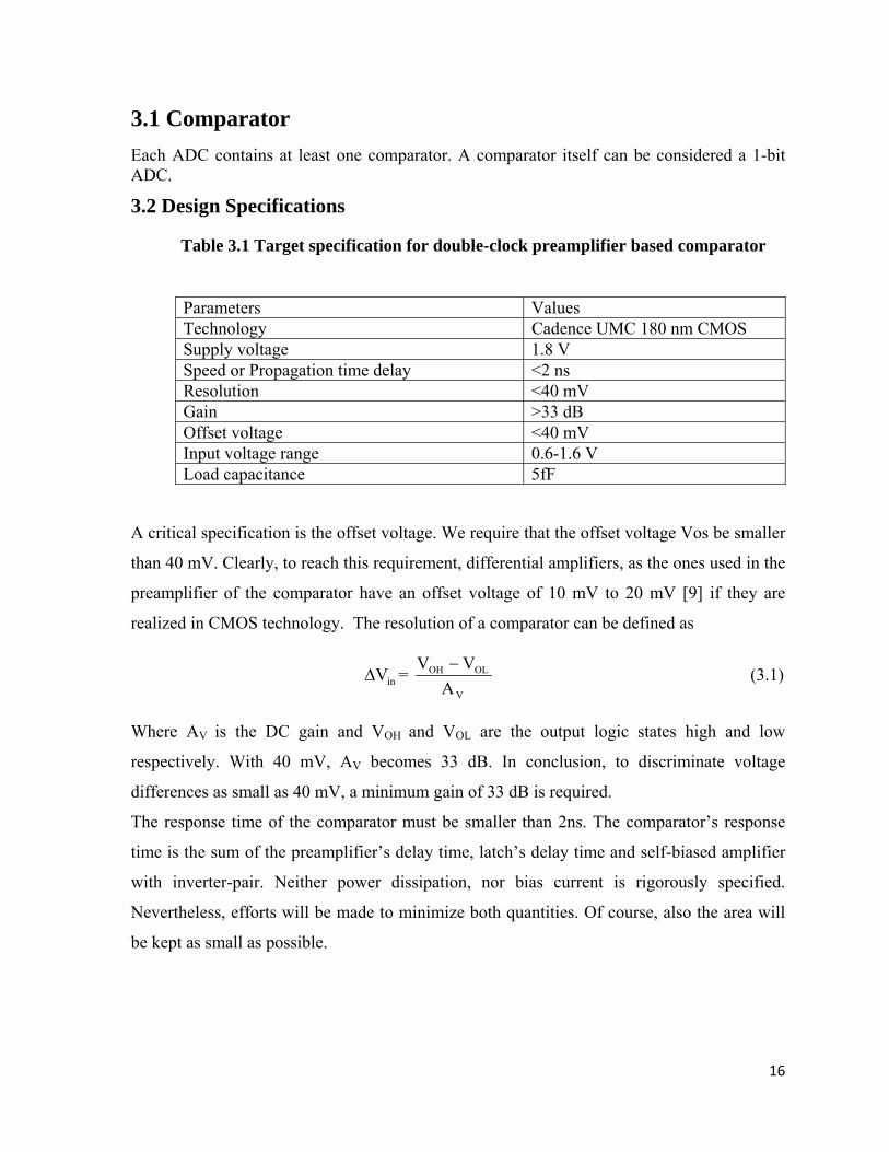
3.1 Comparator Each ADC contains at least one comparator. A comparator itself can be considered a 1-bit ADC.
3.2 Design Specifications
Table 3.1 Target specification for double-clock preamplifier based comparator
Parameters Values Technology Cadence UMC 180 nm CMOS Supply voltage 1.8 V Speed or Propagation time delay <2 ns Resolution <40 mV Gain >33 dB Offset voltage <40 mV Input voltage range 0.6-1.6 V Load capacitance 5fF
A critical specification is the offset voltage. We require that the offset voltage Vos be smaller
than 40 mV. Clearly, to reach this requirement, differential amplifiers, as the ones used in the
preamplifier of the comparator have an offset voltage of 10 mV to 20 mV [9] if they are
realized in CMOS technology. The resolution of a comparator can be defined as
inVΔ = V
OLOH
AVV −
(3.1)
Where AV is the DC gain and VOH and VOL are the output logic states high and low
respectively. With 40 mV, AV becomes 33 dB. In conclusion, to discriminate voltage
differences as small as 40 mV, a minimum gain of 33 dB is required.
The response time of the comparator must be smaller than 2ns. The comparator’s response
time is the sum of the preamplifier’s delay time, latch’s delay time and self-biased amplifier
with inverter-pair. Neither power dissipation, nor bias current is rigorously specified.
Nevertheless, efforts will be made to minimize both quantities. Of course, also the area will
be kept as small as possible.

17
3.2.1 Preamplifier The main design criteria’s for preamplifier are gain and bandwidth (cut-off frequency f-3dB).
If the preamplifier gain is AV=3=9.54 dB and f-3dB frequency is 600 MHz. The gain-
bandwidth product fGBW can be increased by increasing the bias current. However, low
power consumption is preferable. A bias current of 50μA is chosen.
Figure 3.2: Schematic of the preamplifier [14].
| VA | =3m
1m
gg
= 4m
2m
gg
(3.2)
dB3f − = |A|
f
V
GBW
(3.3)
mg = DILWkp2
(3.4)
Where gm is transconductance and kp is process transconductance.

18
3.2.2 Decision Circuit or Latch
Preamplifier amplified a minimum signal to a value much higher than the offset voltage of
the latch. The amplified signal (output of preamplifier) is applied to the latch through
transistors M5and M6 which provide isolation between the latch output and the inputs to the
preamplifier. Rapid changes in the output of the latch can propagate through the drain-gate
capacitances of the M1 and M2 that leads to the kick-back noise. It is important to remember
that ∆VO (the difference between the latch output voltages VO+ and VO- before the latch is
enabled) will always be less than VOH - VOL. So, the argument of the logarithm is always
greater than unity. There are several important observations to be made to decrease the
propagation time delay of the latch. The first is that the time required for outputs after
enabling the latch to reach VOH - VOL is decreased by applying a larger input to the latch,
∆VO, before enabling the latch. The second and more obvious is that the smaller the latch
time constant, the faster the response. If the input to the latch before enabling the latch, ∆VO,
is small, the latch takes a long time for the output voltages after enabling the latch to reach
VOH - VOL. Therefore, it is desirable to apply a reasonably large value of ∆VO in order to take
advantage of the rapidly increasing slope of the positive exponential characteristics of the
latch but there is a compromise between gain and bandwidth of the preamplifier [10].
Figure 3.3: Schematic of the latch [11], [12].

19
The propagation time delay of a latch can be found by:
pt =O
OLOHL V2
)VV(ln
Δ−
τ (3.5)
Where Lτ = D
3
ox Ikp2LWC67.0 is the latch time constant and COX is the gate capacitance per
unit area.
3.2.3 Output Buffer
As already mentioned, the main purpose of the output buffer is to convert the output of the
decision circuit into a logic signal (i.e., 0 or 1.8 V). The output buffer should accept a
differential input signal. The overall comparator gain is the product of the gain of the
preamplifier and the gain of the latch. The gain of inverters inserted after the latch does not
contribute to the overall gain anymore, as the latch already establishes full logic levels at VOH
and VOL. Nevertheless, additional inverters (called buffers or drivers) are used to drive the
capacitive load. The complete comparator circuit is given in Figure 3.4.
Preamplifier latch Self-biased amplifier with inverter-pair
Figure 3.4: Schematic of double-clock preamplifier based comparator [11].

20
The comparator circuit in Figure 3.4 works as follows: During nclk, the switches M11 and
M12 disconnect VO++ and VO-- from the sensing nodes (VO+ and VO-) and pulled up to VDD
by M14 and M15. When M13 is closed it equalizing the sensing node voltages. A mismatch
between the two differential input voltages causes an unequal amount of current to be
injected into the sensing nodes. When switch M13 is released, the first regeneration phase
starts, and the small current imbalance cause the cross coupled transistors M9 and M10 to pull
down one of the sensing nodes. Then M11 and M12 are opened, and either VO++ or VO-- is
pulled to ground, switching the state of the self-biased differential amplifier. The two non-
overlapping clocks are used to controlling the comparator operation [11].
Trade-offs exist for the switch sizing: making M11 and M12 large helps pulling down
the active branch quickly, but increases the glitch size when switching on. The size of the
transistors has to be kept small enough to prevent the glitches from feeding through the self-
biased differential amplifier to the comparator output. The size of the nclk switch can be kept
small, reducing parasitic capacitance on the regeneration nodes, and increasing the gain during
the sensing phase (end of nclk) because the current difference flowing through M13 causes a
larger voltage imbalance of the sensing nodes.
3.2.4 Simulation Results
In this section, the comparator that was discussed in the previous section will be analyzed
for their offset voltage, gain, propagation time delay, power dissipation using Cadence
Spectre and Virtuoso® Analog Design Environment simulation. All the parameters of the
double-clock preamplifier based comparator at the schematic level are shown below.
3.2.4.1 DC Analysis
For calculating DC analysis, both inputs Vin- and Vin+ are taken as the DC voltage
source. An important parameter of a comparator is its offset voltage. Offset voltage of the
comparator was measured by taking the value of input, Vin-, at 900 mV and the input, Vin+, of
the comparator swept from 0 V to 1.8. The temperature is 27◦C. From the Figure 3.5, we
can see that the systematic offset voltage is approximately 18 mV.

21
Figure 3.5: Test setup of comparator for DC response.
Figure 3.6: DC characteristics of the comparator of Figure 3.4.
If we take the derivative of the transfer curve, the gain of the comparator and thus the
smallest difference between (resolution) that can be discriminated between Vin+ and Vin-
become known. Figure 3.7 shows the gain of the comparator at about 50 (33.98 dB) so that
approximately 40 mV is needed to make the comparator output change logic levels.

22
Figure 3.7(a): Comparator gain as a function of input voltage.
Figure 3.7(b): Comparator gain (in dB) as a function of input voltage.

23
Figure 3.8: Resolution of the double-clock preamplifier based comparator. As shown in the above Figure, the minimum input voltage required for the comparator to
change its states is 0.1mV.
3.2.4.2 AC Analysis
For calculating AC analysis, , the input , Vin+ is a AC voltage source and Vin- is taken
as the DC voltage source. Using AC analysis, we find the preamplifier gain and
bandwidth.
Figure 3.9: Test setup of comparator for AC response.

24
Figure 3.10: AC response of the comparator.
Obtained gain and bandwidth of the preamplifier is 9.941 dB and 600.8 MHz respectively. 3.2.4.3 Transient Analysis
For observing the transient response of comparator a AC voltage source of 40mV and
250MHz is applied to the input, Vin+ , and the Vin- was set to 900 mV. We are driving the
Vin+ input of the comparator 40 mV over the Vin- . The transient response of comparator is
shown in figure 3.11.
Figure 3.11: The transient response of comparator.

25
The propagation time delay obtained from the above Figure 3.10 is 1.61485 ns including all
the three stages.
Preamplifier = 0.28805 ns
Latch= 1.02993 ns
Self-biased amplifier with inverter-pair= 0.29687 ns
3.2.4.4 Power Measurement
Figure 3.12: Measurement of power of the comparator.
Average power dissipation = 175 µW.

26
3.3 Design Specifications
Table 3.2 Target specification for single-clock preamplifier based comparator
Parameters Values Technology Cadence UMC 180 nm CMOS Supply voltage 1.8 V Speed or Propagation time delay <500ps Resolution <40 mV Gain >33 dB Offset voltage <40 mV Input voltage range 0.6-1.6 V Load capacitance 5fF
In this design all the specifications are remains same, only propagation time delay is
decreased from 2 ns to 500 ps.
3.3.1 Preamplifier There are several problems with the preamplifier of Figure 3.2. One is that the gain is very
small even for large differences of W / L values [3]. To achieve a higher gain (W / L) p must
decrease, thereby increasing |VGS -VTHP | and lowering the common mode level at the output
nodes. Figure 3.13 is used in order to alleviate the above difficulty but at the cost of extra
supply voltage [1].
Figure 3.13: preamplifier [1].

27
The problem of extra power supply is solved by the cross-coupled load. The load devices are
connected such that in differential mode, the outer transistors act as positive resistors, while
the cross-coupled devices act as negative resistors [13]. The negative resistance cancels the
positive, thus presenting high differential output impedance. An advantage of cross-coupling
is that the PMOS load provides implicit local common-mode feedback with no extra devices.
Therefore, the common-mode voltage is stabilized. The idea is to lower the gm of the load
devices by reducing their current rather than their aspect ratio.
Figure 3.14: Improved preamplifier [14].
Transistors M5and M6 are used to increase the current in MI and M2 so that the gain is
enhanced by the square root of the difference of currents in M1 and M2 to the current in M3
and M4 [3], [14]. This can be illustrated as follows.
| VA | =3m
1m
gg
=3
5
II
1 + (3.6)
If I5 is greater than I3, the gain can be enhanced by the square root of 1 plus the ratio of I5 to
13. If 15 = 313, the gain is boosted by a factor of 2.

28
The sizes of Ml and M2 are set by considering the diff-amp transconductance and the
input capacitance. The transconductance sets the gain of the stage, while the size of Ml
and M2 determines the input capacitance of the comparator [3].
3.3.2 Decision Circuit The positive feedback latch stage is used to determine which of the input signals is
larger and extremely amplifies their difference. Transistor M13 is controlled by the clock
switching; M9, M10, M11and M12 constitute a positive feedback unit. When the clock signal
Clk is high, a relatively state of the comparator to compare the results directly from the
preamplifier output decision [14]. When the clock signal Clk is low, M13 transistor cut-off,
and can effectively latch output signal, comparing this time to stop comparing, in the latch
state. It takes positive feedback from the cross gate connection of M9 and M10.
Consider i+ >> i- so that M11 and M10 are ON and M9 and M12 are OFF. Here also β11=
β12=βa and β9= β10=βb for which VO- is ~ 0V and VO+ is
+OV = THNVai2
+β
+ (3.7)
Where β =LWkp
Figure 3.15: Decision circuit [14].

29
If we start to increase i- and decrease i+, when drain to source voltage of M10 is equal
to the threshold voltage, VTHN of M9, switching takes place. At this point M9 takes
current away from M11 which decreases drain to source voltage of M11 and M10
turns off. If we assume that maximum value of VO+ or VO- is equal to 2VTHN, then
under these circumstances M9 and M10 operate under cut-off or triode region under
steady state conditions. Then voltage across M10 becomes VTHN and M10 enters into
saturation and current of M10 is
−i = +ββ
iab (3.8)
This is the point at which switching takes place; i.e. M10 shuts off and M9 turns on.
If βa= β, then switching takes place when the currents, i+ and i-, are equal. A
similar analysis of increasing i+ and decreasing i- results in
+i = −ββ
iab
(3.9)
The complete comparator circuit is given in Figure 3.16
Preamplifier Latch Self-biased amplifier with inverter-pair
Figure 3.16 Schematic of the single-clock preamplifier based comparator [14].

30
3.3.3 Simulation Results
3.3.3.1 DC Analysis
During DC analysis of this comparator, same input parameters are applied as for double-clock preamplifier based comparator. Offset voltage obtained is approximately 18 mV.
Figure 3.17: Offset voltage of the comparator.
Figure 3.18: Gain of the comparator.

31
Figure 3.19: Gain (in dB) of the comparator.
Gain of the comparator obtained from the derivative of the curve in Figure 3.16 and then convert to dB is 33.98 dB.
Figure 3.20: Resolution of the comparator.
The resolving capability of this comparator is 36 mV.

32
3.3.3.2 AC Analysis
During AC analysis of this comparator, same input parameters are applied as given in test setup for double-clock preamplifier based comparator.
Figure 3.21: AC analysis of the preamplifier stage of the single-clock comparator.
The gain and bandwidth of the preamplifier is 11.452 dB and 2.011 GHz respectively.
3.3.3.3Transient analysis
Figure 3.22: Transient response of the comparator.

33
Preamplifier’s delay= 0.10425 ns
Latch’s delay = 0.0142 ns
Self-biased amplifier with inverter-pair’s delay= 0.567265 ns
Total propagation time delay is 0.685715 ns.
3.3.3.4 Power Measurement
Figure 3.23: Power measurement of the comparator.
Average power dissipation =432.27 µW.

34
3.3.4 Process Corner Simulation Results
The following is the table of corners for the simulation of comparators.
Table 3.3: Corners simulation table.
Corners VDD Temperature TT 1.8 V 27°C SS 1.62 V 80°C FF 1.98 V -20°C SF 1.8 V 27°C FS 1.8 V 27°C
3.3.4.1 Pre-layout Simulation Results of the Double-clock Preamplifier
Based Comparator.
Table 3.4: Pre-layout simulation with process corner variations.
Table 3.5: Pre-layout Simulation with Temperature and VDD Variations.
Parameters TT SS FF SF FS Propagation time delay (ns)
1.6148 1.8066 1.4216 1.7175 1.4871
Offset(mV) 18 20 16.3 18 49 Gain(dB) 33.98 33.06 33.58 33.98 25.67 Power (µW) 175 155 256 114.3 259.7
Parameters TT SS FF SF FS Propagation time delay (ns)
1.6148 1.8747 1.3929 1.7162 1.4442
Offset (mV)
18 18 20 18 49
Gain (dB) 33.98 33.98 30.41 33.98 25.67 Power (µW)
175 76.51 370.20 116.56 261.25

35
3.3.4.2 Pre-layout Simulation Results of the Single-clock Preamplifier
Based Comparator.
Table 3.6: Pre-layout simulation with process corner variations.
Table 3.7: Pre-layout Simulation with Temperature and VDD Variations.
Parameters TT SS SF Propagation time delay (ns)
0.6857 0.8715 0.5264
Offset(mV) 18 18 18 Gain(dB) 33.98 33.06 33.98 Power (µW) 432.27 241.26 307.3
Comparators work better at all the corners as we can see from the above tables except FF and FS corner simulation of the single-clock preamplifier comparator. It may be due to the high current that leads to change of operation region or change of node voltages.
Parameters TT SS SF Propagation time delay (ns)
0.6857 0.8383 0.5358
Offset(mV) 18 18 18 Gain(dB) 33.98 33.98 33.98 Power (µW) 432.27 233.20 317.54

36
CHAPTER
4 LAYOUT DESIGN AND POST
LAYOUT SIMULATION
Introduction
In comparators, it is assumed that the circuits are perfectly symmetric i.e. two sides exhibit
identical properties and bias currents. But in reality identical devices suffers from a finite
mismatch due to uncertainties in each step of the manufacturing process. These mismatch
results in offset in the comparator. Multi-finger transistors use to reduce mismatch S/D
junction area and the gate resistance. Thumb rule for fingering is “the width of each finger is
chosen such that the resistance of the finger is less than the inverse transconductance
associated with the finger” [1]. Cadence Virtuoso® XL Layout Editing Software is used for
the layout design and DRC, LVS and RCX have been performed by using Cadence assura.
4.1 Layout of Double-clock Preamplifier Based Comparator.
Figure 4.1: Layout for double-clock preamplifier based comparator.

37
Figure 4.2: Layout Vs Schematic match.
Figure 4.3: RCX extracted view.

38
4.2 Layout of Single-clock Preamplifier Based Comparator.
Figure 4.4: Layout for single-clock preamplifier based comparator without multi-figure
technique.
Figure 4.5: Layout Vs Schematic match.

39
Figure 4.6: RCX extracted view.
4.2.1 Layout for Single-clock Preamplifier Based Comparator.
Figure 4.7: Layout for single-clock preamplifier based comparator with multi-figure
technique.

40
Figure 4.8: Layout Vs Schematic match.
Figure 4.9: RCX extracted view.

41
4.3 Post-Layout Simulation Results
4.3.1 Post-Layout Simulation Results of the Double-clock Preamplifier
Based Comparator.
Table 4.1: Post-layout simulation with process corners variations.
Parameters TT SS FF SF FS
Propagation
time delay
(ns)
1.6796 1.9599 1.4968 1.7647 1.5174
Offset(mV) 18 18 18 18 54
Gain(dB) 33.98 33.98 33.58 33.98 30.41
Power (µW) 185.11 87.72 383.48 124.29 270.34
4.3.2 Post-Layout Simulation Results of the Single-clock Preamplifier
Based Comparator.
Table 4.2: Post-layout simulation with process corners variations.
Parameters TT SS SF
Propagation time delay
(ns)
0.7475 0.9120 0.5226
Offset(mV) 18 18 18
Gain(dB) 33.98 33.98 33.98
Power (µW) 432.27 233.20 317.54
There is a slight change in the values of the parameters in the post-layout simulation of the
comparators due to the parasitic capacitance and resistance formation during the layout
design

42
CHAPTER
5 CONCLUSION AND FUTURE SCOPE OF WORK
5.1 Conclusion
In this thesis, the comparator circuits for high-speed ADCs have been investigated. The
designs are mainly optimized for the low propagation time, minimal input resolution and
minimal circuit area. Two comparator topologies, namely, double-clock preamplifier based
comparator and single-clock preamplifier based comparator have been analyzed and
designed. Both of the designs have been simulated with UMC 180nm CMOS technology.
The minimal propagation time delay of 2 ns, offset voltage of 18mV, resolution of 0.1mV
and power dissipation of 175 µW is achieved by the double-clock preamplifier based
comparator. The input signal frequency is half of the sampling frequency.
The minimal propagation time delay of 0.685 ns, offset voltage of 18mV, resolution of 36
mV and power dissipation of 432.27 µW is achieved by the double-clock preamplifier based
comparator. The input frequency is one eighth of the sampling frequency.
5.2 Future Scope of Work Simulation results show that both comparator give low offset voltage of 18mV. By using
Auto zeroing technique the offset voltage can be reduced further. The power dissipation of
double-clock preamplifier based comparator is 175 µW and for single-clock preamplifier
based comparator is 432.27 µW. By adding a MOSFET switch in series with the preamplifier
current source can significantly reduce static power dissipation of the preamplifier.

43
REFERENCES
[1] Behzad Razavi, “Design of Analog CMOS Integrated Circuits,” Tata McGraw-Hill, Inc.,
2002.
[2] HeungJun Jeon Yong-Bin Kim, “A CMOS Low-power Low-offset and High-speed Fully
Dynamic Latched Comparator,” IEEE International SOC Conference, pp. 285, September
2010.
[3] Philip E. Allen and Douglas R. Holberg, “CMOS Analog Circuit Design,” 2nd Edition,
Oxford University Press, First Indian Edition, 2010.
[4] R. Jacob Baker, Harry W. Li, David E. Boyce, “CMOS Circuit Design, Layout, and
Simulation,” 2nd Edition, IEEE Press Series on Microelectronic Systems, John Wiley &
Sons, Inc., 2002.
[5] R. Jacob Baker, Harry W. Li, David E. Boyce, “CMOS Circuit Design, Layout, and
Simulation,” 3rd Edition, IEEE Press Series on Microelectronic Systems, John Wiley &
Sons, Inc., 2010.
[6] Roubik Gregorian, “Introduction to CMOS Op-Amps and Comparators,” John Wiley &
Sons, Inc., 1999.
[7] Marcel J.M. Pelgrom, “Analog to Digital Converter,” Springer Edition, 2010.
[8] Bazes, M., “Two Novel Fully Complementary Self-biased CMOS Differential Amplifiers,”
IEEE Journal of Solid-State Circuits, Vol. 26, No.2, pp. 165, February 1991.
[9] N. Stefanou, Sameer R. Sonkusale, “An Average Low Offset Comparator for 1.25 GS/s ADC
in 0.18μm CMOS,” IEEE International Conference on Electronics, Circuits and Systems, pp.
246, December 2004.
[10] Bao-ni Han Yin-tang Yang Zhang-ming Zhu, “A Novel 1.25 GS/s Ultra High-speed
Comparator in 0.18μm CMOS,” IEEE International Conference on Solid-State and
Integrated-Circuit Technology, pp. 1957, October 2008.
[11] G. M. Yin, F. Op’t Eynde, and W. Sansen, “A High-Speed CMOS Comparator with 8-Bit
Resolution,” IEEE Journal of Solid-State Circuits, Vol. 27, pp. 208 - 211, February 1992.

44
[12] Meena Panchore and R. S. Gamad, “Low-power and High-speed CMOS Comparator Design
Using 0.18μm Technology,” International Journal of Electronic Engineering Research, Vol.
2, No. 1, pp. 71–77, June 2010.
[13] Bult, K. Buchwald, A., “An Embedded 240mW 10-Bit 50 MS/s CMOS ADC in 1mm2,”
IEEE Journal of Solid-State Circuits, Vol. 32, No.12, pp. 1887, October 1997.
[14] Jian-feng Wang Ji-hai Duan, “Design of an Ultra High-speed Voltage Comparator,” IEEE
Pacific Asia Conference on Circuits, Communications and System, Vol. 2, pp. 145, August
2010.