Studies on YBa2NbO6 and YBa2Cu3-xNbxOy Buffer Layers
56
Wright State University CORE Scholar Mechanical and Materials Engineering Faculty Publications Mechanical and Materials Engineering 4-2004 Studies on YBa2NbO6 and YBa2Cu3-xNbxOy Buffer Layers S. Sathiraju R. Wheeler Paul N. Barnes T. L. Peterson Iman Maartense See next page for additional authors Follow this and additional works at: hps://corescholar.libraries.wright.edu/mme Part of the Materials Science and Engineering Commons , and the Mechanical Engineering Commons is Conference Proceeding is brought to you for free and open access by the Mechanical and Materials Engineering at CORE Scholar. It has been accepted for inclusion in Mechanical and Materials Engineering Faculty Publications by an authorized administrator of CORE Scholar. For more information, please contact [email protected], [email protected]. Repository Citation Sathiraju, S., Wheeler, R., Barnes, P. N., Peterson, T. L., Maartense, I., Campbell, A. L., Yust, N. A., Haugan, T. J., Jia, Q., Arendt, P., Mukhopadhyay, S. M., & Vemulakonda, S. (2004). Studies on YBa2NbO6 and YBa2Cu3-xNbxOy Buffer Layers. Proceedings of AFOSR HTS Coated Conductor. hps://corescholar.libraries.wright.edu/mme/62
Transcript of Studies on YBa2NbO6 and YBa2Cu3-xNbxOy Buffer Layers

Wright State UniversityCORE ScholarMechanical and Materials Engineering FacultyPublications Mechanical and Materials Engineering
4-2004
Studies on YBa2NbO6 and YBa2Cu3-xNbxOyBuffer LayersS. Sathiraju
R. Wheeler
Paul N. Barnes
T. L. Peterson
Iman Maartense
See next page for additional authors
Follow this and additional works at: https://corescholar.libraries.wright.edu/mme
Part of the Materials Science and Engineering Commons, and the Mechanical EngineeringCommons
This Conference Proceeding is brought to you for free and open access by the Mechanical and Materials Engineering at CORE Scholar. It has beenaccepted for inclusion in Mechanical and Materials Engineering Faculty Publications by an authorized administrator of CORE Scholar. For moreinformation, please contact [email protected], [email protected].
Repository CitationSathiraju, S., Wheeler, R., Barnes, P. N., Peterson, T. L., Maartense, I., Campbell, A. L., Yust, N. A., Haugan, T. J., Jia, Q., Arendt, P.,Mukhopadhyay, S. M., & Vemulakonda, S. (2004). Studies on YBa2NbO6 and YBa2Cu3-xNbxOy Buffer Layers. Proceedings of AFOSRHTS Coated Conductor.https://corescholar.libraries.wright.edu/mme/62

AuthorsS. Sathiraju, R. Wheeler, Paul N. Barnes, T. L. Peterson, Iman Maartense, A. L. Campbell, N. A. Yust, T. J.Haugan, Q. Jia, Paul Arendt, Sharmila M. Mukhopadhyay, and S. Vemulakonda
This conference proceeding is available at CORE Scholar: https://corescholar.libraries.wright.edu/mme/62

AFRL-PR-WP-TR-2006-2076
SCIENTIFIC PRESENTATIONS ON
SUPERCONDUCTIVITY FROM 2002-2005 Paul N. Barnes and Lt. Brandon Craig Harrison
Power Generation Branch (AFRL/PRPG)
Power Division
JANUARY 2006
Final Report
Approved for public release; distribution unlimited.
See additional restrictions described on inside pages
STINFO COPY
AIR FORCE RESEARCH LABORATORY
PROPULSION DIRECTORATE
WRIGHT-PATTERSON AIR FORCE BASE, OH 45433-7251
AIR FORCE MATERIEL COMMAND
UNITED STATES AIR FORCE

NOTICE Using Government drawings, specifications, or other data included in this document for any purpose other than Government procurement does not in any way obligate the U.S. Government. The fact that the Government formulated or supplied the drawings, specifications, or other data does not license the holder or any other person or corporation; or convey any rights or permission to manufacture, use, or sell any patented invention that may relate to them. This report was cleared for public release by the Air Force Research Laboratory Wright Site (AFRL/WS) Public Affairs Office (PAO) and is releasable to the National Technical Information Service (NTIS). It will be available to the general public, including foreign nationals. PAO Case Number: AFRL/WS-06-0325, 07 Feb 2006 THIS TECHNICAL REPORT IS APPROVED FOR PUBLICATION. /s/ /s/ ____________________________________ _____________________________________ BRANDON C. HARRISON 2d Lt, USAF C. SCOTT RUBERTUS Research Chemist Branch Chief Power Division, AFRL/PRPG Power Division, AFRL/PRPG /s/ ____________________________________ RICHARD FINGERS Deputy for Technology Power Division, AFRL/PRP This report is published in the interest of scientific and technical information exchange and its publication does not constitute the Government’s approval or disapproval of its ideas or findings.

REPORT DOCUMENTATION PAGE Form Approved
OMB No. 0704-0188
The public reporting burden for this collection of information is estimated to average 1 hour per response, including the time for reviewing instructions, searching existing data sources, gathering and maintaining the data needed, and completing and reviewing the collection of information. Send comments regarding this burden estimate or any other aspect of this collection of information, including suggestions for reducing this burden, to Department of Defense, Washington Headquarters Services, Directorate for Information Operations and Reports (0704-0188), 1215 Jefferson Davis Highway, Suite 1204, Arlington, VA 22202-4302. Respondents should be aware that notwithstanding any other provision of law, no person shall be subject to any penalty for failing to comply with a collection of information if it does not display a currently valid OMB control number. PLEASE DO NOT RETURN YOUR FORM TO THE ABOVE ADDRESS.
1. REPORT DATE (DD-MM-YY) 2. REPORT TYPE 3. DATES COVERED (From - To)
January 2006 Final 01 January 2001 – 31 October 2005
4. TITLE AND SUBTITLE
SCIENTIFIC PRESENTATIONS ON SUPERCONDUCTIVITY FROM 2002-2005
5a. CONTRACT NUMBER
In-house
5b. GRANT NUMBER
5c. PROGRAM ELEMENT NUMBER
62203F
6. AUTHOR(S)
Paul N. Barnes and Lt. Brandon Craig Harrison
5d. PROJECT NUMBER
3145 5e. TASK NUMBER
32
5f. WORK UNIT NUMBER
314532Z9
7. PERFORMING ORGANIZATION NAME(S) AND ADDRESS(ES) 8. PERFORMING ORGANIZATION
Power Generation Branch (AFRL/PRPG)
Power Division
Air Force Research Laboratory, Propulsion Directorate
Wright-Patterson Air Force Base, OH 45433-7251
Air Force Materiel Command, United States Air Force
REPORT NUMBER
AFRL-PR-WP-TR-2006-2076
9. SPONSORING/MONITORING AGENCY NAME(S) AND ADDRESS(ES) 10. SPONSORING/MONITORING
Air Force Research Laboratory
Propulsion Directorate
Wright-Patterson Air Force Base, OH 45433-7251
Air Force Materiel Command
United States Air Force
AGENCY ACRONYM(S)
AFRL/PRPG
11. SPONSORING/MONITORING AGENCY REPORT NUMBER(S)
AFRL-PR-WP-TR-2006-2076
12. DISTRIBUTION/AVAILABILITY STATEMENT
Approved for public release; distribution unlimited.
13. SUPPLEMENTARY NOTES
PAO Case Number: AFRL/WS-06-0325; Clearance Date: 07 Feb 2006. Document contains color.
14. ABSTRACT
This program addresses the basic scientific and engineering issues related to the development of the second-generation
high- temperature superconducting (HTS) coated conductor for use in magnet and generator coil windings of power
applications relevant to the Air Force (AF).
Current work focuses on the development of an ac YBCO-coated conductor and enhancement of the current dc coated
conductor. The dc coated conductor development is done as part of an overall AF program that includes industry and
academic research facilities. This program is coordinated with the Department of Energy’s Coated Conductor Program to
ensure integration with no redundancy. Flux pinning in the conductor is a significant focus of the overall coated conductor
work to improve in-field critical currents. The ac loss issues as well as stability (and quench protection) ultimately must be
considered for study, and work has commenced in this area within the in-house program. In order for the conductor to be
ready for projected power generation requirements (for directed energy weapons), the superconductivity group is
determining the unique AF requirements of the conductor and investigating ac loss and flux pinning issues.
15. SUBJECT TERMS
YBCO, superconductor, coated conductor, flux pinning, nanoparticles, thin films, high critical current, ac loss, MOD,
MOCVD
16. SECURITY CLASSIFICATION OF: 17. LIMITATION OF ABSTRACT:
SAR
18. NUMBER OF PAGES
416
19a. NAME OF RESPONSIBLE PERSON (Monitor)
a. REPORT
Unclassified
b. ABSTRACT
Unclassified
c. THIS PAGE
Unclassified
2d Lt Brandon Craig Harrison 19b. TELEPHONE NUMBER (Include Area Code)
N/A
Standard Form 298 (Rev. 8-98) Prescribed by ANSI Std. Z39-18

333 Approved for public release; distribution unlimited.
5.3 Studies on YBa2NbO6 and YBa2Cu3-xNbxOy Buffer Layers
References: 17, 36, 37, 38, 39
S.Sathiraju, R. Wheeler, P.N. Barnes, T.L.Peterson, I . Maartense, A.L.Campbell, R. M.
Nekkanti, L. Brunke, J.Murphy, T. A.Campbell, N. A. Yust, T. J. Haugan
Q. Jia and Paul Arendt
STC, Los Alamos National Laboratory, NM
S.Mukhopadya, S. Vemulakonda
Wright-State University, Dayton, OH
Presented at AFOSR REVIEW, January 19, 2004
Presented at ACERS 106 annual meeting, April 20, 2004
5.3.1 Objective
• YSZ, Y2O3 , LaMnO3 SrRuO3 etc are perovskite buffers
• LANL, ORNL, SNL, AFRL actively working on this.
• FUJIKURA, Japan - Gd2Zr2O7 Successful
• All buffers so far needs a CeO2 cap layer
• SNL has projected $1- $3 per KA-m using solution based methods by 2010
• However, the search is on for an ideal buffer layer…!
Figure 5.3.1.1

334 Approved for public release; distribution unlimited.
5.3.2 Present Work
• Ba2YNbO6 double perovskite
• 0.84 nm (Double the unit cell of MgO)
• No reaction up to 1200oC with Y123 or R-123 materials
• YBa2Cu3-xNbx Oy x = 0.25, 0.5 , 0.75 and 1.0
• ao ~ 0.4 nm
• Conducting as well as insulating buffers are possible
5.3.3 Experimental
Parameters YBa2Cu3-xNbxOy
x= 0.25,0.5,0.75,1
Ba2YNbO6 YBa2Cu3Oy
Deposition
Temp.
750 – 850 oC RT – 850
oC 750-820
o C
Oxygen
Pressure
250 mTorr 200 mTorr 230mTorr
Laser Energy 2.5 J/cm2 2 J/Cm
2 2 J/Cm
2
Laser frequency 4- 10 Hz 10 Hz 4-10Hz
S-T distance 6 cm 6 cm 6 cm
Substrates LAO, STO, MgO,
Rabits Ni, I- MgO
MgO, IBAD
MgO
All buffered
substrates
Thickness 200nm – 500nm 200 nm 200-500 nm
Figure 5.3.3.1
5.3.4 YBa2Cu3-xNbxOy films deposited at 750 oC
• Highly 00l oriented films were obtained for x = 0.25
• 00l oriented peaks started broadening
• Mixed phases were obtained for x = 1.0
• Those phases may be YBNO, Y123 or YBCNO?
• No CuO peak observed

335 Approved for public release; distribution unlimited.
Figure 5.3.4.1
5.3.5 YBa2Cu3-xNbxOy films deposited at 800 oC
• The h00 oriented peak intensities increased with the increase of substrate
temperature from 800 to 850 oC, and formation of single phase YBCNO was
observed in films
• No CuO peak observed
0
50000
100000
150000
200000
250000
20 25 30 35 40 45 50
2 Theta
Inte
nsit
y (
arb
)
YBCN
100
LAO
LAO
YBCN
200
YBCN
111
003 004 005
006
(a)(b)
(c)
(d)
(a) = 0.25
(b) = 0.5
(c) = 0.75
(d) = 1.0
YBCN

336 Approved for public release; distribution unlimited.
Figure 5.3.5.1
5.3.6 YBa2Cu3-xNbxOy films deposited at 850o C
• Using PrBa2Cu2NbO8 (PBCNO) PDF file (#43-0176) the peaks present in our
samples were indexed.
• The d values and peak positions are different from PBCNO compound.
• YBCNO may be tetragonal with lattice parameters a = 0.409nm and c = 1.16nm
0
20000
40000
60000
80000
100000
120000
140000
20 25 30 35 40 45 50
2 (°)
Inte
nsity (
arb
)
YBCNO
<200>
d)
c)
b) a)
YBCNO
<100>
LAO
LAO
<400> <500> <600>
LAO
a) x = 0.25
b) x = 0.5
c) x = 0.75
d) x = 1.0
<300> a)

337 Approved for public release; distribution unlimited.
Figure 5.3.6.1
5.3.7 YBa2Cu2NbOy films on various substrates
• No CuO peak was observed in films deposited on any of these substrates
• Highly oriented films were observed on STO and MgO
• 113 peak growth becoming strong with the increase of temperature above 825 oC
XRD of YBa2Cu(3-x)NbxO8 Films Deposited at 850°C
0
20000
40000
60000
80000
100000
120000
5 10 15 20 25 30 35 40 45 50 55
2 (°)
Inte
nsity (
arb)
x=0.25
x=0.5
x=0.75
x=1.0
<100> <200>

338 Approved for public release; distribution unlimited.
Figure 5.3.7.1
5.3.8 YBa2Cu2NbO8 on MgO deposited at 850 oC
Figure 5.3.8.1
0
2000
4000
6000
8000
10000
12000
20 25 30 35 40 45 50
2 Theta
Inte
ns
ity
(a
rb.
un
its
)
100
100
111/MgO
200
200
MgO
STO200
LAO
LAO
MgOMgO
111
a) STO
b) LAO
c) MgO
339 Approved for public release; distribution unlimited.
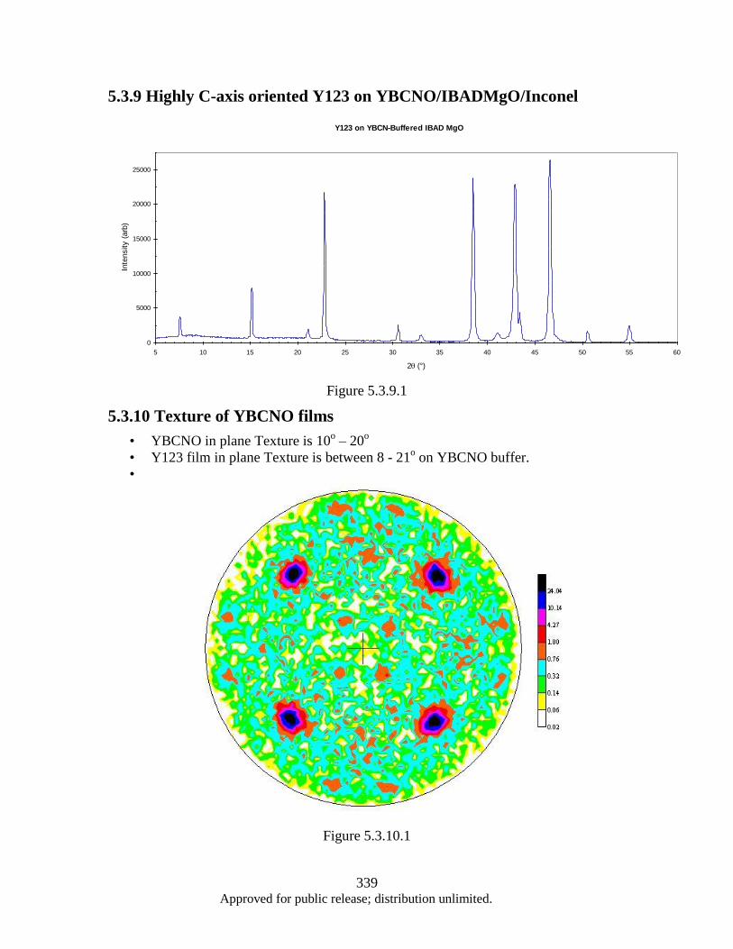
5.3.9 Highly C-axis oriented Y123 on YBCNO/IBADMgO/Inconel
Figure 5.3.9.1
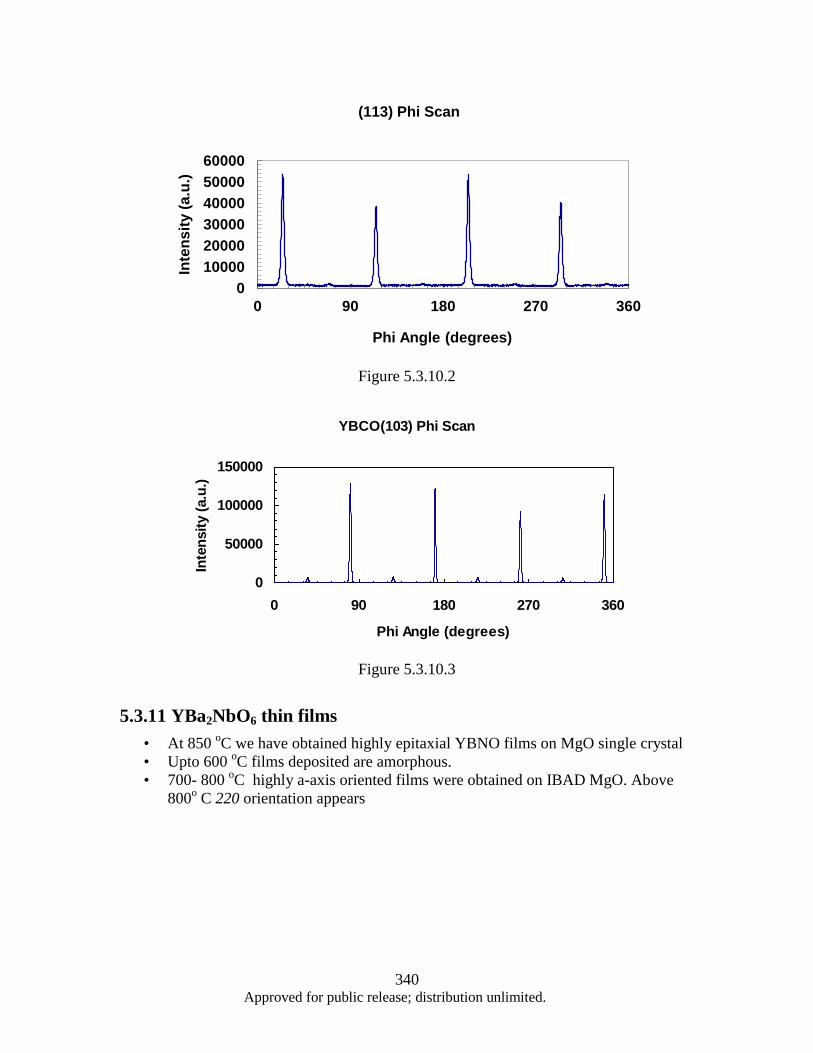
5.3.10 Texture of YBCNO films
• YBCNO in plane Texture is 10o – 20
o
• Y123 film in plane Texture is between 8 - 21o on YBCNO buffer.
•
Figure 5.3.10.1
Y123 on YBCN-Buffered IBAD MgO
0
5000
10000
15000
20000
25000
5 10 15 20 25 30 35 40 45 50 55 60
2 (°)
Inte
nsity (
arb
)
340 Approved for public release; distribution unlimited.
Figure 5.3.10.2
Figure 5.3.10.3
5.3.11 YBa2NbO6 thin films
• At 850 oC we have obtained highly epitaxial YBNO films on MgO single crystal
• Upto 600 oC films deposited are amorphous.
• 700- 800 oC highly a-axis oriented films were obtained on IBAD MgO. Above
800o C 220 orientation appears
0
10000
20000
30000
40000
50000
60000
0 90 180 270 360
Inte
ns
ity (
a.u
.)
Phi Angle (degrees)
(113) Phi Scan
YBCO(103) Phi Scan
0
50000
100000
150000
0 90 180 270 360
Phi Angle (degrees)
Inte
nsit
y (
a.u
.)

341 Approved for public release; distribution unlimited.
Figure 5.3.11.1
5.3.12 YBNO deposited on IBAD MgO/Inconel
Substrate FWHM of YBNO
220 peak
FWHM of YBCO
103 peak
MgO 8° 6°
IBADMgO/Inconel 6° 5°
Inconel 28° 21°
Figure 5.3.12.1
Figure 5.3.12.2
(220) Phi Scan
0
10000
20000
30000
40000
50000
60000
0 90 180 270 360
Phi Angle (degrees)
Inten
sit
y (
a.u
.)
YBNO on IBAD MgO
0
5000
10000
15000
20000
5 20 35 50
2 Theta (degrees)
In
ten
sity (a.u
.)
XRD of YBNO on MgO
0
10000
20000
10 25 40 55 70
2 Theta (degrees)
Inten
sit
y (
a.u
.)

342 Approved for public release; distribution unlimited.
5.3.13 AC Susceptability of Y123/YBCNO/INCONEL
Figure 5.3.13.1
Y 123 on YBCNO buffered STO
Figure 5.3.13.2
YBCNO (x =0.25) on LAO
Y-123 /YBCN/Inconel
-0.9
-0.8
-0.7
-0.6
-0.5
-0.4
-0.3
-0.2
-0.1
0
20 30 40 50 60 70 80 90 100
TEMPERATURE (K)
X'
0.025 Oe
0.1 Oe
0.25 Oe
0.5 Oe
1.0 Oe
1.5 Oe
2.2 Oe
-1
-0.9
-0.8
-0.7
-0.6
-0.5
-0.4
-0.3
-0.2
-0.1
0
82 84 86 88 90 92 94
X'
TEMPERATURE (K)
Y-123 on SrTiO3
0.025 Oe 0.1 Oe
0.25 Oe
0.5 Oe
1.0 Oe
1.5 Oe
2.2 Oe

343 Approved for public release; distribution unlimited.
Figure 5.3.13.4
5.3.14 Transport results of Y-123 films
Y123 films on Tc K Jc 77K MA
YBCNO/LAO 85 0.005
YBCNO/MgO 87 0.09
YBCNO/STO 90 0.8
YBCNO(0.25)/STO 87 0.5
YBNO/MgO 87 0.1
YBNO/IBADMgO 86 0.2
CeO2/YBNO/IMgO 87 0.5
YBNO/Inconel 85 0.001
Figure 5.3.14.1
Tc of YBCNO films and Y123 films deposited on these films
-1
-0.8
-0.6
-0.4
-0.2
0
75 80 85 90
X'
TEMPERATURE (K)
YBCNO (Nb = 0.25) on LAO
0.025 Oe 0.1 Oe
0.25 Oe
0.5 Oe
1.0 Oe
1.5 Oe
2.2 Oe

344 Approved for public release; distribution unlimited.
Figure 5.3.14.2
76
78
80
82
84
86
88
Nb0.25 Nb0.5 Nb0.75 Nb1
Buffer Layer
Tc (
K)
BLTs= 750
BL Ts= 800
BL Ts =850
0
10
20
30
40
50
60
70
80
90
100
0 0.25 0.5 0.75 1
X (Nb) concentration
Cri
tical T
em
pera
ture
(K
)
Ts = 750
Ts = 800
Ts = 850

345 Approved for public release; distribution unlimited.
5.3.15 AFM micrographs of YBa2Cu3-xNbxOy and analysis
Figure 5.3.15.1
Figure 5.3.15.2 Figure 5.3.15.3
Film Average Ra nm
X = 0.25 25
X = 0.5 46
X = 0.75 76
X = 1.0 120
YBCNO/Inconel 170
YBCNO/I-MgO 3
YBNO/MgO 6
YBNO/I-MgO 1.5
YBCNO/IBADMgO
YBNO/IBADMgO
0.25 0.5
0.75

346 Approved for public release; distribution unlimited.
5.3.16 XPS Studies of YBa2Cu3-xNbxOy (x = 0.25, 0.5, 0.75, 1) thin films
• A survey scan XPS spectrum was taken with binding energy varying from 0 to
1000 eV. It contains almost all the peaks from the elements present on the surface
• The surface was etched for 5 minutes using 3 KeV Ar+ ions, the amount of carbon
reduced to negligible amounts showing that the surface got cleaned up.
Figure 5.3.16.1

347 Approved for public release; distribution unlimited.
Figure 5.3.16.2
5.3.17 Cu-2p binding energy of YBCNO films
• Cu 2p binding energies does not corresponding to CuO
• Which confirms that Cu exists in +2 Valance state
• We expect that YBa2Cu2NbO8 phase forms in thin films

348 Approved for public release; distribution unlimited.
Figure 5.3.17.1
5.3.18 Raman Microscopy Studies
• 1 minute Raman spectra were collected on YBa2Cu3-xNbxO8 films.
• X= 0.25 retains ortho-rhombic nature and reflects in Raman orthorhombic modes
of Y123 150, 230, 330, 500 and 575cm-1
• Raman modes at 150, 230 and 500 cm-1
started dissolving slowly for x = 0.5 and
0.75
• For x =1.0 we have seen the complete absence of the orthorhombic peaks belong
to Y-123 film structure.
• Shift in 334 cm-1
to higher side (350cm-1
) and the Raman shift at 501 cm-1
is
completely absent for the film with x =1.0.
• No mode correspond to CuO has been observed.

349 Approved for public release; distribution unlimited.
Figure 5.3.18.1
• By studying the raman shifts on three different substrates and identified the
YBCNO modes
• Disappearance of peak at 500 cm -1
and decrease of 330 cm-1
mode clearly
indicates that an existence of pronounced cation disorder in 123 crystal structure
which confirms the transformation of orthorhombic phase to cubic phase
• YBa2NbO6 films are cubic and hence show no raman active mode.
• There is phase transformation from ortho to tetrogonal in YBCNO films
0
2000
4000
6000
8000
10000
12000
0 100 200 300 400 500 600
Raman Shift (cm-1
)
Inte
nsity (
arb
)
150
(A)
(B)
(C)
(D)
A) x = 0.25
B) x = 0.5
C) x = 0.75
D) x = 1.0
235
334
501

350 Approved for public release; distribution unlimited.
Figure 5.3.18.2
0
500
1000
1500
2000
2500
3000
3500
4000
4500
5000
0 200 400 600 800 1000 1200
RAMAN SPECTRA OF YBNO
FILM
Raman Spectra of YBa2Cu2NbO8 Films on Varying Substrates
0
5000
10000
15000
20000
0 100 200 300 400 500 600 700 800 900 1000
Raman Shift (cm-1)
Inte
nsity
(arb
)
LAO
STO
MgO

351 Approved for public release; distribution unlimited.
5.3.19 Cross sectional TEM of YBa2Cu2NbO8 film on STO deposited at
800 oC
Figure 5.3.19.3
TEM cross section prepared by
FIB
- Pt protective layer
- Cut with Ga ion beam and lift
out onto Cu grid bar
- Final thin with fine Ga beam
(30 kV)
SrTiO3
YBCNO Pt
YBNO
Dark Field
Figure 5.3.19.1
Figure 5.3.19.2

352 Approved for public release; distribution unlimited.
5.3.20 EDS SPECTRA OF YBCNO FILM
• It shows the Y and Nb Ka peaks with an intensity ratio of very nearly one.
• Excess Cu intensity is taken into account, the Ba L peak and Cu K peak intensity
ratio is very close to unity and indicates a ratio of Ba or Cu with Y of 2:1.
• These observations suggest film has a compositional stoichiometry of
approximately YBa2Cu2NbO8.
Figure 5.3.20.1
5.3.21 Stoichiometry of YBa2Cu2NbOy
Figure 5.3.21.1
N
b
B
a T
i
Y
Nb
Cu
Ba
Ti

353 Approved for public release; distribution unlimited.
5.3.22 TEM S.A.D Micrograph of YBa2Cu2NbOx
• Orientation images indicates that YBCNO film is epitaxial
• The pattern in this figure is oriented along the [001] axis of the cubic SrTiO3
substrate and contains strong {200} and {110} type reflections.
• The STO phase was used to calibrate the lattice parameter of the new phase which
has a0~0.41nm. While this electron diffraction pattern suggests that the YBa-
2Cu2NbOx phase has one 4-fold axis of symmetry.
Figure 5.3.22.1
5.3.23 Summary Notes
• Substrate Temperature and Nature plays critical role in the Phase formation of
YBCNO films
• At 800 oC we have observed highly a – axis oriented YBa2Cu2NbO8 films have
grown on STO substrate
• Around 850 oC single phase YBCNO has been observed in our studies.
• XPS, micro-raman results show no formation of CuO phase.
• TEM analysis has confirmed the growth of stoichiometric and highly a-axis
oriented YBa2Cu2NbO8 films.
• Raman Studies shows a systematic phase transformation in YBCNO films (from
orthorhombic to tetragonal)
• Y-123 Films deposited directly on YBCNO buffered Inconel are poor in quality.
• YBa2Cu2NbO8 Phase does forms on single crystal substrates and its a~ 0.41 and c
~ 1.18 nm.
• YBa2NbO6 a new double perovskite buffer with a~ 0. 84 nm appears to be
promising for coated conductor applications. Further studies are in progress.

354 Approved for public release; distribution unlimited.
5.4 Growth of oxide and metal buffer layers for coated conductor
applications
References: 17, 36, 37, 38, 39
Presented At
AFOSR REVIEW, January 24, 2005
SRINIVAS SATHIRAJU
National Research Council
Propulsion Directorate
Air Force Research Laboratory
5.4.1 BYNO films
WHY BYNO ?
• Ba2YNbO6 double perovskite
• 0.84 nm (Double the unit cell of MgO)
• No reaction up to 1200 oC with Y123 or R-123 materials
• Last year we have achieved only 0.5 MA/cm2 Jc at 77K on metallic substrates.
• 1MA/cm2 Jc on single crystal substrates
5.4.2 AC susceptibility results
Figure 5.4.2.1
Ag 5% Y123 on BYNO
-1
-0.8
-0.6
-0.4
-0.2
0
82 84 86 88 90 92 94
TEMPERATURE (K)
'0.025 Oe
0.1 Oe
0.25 Oe
0.5 Oe
1.0 Oe
1.5 Oe
2.2 Oe
5%Ag+Y123/BYNO (100nm)
X’

355 Approved for public release; distribution unlimited.
Y123/BYNO (200nm)
5.4.3 BYNO thickness variation on IMgO
THICKNESS
OF BYNO
(nm)
YBCO Tc (K) YBCO Jc
MA/cm2
@77K
Ag 5% YBCO
Tc (K)
Ag 5% YBCO
Jc (MA/cm2)
@77K
50 88 0.01
100 89 0.5 89 1.09
200 89 0.9 91 3.2
250 91 1.2
300 91 1.6
Figure 5.4.3.1
SS146
-1
-0.8
-0.6
-0.4
-0.2
0
82 84 86 88 90 92 94
TEMPERATURE (K)
'0.025 Oe
0.1 Oe
0.25 Oe
0.5 Oe
1.0 Oe
1.5 Oe
2.2 Oe

356 Approved for public release; distribution unlimited.
5.4.4 Texture Analysis from Sandia National Lab
Figure 5.4.4.1
5.4.5 Rocking curve of MgO
Figure 5.4.5.1
SNL1 MgO (220) omega scan
Omega (degrees)
20 25 30 35 40 45
Inte
nsity (
arb
itra
ry u
nits)
FWHM = 7.87 degrees
YBNO (200) YBNO (220)

357 Approved for public release; distribution unlimited.
5.4.6 BYNO(220) Phi-scan
Figure 5.4.6.1
5.4.7 Sample information and summary
• Sample -1, UA-1: BYNO on single crystal MgO substrate
• Sample-2, UA-2: BYNO on single crystal MgO substrate, different deposition
parameters
• Sample-3, UA-3: BYNO on metal substrate
• In sample-1 and -2, a thin layer of Au-Pd was deposited on the surface to prevent
charging during FIB cross sectioning
• RBS was performed at 3.8 MeV using 4He atoms
Sample Composition from
RBS
RBS thickness
(nm) ± 10
FIB thickness
(nm)
UA-1 YNbBa2O6 1100 608 ± 32
UA-2 YNbBa2O6 340 310 ± 25
UA-3 Y1.1Nb1.2Ba2O6 280 254 ± 10
Figure 5.4.7.1
Additional work is required to delineate the reason for discrepancy between the thickness
from RBS and FIB for sample-1
SNL1 YBNO (220) phi scan
Phi (degrees)
0 45 90 135 180 225 270 315 360
Inte
nsity (
arb
itra
ry u
nits)
FWHM ~ 7.7o

358 Approved for public release; distribution unlimited.
5.4.8 FIB cross section- tilted at 45o
Figure 5.4.8.1
Figure 5.4.8.2
50 kX
UA-2
1 μm
YNBO thickness: 310 ± 25 nm
Pt
BYNO MgO
1 μm
50 kX
UA-3
YNBO thickness: 254 ± 10 nm
Pt
BYNO
Hastelloy
IMgO

359 Approved for public release; distribution unlimited.
Figure 5.4.8.3
5.4.9 RBS Analysis of BYNO film
Figure 5.4.9.1
RBS spectrum at 3.8 MeV
0 500 1000 1500 2000
Channel
0
10
20
30
40
50
No
rmal
ized
Yie
ld
0 1 2 3
Energy (MeV)
B60526 UA1Simulation of Au-Pd/Nb-O-Y-Ba/O-Mg
Pt
BYNO
MgO
1 μm
50 kX
UA-1
YNBO thickness: 608 ± 32 nm

360 Approved for public release; distribution unlimited.
Figure 5.4.9.2
Peaks of Nb and Y are very close
Figure 5.4.9.3
0 500 1000 1500 2000
Channel
0
10
20
30
40
50
No
rmal
ized
Yie
ld
0 1 2 3
Energy (MeV)
B60529 UA3Simulation of Nb-O-Y-Ba/O-Mg/Ni
0 500 1000 1500 2000
Channel
0
10
20
30
40
50
No
rmal
ized
Yie
ld
0 1 2 3
Energy (MeV)
B60528 UA2Simulation of Au-Pd/Nb-O-Y-Ba/O-Mg

361 Approved for public release; distribution unlimited.
5.4.10 Cross sectional TEM Image of YBCO/BYNO/IMgO/Hastelloy
Figure 5.4.10.1
5.4.11 Ag and Ca doped YBCO films
• In order to over come the oxygen deficiency in the YBCO films we have used Ag
5 wt% doped YBCO films
• Ag doped films carried 2-4 MA/cm2 Jc at 77 K.
• Thickness of BYNO buffer is 100nm and YBCO is 300nm.
• Very well oxygenated YBCO films have carried 1 MA/cm2 Jc at 77K.
• Ca doped Y-123 also have 1-3 MA/Cm2 at 77K
5.4.12 Ba2YNbO6 film deposited on Textured Ni
• When deposited in vacuum we have seen oxidation of the substrate
• Reduced atmosphere we have improved the situation and highly a-axis oriented
BYNO films were obtained
• No formation of NiO but difficult to confirm through X-ray as 400 peak of
BYNO and NiO 100% peak 012 appears around 43o
Pt layer
200nm YBCO
Layer
BYNO 100nm
IBAD MgO 10nm
HASTELLOY

362 Approved for public release; distribution unlimited.
Figure 5.4.12.1
Figure 5.4.12.2
5.4.13 YBa2NbO6 films on RABiTS Cu-alloy
• Texturing of Cu –alloy : Attend Varanasi presentation for more details
• BYNO film deposited on textured Cu-alloy substrate shows strong 400 orientation
along with 220(40%) and 222 (6%) orientations when deposited at 780 oC
• However, there is no CuO peak
• When BYNO deposited at 850 oC 400 orientation dominated the process.
0
500
1000
1500
2000
2500
20 22 24 26 28 30 32 34 36 38 40 42 44 46 48 50
2 Theta (o)
Inte
nsit
y (
arb
.un
its)
200
220
222
400
YBNO
BYNO deposited at 800 oC

363 Approved for public release; distribution unlimited.
Figure 5.4.13.1
5.4.14 Micro-Raman Studies of YBNO films
• YBa2NbO6 films are cubic and hence show no raman active mode.
• There is no Raman mode of NiO observed
• There is no Raman active mode corresponding to CuO in YBNO films on Cu-
alloy substrate
0
200
400
600
800
1000
1200
1400
1600
1800
2000
20 22 24 26 28 30 32 34 36 38 40 42 44 46 48 50
2 Theta (o)
Inte
nsit
y (a
rb.u
nit
s)
220 YBNO
YBNO 400
YBNII222
0
20000
40000
60000
80000
100000
120000
140000
160000
180000
200000
20 22 24 26 28 30 32 34 36 38 40 42 44 46 48 50
2 Theta (o)
Inte
nsit
y (
arb
.un
its)
YBNO film deposited at 820 oC
YBNO film deposited at 680 oC

364 Approved for public release; distribution unlimited.
Figure 5.4.14.1
0
500
1000
1500
2000
2500
3000
3500
4000
4500
5000
0 200 400 600 800 1000 1200
RAMAN SPECTRA OF YBNO
FILM
Raman spectra of YBNO film Cu-alloy substrate
Raman spectra of YBNO film on Ni substrate
365 Approved for public release; distribution unlimited.
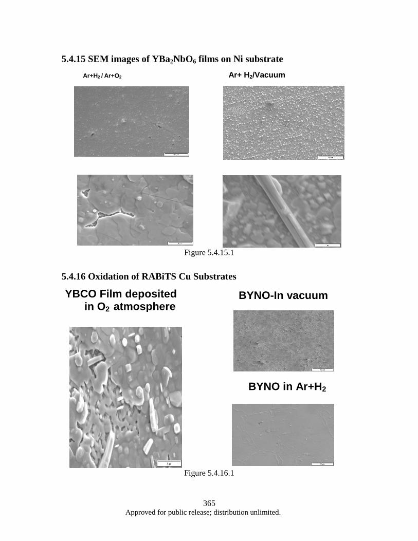
5.4.15 SEM images of YBa2NbO6 films on Ni substrate
Figure 5.4.15.1
5.4.16 Oxidation of RABiTS Cu Substrates
Figure 5.4.16.1
YBCO Film deposited in O2 atmosphere
BYNO-In vacuum
BYNO in Ar+H2
Ar+ H2/Vacuum Ar+H2 / Ar+O2

366 Approved for public release; distribution unlimited.
Possible solutions
1. IBAD process for oxide buffers on Metal Substrates
2. Deposit oxidation resistant metals using sputtering or ion beam sputtering
methods in order to stop RABiTS substrate to get oxidized.
3. Possible metals: Pt, Ag, Au, Ru, Rh, Ir, Pd etc.
5.4.17 IBAD system for coated conductor applications
Figure 5.4.17.1
• ~900 liter UHV Chamber
• 4-Axis All Metal Sealed Scanner (X, Y, Y, Z)
• 20 cm RF Ion Source ( NORDIKO)
– Hollow Cathode Neutralizers
• 3 cm Kaufman Ion Source ( COMMON WEALTH)
• 2 Off-Axis Residual Gas Analyzers
• Substrate heater ~ 1000 oC
• 1x1 sq foot uniformity with double side reel to reel coating
Figure 5.4.17.2

367 Approved for public release; distribution unlimited.
5.4.18 Schematic of the Experiment
Figure 5.4.18.1
NEUTRALIZERS (2)
TUNER
20cm RF ION SOURCE
SAMPLE MOUNT
SCANNER
Ar
CH4/H2/Ar/O
2
Single Beam Mode
Ar/O
2
3cm ION SOURCE SPUTTER
TARGET
Dual Beam Mode

368 Approved for public release; distribution unlimited.
5.4.19 Substrate Holder
Figure 5.4.19.1

369 Approved for public release; distribution unlimited.
5.4.20 YSZ Film on Si (6” dia) Substrate
Figure 5.4.20.1
5.4.21 Ru film on Si substrate
Figure 5.4.21.1

370 Approved for public release; distribution unlimited.
5.4.22 Mg Film using ISD
Figure 5.4.22.1
5.4.23 Ru Film on Cu substrate
Figure 5.4.23.1
5.4.24 Work Progress on Cera-flex substrates
• Cera Flex is a flexible YSZ tape with different Yittria concentrations
• When Yittria is 3% then it is more flexible like metal
• As obtained Ceraflex samples are 10-50 nm rough.
• We are trying to polish them using different techniques to achieve 2 nm
roughness to deposit IBAD YSZ and subsequent YBCO film
• WHY CERA FLEX? Our objective is to minimize AC Losses. If the substrate is
a non-metal it is an interesting situation for lot of applications.
0
1500
3000
4500
6000
7500
9000
35 40 45 50 55 60 65 70
2 Theta (o)
Inte
nsit
y (
arb
.un
its)
100
Cu
30nm film shows (100) orientation on
poly copper
Mg on Si(100) Mg on Cu substrate

371 Approved for public release; distribution unlimited.
5.5 COATED CONDUCTORS ON FLEXIBLE SUBSTRATES
References: N/A
Srinivas Sathiraju,
Air Force Research Laboratory, Wright- Patterson Air Force Base, OH
Presented at CEC-ICMC 2005
5.5.1 Our Team
• GEORGE - Flexible Ceraflex Substrates
• WILLIAM C LANTER- IBAD
• PANI – Cu substrate
• SCOTT APT & ANDY- FIB, Cross sectional studies
• TIM HAUGAN - In filed measurements
• PAUL N BARNES – Program Manager
5.5.2 ACKNOLEDGEMENTS
• Laraba Kendig – For XRD help
• Iman Maartense - AC susceptability measurements
• Angela Campbell for AFM measurements
• Irene, John Murphy and Lyle Brunke
• AFOSR, PR, AFRL and NRC for the research support
5.5.3 Out Line of Talk
• Objectives
• Experimental
• Our efforts on Cera-Flex substrates (IBAD- PLD)
• Our efforts on Texturing of metals on polished metal substrates Using IBAD
• Our efforts on Texturing of metals (Rh) on RABITs Ni or Cu based substrates
• Status on YBCO film deposition
• Conclusions

372 Approved for public release; distribution unlimited.
5.5.4 What is the Present Status
Figure 5.5.4.1
5.5.5 Objective of our Work
• Ceraflex work is mainly focused on minimizing Eddy Current losses in base
substrate
• Metallic buffer path for thermally and electrically stable conductor
What is the need ??
• Engineering applications Je Total thickness including the substrate and buffer
layers is considered.
• At present stabilizing layer thickness is 75 microns.
• If we use Cu substrate or Cu-Fe bi-axially oriented substrate or stainless steel with
a conducting path may eliminate the need for the stabilization layers
Figure 5.5.5.1
5.5.6 Why Copper Substrate???
• Low ferromagnetic losses in ac applications
• High thermal and electrical conductivity (useful for thermal stabilization) and
Motor industry is comfortable in using Copper based technology
Copper Stabilizer
Buffer Layers
HTS Layer
Biaxially Textured Metal Substrate or Polished metal
substrate
Silver Protective Layer

373 Approved for public release; distribution unlimited.
• Lower cost (5-6 times less than Ni alloys)
• Compatible to IBAD or RABITS methods
5.5.7 IBAD SYSTEM FOR CERAFLEX
Figure 5.5.7.1
5.5.8 Schematic of the Experiment
Figure 5.5.8.1
5.5.9 IBAD SYSTEM DETAILS
• ~900 liter UHV Chamber
• 4-Axis All Metal Sealed Scanner (X, Y, Y, Z)
• 20 cm RF Ion Source (NORDIKO)
– Hollow Cathode Neutralizers
• 3 cm Kaufman Ion Source (COMMON WEALTH)
• 2 Off-Axis Residual Gas Analyzers
• Substrate heater ~ 1000 oC
• 1x1 sq foot uniformity with double side reel to reel coating
NEUTRALIZERS (2)
TUNER
20cm RF
ION SOURCE
SAMPLE MOUNT
SCANNER
Ar
CH4/H2/Ar/O
2
Single Beam Mode

374 Approved for public release; distribution unlimited.
5.5.10 Substrate Holder (stationary substrates)
Figure 5.5.10.1
5.5.11 Reel to reel
Figure 5.5.11.1
5.5.12 Double side coating
Figure 5.5.12.1
5.5.13 Work Progress on Cera-flex substrates
• Cera Flex is a flexible YSZ tape with different Yittria concentrations
• When Yittria is 3% then it is more flexible like metal

375 Approved for public release; distribution unlimited.
• WHY CERA FLEX?? : Our objective is to minimize eddy current Losses. Also
for high sensitive SQUID
• As obtained Ceraflex samples are 50- 150 nm rough.
• We are trying to polish them using different techniques to achieve 2 nm
roughness to deposit IBAD YSZ and subsequent CeO2/ YBCO film
5.5.14 EFFORTS ON CERAFLEX
• We could achieve 10nm Ra with mechanical polishing
• YSZ films obtained till today are polycrystalline in nature
Figure 5.5.14.1
5.5.15 IBAD OF Mg Films
Figure 5.5.15.1 Figure 5.5.15.2
Figure 5.5.15.3
IBAD YSZ f ilm on Ceraf lex subst rat e
0
5000
10000
15000
20 25 30 35 40 45
2 Theta (o)
In
ten
sity (arb
.U
nits)
MG001
0
2000
4000
6000
8000
10000
12000
14000
16000
18000
20000
20 30 40 50 60
2 Theta (o)
Inte
ns
ity
(a
rb
.Un
its
)

376 Approved for public release; distribution unlimited.
5.5.16 Ru Film on Cu substrate • 300 nm film shows (100) orientation on polished copper
Figure 5.5.16.1 Figure 5.5.16.2
5.5.17 IBAD Ru Films on Cu substrate
No (100) growth
Figure 5.5.17.1
RU50113A
0
1000
2000
3000
4000
5000
6000
7000
8000
30 35 40 45 50 55 60
2 Theta (o)
Inte
ns
ity
(a
rb.U
nit
s)
0
1500
3000
4500
6000
7500
9000
35 40 45 50 55 60 65 70
2 Theta (o)
Inte
nsit
y (
arb
.un
its)
100 Cu

377 Approved for public release; distribution unlimited.
Growth in (100) direction
Figure 5.5.17.2
5.5.18 Pulsed Laser Deposition Parameters
Deposition Conditions Rh Films
Deposition pressure 10-5 Torr
Deposition Temperature RT -850 oC
Pulsed Laser Energy 2-3 J/cm2
Repetition Rate 10 Hz
Thickness 200 – 2000nm
Substrates STO,Cu-Fe, Ni-W, Cu
Figure 5.5.18.1
RU5012A
0
500
1000
1500
2000
2500
3000
3500
4000
4500
5000
25 30 35 40 45 50
2 Theta (o)
Inte
ns
ity
(a
rb.U
nit
s)

378 Approved for public release; distribution unlimited.
5.5.19 Rh films on Bi-axially textured Ni-W alloy deposited at RT
Figure 5.5.19.1
5.5.20 Rh films deposited at 700 C
FWHM ~ 6°
Figure 5.5.20.1 Figure 5.5.20.2
200 Ni-W
0
3000
6000
9000
12000
40 45 50
2 Theta (o)
Inten
sit
y (
arb
.Un
its)
0
1500
3000
4500
6000
35 40 45 50 55 60 65 70 75
2 Theta Intensity
Inte
nsit
y (
arb
.un
its
)(111)
(200)
Ni-W

379 Approved for public release; distribution unlimited.
5.5.21 FIB X-section of Rh/Ni-W
Rh Films were deposited at 785 °C
Figure 5.5.21.1 Figure 5.5.21.2
Efforts on YBCO growth
First YBCO film on 08/03
Ni-w/Rh/YBCO Ni-W/Rh/5%Ag doped YBCO
Figure 5.5.22.1 Figure 5.5.22.2
What next??? • Further improving the properties YBCO films
• Biaxially textured Cu or Ni-alloy/Rh/m-ABO3/Y123 (RABITS process)
• Polished Cu/ IBAD TiN/ IBAD Rh/ SrRuO3/ Y123
• Polished Cu/IBAD Rh/ conducting ABO3 /Y123
Summary • Ceraflex substrates are attractive for certain applications but average surface
roughness has to be improved in order to prove the concept.
• Metal buffers with another conducting oxide layer work is in progress
• Preliminary results are promising
-1
-0.8
-0.6
-0.4
-0.2
0
0 10 20 30 40 50TEMPERATURE (K)
'
0.025 Oe
0.1 Oe
0.25 Oe
0.5 Oe
1.0 Oe
1.5 Oe
2.2 Oe
SS162B
-1
-0.9
-0.8
-0.7
-0.6
-0.5
-0.4
-0.3
-0.2
-0.1
0
70 75 80 85
TEMPERATURE (K)
X' 0.025 Oe
0.1 Oe
0.25 Oe
0.5 Oe
1.0 Oe
1.5 Oe
2.2 Oe

380 Approved for public release; distribution unlimited.
Appendix
A.1 References
1. T. Haugan, P.N. Barnes, R. Wheeler, F. Meisenkothen, M. Sumption, Addition of
nanoparticles dispersion to enhance flux pinning of YBa2Cu3O7-x films, Nature
430, pp. 867 (2004).
2. T.J. Haugan,, P.N. Barnes, I. Maartense, E.J. Lee, M. Sumption, and C.B. Cobb,
Island growth of Y2BaCuO5 nanoparticles in (211~1.5nm/123~10nm)xN composite
multilayer structures to enhance flux pinning of YBa2Cu3O7-d films, J. Mater. Res.
18, 2618-2623 (2003).
3. T.A. Campbell, T.J. Haugan, P.N. Barnes, I. Maartense, J. Murphy, L. Brunke,
J.M. Evans, J. Kell, N. Yust, S. Sathiraju, Flux Pinning Effects of Y2O3 in YBCO
Thin Films as Nanoparticulate Multilayered Dispersions, J. Mater. Res.,
accepted.
4. T. Haugan, P. Barnes, I. Maartense, L. Brunke, and J. Murphy, Effect of O2
Partial Pressure on YBa2Cu3O7-X Thin Film Growth by Pulsed Laser Deposition,
Physica C, 397, pp.47-57, (2003).
5. P. N. Barnes, P. T. Murray, T. Haugan, R. Rogow, G. P. Perram, In situ creation
of nanoparticles from YBCO by pulsed laser deposition, Physica C, 377, pp. 578,
(2002).
6. P. N. Barnes, T. J. Haugan, C. V. Varanasi, T. A. Campbell, Flux pinning
behavior of incomplete multilayered lattice structures in YBa2Cu3O7-d, Appl.
Phys. Lett., 85, pp. 4088 (2004).
7. J.Z. Wu, R.L.S. Emergo, J.Z. Wu, T. Haugan, T. A. Campbell, and P. Barnes,
Tuning porosity of YBa2Cu3O7-x vicinal films by insertion of Y2BaCu1O5
nanoparticles, Appl. Phys. Lett., accepted.
8. T.J. Haugan, P.N. Barnes, T.A. Campbell, A. Goyal, A. Gapud, L. Heatherly, and
S. Kang, Deposition of (Y2BaCuO5/YBa2Cu3O7-x)xN multilayer coated conductors
on Ni-based textured substrates, Physica C, 425, pp. 21 (2005).
9. T.J. Haugan, P.N. Barnes, T.A. Campbell, J.M. Evans, J.W. Kell, L.B.
Brunke, J.P. Murphy, J.C. Tolliver, C.V. Varanasi, I. Maartense, L. Civale, B.
Maiorov, W. Wong-Ng, L.P. Cook, Addition of Alternate Phase Nanoparticle
Dispersions to Enhance Flux Pinning of Y-Ba-Cu-O Thin Films, 15, pp. 3770
(2005).
10. P.N. Barnes, T.J. Haugan, M.D. Sumption, B.C. Harrison, Pinning Enhancement
of YBa2Cu3O7-d Thin Films with Y2BaCuO5 Nanoparticulates, IEEE Trans. on
Appl. Superconductivity, 15, pp. 3766 (2005).

381 Approved for public release; distribution unlimited.
11. S. Sathiraju, P. T. Murray, T. J. Haugan, R. M. Nekkanti, L. Brunke, I. Maartense,
A.L. Campbell, J. P. Murphy, J. C. Tolliver, and P. N. Barnes, Studies on
Nanoparticulate Inclusions in Y123 Thin Films, Ceramic Transactions, Vol. 149,
pp. 177, (2004).
12. T. Haugan, P. Barnes, R. Nekkanti, J.M. Evans, L. Brunke, I. Maartense, J.P.
Murphy, A. Goyal, A. Gapud, and L. Heatherly, Deposition of
(2111.0nm/12310nm)xN Multilayer Coated Conductors on Ni-based Substrates,
Functional Growth of Epitaxial Oxides, pp. 359, (2003).
13. P.N. Barnes, T.J. Haugan, M.D. Sumption, S. Sathiraju, J.M. Evans, and J.C.
Tolliver, YBa2Cu3O7-d Films with a Nanoparticulate Dispersion of Y2BaCuO5 for
Enhanced Flux Pinning, Trans. MRS-J, 29(4), pp. 1385, (2004).
14. T. Haugan, P. N. Barnes, J. M. Evans, J. C. Tolliver, L. Brunke, T. A. Campbell,
I. Maartense, W. Wong-Ng, L. P. Cook, M. Sumption, Flux pinning of
YBa2Cu3O7- by nanoparticle defect addition and RE substitution for Y and Ba, in
Extended Abstract: 2003 Japan-US Workshop on Superconductivity.
15. C. Varanasi, P.N. Barnes, J. Burke, J. Carpenter, T. J. Haugan, Controlled
Introduction of Flux Pinning Centers in YBa2Cu3O7-x Films During Pulsed
Laser Deposition, Appl. Phys. Lett., accepted.
16. C.V. Varanasi, J. C. Tolliver, T. J. Haugan, K. W. Schmaeman, S. Sathiraju, L.
B. Brunke, J. P. Murphy, I. Maartense, Jack Burke, Jason Carpenter, P. N. Barnes,
Nd doped YBa2Cu3O7-z Films Deposited by Pulsed Laser Deposition, IEEE Trans.
on Appl. Superconductivity, 15, pp. 3722 (2005).
17. S. Sathiraju, R. Wheeler, P. Barnes, T. Peterson, I. Maartense, A. Campbell, R.
Nekkanti, L. Brunke, N. Yust, K. Fields, T. Campbell, T. Haugan, J. Tolliver, S.
Velmulakonda, S. Mukhopadhyay, Q. Jia, P. Arendt, Phase Formation of
YBa2Cu3-xNbxOy Thin Films, Functional Growth of Epitaxial Oxides, pp. 367,
(2005).
18. J.W. Kell, T.J. Haugan, P.N. Barnes, M.F. Locke, and T.A. Campbell C.V.
Varanasi and L.B. Brunke, Processing and Characterization of
(Y1-xTbx)Ba2Cu3O7-z Superconducting Thin Films Prepared by Pulsed Laser
Deposition, Ceramic Transactions, 160, pp. 15 (2005).
19. W. Wong-Ng, L.P. Cook, J. Suh, R. Feenstra, T. Haugan, and P. Barnes, Phase
Equilibria of Ba-R-Cu-O for Coated-Conductor Applications (R=lanthanides
and Y), Physica C 408-410, pp. 20, (2004).
20. T. Haugan, J.C. Tolliver, J.M. Evans, J.W. Kell, Crystal Chemical Substitutions of
YBa2Cu3O7- to Enhance Flux Pinning, in "Studies of High Temperature

382 Approved for public release; distribution unlimited.
Superconductors", edited by A. Narlikar, Vol. 48, 49 (Nova Science Publishers,
Inc., New York NY, 2004).
21. T. J. Haugan, T.A. Campbell, I. Maartense, P. N. Barnes, Microstructural and
Superconducting Properties of (Y1-xEux)Ba2Cu3O7-x Thin Films: x = 0 to 1, J.
Mater. Res., draft.
22. T.J. Haugan, M.E. Fowler, J.C. Tolliver, P.N. Barnes, W. Wong-Ng, L.P. Cook,
Flux Pinning and Properties of Solid-Solution (Y,Nd)1+xBa2-xCu3O7-d
Superconductors, Ceramic Trans. 140, pp. 299 (2003).
23. T.J. Haugan, J.M. Evans, J.C. Tolliver, I. Maartense, P.N. Barnes, W. Wong-Ng,
L.P. Cook, R.D. Shull, Flux Pinning and Properties of Solid-Solution
(Y,Nd)1+xBa2-xCu3O7- Superconductors Processed in Air and Partial Oxygen
Atmospheres, in "Fabrication of High-Temperature Superconductors", Ceramic
Transactions, 149, pp.151-162 (2004).
24. J.W. Kell, T.J. Haugan, J.M. Evans, P.N. Barnes, C.V. Varanasi, L.B.
Brunke, J.P. Murphy, Tb and Ce Doped YBa2Cu3O7-x Films Processed by
Pulsed Laser Deposition, IEEE Trans. on Appl. Superconductivity, 15, 3726
(2005).
25. G.A. Levin, P.N. Barnes, Concept of Multiply Connected Superconducting Tapes,
IEEE Trans. on Appl. Superconductivity, 15, 2158 (2005).
26. G. A. Levin, P. N. Barnes, N. Amemiya, S. Kasai, K. Yoda, Z. Jiang, A.
Polyanskii, Magnetization Losses in Multiply Connected YBa2Cu3O7-d Coated
Conductors, J. Appl. Phys. accepted.
27. G.A. Levin, P.N. Barnes, N. Amemiya, S. Kasai, K. Yoda, and Z. Jiang,
Magnetization Losses in Multifilament Coated Superconductors, Appl. Phys.
Lett., 86, pp. 72509, (2005).
28. N. Amemiya, S. Kasai, K. Yoda, Z. Jiang, G.A. Levin, P.N. Barnes, and C.E.
Oberly, AC loss reduction of YBCO coated conductors by multifilamentary
structure, Supercond. Sci. Technol., 17, pp. 1464 (2004).
29. Wang L. B. ; Selby P. ; Khanal C. ; Levin G. ; Haugan T. J. ; Barnes P. N. ; Kwon
C., The Distribution of Transport Current in YBCO Coated Conductor With
Zipper Striations, IEEE Trans. on Appl. Superconductivity, 15, pp. 2950 (2005).
30. Majoros M. ; Glowacki B. A. ; Campbell A. M. ; Levin G. A. ; Barnes P. N. ;
Polak M., AC Losses in Striated YBCO Coated Conductors, IEEE Trans. on Appl.
Superconductivity, 15, pp. 2819 (2005).

383 Approved for public release; distribution unlimited.
31. N. Amemiya, K. Yoda, S. Kasai, Zhenan Jiang, G.A.Levin, P.N. Barnes, and C.E.
Oberly, AC Loss Characteristics of Multifilamentary YBCO Coated Conductors,
IEEE Trans. on Appl. Superconductivity, 15, pp.1637 (2005).
32. M. Majoros, B. A. Glowacki, A. M. Campbell, G. A. Levin, P. N. Barnes,
Transport AC losses in striated YBCO coated conductors, Proceedings of the
European Conference of Applied Superconductivity, submitted.
33. C. V. Varanasi, N. Yust, P. N. Barnes, Biaxially Textured Copper-Iron Alloy
Substrates used in YBCO Coated Conductors, J. Mater. Res., submitted.
34. P. N. Barnes, S. M. Mukhopadhyay, S. Krishnaswami, T.J. Haugan, J.C. Tolliver,
and I. Maartense, Correlation between the XPS peak shapes of YBa2Cu3O7-x and
film quality, IEEE Trans. on Appl. Superconductivity, 13, pp. 3643, (2003).
35. C.V. Varanasi, G. Landis, P.N. Barnes, J. Burke, N. Yust, T. Haugan, Ni-20%Cr
Coatings on Biaxially Textured Copper and Copper-Iron Alloy Substrates for
YBa2Cu3O7-x Coated Conductor Applications, Ceramic Transactions, submitted.
36. S. Sathiraju, P.N. Barnes Q.X. Jia, and P.N. Arendt, Growth of YBa2Cu3O7-x films
on Ba2YNbO6 dielectric buffer layer on a biaxially oriented MgO template for
coated conductor applications, Supercond. Sci. Technol., submitted.
37. S. Sathiraju, P. N. Barnes, C. V. Varanasi, R. Wheeler, Studies on YBa2NbO6
buffer layers, Ceramic Transactions, 15, pp. 3009 (2005).
38. S. Sathiraju, N.A. Yust, R.N. Nekkanti, I. Martense, A.L. Campbell, T.L.
Peterson, T.J. Haugan, J.C. Tolliver, and P.N. Barnes, Growth Optimization of
YBa2NbO6 Buffer Layers, Mat. Res. Soc. Symp. Proc., EXS-3, pp. EE8.7.1-3
(2004).
39. S. Sathiraju, R.A. Wheeler, P.N. Barnes, Pulsed Laser deposited YBa2Cu2NbOy
thin films on SrTiO3 Substrate, Mat. Res. Soc. Symp. Proc., submitted.