Studies of Transmission and Reflection for an Anisotropic ... evan.pdf · Studies of Transmission...
18
Studies of Transmission and Reflection for an Anisotropic Thin Film System College of William & Mary Physics Department Senior Research Evan Crisman Adviser: Irina Novikova Abstract: Vanadium Dioxide thin films have long been a subject of study because of Vanadium Dioxide’s unique properties. Vanadium Dioxide, when heated, exhibits a sharp change in conductivity; changing from an insulating medium to a conducting one. This has led to its use in a number of industries, especially in the engineering fields. A number of different types of measurements have been made to characterize this unusual change in electrical properties, including stress & strain and electrical measurements 2 , as well as optical measurements. To help better understand the metal-insulator transition we have been making optical measurements with both continuous-wave and pulsed lasers of Vanadium Dioxide thin films grown on various substrates, including quartz, sapphire, and rutile 1 . Through my measurements, we found a continuous optical and electrical anisotropy for Vanadium Dioxide thin films grown on rutile (TiO2).
Transcript of Studies of Transmission and Reflection for an Anisotropic ... evan.pdf · Studies of Transmission...

Studies of Transmission and Reflection for an Anisotropic Thin Film System College of William & Mary Physics Department Senior Research
Evan Crisman Adviser: Irina Novikova
Abstract:
Vanadium Dioxide thin films have long been a subject of study because of Vanadium
Dioxide’s unique properties. Vanadium Dioxide, when heated, exhibits a sharp change in
conductivity; changing from an insulating medium to a conducting one. This has led to its use
in a number of industries, especially in the engineering fields. A number of different types of
measurements have been made to characterize this unusual change in electrical properties,
including stress & strain and electrical measurements2, as well as optical measurements. To help
better understand the metal-insulator transition we have been making optical measurements
with both continuous-wave and pulsed lasers of Vanadium Dioxide thin films grown on
various substrates, including quartz, sapphire, and rutile1. Through my measurements, we
found a continuous optical and electrical anisotropy for Vanadium Dioxide thin films grown on
rutile (TiO2).

1
Introduction:
My work initially began by taking optical measurements of Vanadium Dioxide thin
films for various substrates using continuous-wave laser measurements. Kittiwatanakul et al.
had reported an electrical anisotropy for two orthogonal crystal orientations for single-crystal
VO2 grown on TiO2. Anisotropy is seen as a difference in properties for different directions,
such as crystal axis or the polarization of light, and is an unusual and interesting property. As
Vanadium Dioxides have been used in semiconductors and other electronics, anisotropy in
these structures has potential for future engineering uses. Because optical computing is a
growing field, potential uses for thin films with optical anisotropy also exist. Thus a structure
which exhibits the metal-insulator transition of Vanadium Dioxide and also interesting optical
properties could be extremely useful.
Another driving force for optical measurements is to develop a better understanding of
the metal-insulator transition. The metal-insulator transition is extremely fast, and so it has been
historically difficult to view the change as it occurs at the molecular level. Because of this, our
optical measurements have been divided into two types. The first, for which I was largely
responsible, were continuous-wave measurements. These are able to detect the slower optical
effects of the transition as it occurs, namely changes in reflection and transmission. We observed
a high reflection for the insulating stage, followed by a sharp drop-off as the thin film system
was heated and passed into the metal stage. As the sample cools and reverts back to the
insulator stage the reflection of the sample increases. Because of this, we are able to use
reflection measurements to characterize the metal-insulator transition of Vanadium Dioxide
thin films. These optical measurements also formed a baseline for the second types of
experiments, which were ultrafast pulsed laser measurements. These are able to detect fast
changes on the femtosecond scale which occur in the model. These results are addressed
elsewhere1, and are outside the scope of this paper. Our overall goal was to develop an
understanding of the optical properties of Vanadium Dioxide thin films through the metal-
insulator transition.
Experiment
(i) Optical Measurements
In order to take optical measurements through the metal-insulator transition, a
specialized apparatus was required which allowed us to heat and cool the sample through the
transition. This was accomplished by a Peltier cooler attached to a stand to which the sample
could be attached. Transmission and reflection measurements could then be obtained in the
standard way, by hitting the sample with a polarized beam and catching the reflected and
transmitted beams on a photodetector.

2
Figure 1: Optical Experimental Setup
For most substrates on which Vanadium Dioxide was grown, transmission and reflection can be
measured; however, our sample grown on rutile had an unpolished back which made
transmission measurements impossible. Optical measurements were taken through the metal-
insulator transition for each substrate for two orthogonal polarizations of the incoming beam.
Once the initial anisotropy was observed for Vanadium Dioxide on rutile, we also took
measurements at intermediate polarizations. A 780nm wavelength continuous-wave laser was
used for these measurements. For a comparison, we also took equivalent measurements for
Vanadium Dioxide grown on quartz, which is polycrystalline.
(ii) Electrical Measurements:
In order to make a comparison to the results of Kittiwatanakul et al1., we also needed to
take electrical measurements of the VO2 thin film on rutile. These measurements accomplished
three things. The first was to establish that our sample, which was an extended thin film
medium instead of a single crystal, still exhibited electrical anisotropy. The second was to
compare electrical anisotropy found in this extended medium to that found in the single crystal.
The third was to observe how electrical anisotropy changed between the two orthogonal
maxima. In order to do this, we used a four-point probe with a sample-holder modified so that
the angle of the sample could be changed and recorded. Resistivity measurements were taken at

3
Figure 2: Four-Point Probe; current is measured across two points and voltage is measured across the other
two, forming a simple circuit. Each contacts the surface of the thin film and the device uses Ohm’s law to
calculate sample resistance.
four different temperatures through the metal-insulator transition for a complete rotation of the
sample. Although the single-crystal measurements were made for conductivity, resistivity is
equivalent in determining changes in electrical properties.
Results:
(i) Optical Results
Figure 1: Hysteresis showing optical anisotropy for Vanadium Dioxide grown on Rutile

4
Figure 2: Hysteresis showing optical anisotropy for Vanadium Dioxide grown on Rutile (Normalized)
We observed an optical anisotropy for two orthogonal orientations of the sample for
Vanadium Dioxide grown on rutile. There is a marked difference between the non-normalized
reflection values we collected (Figure 1). In order to ensure that this difference was not simply
due to experimental error, we normalized the values (Figure 2) and found the anisotropy to still
be present, implying that the optical anisotropy is intrinsic to the film.
Figure 3: Continuous Anisotropy for Vanadium Dioxide Grown on Rutile
To expand upon our initial results, we also looked at differences in reflection with a change in
polarization angle over an entire circular rotation at room temperature. This showed that there
is a continuous change in reflection with change in polarization angle. There are no sharp
changes or irregularities which we could detect in the anisotropic properties of this thin film
system.

5
Figure 4: Hysteresis showing isotropy for Vanadium Dioxide grown on Quartz
For comparison, we found no anisotropy for Vanadium Dioxide thin films grown on Quartz
(Figure 4). This difference may be due to the difference in the substrate. Quartz by itself is
polycrystalline and so does not typically exhibit anisotropic behavior. Rutile, on the other hand,
is monocrystalline and does normally exhibit anisotropic behavior.
(ii) Electrical Results
Our resistivity measurements also showed a strong and continuous anisotropy through
the metal-insulator transition(Figures 5&6). These results are consistent with the results of
Kittiwatanakul et al.; however, our results show an approximately forty times reduction in
magnitude than that found for the single-crystal.
Figure 5: Electrical anisotropy through the metal-insulator transition for Vanadium Dioxide grown on Rutile
(linear scale)

6
Figure 6: Electrical anisotropy for Vanadium Dioxide grown on Rutile, two temperatures highlighted to
show the anisotropic behavior at each temperature
Modeling
Background
A major goal has been to develop a working computational model of thin-film
transmission and reflection for our Vanadium Dioxide systems. Fortunately, Yeh4 and Schubert3
have a well-developed general model for anisotropic thin-film systems based on Berreman’s
matrix formulation for thin film systems5. Matlab is uniquely to converting this mathematical
model to a computational one, and so our model has been developed in this system. Having a
working model for our measurements will allow us to better drive further experiments and get
a better understanding of the metal-insulator transition. While the existing models are suited for
one temperature, modifications had to be added in order to model transmission and reflection
coefficient change with temperature.
The model developed by the previously listed authors is very clever and takes
advantage of Maxwell’s equations and the boundary conditions between layers of the thin film
system. It is an extremely interesting and very cool application of linear algebra to a physical
system, and I highly recommend that the reader look into the cited papers; however, I will
briefly discuss the theory relevant to the computational model I have been developing.
The heart of the model is the general transfer matrix. What this essentially accomplishes
is the transfer and modification of the incoming electromagnetic wave using the boundary
conditions from the wave’s entry to its exit expressed as reflection, transmission, and entry
coefficients. In the general matrix form this is expressed as
(
) (
)(
)
Where A is the incoming field vector, B is the reflected wave vector, and C is the transmitted
field vector. A useful—and fairly accurate—way of envisioning this is as a simplified cartoon
instead of a matrix: the incident wave A comes in and hits the thin film system T. Part is
transmitted and comes out on the other side as C, another part is reflected back from T and so
stays on the same side as the incident wave.

7
The transfer matrix is the heart of the model; however, in our case we want to extract the
reflected and transmitted vectors so we can calculate the reflection and transmission
coefficients. Their components can be calculated from the matrix elements of T, as demonstrated
by Yeh4:
(
)
(
)
(
)
(
)
These can then be used to calculate the reflection coefficient ρ and transmission coefficient τ as
usual:
| |
| |
where ρ is the reflection coefficient and τ is the transmission coefficient.
While this approach is fairly straightforward on the surface, under the hood it gets much
more complicated. Schubert3 defines the transfer matrix as
∏
There are a few different approaches used to calculate these components depending on the
situation3,4,5; we selected the method devised by Schubert which was general enough for
anisotropic media and allowed us to use the inputs from our experimental data. In this case the
components are devised as follows:
(
)
(
√
√
)

8
where Φa is the incident angle of the incoming wave, na is the index of refraction of
where
(
)
where εmn are components of the dielectric tensor and is the x component of the
wave vector.
Upon seeing the multitude of matrices it should become apparent as to why we used
Matlab, a programming language designed to handle large matrix operations. Our Vanadium
Dioxide samples were composed of two layers: a substrate layer and the VO2 layer. Therefore
our general transfer matrix for our systems is given as
Results
Early results for the modeling are promising, and replicating our data for our examples
is largely limited by the availability of the proper material parameters. We first began with the
simplest model: modeling the transmission of light through a film of glass. This yielded the
expected results, with approximately 4% reflection and 96% transmission. Additionally, around
the Brewster angle we saw reflection drop off, also as we would expect. These results indicated
that our model was working as expected for simple systems, allowing us to delve into models of
interest, beginning with modeling our results for quartz.
There is a great deal of variation in the dielectric constant of Vanadium Dioxide with
temperature, which is further complicated by variation due to deposition technique, crystal
structure and so on. These have made measurements difficult7; however, Swan and De Smet
were able to use ellipsometry to find the refractive indices of a Vanadium Dioxide thin film at
room temperature and at 84 C, in other words, before and after the transition6. For room
temperature they found a refractive index of 2.82-0.317i and for 84 C they reported a refractive
index of 2.24-0.456i. We were therefore able to use these values to compare our model to the
experiment results we had before and after the transition.
We first looked at our simpler, isotropic quartz model. Using the standard value for the
refractive index of quartz of 1.5387, along with the Vanadium Dioxide layer thickness of 70nm
and quartz layer thickness of .5mm, we were able to calculate the reflection of our 780nm beam
for room temperature and high temperature. For these calculations we used an initial angle

9
value of 0 for simplicity. For room temperature RRT was calculated as 0.5752 and for high
temperature RHT was calculated to be .2035. This corresponds to a decrease in reflection from
the insulator to metal stage of 35.5%. In our experiment, from 29.05 C to 84.95 C we saw a 33.9%
decrease in reflection power, as shown in Figure 4. As the reflection and reflection power are
proportional, we can meaningfully compare the percent reduction in both. This comparison
shows that our model is accurately able to replicate our experimental results. The difference
between the two can likely be accounted for by the fact that our temperatures do not exactly
match up with those used to calculate refractive indices and changes in thin film thickness due
to changes in temperature.
For our Vanadium Dioxide grown on Rutile the procedure was slightly different.
Because the back of the sample was unpolished and opaque, we instead used a single-layer
model with the exit medium as rutile. From Palik, Ghosh, and Gorachand1’s Handbook of Optical
Constants of Solids, we obtained a refractive index of 2.484 for one polarization and 2.826 for the
other at room temperature and used the same parameters for Vanadium Dioxide. This gave a
reflection coefficient in one direction of .6646 and .7779 for the other. The second polarization
gives a reflection increase of 1.17 times over the first. From our experimental values we
measured reflection of 275 mW for our polarization and 111 mW for its orthogonal
polarization., which would give a 2.48 times increase. While we see anisotropy, it is not as great
as we might expect; however, there are a number of confounding variables here. For one, the
Handbook only offers values for the rutile index of refraction for certain wavelengths. While our
experiments used a wavelength of 780nm, the closest available index of refraction was for a
wavelength of 708.2nm. Additionally, these values were for a temperature of 25 C, whereas our
experimental measurements started at 29.05 C. Adjusting the wavelength and temperature can
cause fairly large perturbations the reflection and transmission coefficients with our model.
However, it is extremely unlikely that the large difference between the model and the
experimental results occurs simply because of these small sources of error. Instead, these results
indicate that the large anisotropy we observed for Vanadium Dioxide grown on rutile is not
simply due to the effect of the anisotropic substrate. This signifies that the optical parameters
for Vanadium Dioxide change when grown on rutile. As our current sample has an unpolished
back, and thus does not allow for transmission, we are currently unable to determine the values
of these altered optical parameters, however.
Overall these data indicate that our current assumptions do not give the full story
behind the optical anisotropy we find in Vanadium Dioxide thin films grown on rutile. While
our model works well for matching our isotropic results with the quartz substrate, it performs
less well for the anisotropic results on the rutile substrate, indicating that the anisotropy
observed for Vanadium Dioxide grown on rutile is not solely due to the effects of the substrate.
This suggests that there are significant differences in the parameters for the anisotropic thin film
system which bear further experimental investigation.

10
Conclusion:
We have found both electrical and optical anisotropies for Vanadium Dioxide thin films
grown on Titanium Dioxide (rutile) for an extended thin film system. The electrical results
match what has already been reported2, although the magnitude of the anisotropy is greatly
reduced from that found for the single crystal. Additionally, we showed that the change in
resistivity is continuous and periodic with changing orientation of the sample. We also found
an equivalent optical anisotropy for reflection intensity through the metal-insulator transition
with a dramatic difference in intensity for two orthogonal sample orientations. Changing the
polarization of the incoming beam gave a continuous and periodic change in optical properties,
similar to the electrical properties. We were able to successfully model changes in reflection for
Vanadium Dioxide grown on quartz using known parameters; however, attempts to model
Vanadium Dioxide grown on rutile were met with less success. These results indicate that the
anisotropy we observe in Vanadium Dioxide grown on rutile is not due to the effect of the rutile
substrate alone. Experimental constraints—namely that we are unable to measure transmission
from our Vanadium Dioxide on rutile sample—prevent us from measuring those parameters at
present. Hopefully future experiments with more suitable samples will allow us to extract the
optical parameters for Vanadium Dioxide grown on rutile and allow us to gain a better
understanding of the cause of this difference. Altogether Vanadium Dioxide grown on rutile
exhibits anisotropy in optical and electrical properties, which promise to have great potential in
both gaining a better understanding of the metal-insulator transition and as a material for use in
electronics applications.

11
Works Cited
1. Radue, Crisman, Wang, Kittiwatanakul, Lu, Wolf, Lukasew, Novikova “Substrate Effect on
Optical Properties of Insulator-Metal Transition in VO2 Thin Films” arXiv:1210.7746
2. Salinporn, Lu, Wolf. “Transport Anisotropy of Epitaxial VO2
Films near the Metal-Semiconductor Transition” Applied Physics Express , 091104
(20122)
3. Schubert. “Polarization-dependent Optical Parameters of Arbitrarily Anisotropic
Homogenous Layered Systems” Physical Review, Volume 53, Number 8. February 1996.
4. Pochi, Yeh. “Optics of Anisotropic Layered Media: A New 4 X 4 Matrix Algebra” Surface
Science 96 41-53. August 20, 1979.
5. Berreman, Dwight, “Optics in Stratified and Anisotropic Media: A 4 X 4 Matrix Formulation”
Journal of the Optical Society of America, Volume 62, Number 4, October 22, 1971.
6. Swann, De Smet “Ellipsometric Investigation of Vanadium Dioxide Films” Journal of Applied
Physics, 58, 1335 (1985).
7. Tobar, Ghosh, Gorachand. Handbook of Optical Constants of Solids. Academic Press, San Diego.
1998.

12
Appendix: Listings for Matlab Reflection and Transmission Model
Listing 1: RTCoefficientsIsotropicTransferMatrix.m
function [Tp] = RTCoefficientsIsotropicTransferMatrix(eps0,n,lambda,d,phi) % Evan Crisman 2012 % Creates the transfer matrix for a layer in an anisotropic thin film system. % eps0x,eps0y,eps0z are the x,y,z portions of the dielectric tensor. % lambda is the wavelength of the incoming wave % omega is the angular frequency of the incoming initial beam. % d is the thickness of the layer in meters. % n is the refractive index %% Creating the Dielectric Tensor: %(Assumes the orientation of the Cartesian Crystal Coordinate system is the % same as the laboratory system.) function DielectricTensor=DielectricTensorFn(eps0layer) DielectricTensor=zeros(3,3); DielectricTensor(1,1)=eps0layer; DielectricTensor(2,2)=eps0layer; DielectricTensor(3,3)=eps0layer; end
%% Creating the Delta Matrix kx=n*sin(phi); % The x component of the wave vector is necessary for the delta matrix. %Phi is the angle of the incoming beam from incident. %For incident light, phi is zero, and so kx=0 in this case. c=3e8; % Speed of light omega=2*pi*c/lambda; function DeltaMatrix=DeltaMatrixFn(DielectricTensor) DeltaMatrix=zeros(4,4); DeltaMatrix(1,1)=(-kx*DielectricTensor (3,1)./DielectricTensor(3,3)); DeltaMatrix(1,2)=(-kx*DielectricTensor (3,2)./DielectricTensor(3,3)); DeltaMatrix(1,4)=1-((kx^2)/DielectricTensor(3,3)); DeltaMatrix(2,3)=-1; DeltaMatrix(3,1)=DielectricTensor(2,3)*(DielectricTensor
(3,1)./DielectricTensor(3,3))-DielectricTensor(2,1); DeltaMatrix(3,2)=kx^2-
DielectricTensor(2,2)+(DielectricTensor(2,3)*(DielectricTensor
(3,2)./DielectricTensor(3,3))); DeltaMatrix(3,4)=kx*DielectricTensor (2,3)./DielectricTensor(3,3); DeltaMatrix(4,1)=DielectricTensor(1,1)-
(DielectricTensor(1,3)*DielectricTensor (3,1)./DielectricTensor(3,3)); DeltaMatrix(4,2)=DielectricTensor(1,2)-
(DielectricTensor(1,3)*DielectricTensor (3,2)./DielectricTensor(3,3)); DeltaMatrix(4,4)=-kx*DielectricTensor (1,3)./DielectricTensor(3,3); end %% Calculating the Transfer Matrix DielectricTensor=DielectricTensorFn(eps0);

13
DeltaMatrix=DeltaMatrixFn(DielectricTensor); Tp=expm(1i*(omega/c)*DeltaMatrix*d); end
Listing 2: RTCoefficientsAnisotropicTransferMatrix.m
function [Tp] =
RTCoefficientsAnisotropicTransferMatrix(eps0x,eps0y,eps0z,n,lambda,d,phi) % Evan Crisman 2012 % Creates the transfer matrix for a layer in an anisotropic thin film system. % eps0x,eps0y,eps0z are the x,y,z portions of the dielectric tensor. % lambda is the wavelength of the incoming wave % omega is the angular frequency of the incoming initial beam. % d is the thickness of the layer in meters. % n is the refractive index %% Creating the Dielectric Tensor: %(Assumes the orientation of the Cartesian Crystal Coordinate system is the % same as the laboratory system.) function
DielectricTensor=DielectricTensorFn(eps0xlayer,eps0ylayer,eps0zlayer) DielectricTensor=zeros(3,3); DielectricTensor(1,1)=eps0xlayer; DielectricTensor(2,2)=eps0ylayer; DielectricTensor(3,3)=eps0zlayer; end
%% Creating the Delta Matrix kx=n*sin(phi); % The x component of the wave vector is necessary for the delta matrix. %Phi is the angle of the incoming beam from incident. %For incident light, phi is zero, and so kx=0 in this case. c=3e8; % Speed of light omega=2*pi*c/lambda; function DeltaMatrix=DeltaMatrixFn(DielectricTensor) DeltaMatrix=zeros(4,4); DeltaMatrix(1,1)=(-kx*DielectricTensor (3,1)./DielectricTensor(3,3)); DeltaMatrix(1,2)=(-kx*DielectricTensor (3,2)./DielectricTensor(3,3)); DeltaMatrix(1,4)=1-((kx^2)/DielectricTensor(3,3)); DeltaMatrix(2,3)=-1; DeltaMatrix(3,1)=DielectricTensor(2,3)*(DielectricTensor
(3,1)./DielectricTensor(3,3))-DielectricTensor(2,1); DeltaMatrix(3,2)=kx^2-
DielectricTensor(2,2)+(DielectricTensor(2,3)*(DielectricTensor
(3,2)./DielectricTensor(3,3))); DeltaMatrix(3,4)=kx*DielectricTensor (2,3)./DielectricTensor(3,3); DeltaMatrix(4,1)=DielectricTensor(1,1)-
(DielectricTensor(1,3)*DielectricTensor (3,1)./DielectricTensor(3,3)); DeltaMatrix(4,2)=DielectricTensor(1,2)-
(DielectricTensor(1,3)*DielectricTensor (3,2)./DielectricTensor(3,3)); DeltaMatrix(4,4)=-kx*DielectricTensor (1,3)./DielectricTensor(3,3); end %% Calculating the Transfer Matrix DielectricTensor=DielectricTensorFn(eps0x,eps0y,eps0z); DeltaMatrix=DeltaMatrixFn(DielectricTensor); Tp=expm(1i*(omega/c)*DeltaMatrix*d);

14
end
Listing 3: RTCoefficientsTwoLayerIA.m
function [Rss,Rpp,Tss,Tpp] =
RTCoefficientsTwoLayerIA(eps0isotropic,eps0x,eps0y,eps0z,lambda,d1,d2,na,nf,p
hi) %IA stands for ISOTROPIC Layer followed by ANISOTROPIC Layer. %Calculates the transmission and reflection coefficients t and r for the s %and p polarizations. %eps0isotropic is the dielectric constant for the isotropic substrate %eps0x,eps0y,eps0z are the dielectric coefficients in each direction for %the anisotropic layer. %lambda is the wavelength of the incoming wave in meters %d is the thickness of the thin film layer. %rss is the s polarized reflection coefficient for an s-polarized incoming % wave. %rpp is the p polarized reflection coefficient for a p-polarized incoming % wave. %tss is the s polarized transmission coefficient for an s-polarized % incoming wave. %tpp is the p polarized transmission coefficient for a p-polarized incoming % wave. %n is the index of refraction of the first layer, and is the same at each %boundary. %na is the index of refraction of the entrance medium % nf is the index of refraction of the exit medium
%% Creation of the T Matrix % This matrix is used for calculating the Reflection and Transmission % coefficients. y=real(eps0isotropic); n=sqrt(y); % (i) Entry Matrix InvLa=RTCoefficientsIncidentIncidentMatrix(na); % (ii) Transfer Matrix(Layer 1) d1=-d1; TransferMatrix1=RTCoefficientsIsotropicTransferMatrix(eps0isotropic,n,lambda,
d1,phi); % (iii Transfer Matrix(Layer 2) d2=-d2; TransferMatrix2=RTCoefficientsAnisotropicTransferMatrix(eps0x,eps0y,eps0z,n,l
ambda,d2,phi); % (iii) Exit Matrix Lf=RTCoefficientsIncidentExitMatrix(na,nf); % (iv) General Transfer Matrix T T=InvLa*TransferMatrix1*TransferMatrix2*Lf;
%% Calculation of transmission and reflection coefficients rss=((T(2,1)*T(3,3))-(T(2,3)*T(3,1)))./((T(1,1)*T(3,3))-(T(1,3)*T(3,1))); rpp=((T(1,1)*T(4,3))-(T(4,1)*T(1,3)))./((T(1,1)*T(3,3))-(T(1,3)*T(3,1))); tss=(T(3,3))./((T(1,1)*T(3,3))-(T(1,3)*T(3,1))); tpp=(T(1,1))./((T(1,1)*T(3,3))-(T(1,3)*T(3,1))); Rss=Real(rss)^2;
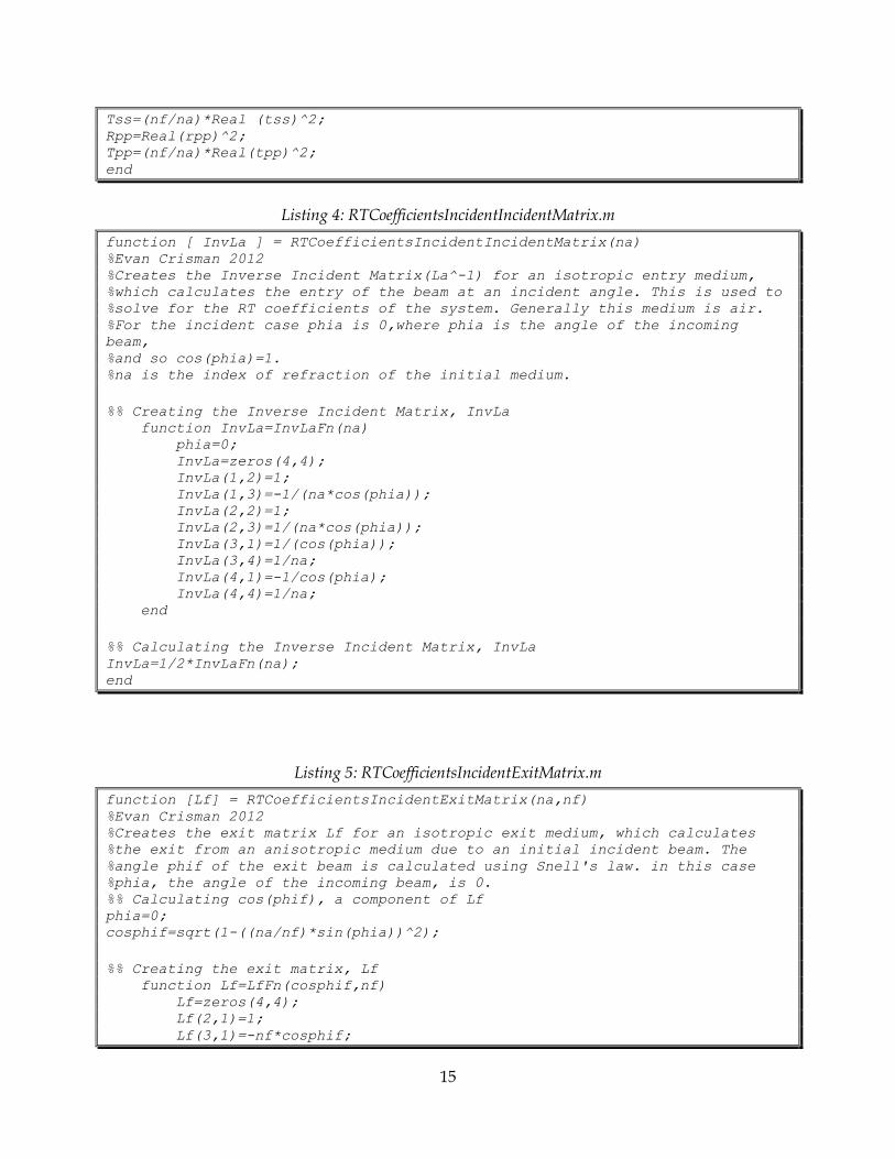
15
Tss=(nf/na)*Real (tss)^2; Rpp=Real(rpp)^2; Tpp=(nf/na)*Real(tpp)^2; end
Listing 4: RTCoefficientsIncidentIncidentMatrix.m
function [ InvLa ] = RTCoefficientsIncidentIncidentMatrix(na) %Evan Crisman 2012 %Creates the Inverse Incident Matrix(La^-1) for an isotropic entry medium, %which calculates the entry of the beam at an incident angle. This is used to %solve for the RT coefficients of the system. Generally this medium is air. %For the incident case phia is 0,where phia is the angle of the incoming
beam, %and so cos(phia)=1. %na is the index of refraction of the initial medium.
%% Creating the Inverse Incident Matrix, InvLa function InvLa=InvLaFn(na) phia=0; InvLa=zeros(4,4); InvLa(1,2)=1; InvLa(1,3)=-1/(na*cos(phia)); InvLa(2,2)=1; InvLa(2,3)=1/(na*cos(phia)); InvLa(3,1)=1/(cos(phia)); InvLa(3,4)=1/na; InvLa(4,1)=-1/cos(phia); InvLa(4,4)=1/na; end
%% Calculating the Inverse Incident Matrix, InvLa InvLa=1/2*InvLaFn(na); end
Listing 5: RTCoefficientsIncidentExitMatrix.m
function [Lf] = RTCoefficientsIncidentExitMatrix(na,nf) %Evan Crisman 2012 %Creates the exit matrix Lf for an isotropic exit medium, which calculates %the exit from an anisotropic medium due to an initial incident beam. The %angle phif of the exit beam is calculated using Snell's law. in this case %phia, the angle of the incoming beam, is 0. %% Calculating cos(phif), a component of Lf phia=0; cosphif=sqrt(1-((na/nf)*sin(phia))^2);
%% Creating the exit matrix, Lf function Lf=LfFn(cosphif,nf) Lf=zeros(4,4); Lf(2,1)=1; Lf(3,1)=-nf*cosphif;

16
Lf(1,3)=cosphif; Lf(4,3)=nf; end
%% Calculating the exit matrix, Lf Lf=LfFn(cosphif,nf); end
Listing 5: RTCoefficientsIncidentSingleLayer.m
function [Rss,Rpp,Tss,Tpp] =
RTCoefficientsIncidentSingleLayer(eps0x,eps0y,eps0z,lambda,d,na,nf) % Calculates the transmission and reflection coefficients t and r for the s % and p polarizations. %eps0x,eps0y,eps0z are the dielectric coefficients in each direction. %omega is the angular frequency of the incoming wave. %d is the thickness of the thin film layer. %rss is the s polarized reflection coefficient for an s-polarized incoming % wave. %rpp is the p polarized reflection coefficient for a p-polarized incoming % wave. %tss is the s polarized transmission coefficient for an s-polarized % incoming wave. %tpp is the p polarized transmission coefficient for a p-polarized incoming % wave. %na is the index of refraction of the entrance medium % nf is the index of refraction of the exit medium
%% Creation of the T Matrix % This matrix is used for calculating the Reflection and Transmission % coefficients.
% (i) Entry Matrix InvLa=RTCoefficientsIncidentIncidentMatrix(na); % (ii) Transfer Matrix(Layer) d=-d; TransferMatrix=RTCoefficientsIncidentTransferMatrix(eps0x,eps0y,eps0z,lambda,
d); % (iii) Exit Matrix Lf=RTCoefficientsIncidentExitMatrix(na,nf); % (iv) General Transfer Matrix T T=InvLa*TransferMatrix*Lf;
%% Calculation of transmission and reflection coefficients rss=((T(2,1)*T(3,3))-(T(2,3)*T(3,1)))./((T(1,1)*T(3,3))-(T(1,3)*T(3,1))); rpp=((T(1,1)*T(4,3))-(T(4,1)*T(1,3)))./((T(1,1)*T(3,3))-(T(1,3)*T(3,1))); tss=(T(3,3))./((T(1,1)*T(3,3))-(T(1,3)*T(3,1))); tpp=(T(1,1))./((T(1,1)*T(3,3))-(T(1,3)*T(3,1))); Rss=real(rss)^2; Tss=(nf/na)*real(tss)^2; Rpp=real(rpp)^2; Tpp=(nf/na)*real(tpp)^2; end
17
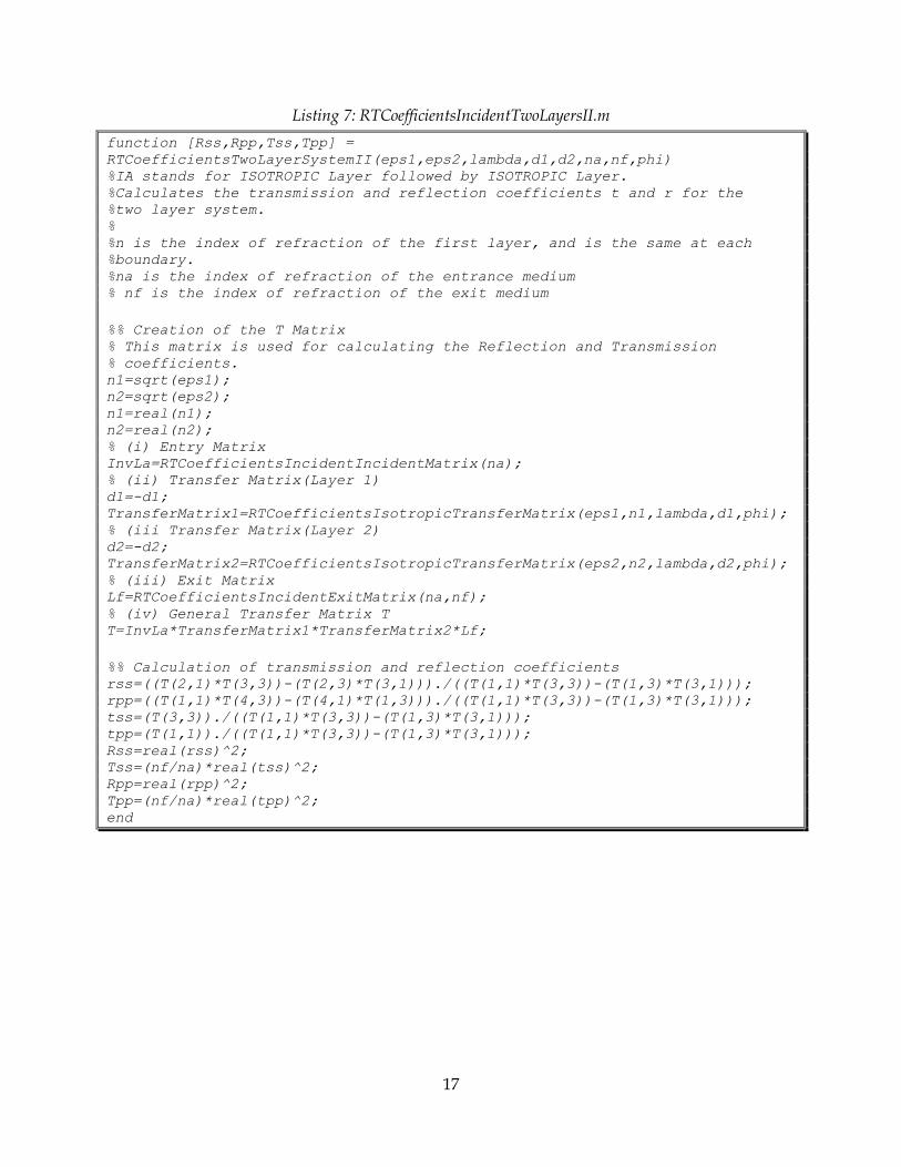
Listing 7: RTCoefficientsIncidentTwoLayersII.m
function [Rss,Rpp,Tss,Tpp] =
RTCoefficientsTwoLayerSystemII(eps1,eps2,lambda,d1,d2,na,nf,phi) %IA stands for ISOTROPIC Layer followed by ISOTROPIC Layer. %Calculates the transmission and reflection coefficients t and r for the %two layer system. % %n is the index of refraction of the first layer, and is the same at each %boundary. %na is the index of refraction of the entrance medium % nf is the index of refraction of the exit medium
%% Creation of the T Matrix % This matrix is used for calculating the Reflection and Transmission % coefficients. n1=sqrt(eps1); n2=sqrt(eps2); n1=real(n1); n2=real(n2); % (i) Entry Matrix InvLa=RTCoefficientsIncidentIncidentMatrix(na); % (ii) Transfer Matrix(Layer 1) d1=-d1; TransferMatrix1=RTCoefficientsIsotropicTransferMatrix(eps1,n1,lambda,d1,phi); % (iii Transfer Matrix(Layer 2) d2=-d2; TransferMatrix2=RTCoefficientsIsotropicTransferMatrix(eps2,n2,lambda,d2,phi); % (iii) Exit Matrix Lf=RTCoefficientsIncidentExitMatrix(na,nf); % (iv) General Transfer Matrix T T=InvLa*TransferMatrix1*TransferMatrix2*Lf;
%% Calculation of transmission and reflection coefficients rss=((T(2,1)*T(3,3))-(T(2,3)*T(3,1)))./((T(1,1)*T(3,3))-(T(1,3)*T(3,1))); rpp=((T(1,1)*T(4,3))-(T(4,1)*T(1,3)))./((T(1,1)*T(3,3))-(T(1,3)*T(3,1))); tss=(T(3,3))./((T(1,1)*T(3,3))-(T(1,3)*T(3,1))); tpp=(T(1,1))./((T(1,1)*T(3,3))-(T(1,3)*T(3,1))); Rss=real(rss)^2; Tss=(nf/na)*real(tss)^2; Rpp=real(rpp)^2; Tpp=(nf/na)*real(tpp)^2; end