Structural and photo luminescent properties of uncapped nanocrystalline Cd1−xZnxS solid solutions
5
Structural and photo luminescent properties of uncapped nanocrystalline Cd 1x Zn x S solid solutions Sonia Arora, S. Sundar Manoharan * Materials’ Chemistry Laboratory, Department of Chemistry, Indian Institute of Technology Kanpur, Kanpur 208 016, India Received 17 September 2007; received in revised form 21 November 2007; accepted 21 February 2008 Available online 8 April 2008 Abstract Uncapped nanocrystalline Cd 1x Zn x S (0.0 6 x P 0.5) solid solution prepared by microwave assisted combustion route shows hexag- onal to cubic phase transformation for even low doping of zinc up to 5 at.% as evident from the X-ray diffraction patterns and the selected area electron diffraction patterns. The solid solutions show a considerable shift in the optical absorption edge from 2.43 eV (CdS) to 2.73 eV for the equi-atomic composition (Cd 0.5 Zn 0.5 S). The blue emission in CdS shows effect of quantum confinement. The photo luminescence spectra of Zn lean compositions (up to 5 at.%) show emergence of a peak at k 530 nm along with the blue emission features of CdS. However, solid solutions with higher zinc content (up to 50 at.%), show a systematic increase in the intensity of peak at 530 nm with a blue shift up to 30 at.% of zinc doping. Beyond 30%, a broad blue–green emission with full width at half max- ima of 100 nm for Cd 0.5 Zn 0.5 S is observed. Ó 2008 Elsevier B.V. All rights reserved. PACS: 78.55.C; 78.66.H Keywords: Phase transformation; Photo luminescence; Microwave synthesis; Quantum confinement 1. Introduction CdS and ZnS are well-known wide and direct band gap II–VI semiconductors with a band gap, E g of 2.42 (510 nm) and 3.68 eV (340 nm), respectively [1]. Quan- tization of band gap in CdS to achieve emission across the visible spectrum is well understood experimentally [2] and substantiated by theoretical studies [3]. Like wise, ZnS shows blue–green emission [4] arising from defect states. Since excitonic binding energy for bulk ZnS is 35 meV, which is comparable to thermal energy, bulk ZnS does not show the excitonic features at room temper- ature. However in nanocrystalline ZnS, the binding energy of the exciton is significantly increased due to quantum confinement therefore the excitonic transitions become apparent at room temperature [5]. In case of CdS, the band gap is studied to be tunable between 2.5 and 4.0 eV in nano-size regime [2]. ZnS and CdS form binary alloys [6,7] with relatively simple properties wherein band gap changes almost in proportion to the composition. For example, E g in Wurtzite Zn 1x Cd x S changes from 3.91 eV for ZnS to 2.58 eV in CdS. Emission spectra of cubic (Zn,Cd)S:Ag (0.005 wt%) is reported to cover the entire visible spectrum by varying the Zn 2+ /Cd 2+ ratio [6]. The ternary compounds of CdS and ZnS viz. Cd x Zn 1x S are investigated as promising materials for high-density optical recording and blue or UV laser diodes owing to the band gap tuning for CdS–ZnS solid solutions from green to UV light [8]. However, with different pre- parative routes, such alloys have shown either narrow or broad photo luminescent emission, for instance FWHM more than 80 nm due to high defect states [9] or FWHM 10–15 nm [10] can be tailored. In this report, we show the structural and optical properties of uncapped Cd 1x Zn x S 0925-3467/$ - see front matter Ó 2008 Elsevier B.V. All rights reserved. doi:10.1016/j.optmat.2008.02.011 * Corresponding author. Tel.: +91 512 2597425/6043; fax: +91 512 2597436/7425. E-mail address: [email protected] (S.S. Manoharan). www.elsevier.com/locate/optmat Available online at www.sciencedirect.com Optical Materials 31 (2008) 176–180
-
Upload
sonia-arora -
Category
Documents
-
view
212 -
download
0
Transcript of Structural and photo luminescent properties of uncapped nanocrystalline Cd1−xZnxS solid solutions
Available online at www.sciencedirect.com
www.elsevier.com/locate/optmat
Optical Materials 31 (2008) 176–180
Structural and photo luminescent properties ofuncapped nanocrystalline Cd1�xZnxS solid solutions
Sonia Arora, S. Sundar Manoharan *
Materials’ Chemistry Laboratory, Department of Chemistry, Indian Institute of Technology Kanpur, Kanpur 208 016, India
Received 17 September 2007; received in revised form 21 November 2007; accepted 21 February 2008Available online 8 April 2008
Abstract
Uncapped nanocrystalline Cd1�xZnxS (0.0 6 x P 0.5) solid solution prepared by microwave assisted combustion route shows hexag-onal to cubic phase transformation for even low doping of zinc up to 5 at.% as evident from the X-ray diffraction patterns and theselected area electron diffraction patterns. The solid solutions show a considerable shift in the optical absorption edge from �2.43 eV(CdS) to �2.73 eV for the equi-atomic composition (Cd0.5Zn0.5S). The blue emission in CdS shows effect of quantum confinement.The photo luminescence spectra of Zn lean compositions (up to 5 at.%) show emergence of a peak at k � 530 nm along with the blueemission features of CdS. However, solid solutions with higher zinc content (up to 50 at.%), show a systematic increase in the intensityof peak at 530 nm with a blue shift up to 30 at.% of zinc doping. Beyond 30%, a broad blue–green emission with full width at half max-ima of �100 nm for Cd0.5Zn0.5S is observed.� 2008 Elsevier B.V. All rights reserved.
PACS: 78.55.C; 78.66.H
Keywords: Phase transformation; Photo luminescence; Microwave synthesis; Quantum confinement
1. Introduction
CdS and ZnS are well-known wide and direct band gapII–VI semiconductors with a band gap, Eg of 2.42(�510 nm) and 3.68 eV (�340 nm), respectively [1]. Quan-tization of band gap in CdS to achieve emission acrossthe visible spectrum is well understood experimentally [2]and substantiated by theoretical studies [3]. Like wise,ZnS shows blue–green emission [4] arising from defectstates. Since excitonic binding energy for bulk ZnS is�35 meV, which is comparable to thermal energy, bulkZnS does not show the excitonic features at room temper-ature. However in nanocrystalline ZnS, the binding energyof the exciton is significantly increased due to quantumconfinement therefore the excitonic transitions become
0925-3467/$ - see front matter � 2008 Elsevier B.V. All rights reserved.
doi:10.1016/j.optmat.2008.02.011
* Corresponding author. Tel.: +91 512 2597425/6043; fax: +91 5122597436/7425.
E-mail address: [email protected] (S.S. Manoharan).
apparent at room temperature [5]. In case of CdS, the bandgap is studied to be tunable between 2.5 and 4.0 eV innano-size regime [2]. ZnS and CdS form binary alloys[6,7] with relatively simple properties wherein band gapchanges almost in proportion to the composition. Forexample, Eg in Wurtzite Zn1�xCdxS changes from3.91 eV for ZnS to 2.58 eV in CdS. Emission spectra ofcubic (Zn,Cd)S:Ag (0.005 wt%) is reported to cover theentire visible spectrum by varying the Zn2+/Cd2+ ratio[6]. The ternary compounds of CdS and ZnS viz.CdxZn1�xS are investigated as promising materials forhigh-density optical recording and blue or UV laser diodesowing to the band gap tuning for CdS–ZnS solid solutionsfrom green to UV light [8]. However, with different pre-parative routes, such alloys have shown either narrow orbroad photo luminescent emission, for instance FWHMmore than �80 nm due to high defect states [9] or FWHM�10–15 nm [10] can be tailored. In this report, we show thestructural and optical properties of uncapped Cd1�xZnxS
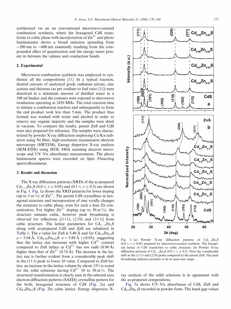
Fig. 1. (a) Powder X-ray diffraction patterns of Cd1�xZnxS(0.0 6 x P 0.05) prepared by microwave-assisted synthesis. The hexago-nal lattice of CdS transforms to cubic structure; (b) Powder X-raydiffraction patterns of Cd1�xZnxS (0.0 6 x P 0.5). Note the considerableshift in the (111) and (220) peaks compared to the parent ZnS. The peakbroadening indicates particles to be in nano-size range.
S. Arora, S.S. Manoharan / Optical Materials 31 (2008) 176–180 177
synthesized via an un conventional microwave-assistedcombustion synthesis, where the hexagonal CdS trans-forms to cubic phase with incorporation of Zn2+ and photoluminescence shows a broad emission spreading from�380 nm to �600 nm essentially resulting from the com-pounded effect of quantization and the energy states pres-ent in between the valence and conduction bands.
2. Experimental
Microwave combustion synthesis was employed to syn-thesize all the compositions [11]. In a typical reaction,desired amount of analytical grade cadmium nitrate, zincacetate and thiourea (as per oxidizer to fuel ratio [11]) weredissolved in a minimum amount of distilled water in a100 ml beaker and the contents were exposed to microwaveirradiation operating at 2450 MHz. The total reaction timeto initiate a combustion reaction and subsequently to formthe end product took less than 5 min. The product thusformed was washed with water and alcohol in order toremove any organic impurity and the samples were driedin vacuum. To compare the results, parent ZnS and CdSwere also prepared for reference. The samples were charac-terized by powder X-ray diffraction employing Cu Ka radi-ation using Ni filter, high-resolution transmission electronmicroscopy (HRTEM), Energy dispersive X-ray analysis(SEM-EDX) using JEOL 840A scanning electron micro-scope and UV–Vis absorbance measurements. The photoluminescent spectra were recorded on Spex Flourologspectroflourimeter.
3. Results and discussion
The X-ray diffraction patterns (XRD) of the as-preparedCd1�xZnxS (0.0 6 x 6 0.05) and (0.1 6 x 6 0.5) are shownin Fig. 1. Fig. 1a shows the XRD patterns for lower doping(up to 5 at.%) of Zn2+. The parent CdS crystallizes in hex-agonal structure and incorporation of zinc vividly changesthe structure to cubic phase, even for such a lean Zn con-centration. For higher Zn2+ doping (up to 50 at.%), thestructure remains cubic, however peak broadening isobserved for reflections [(1 11), (220) and (311)] fromcubic structure. The lattice parameters for Cd1�xZnxSalong with as-prepared CdS and ZnS are tabulated inTable 1. The a value for ZnS is 5.40 A and for Cd0.5Zn0.5Sa = 5.64 A, Cd0.95Zn0.05S a = 5.89 A (±0.03); suggestingthat the lattice size increases with higher Cd2+ contentcompared to ZnS lattice as Cd2+ has ion radii (0.90 A)higher than that of Zn2+ (0.74 A). The increase in the lat-tice size is further evident from a considerable peak shiftin the (111) peak to lower 2h value. Compared to ZnS lat-tice, an increase in the lattice volume by about 15% is notedfor the solid solutions having Cd2+ 10 to 50 at.%. Thestructural transformation is clearly seen in the selected areaelectron diffraction patterns (SAED); crystalline pattern forthe both; hexagonal structure of CdS (Fig. 2a) andCd0.5Zn0.5S (Fig. 2b) cubic lattice. Energy dispersive X-
ray analysis of the solid solutions is in agreement withthe as-prepared compositions.
Fig. 3a shows UV–Vis absorbance of CdS, ZnS andCd0.5Zn0.5S recorded in powder form. The band gap values
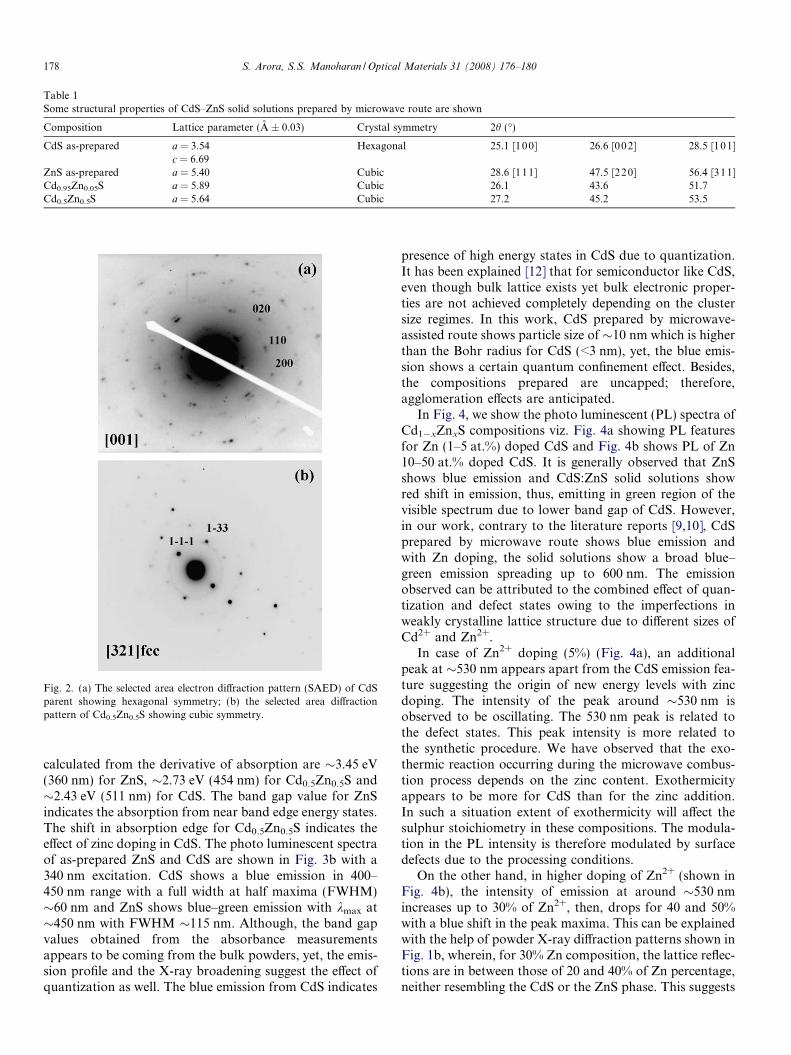
Table 1Some structural properties of CdS–ZnS solid solutions prepared by microwave route are shown
Composition Lattice parameter (A ± 0.03) Crystal symmetry 2h (�)
CdS as-prepared a = 3.54 Hexagonal 25.1 [100] 26.6 [002] 28.5 [101]c = 6.69
ZnS as-prepared a = 5.40 Cubic 28.6 [111] 47.5 [220] 56.4 [311]Cd0.95Zn0.05S a = 5.89 Cubic 26.1 43.6 51.7Cd0.5Zn0.5S a = 5.64 Cubic 27.2 45.2 53.5
Fig. 2. (a) The selected area electron diffraction pattern (SAED) of CdSparent showing hexagonal symmetry; (b) the selected area diffractionpattern of Cd0.5Zn0.5S showing cubic symmetry.
178 S. Arora, S.S. Manoharan / Optical Materials 31 (2008) 176–180
calculated from the derivative of absorption are �3.45 eV(360 nm) for ZnS, �2.73 eV (454 nm) for Cd0.5Zn0.5S and�2.43 eV (511 nm) for CdS. The band gap value for ZnSindicates the absorption from near band edge energy states.The shift in absorption edge for Cd0.5Zn0.5S indicates theeffect of zinc doping in CdS. The photo luminescent spectraof as-prepared ZnS and CdS are shown in Fig. 3b with a340 nm excitation. CdS shows a blue emission in 400–450 nm range with a full width at half maxima (FWHM)�60 nm and ZnS shows blue–green emission with kmax at�450 nm with FWHM �115 nm. Although, the band gapvalues obtained from the absorbance measurementsappears to be coming from the bulk powders, yet, the emis-sion profile and the X-ray broadening suggest the effect ofquantization as well. The blue emission from CdS indicates
presence of high energy states in CdS due to quantization.It has been explained [12] that for semiconductor like CdS,even though bulk lattice exists yet bulk electronic proper-ties are not achieved completely depending on the clustersize regimes. In this work, CdS prepared by microwave-assisted route shows particle size of �10 nm which is higherthan the Bohr radius for CdS (<3 nm), yet, the blue emis-sion shows a certain quantum confinement effect. Besides,the compositions prepared are uncapped; therefore,agglomeration effects are anticipated.
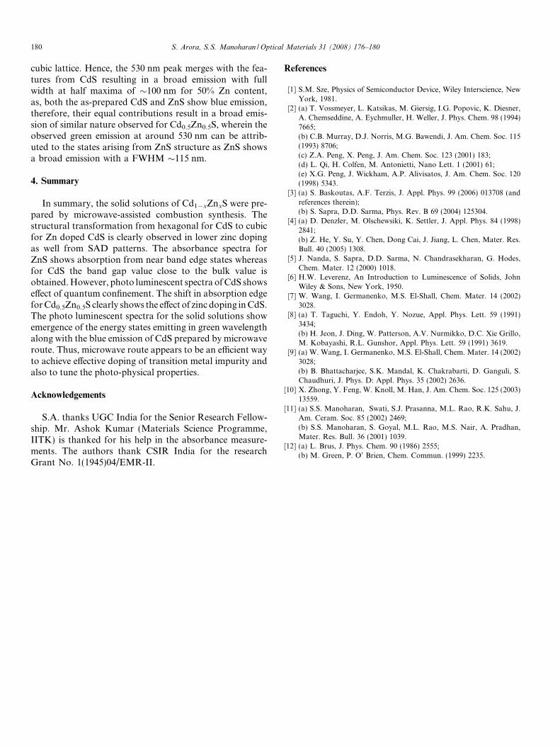
In Fig. 4, we show the photo luminescent (PL) spectra ofCd1�xZnxS compositions viz. Fig. 4a showing PL featuresfor Zn (1–5 at.%) doped CdS and Fig. 4b shows PL of Zn10–50 at.% doped CdS. It is generally observed that ZnSshows blue emission and CdS:ZnS solid solutions showred shift in emission, thus, emitting in green region of thevisible spectrum due to lower band gap of CdS. However,in our work, contrary to the literature reports [9,10], CdSprepared by microwave route shows blue emission andwith Zn doping, the solid solutions show a broad blue–green emission spreading up to 600 nm. The emissionobserved can be attributed to the combined effect of quan-tization and defect states owing to the imperfections inweakly crystalline lattice structure due to different sizes ofCd2+ and Zn2+.
In case of Zn2+ doping (5%) (Fig. 4a), an additionalpeak at �530 nm appears apart from the CdS emission fea-ture suggesting the origin of new energy levels with zincdoping. The intensity of the peak around �530 nm isobserved to be oscillating. The 530 nm peak is related tothe defect states. This peak intensity is more related tothe synthetic procedure. We have observed that the exo-thermic reaction occurring during the microwave combus-tion process depends on the zinc content. Exothermicityappears to be more for CdS than for the zinc addition.In such a situation extent of exothermicity will affect thesulphur stoichiometry in these compositions. The modula-tion in the PL intensity is therefore modulated by surfacedefects due to the processing conditions.
On the other hand, in higher doping of Zn2+ (shown inFig. 4b), the intensity of emission at around �530 nmincreases up to 30% of Zn2+, then, drops for 40 and 50%with a blue shift in the peak maxima. This can be explainedwith the help of powder X-ray diffraction patterns shown inFig. 1b, wherein, for 30% Zn composition, the lattice reflec-tions are in between those of 20 and 40% of Zn percentage,neither resembling the CdS or the ZnS phase. This suggests
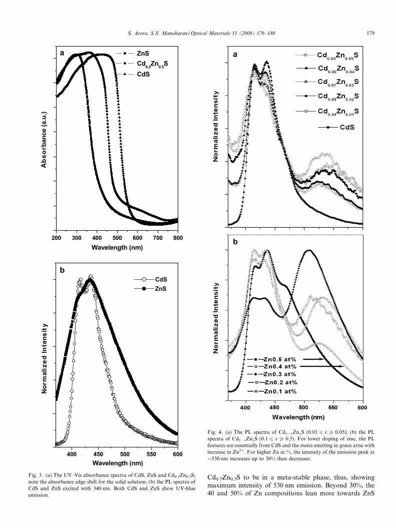
Fig. 3. (a) The UV–Vis absorbance spectra of CdS, ZnS and Cd0.5Zn0.5S;note the absorbance edge shift for the solid solution, (b) the PL spectra ofCdS and ZnS excited with 340 nm. Both CdS and ZnS show UV-blueemission.
Fig. 4. (a) The PL spectra of Cd1�xZnxS (0.01 6 x P 0.05); (b) the PLspectra of Cd1�xZnxS (0.1 6 x P 0.5). For lower doping of zinc, the PLfeatures are essentially from CdS and the states emitting in green arise withincrease in Zn2+. For higher Zn at.%, the intensity of the emission peak at�530 nm increases up to 30% then decreases.
S. Arora, S.S. Manoharan / Optical Materials 31 (2008) 176–180 179
Cd0.7Zn0.3S to be in a meta-stable phase, thus, showingmaximum intensity of 530 nm emission. Beyond 30%, the40 and 50% of Zn compositions lean more towards ZnS
180 S. Arora, S.S. Manoharan / Optical Materials 31 (2008) 176–180
cubic lattice. Hence, the 530 nm peak merges with the fea-tures from CdS resulting in a broad emission with fullwidth at half maxima of �100 nm for 50% Zn content,as, both the as-prepared CdS and ZnS show blue emission,therefore, their equal contributions result in a broad emis-sion of similar nature observed for Cd0.5Zn0.5S, wherein theobserved green emission at around 530 nm can be attrib-uted to the states arising from ZnS structure as ZnS showsa broad emission with a FWHM �115 nm.
4. Summary
In summary, the solid solutions of Cd1�xZnxS were pre-pared by microwave-assisted combustion synthesis. Thestructural transformation from hexagonal for CdS to cubicfor Zn doped CdS is clearly observed in lower zinc dopingas well from SAD patterns. The absorbance spectra forZnS shows absorption from near band edge states whereasfor CdS the band gap value close to the bulk value isobtained. However, photo luminescent spectra of CdS showseffect of quantum confinement. The shift in absorption edgefor Cd0.5Zn0.5S clearly shows the effect of zinc doping in CdS.The photo luminescent spectra for the solid solutions showemergence of the energy states emitting in green wavelengthalong with the blue emission of CdS prepared by microwaveroute. Thus, microwave route appears to be an efficient wayto achieve effective doping of transition metal impurity andalso to tune the photo-physical properties.
Acknowledgements
S.A. thanks UGC India for the Senior Research Fellow-ship. Mr. Ashok Kumar (Materials Science Programme,IITK) is thanked for his help in the absorbance measure-ments. The authors thank CSIR India for the researchGrant No. 1(1945)04/EMR-II.
References
[1] S.M. Sze, Physics of Semiconductor Device, Wiley Interscience, NewYork, 1981.
[2] (a) T. Vossmeyer, L. Katsikas, M. Giersig, I.G. Popovic, K. Diesner,A. Chemseddine, A. Eychmuller, H. Weller, J. Phys. Chem. 98 (1994)7665;(b) C.B. Murray, D.J. Norris, M.G. Bawendi, J. Am. Chem. Soc. 115(1993) 8706;(c) Z.A. Peng, X. Peng, J. Am. Chem. Soc. 123 (2001) 183;(d) L. Qi, H. Colfen, M. Antonietti, Nano Lett. 1 (2001) 61;(e) X.G. Peng, J. Wickham, A.P. Alivisatos, J. Am. Chem. Soc. 120(1998) 5343.
[3] (a) S. Baskoutas, A.F. Terzis, J. Appl. Phys. 99 (2006) 013708 (andreferences therein);(b) S. Sapra, D.D. Sarma, Phys. Rev. B 69 (2004) 125304.
[4] (a) D. Denzler, M. Olschewsiki, K. Settler, J. Appl. Phys. 84 (1998)2841;(b) Z. He, Y. Su, Y. Chen, Dong Cai, J. Jiang, L. Chen, Mater. Res.Bull. 40 (2005) 1308.
[5] J. Nanda, S. Sapra, D.D. Sarma, N. Chandrasekharan, G. Hodes,Chem. Mater. 12 (2000) 1018.
[6] H.W. Leverenz, An Introduction to Luminescence of Solids, JohnWiley & Sons, New York, 1950.
[7] W. Wang, I. Germanenko, M.S. El-Shall, Chem. Mater. 14 (2002)3028.
[8] (a) T. Taguchi, Y. Endoh, Y. Nozue, Appl. Phys. Lett. 59 (1991)3434;(b) H. Jeon, J. Ding, W. Patterson, A.V. Nurmikko, D.C. Xie Grillo,M. Kobayashi, R.L. Gunshor, Appl. Phys. Lett. 59 (1991) 3619.
[9] (a) W. Wang, I. Germanenko, M.S. El-Shall, Chem. Mater. 14 (2002)3028;(b) B. Bhattacharjee, S.K. Mandal, K. Chakrabarti, D. Ganguli, S.Chaudhuri, J. Phys. D: Appl. Phys. 35 (2002) 2636.
[10] X. Zhong, Y. Feng, W. Knoll, M. Han, J. Am. Chem. Soc. 125 (2003)13559.
[11] (a) S.S. Manoharan, Swati, S.J. Prasanna, M.L. Rao, R.K. Sahu, J.Am. Ceram. Soc. 85 (2002) 2469;(b) S.S. Manoharan, S. Goyal, M.L. Rao, M.S. Nair, A. Pradhan,Mater. Res. Bull. 36 (2001) 1039.
[12] (a) L. Brus, J. Phys. Chem. 90 (1986) 2555;(b) M. Green, P. O’ Brien, Chem. Commun. (1999) 2235.