Stoichiometric Boron-Based Nanostructures · 2018-09-25 · Stoichiometric Boron-Based...
24
2 Stoichiometric Boron-Based Nanostructures Limin Cao 1 , Xiangyi Zhang 1 , Wenkui Wang 1 and Min Feng 2 1 State Key Laboratory of Metastable Materials, Yanshan University 2 Department of Physics and Astronomy, University of Pittsburgh 1 China 2 USA 1. Introduction The elemental boron and boron-containing compounds hold a unique place in chemistry, physics, and materials science (Greenwood, 1973; Donohue, 1974; Matkovich, 1977; Emin, 1987; Albert & Hillebrecht, 2009). In general, they are composed of various multi-atom boron clusters, such as graphitic layer, octahedral B 6 and icosahedral B 12 , among which the 12-atom B 12 icosahedral cluster is the most common form (Greenwood, 1973; Donohue, 1974; Matkovich, 1977; Emin, 1987; Albert & Hillebrecht, 2009). The electronic properties of these boron clusters are characterized by the three-center electron-deficient bond, which presents some analogy with metallic bonding because electron deficiency forces electrons to be shared at the cluster surface(Greenwood, 1973; Donohue, 1974; Emin, 1987). Whereas these clusters are linked together by two-center covalent bonds, which lead to the intra-cluster and inter-cluster bonds have comparable strength (Greenwood, 1973; Donohue, 1974; Emin, 1987; Nelmes et al., 1995; Vast et al., 1997; Fujimori et al., 1999). These features make boron- based materials exhibit a wide variety of electronic properties ranging from semiconducting to superconducting. Furthermore, the boron clusters as structural units may be stacked in many different ways. This fact, coupled with the small size and high affinity of boron atoms, make boron-related materials form a unique family with an astonishing number of members. Boron and borides are widely used in numerous technological applications, particularly in extreme environments where a refractory, light, and hard material is required. Pure boron is, among elemental semiconductors, the least understood as regards its structures and properties. The elemental boron has a low density but a high melting point around 2300°C as well as a hardness close to that of diamond. Moreover, boron is one of the very few elements that can be used in nuclear engineering, high temperature semiconductor devices, thermoelectric power conversion applications, or as a lightweight protective armor for space shuttles (Greenwood, 1973; Donohue, 1974; Matkovich, 1977; Emin, 1987; Albert & Hillebrecht, 2009). The semiconductor boron becomes a superconductor at temperatures 6– 12 K under high pressures above 160 GPa (Erements et al., 2001), but the structure and transition mechanism of superconducting boron is still unkown. Magnesium diboride, MgB 2 , has the superconductivity at an unexpectedly high temperature of 39 K (Nagamatsu et al., 2001), which is considered as one of the most important discoveries in superconductivity since the high-temperature copper oxide superconductors. Hexagonal www.intechopen.com
Transcript of Stoichiometric Boron-Based Nanostructures · 2018-09-25 · Stoichiometric Boron-Based...

2
Stoichiometric Boron-Based Nanostructures
Limin Cao1, Xiangyi Zhang1, Wenkui Wang1 and Min Feng2 1State Key Laboratory of Metastable Materials, Yanshan University
2Department of Physics and Astronomy, University of Pittsburgh 1China
2USA
1. Introduction
The elemental boron and boron-containing compounds hold a unique place in chemistry, physics, and materials science (Greenwood, 1973; Donohue, 1974; Matkovich, 1977; Emin, 1987; Albert & Hillebrecht, 2009). In general, they are composed of various multi-atom boron clusters, such as graphitic layer, octahedral B6 and icosahedral B12, among which the 12-atom B12 icosahedral cluster is the most common form (Greenwood, 1973; Donohue, 1974; Matkovich, 1977; Emin, 1987; Albert & Hillebrecht, 2009). The electronic properties of these boron clusters are characterized by the three-center electron-deficient bond, which presents some analogy with metallic bonding because electron deficiency forces electrons to be shared at the cluster surface(Greenwood, 1973; Donohue, 1974; Emin, 1987). Whereas these clusters are linked together by two-center covalent bonds, which lead to the intra-cluster and inter-cluster bonds have comparable strength (Greenwood, 1973; Donohue, 1974; Emin, 1987; Nelmes et al., 1995; Vast et al., 1997; Fujimori et al., 1999). These features make boron-based materials exhibit a wide variety of electronic properties ranging from semiconducting to superconducting. Furthermore, the boron clusters as structural units may be stacked in many different ways. This fact, coupled with the small size and high affinity of boron atoms, make boron-related materials form a unique family with an astonishing number of members.
Boron and borides are widely used in numerous technological applications, particularly in extreme environments where a refractory, light, and hard material is required. Pure boron is, among elemental semiconductors, the least understood as regards its structures and properties. The elemental boron has a low density but a high melting point around 2300°C as well as a hardness close to that of diamond. Moreover, boron is one of the very few elements that can be used in nuclear engineering, high temperature semiconductor devices, thermoelectric power conversion applications, or as a lightweight protective armor for space shuttles (Greenwood, 1973; Donohue, 1974; Matkovich, 1977; Emin, 1987; Albert & Hillebrecht, 2009). The semiconductor boron becomes a superconductor at temperatures 6–12 K under high pressures above 160 GPa (Erements et al., 2001), but the structure and transition mechanism of superconducting boron is still unkown. Magnesium diboride, MgB2, has the superconductivity at an unexpectedly high temperature of 39 K (Nagamatsu et al., 2001), which is considered as one of the most important discoveries in superconductivity since the high-temperature copper oxide superconductors. Hexagonal
www.intechopen.com
Stoichiometry and Materials Science – When Numbers Matter
26
boron nitride, h-BN, is a wide band-gap semiconductor with excellent mechanical strength, good thermal conductivity, and strong corrosion resistance properties. Cubic boron nitride, c-BN, is the second hardest material. Boron suboxide, B6O, is as hard as cubic boron nitride and as tough as diamond (Hubert et al., 1998; He et al., 2002). B6N, the sub-nitride analogue to B6O, was reported to be a superhard material with metal-like conductivity (Hubert et al., 1997; Garvie et al., 1997). All of these demonstrate that boron and boron-based compounds constitute one of the most fascinating classes of materials, which are of great scientific and applied importance in terms of their unique chemistry and novel electronic, thermal, and mechanical properties.
Recent interest in low-dimensional nanoscale materials has been motivated by the push for miniaturization of electronic and mechanical devices and a need to understand the fundamentals of nanoscale chemistry and physics. Materials in nanoscale sizes behave very differently from their bulk forms, due to the different ways that electrons interact in three-dimensional (3D), two-dimensional (2D), and one-dimensional (1D) structures. One-dimensional nanostructures afford an ideal system for investigating fundamental phenomena in mesoscopic scales such as size and dimensionality-mediated properties, and exploring applications of these materials in future nanodevices (Dresselhaus et al., 1996; Ajayan & Ebbesen, 1997; Hu et al., 1999; Kuchibhatla et al., 2007). Stimulated by the discovery of fullerenes (Kroto et al., 1985) and carbon nanotubes (Iijima, 1991), as well as their potential fundamental and practical implications, extensive experimental and theoretical studies have been focused on investigating various nanostructures and their applications in developing nanotechnology. Theoretical studies have suggested the existence of novel layered, tubular, fullerene-like, and even quasicrystalline boron solids built from elemental subunits which possess numerous novel structural, electronic, and many other useful properties (Gindulyte et al. 1998a, 1998b; Boustani et al., 1999, 2000; Quandt &Boustani, 2005; Szwacki et al., 2007). For example, the proposed boron nanotubes reveal a metallic-like density of states (DOS) (Boustani et al., 1999; Quandt & Boustani, 2005). They may be expected to be very good conductors, much better than carbon nanotubes with potential applications, e.g., in field emission and high-temperature light materials, and in high-temperature electron devices. We reported the first creation of well-aligned, smooth boron nanowires (Cao et al., 2001). Since then, various methods have been developed to synthesize amorphous or crystalline boron nanostructures. Yang and coworkers reported the vapor-liquid-solid (VLS) growth of amorphous boron nanowires using a chemical vapor transport (CVT) process in a sealed quartz ampoule (Wu et al., 2001). Buhro and coworkers synthesized crystalline boron nanowires using a chemical vapor deposition (CVD) method (Otten et al., 2002), they also found that the boron nanowires exhibit the semiconducting electrical properties consistent with those of bulk boron. Subsequently, a laser ablation method was also developed to synthesize boron nanowires and nanobelts by some groups (Zhang et al., 2002; Wang et al., 2003; Meng et al., 2003). Ruoff and coworkers synthesized boron nanoribbons by pyrolysis of diborane at 630-750 °C and ~200 mTorr in a quartz tube furnace (Xu et al., 2004). Yun et al. grew inclined boron nanowires bundle arrays in an oxide-assisted vapor-liquid-solid process (Yun et al., 2005). Gao and coworkers have fabricated aligned crystalline boron nanowire arrays using a CVD method, and these boron nanostructures show a good field-emission behavior (Liu et al., 2008). Kirihara et al. have
measured electrical conductance of single crystalline boron nanobelts fabricated by laser ablation (Kirihara et al., 2006). It is interesting that the pure boron nanobelt is a p-type
www.intechopen.com

Stoichiometric Boron-Based Nanostructures
27
semiconductor with electrical conductivity on the order of 10–3 (Ω cm)−1 at room temperature. While doping magnesium into the boron nanobelts does not change the crystalline structure, the electrical conductance increases by a factor of 100–500.
In this chapter we concentrate on our pioneering work on the synthesis of stoichiometric boron-based nanostructures. In Section 2, we describe our first creation of well-aligned smooth boron nanowires using a magnetron sputtering process. The pure boron nanostructures grow vertically on various substrates to form self-assembled arrays over large areas up to several tens of square centimeters without the use of template or catalyst. Highly pure BN nanotubes discussed in Section 3 are synthesized by annealing the pure boron nanowires in N2 atmosphere at 1500°C. TEM and EELS studies reveal that the products possess a concentric tubular structure and stoichiometric BN composition. Our results illustrate the technological potential of BN nanotubes produced in large quantities be incorporated into future nanocomposites and nanoscale mechanical and electronic devices. In Section 4 we present the creation of B6Nx/BN coaxial nanowires with radial heterostructures using the simple nitriding processing of pure boron nanowires at 1200°C. The produced nanostructures consist of a core nanowire with rhombohedral structure and stoichiometry of B6Nx, a metastable high pressure phase, and a hexagonal BN sheath. We proposed a high-pressure-nanocell-assisted growth mechanism for the formation of the B6Nx core nanostructure and B6Nx/BN nanoheterostructure. This simple process might enable the studies of high-pressure-induced phase transformation and reaction in nanosystem at ambient pressure, and be extended to bulk fabrication of a wealth of nanoheterostructures and nanocomposites in B-C-N-O system. Finally in Section 5, we briefly summarize our experimental results and also discuss some of the theoretically proposed novel boron-based nanostructures which are waiting for future explorations.
2. Pure boron nanowires
Following the discovery of carbon nanotubes (CNTs) (Iijima, 1991), much interest in one-dimensional (1D) nanostructures has been stimulated greatly due to their potential fundamental and practical implications in areas such as materials science, chemistry, physics and engineering (Dresselhaus et al., 1996; Ajayan & Ebbesen, 1997; Hu et al., 1999; Kuchibhatla et al., 2007). Some studies have focused on the preparation and characterization of new one-dimensional nanometer-sized materials with unique and advanced properties. The others contributed to developing techniques for the manipulation of nanotubes or nanowires with the desirable form of aggregation and dimensionality. Boron is the first group-III element with atomic number 5. It has three valence electrons (2s22p1) but four valence shell orbitals (s, px, py, pz). The electron-deficient nature makes boron to form the so-called three-center electron-deficient bonds where the charge accumulation occurs at the center of a triangle formed by three adjacent boron atoms [Fig. 1b], other than to form the conventional covalent two-center bonds [Fig. 1a]. As a consequence, boron holds a special place within chemistry and exhibits the most varied polymorphism of any of the elements (Greenwood, 1973; Donohue, 1974; Matkovich, 1977; Emin, 1987; Albert & Hillebrecht, 2009). The unusual three-center bonding associated with a large variety of uncommon crystal structures of boron and boron-rich borides leads to the formation of a fascinating class of materials with many exceptional and useful properties. Extensive theoretical studies have been focused on investigating the geometrical and electronic structures of boron clusters, and the boron nanostructures possess
www.intechopen.com

Stoichiometry and Materials Science – When Numbers Matter
28
numerous novel structural, electronic and thermal properties that are not only interesting in theoretical research but also useful in applications (Gindulyte et al. 1998a, 1998b; Boustani et al., 1999, 2000; Quandt &Boustani, 2005; Szwacki et al., 2007). The proposed boron nanostructures exhibit nanoscale structural chemistry as abundant and complicated as that of carbon, the most important element in nature and the basis element for living beings. An important motivation for our research is the synthesis of novel boron-based nanostructures and their applications as critical building blocks in the ongoing miniaturization of nanoelectronics and nanocomposites where they may impart stiffness, toughness, and strength.
Fig. 1. Schematic of the electronic charge distributions (the dotted regions) of a two-center bond (a) and three-center bond (b).
In this section we describe the first growth of pure boron nanowires and their highly ordered arrays using a magnetron sputtering of high-purity B/B2O3 and/or boron targets (Cao et al., 2001, 2002a, 2002b). In a typical experiment, a radio frequency (rf) magnetron sputtering of 80 W power was employed to prepare aligned boron nanowire arrays films. Si(100) substrates were placed on a temperature-controlled heater parallel to the target surface. Prior to sputtering, the vacuum chamber was first pumped to a base pressure better than 4×10⁻⁵ Pa, highly pure argon (Ar) gas (purity 99.999%) was then introduced. The Si(100) substrate was first heated to 800 °C under the Ar stream, and thereafter growth was initiated at a rf power of 80 W with the total pressure kept at 2 Pa during the process of sputtering. After 6 hours of sputtering deposition, the Si substrate was covered with pitch-black films. Figure 2 shows SEM images of the boron nanowire arrays. The well-aligned boron nanowires grew uniformly on the surface of the substrate over large areas [Fig. 2a]. The largest product, which we obtained, was a uniform film of aligned boron nanowire arrays on a 50-mm-diam Si substrate. The size of the product is limited by the sizes of the sputtering target and the heater in our system. The cross-sectional SEM image [Fig. 2b] shows clearly that the densely aligned boron nanowires grew perpendicular on the substrate surface and they are straight along their axes in the whole length. The clean, smooth, and parallel oriented boron nanowires have uniform diameters of 40-60 nm and a length up to several tens of micrometers [Fig. 2c]. An interesting and unique feature of the boron nanowires is that most of their tips are flat rather than hemispherical in morphology [Fig. 2d]. We found that the formation of boron nanowire arrays is independent from the nature of the substrate. We can obtain well-ordered boron nanowire films with high quality on a set of different substrates, such as SiO2 wafer, Al2O3 wafer, MgO wafer, and many other metal and non-metal plates (Cao et al., 2001, 2002a, 2002b).
www.intechopen.com

Stoichiometric Boron-Based Nanostructures
29
Fig. 2. SEM images of the vertically aligned smooth boron nanowire arrays. (a) Low-magnification side view. (b) Cross-sectional SEM image. (c,d) High-magnification view.
Figure 3 shows a high-resolution transmission electron microscopy (HRTEM) image of a typical boron nanowire. No crystalline fringes can be identified in the HRTEM image at the lattice-resolved scale. This indicates that the boron nanowires are amorphous. No diffraction spots, but some diffuse rings, shown in the selected area electron diffraction (SAED) pattern [Fig. 3, inset] from the boron nanowire, further confirm the amorphous nature of the boron wires. The boron nanowire is sheathed by an amorphous oxide coating that is formed when the boron nanowires are exposed to air after deposition. The chemical characterization of the boron nanowires using EELS shows that the boron nanowire is composed of boron with neglectable traces of oxygen [Fig. 4]. Quantitative EELS studies reveal that the total content of oxygen in the boron wire is less than 5%.
Fig. 3. HRTEM image of a typical boron nanowire. Inset, selected area electron diffraction (SAED) pattern taken from the nanowire.
www.intechopen.com

Stoichiometry and Materials Science – When Numbers Matter
30
Fig. 4. EELS spectra of (a) a boron nanowire; (b) bulk, pure boron; (c) bulk B2O3. The insets are magnified features of the O-K edges. A comparison of the fine structures of the B-K and O-K edges shows that the edges from the boron nanowire and pure boron are very similar, but are obviously different from those of B2O3. The distinct O-K edges from B2O3 form a sharp contrast to those from pure boron and the boron nanowire.
Energy-filtering imaging offers an effective method to directly image the distribution of particular elements of interest in a relatively large area with high spatial resolution. We mapped the elemental distributions of boron and oxygen in the nanowires using a Zeiss EM912 energy-filtering TEM with an Omega filter. Figure 5 shows the representative bright field image and the corresponding energy-filtered images of a typical boron nanowire. The oxygen elemental distribution profile derived from the line scan analysis across the boron nanowire in the oxygen map [Fig. 5c, inset] shows that the oxygen exists mainly within the coating, which might be the presence of an amorphous boron oxide. We concluded that the oxide outer sheath was formed by exposing the material to air. This is consistent with our HRTEM observations and pervious results reported by others (Morales & Lieber, 1998).
Structural stability of boron nanowires at room temperature was investigated by means of in situ high-pressure energy-dispersive x-ray powder diffraction using synchrotron radiation in a diamond anvil cell. Figure 6 shows x-ray diffraction (XRD) pattern of boron nanowire arrays. No diffraction peaks can be observed, also confirming the amorphous nature of boron nanowires as demonstrated by TEM and SAED analysis. In situ high-pressure energy-dispersive x-ray powder diffraction (EDXD) measurements were performed at Beijing Synchrotron Radiation Facility (BSRF) using synchrotron radiation and a diamond anvil cell. In the experiments, gold was used as x-ray diffraction reference, and a mixture of methanol, ethanol, and H2O (16:4:1) served as the pressure medium. The boron nanowire samples peeled off from substrates along with gold powder, and pressure medium was loaded into a
www.intechopen.com
Stoichiometric Boron-Based Nanostructures
31
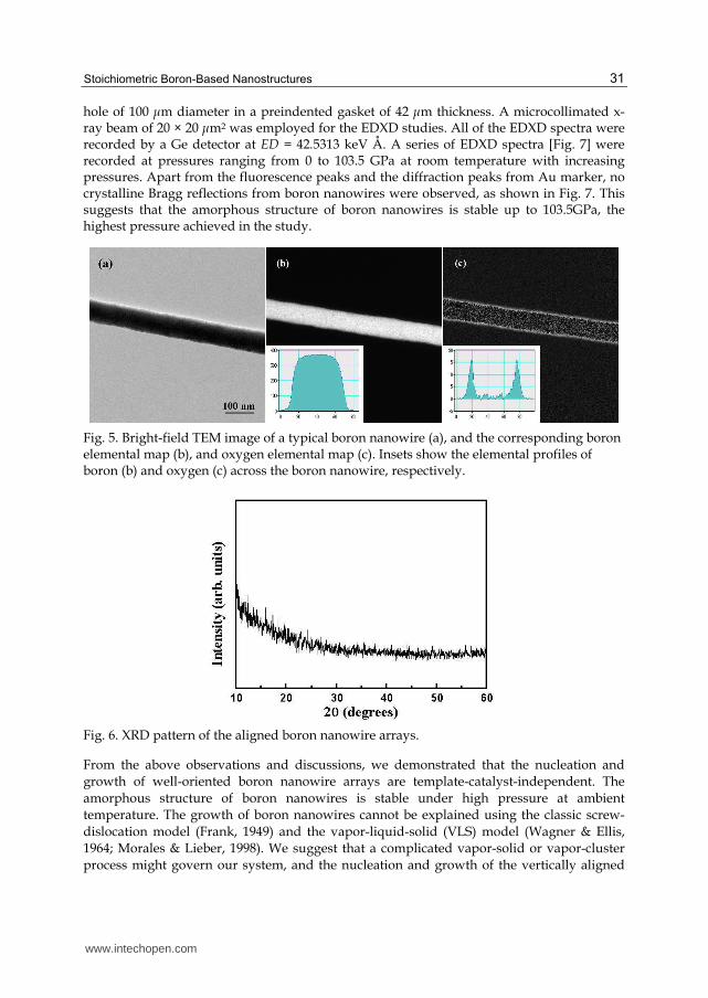
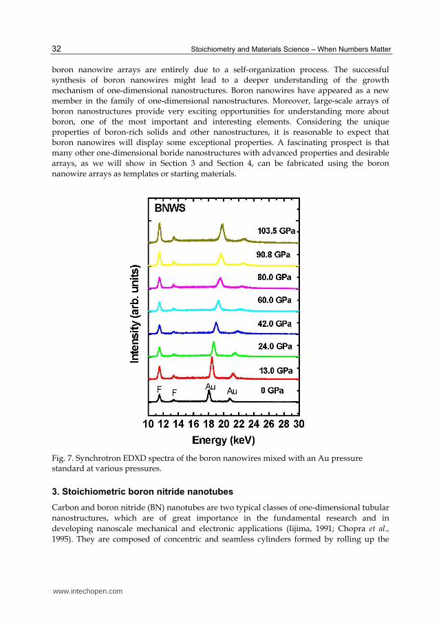
hole of 100 μm diameter in a preindented gasket of 42 μm thickness. A microcollimated x-ray beam of 20 × 20 μm2 was employed for the EDXD studies. All of the EDXD spectra were recorded by a Ge detector at ED = 42.5313 keV Å. A series of EDXD spectra [Fig. 7] were recorded at pressures ranging from 0 to 103.5 GPa at room temperature with increasing pressures. Apart from the fluorescence peaks and the diffraction peaks from Au marker, no crystalline Bragg reflections from boron nanowires were observed, as shown in Fig. 7. This suggests that the amorphous structure of boron nanowires is stable up to 103.5GPa, the highest pressure achieved in the study.
Fig. 5. Bright-field TEM image of a typical boron nanowire (a), and the corresponding boron elemental map (b), and oxygen elemental map (c). Insets show the elemental profiles of boron (b) and oxygen (c) across the boron nanowire, respectively.
Fig. 6. XRD pattern of the aligned boron nanowire arrays.
From the above observations and discussions, we demonstrated that the nucleation and growth of well-oriented boron nanowire arrays are template-catalyst-independent. The amorphous structure of boron nanowires is stable under high pressure at ambient temperature. The growth of boron nanowires cannot be explained using the classic screw-dislocation model (Frank, 1949) and the vapor-liquid-solid (VLS) model (Wagner & Ellis, 1964; Morales & Lieber, 1998). We suggest that a complicated vapor-solid or vapor-cluster process might govern our system, and the nucleation and growth of the vertically aligned
www.intechopen.com
Stoichiometry and Materials Science – When Numbers Matter
32
boron nanowire arrays are entirely due to a self-organization process. The successful synthesis of boron nanowires might lead to a deeper understanding of the growth mechanism of one-dimensional nanostructures. Boron nanowires have appeared as a new member in the family of one-dimensional nanostructures. Moreover, large-scale arrays of boron nanostructures provide very exciting opportunities for understanding more about boron, one of the most important and interesting elements. Considering the unique properties of boron-rich solids and other nanostructures, it is reasonable to expect that boron nanowires will display some exceptional properties. A fascinating prospect is that many other one-dimensional boride nanostructures with advanced properties and desirable arrays, as we will show in Section 3 and Section 4, can be fabricated using the boron nanowire arrays as templates or starting materials.
Fig. 7. Synchrotron EDXD spectra of the boron nanowires mixed with an Au pressure standard at various pressures.
3. Stoichiometric boron nitride nanotubes
Carbon and boron nitride (BN) nanotubes are two typical classes of one-dimensional tubular nanostructures, which are of great importance in the fundamental research and in developing nanoscale mechanical and electronic applications (Iijima, 1991; Chopra et al., 1995). They are composed of concentric and seamless cylinders formed by rolling up the
www.intechopen.com
Stoichiometric Boron-Based Nanostructures
33
planar atomic layers. Carbon nanotubes can be either metals or small gap semiconductors, depending on their diameter and chirality (Hamada et al., 1992; Saito et al., 1992; Dresselhaus et al., 1996). Boron nitride nanotubes, in contrast, are uniformly wide band-gap semiconductors having an energy gap independent of geometrical arrangements and wall number (Blase et al., 1994). Furthermore, BN nanotubes possess a higher resistance to oxidation at high temperature and have thermal conductivity comparable to carbon nanotubes (Xiao et al., 2004; Chang et al., 2005). Theoretical and experimental studies showed that the BN nanotubes possess the elastic modulus of 700-900 GPa, which is among the highest ones in one-dimensional fibers (Chopra & Zettl, 1998; Hernandez et al., 1998; Suryavanshi et al., 2004). These make BN nanostructures superior to carbon species in many mechanical and electronic applications, especially at high temperature.
To realize the practical applications of one-dimensional BN nanostructures in nanoscale electronic and mechanical devices, it is critically important to synthesize them in large quantities. However, so far the large scale synthesis of BN nanotubes and nanowires is still a challenging task. We have synthesized pure boron nanowires in high yield as described in Section 2. Can these novel nanowires be utilized as the starting materials for the creation of other boron-based nanostructures? Our research demonstrates that the answer to this question is an absolute YES. In this section, we describe the large quantity synthesis of pure BN nanotubes using a simple approach of annealing boron nanowire precursors in N2 atmosphere at 1500°C (Cao et al., 2007). The boron nanowire samples produced by magnetron sputtering were scraped from the substrates, packed into a Ta tube, and then placed in a home-made high temperature annealing furnace. After evacuating the furnace chamber to 10-5 Torr, high purity nitrogen gas was introduced into the chamber to a pressure of 150 Torr. The sample was heated to and kept at 1500 °C for 4 hours, and then cooled naturally to room temperature. After nitriding treatment, the nanowire product turns to gray-white from pitch black in color.
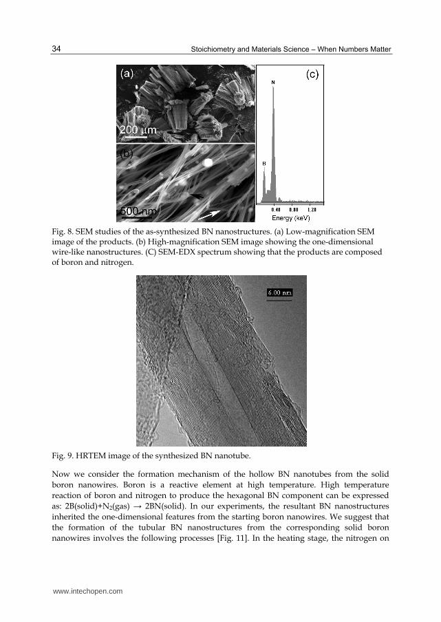
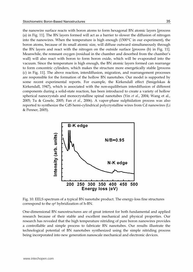
SEM studies show that the as-synthesized product consists of one dimensional nanostructures with uniform diameters [Fig. 8]. Energy-dispersive x-ray (EDX) [Fig. 8c] analysis revealed that the resulting nanostructures are composed of boron and nitrogen with B/N atomic ratio of approximately 1. This demonstrates clearly that the pure boron nanostructures have transformed into the corresponding nanoscale BN components by the high-temperature nitriding processing. TEM studies of the product show that the BN nanostructure has the typical tubular structure with a hollow core [Fig. 9]. The nanotube consists of concentric walls with an interlayer spacing of ~0.33 nm, being approximately the hexagonal BN (0002) interplanar distance. Our extensive TEM observations demonstrated that more than 80% of the synthesized BN nano-objects have cylindrical hollow cores with a high crystalline structure (the others are the porous BN nanowires with segmented voids in their interiors). The chemical stoichiometry of the individual nanostructures was further characterized using EELS. A typical EELS spectrum [Fig. 10] exhibits two distinct absorption features beginning at ~188 eV and ~398 eV. These correspond to the characteristic K-shell ionization edges for B and N, respectively. The fine structure of the B and N absorption edges in the spectrum reveals the sp2 bonding features between boron and nitrogen in the hexagonal BN (Chopra et al., 1995). The quantification analysis of the two edges gives the N/B atomic ratio of about 0.95±0.12, which is consistent with the BN stoichiometry.
www.intechopen.com
Stoichiometry and Materials Science – When Numbers Matter
34
Fig. 8. SEM studies of the as-synthesized BN nanostructures. (a) Low-magnification SEM image of the products. (b) High-magnification SEM image showing the one-dimensional wire-like nanostructures. (C) SEM-EDX spectrum showing that the products are composed of boron and nitrogen.
Fig. 9. HRTEM image of the synthesized BN nanotube.
Now we consider the formation mechanism of the hollow BN nanotubes from the solid boron nanowires. Boron is a reactive element at high temperature. High temperature reaction of boron and nitrogen to produce the hexagonal BN component can be expressed as: 2B(solid)+N2(gas) → 2BN(solid). In our experiments, the resultant BN nanostructures inherited the one-dimensional features from the starting boron nanowires. We suggest that the formation of the tubular BN nanostructures from the corresponding solid boron nanowires involves the following processes [Fig. 11]. In the heating stage, the nitrogen on
www.intechopen.com
Stoichiometric Boron-Based Nanostructures
35
the nanowire surface reacts with boron atoms to form hexagonal BN atomic layers [process (a) in Fig. 11]. The BN layers formed will act as a barrier to slower the diffusion of nitrogen into the nanowires. When the temperature is high enough (1500°C in our experiment), the boron atoms, because of its small atomic size, will diffuse outward simultaneously through the BN layers and react with the nitrogen on the outside surface [process (b) in Fig. 11]. Meanwhile, the remnant oxygen (residual in the chamber and desorbed from the chamber’s wall) will also react with boron to form boron oxide, which will be evaporated into the vacuum. Since the temperature is high enough, the BN atomic layers formed can rearrange to form concentric cylinders, which makes the structure more energetically stable [process (c) in Fig. 11]. The above reaction, interdiffusion, migration, and rearrangement processes are responsible for the formation of the hollow BN nanotubes. Our model is supported by some recent experimental reports. For example, the Kirkendall effect (Smigelskas & Kirkendall, 1947), which is associated with the non-equilibrium interdiffusion of different components during a solid-state reaction, has been introduced to create a variety of hollow spherical nanocrystals and monocrystalline spinal nanotubes (Yin et al., 2004; Wang et al., 2005; Tu & Gosele, 2005; Fan et al., 2006). A vapor-phase sulphidation process was also reported to synthesize the CdS hemi-cylindrical polycrystalline wires from Cd nanowires (Li & Penner, 2005).
Fig. 10. EELS spectrum of a typical BN nanotube product. The energy-loss fine structures correspond to the sp2 hybridization of h-BN.
One-dimensional BN nanostructures are of great interest for both fundamental and applied research because of their stable and excellent mechanical and physical properties. Our research has revealed that the high temperature nitriding of pure boron nanowires provides a controllable and simple process to fabricate BN nanotubes. Our results illustrate the technological potential of BN nanotubes synthesized using the simple nitriding process being incorporated into new generation nanoscale mechanical and electronic devices.
www.intechopen.com

Stoichiometry and Materials Science – When Numbers Matter
36
Fig. 11. Schematic diagram of the formation process of hollow BN nanotubes from solid boron nanowires.
4. Boron subnitride nanowires and heterostructured B6Nx/BN nanocables
One of the substantial challenges in developing nanotechnology is that new nanostructures need to be created and explored to serve as the functional units in the miniaturized nanosystems where high performance and reliability are required. Another practical challenge is that simple processes for reducing cost but improving efficiency are necessitated to mass-fabricate functional nanostructures at commercial scale. Boron and boron-rich borides are unique in terms of their novel structures and properties (Greenwood, 1973; Donohue, 1974; Matkovich, 1977; Emin, 1987; Albert & Hillebrecht, 2009). They provide an ideal platform to explore the fundamental natures in cluster physics and structural chemistry, thanks to the unusual three-center electron-deficient bond and most varied polymorphism existing in boron family. They possess many unrivalled properties ranging from superconducting metals to wide-band semiconductors, and are widely used in numerous technological applications, peculiarly in those where a refractory, light, and hard material is required (Greenwood, 1973; Donohue, 1974; Matkovich, 1977; Emin, 1987; Albert & Hillebrecht, 2009; Erements et al., 2001; Nagamatsu et al., 2001; Garvie et al., 1997; Hubert et al., 1997, 1998; He et al., 2002). For example, B6O possesses a hardness comparable with that of cubic BN, the second hardest material (Hubert et al., 1998; He et al., 2002); B6N shows a metal-like character in electron energy loss spectroscopy (EELS) studies (Garvie et al., 1997; Hubert et al., 1997). However, the syntheses of these useful boron-based materials normally
www.intechopen.com
Stoichiometric Boron-Based Nanostructures
37
require extreme high-pressure high-temperature conditions (Garvie et al., 1997; Hubert et al., 1997, 1998; He et al., 2002). Strategies to obtain these materials in useful shape-designed forms at ambient pressure are of practical importance for their technological applications.
In this section we present the creation of boron subnitride and B6Nx/BN radial heterostructured nanocables in bulk quantities using a simple process of nitriding the corresponding pure boron nanowires at 1200°C (Cao et al., 2008). The synthesized nanostructures consist of a core B6Nx nanowire with rhombohedral structure, a metastable high pressure phase, and a shell of hexagonal BN layers. This simple strategy might be used to rationally create other novel boron-based nanoheterostructures and nanocomposites in B-C-N-O system, and in principle, can provide nanoscale platforms to study high-pressure-induced phase transformation and reaction at ambient pressure.
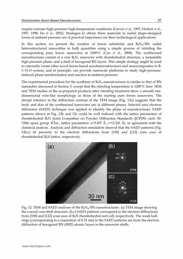
The experimental procedure for the synthesis of B6Nx nanostructures is similar to that of BN nanotubes discussed in Section 3, except that the nitriding temperature is 1200°C here. SEM and TEM studies of the as-prepared products after nitriding treatment show a smooth one-dimensional wire-like morphology as those of the starting pure boron nanowires. The abrupt interface in the diffraction contrast of the TEM image [Fig. 12a] suggests that the body and skin of the synthesized nanowires are of different phases. Selected area electron diffraction (SAED) technique was applied to identify the phase of nanostructures. SAED patterns shown in Fig. 12b and 12c could be well indexed with the lattice parameters of rhombohedral B6N (Joint Committee on Powder Diffraction Standards (JCPDS) card: 50-1504; space group R3m ; lattice parameters: a=5.457 Å, c=12.241 Å), in agreement with the chemical analysis. Analysis and diffraction simulation showed that the SAED patterns (Fig. 12b,c) fit precisely to the electron diffractions from [100] and [122] zone axes of rhombohedral B6N lattice, respectively.
Fig. 12. TEM and SAED analyses of the B6Nx/BN nanostructures. (a) TEM image showing the coaxial core-shell structure. (b,c) SAED patterns correspond to the electron diffractions from [100] and [122] zone axes of B6N rhombohedral unit cell, respectively. The weak half-rings (corresponding to a separation of 0.33 nm) in the SAED patterns are from the electron diffraction of hexagonal BN (0002) atomic layers in the nanowire shells.
www.intechopen.com

Stoichiometry and Materials Science – When Numbers Matter
38
HRTEM studies highlight that the smooth nanowires consist of a single-crystalline core sheathed with a few graphitic walls with an interlayer spacing of ~0.33 nm [Fig. 13]. The lattice images from the crystalline nanowire cores match the structure of rhombohedral B6N. The shell layers can be designated to hexagonal BN (0002) planes based on chemical analysis (see below) and TEM studies.
Fig. 13. HRTEM image of the B6Nx/BN nanostructures. The longitudinal axis of the nanowire orientate roughly along the [241] direction.
We used EDX and EELS to characterize the chemical stoichiometry of the nanostructures. The EDS spectrum revealed that the nanostructures contain boron and nitrogen; the N:B atomic ratio was quantified to be about 1:4.8. Figure 14a shows a representative EELS spectrum taken from the central part of a typical nanowire. Because the shell layers are very thin (2-4 nm), the EELS signals are mainly from the core phase. EELS spectrum presents two sharp threshold peaks beginning at ~185 eV and ~396 eV, corresponding to the characteristic K-shell ionization edges for B and N, respectively. EELS quantification of the spectra gives the N/B atomic ratio of about 0.21±0.034, which is in good agreement with the EDX analysis. We also acquired EELS spectra from pure α-rhombohedral boron and hexagonal BN nanotube for a comparison [see Fig. 14b and 14c]. The fine structures of boron K-edges from the product nanowires show a similarity to those from bulk pure boron (B K-edges typical of icosahedral rhombohedral boron-rich phases), but a distinguishing difference from those of hexagonal BN. Our results are coincident with previous EELS studies of the B6N and other icosahedral boron-rich phases (Garvie et al., 1997).
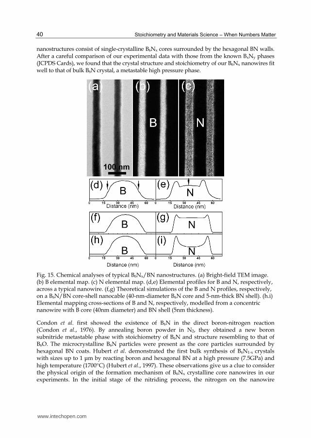
We acquired the elemental mapping of B and N in the produced BNx nanostructures. Figure 15a-c shows the bright field TEM image and the corresponding energy-filtered images of two typical BNx nanostructures. The B elemental map, shown clearly in Fig. 15b, has uniformly bright contrast in the core throughout the nanowires. Careful observations reveal a reduced intensity at the peripheries of the nanowires in the B map. This suggests that the nanowire shells are boron-deficient compared to the core region where the distribution of B is homogeneous. In contrast, the N elemental map [Fig. 15c] shows a bright contrast sheath and a dark core with much lower brightness, indicating that the coating is nitrogen-rich.
www.intechopen.com

Stoichiometric Boron-Based Nanostructures
39
Fig. 14. EELS spectra of B6Nx nanowire (a), bulk pure α-boron (b), and BN nanotube (c). The B K edge features from B6Nx nanowire are similar to that from bulk pure boron, but are obviously different from that of BN. The insets show the magnified features of the B and N K-edges from B6Nx nanostructure (a), pure boron (b), and BN (c).
Linescan analyses of the elemental distributions across the nanowire in the B and N maps show a hill-shaped B concentration profile and valley-like N profile [Fig. 15d,e], confirming that our BNx nanostructures have a nitrogen-rich shell, and is in good agreement with the conclusion that the nanowire sheath is hexagonal BN. The chemical profiles of B and N, as shown in Figure 15d,e, also highlight two interesting features. First, two shoulder peaks (indicated by the arrows in Fig. 15d) exist in both sides of the B concentration profile. Second, the valley in the intensity profile of the N distribution has a protruding central section (indicated by the arrow in Fig. 15e). Considering that the total N/B atomic ratio in the products is about 1:5, and the BN shell has a higher N/B ratio of 1:1, we can conclude that the core of the synthesized nanostructure has a nominal stoichiometry of B6Nx (x<1.2). To confirm this assignment, we performed theoretical simulation of the cross-sectional elemental mapping of B and N in the synthetic concentric cylinders of B6N/BN and B/BN. Figure 15f,g shows the calculated elemental profiles in the B6N/BN core-shell nanowire with a 40-nm-diameter core and 5-nm-thick shell. The fine features of the calculated B and N mapping cross-sections are in good agreement with the experimental data. In contrast, the theoretical cross-section N profile in the B/BN nanostructure (a 40-nm-diameter B core with a 5-nm-thick BN shell) shows a central dip in the N valley (Fig. 15i), which differs distinctly from the experimental results [Fig. 15e]. Taken together, these structure and composition data show that the produced
www.intechopen.com
Stoichiometry and Materials Science – When Numbers Matter
40
nanostructures consist of single-crystalline B6Nx cores surrounded by the hexagonal BN walls. After a careful comparison of our experimental data with those from the known BxNy phases (JCPDS Cards), we found that the crystal structure and stoichiometry of our B6Nx nanowires fit well to that of bulk B6N crystal, a metastable high pressure phase.
Fig. 15. Chemical analyses of typical B6Nx/BN nanostructures. (a) Bright-field TEM image. (b) B elemental map. (c) N elemental map. (d,e) Elemental profiles for B and N, respectively, across a typical nanowire. (f,g) Theoretical simulations of the B and N profiles, respectively, on a B6N/BN core-shell nanocable (40-nm-diameter B6N core and 5-nm-thick BN shell). (h.i) Elemental mapping cross-sections of B and N, respectively, modelled from a concentric nanowire with B core (40nm diameter) and BN shell (5nm thickness).
Condon et al. first showed the existence of B6N in the direct boron-nitrogen reaction (Condon et al., 1976). By annealing boron powder in N2, they obtained a new boron subnitride metastable phase with stoichiometry of B6N and structure resembling to that of B6O. The microcrystalline B6N particles were present as the core particles surrounded by hexagonal BN coats. Hubert et al. demonstrated the first bulk synthesis of B6N1-x crystals with sizes up to 1 μm by reacting boron and hexagonal BN at a high pressure (7.5GPa) and high temperature (1700°C) (Hubert et al., 1997). These observations give us a clue to consider the physical origin of the formation mechanism of B6Nx crystalline core nanowires in our experiments. In the initial stage of the nitriding process, the nitrogen on the nanowire
www.intechopen.com

Stoichiometric Boron-Based Nanostructures
41
surface reacts with boron atoms to form fragments of BN atomic layers according to the reaction 2B(solid)+N2(gas)→2BN(solid). As the reaction proceeding, the BN fragments on the outer surface wrap around the host nanowire to form a nano-capsule structure. At high temperature, the B and N atoms in the BN layers can rearrange and the BN fragments interconnect to form perfect concentric cylinders, which makes the structure more energetically stable. Thus the diameter of the BN capsule tends to shrink, and a pressure will build up inside the BN vessel. The BN sheath also separates the residual nanowire from the N2 atmosphere, and prevents the inward diffusion of N atoms into the nanowire. The BN nano-capsule formed thus acts as a high pressure cell to promote the reaction 12B+N2 →B6N. Under these conditions, the residual core nanowires inside the BN shells reacts with N atoms to form B6Nx nanostructures with the assistance of high-pressure build-up in the nanocells. As a result, the heterostructured B6Nx/BN nanocables are formed. In this model, the isolated high-pressure BN cell and lower inward migration of nitrogen atoms are responsible for the high-pressure-induced formation of nano-crystalline B6Nx phase. The temperature also takes a critical role in our experiments. At a higher nitriding temperature of 1500°C, all the pure boron precursors were transformed into BN nanotubes (Cao et al., 2007). The nitriding temperature of 1200°C made for the formation of B6Nx/BN core-shell nanostructure, suggesting that B6Nx phase inside the BN nanocell is thermodynamically stable at this temperature. Banhart and Ajayan revealed that carbon onions can act as nanoscopic pressure cells for diamond nucleation and growth in the cores of carbon onions under high temperature and electron irradiation conditions (Banhart & Ajayan, 1996). Golberg and coworkers demonstrated the formation of solid nitrogen inside the BN nanocages, a structural analog of carbon onions, due to the existence of super-high-pressure inside them (Golberg et al., 2002). They also observed the high-pressure-induced phase transformation of hexagonal BN to cubic BN inside the BN high-pressure nanocells. Multiwalled carbon nanotubes as high-pressure cylinders and nanoextruders were also reported to deform, extrude, and break hard nanomaterials that are encapsulated inside the core (Sun et al., 2006). All of these experimental observations support our conclusion on the nanocell-high-pressure-assisted formation mechanism of B6Nx/BN nanostructures in the nitriding reaction.
It is reasonable to expect that the B6N nanostructures should share some of the very interesting physical and chemical properties with other boron-rich solids, e.g., low density, high hardness, chemical inertness, unique mechanical, thermal, and electronic properties, etc. The coaxial B6N/BN nanocable heterostructures are of importance as the promising building blocks in developing nanoscale devices and nano-composites. Our research suggests that the BN nanocells in a similar process can be used as a template to study the pressure-induced phase transformation at nanoscale as well as to synthesize other unique boron-based nanostructures that cannot be formed under normal conditions. This simple synthetic strategy may be used as a general approach for the bulk-fabrication of a variety of intriguing boron-based nanocomposites and nanoheterostructures in B-C-N-O system, through rationally optimizing the synthetic conditions and utilizing the nanocell high-pressure effect.
5. Summary and outlook
In this Chapter, we describe mainly the investigations from our laboratory directed toward the synthesis of stoichiometric boron-based nanostructures. Our goal has been to create new boron and boride nanostructures with advanced properties and desired dimensionality. Through a detailed investigation on the structures and properties of new boron-based nanomaterials, we
www.intechopen.com

Stoichiometry and Materials Science – When Numbers Matter
42
target at advancing our understanding of the unique boron chemistry and physics in the nanoscale regime. Another goal of our research has been to develop simple and cost-effective methods for mass-fabricating boron-based nanostructures and their highly ordered arrays in order to facilitate their practical applications in nanoscale devices and nano-composites.
We have synthesized large-area arrays of well-aligned boron nanowires using the simple approach of magnetron sputtering. Our research suggests that the magnetron sputtering approach, which is widely used in the preparation of films and multilayers in both industry and academia, can be employed as a general method for synthesis of some nanometer-sized materials with desirable dimensionalities and ordered assemblies via the rational design of the targets and the proper control of the experimental conditions. We have synthesized high-concentration nitrogen-doped carbon nanotube using magnetron sputtering of a mixture of nanometre-sized graphite and nickel powders in a nitrogen atmosphere (Cao et al., 2003).
Using these boron nanostructures as the starting materials, we have created highly pure BN nanotubes in large quantities and B6Nx/BN radial heterostructured nanocables in high yield by annealing pure boron nanowire precursors in N2 atmosphere at 1500°C and 1200°C, respectively. Through exploiting the annealing variations in the simple nitriding process, we can expect to tune the properties of the BN nanostructures via the chemical modulation, and to extend this simple process for bulk fabrication of a wealth of boron-based nanoheterostructures and nanocomposites in B-C-N-O system. Our results show promising technological potential of fabricating new and hybrid boron-based nanostructures using simple processes for practical applications.
We believe there is a promising bright future in science and technology for boron and boride nanostructures. Theoretical studies suggest the existence of new boron-based materials showing at least the same variety of nanoscale forms and interesting properties as those known for carbon. Besides the boron nanotubes, theoretical AlB2 nanotubes show a metallic density of states, independent of their chirality (Quandt et al., 2001); nanotubular B2O and BeB2, are new semiconductors and metals in one dimension (Zhang & Crespi, 2002). Theoretical calculations show that these new classes of tubular structures promise to offer properties unavailable to the previously studied C, B, B-C-N, and B-N based systems. As for boron cage-like nanostructures, Szwacki and coworkers predicted using ab initio calculations that B80, which is very similar in shape and symmetry to the carbon fullerene C60, is an energetically stable boron fullerene (Szwacki et al., 2007). However, the synthesis of these theoretical novel boron-based nanostructures remains a challenge. Though Ciuparu et al. claimed that they have synthesized pure boron single-wall nanotubes (Ciuparu et al., 2004), no any subsequent work has come out following their result since it was published. There remain many fundamental and practical issues about the structures and properties of boron-based nanostructures that deserve future explorations. We expect that the investigations on boron-based nanostructures will provide new insights into boron chemistry and physics, and boron nanostructures will serve as important building blocks for nanotechnology.
6. Acknowledgment
We thank our coworkers who have made contributions to the work described in this chapter, including Ze Zhang, He Tian, Meng He, Chunxiao Gao, Yiqian Wang, Yanchun Li, Jing Liu, Jun Zhang, K. Hahn, and C. Scheu. We would like to acknowledge the Natural Science Foundation of China for financial support.
www.intechopen.com
Stoichiometric Boron-Based Nanostructures
43
7. References
Ajayan, P.M. & Ebbesen, T.W. (1997). Nanometre-size Tubes of Carbon. Reports on Progress in Physics, Vol. 60, No. 10, (October 1997), pp. 1025-1062, ISSN 0034-4885
Albert, B. & Hillebrecht, H. (2009). Boron: Elementary Challenge for Experimenters and Theoreticians. Angew. Chem. Int. Ed., Vol. 48, No. 46, (November 2009), pp8640–8668, ISSN: 1433-7851
Banhart, F. & Ajayan, P.M. (1996). Carbon Onions as Nanoscopic Pressure Cells for Diamond Formation. Nature, Vol. 382, No. 6590, (August 1996), pp. 433-435, ISSN 0028-0836
Blase, X.; Rubio, A.; Louie, S.G. & Cohen, M.L. (1994). Stability and Band Gap Constancy of Boron-Nitride Nanotubes. Europhysics Letters, Vol. 28, No. 5, (November 1994), pp. 335-340, ISSN 0295-5075
Boustani, I.; Quandt, A.; Hernandez, E. & Rubio, A. (1999). New Boron Based Nanostructured Materials. Journal of Chemical Physics, Vol. 110, No. 6, (February 1999), pp. 3176-3185, ISSN 0021-9606
Boustani, I.; Quandt, A. & Rubio A. (2000). Boron Quasicrystals and Boron Nanotubes: Ab Initio Study of Various B96 Isomers. Journal of Solid State Chemistry, Vol. 154, No. 1, (October 2000), pp. 269-274, ISSN 0022-4596
Cao, L.M.; Zhang, Z.; Sun, L.L.; Gao, C.X.; He, M.; Wang, Y.Q.; Li, Y.C.; Zhang, X.Y.; Li, G.; Zhang, J. & Wang, W.K. (2001). Well-Aligned Boron Nanowire Arrays. Advanced Materials, Vol. 13, No. 22, (November 2001), pp. 1701-1704, ISSN 0935-9648
Cao, L.M.; Hahn, K.; Scheu, C.; Ruhle, M.; Wang, Y.Q.; Zhang, Z.; Gao, C.X.; Li, Y.C.; Zhang, X.Y.; He, M.; Sun, L.L. & Wang, W.K. (2002). Template-Catalyst-Free Growth of Highly Ordered Boron Nanowire Arrays. Applied Physics Letters, Vol. 80, No. 22, (June 2002), pp. 4226-4228, ISSN 0003-6951
Cao, L.M.; Liu, J.; Gao, C.X.; Li, Y.C.; Li, X.D.; Wang, Y.Q. Wang, Y.Q.; Zhang, Z.; Cui, Q.L.; Zou, G.T.; Sun, L.L. & Wang, W.K. (2002). Synthesis of Well-Aligned Boron Nanowires and Their Structural Stability under High Pressure. Journal of Physics-Condensed Matter, Vol. 14, No. 44, (November 2002), pp. 11017-11021, ISSN 0953-8984
Cao, L.M.; Zhang, X.Y.; Gao, C.X.; Wang, W.K.; Zhang, Z.L. & Zhang, Z. (2003). High-Concentration Nitrogen-Doped Carbon Nanotube Arrays. Nanotechnology, Vol. 14, No. 8, (August 2003), pp. 931-934, ISSN 0957-4484
Cao, L.M.; Zhang, X.Y.; Tian, H.; Zhang, Z. & Wang, W.K. (2007). Boron Nitride Nanotube Branched Nanojunctions. Nanotechnology, Vol. 18, No. 15, (April 2007), pp. 155605(1-4), ISSN: 0957-4484
Cao, L.M.; Tian, H.; Zhang, Z.; Feng, M.; Zhan, Z.J.; Wang, W.K. & Zhang, X.Y. (2008). Heterostructured B6Nx/BN Nanocable and Nanofeather Nanojunctions. Crystal Growth & Design, Vol. 8, No. 12, (December 2008), pp: 4350-4354, ISSN 1528-7483
Chang, C.W.; Han, W.Q. & Zettl, A. (2005). Thermal Conductivity of B-C-N and BN Nanotubes. Applied Physics Letters, Vol. 86, No. 17, (April 2005), pp. 173102(1-3), ISSN 0003-6951
Chopra, N.G.; Luyken, R.J.; Cherrey, K.; Crespi, V.H.; Cohen, M.L.; Louie, S.G. &Zettl, A. (1995). Boron-Nitride Nnanotubes. Science, Vol. 269, No. 5226, (August 1995), pp. 966-967, ISSN 0036-8075
Chopra, N.G. & Zettl, A. (1998). Measurement of the Elastic Modulus of a Multi-Wall Boron Nitride Nanotube. Solid State Communications, Vol. 105, No. 5, (February 1998), pp. 297-300, ISSN 0038-1098
Ciuparu, D.; Klie, R.F.; Zhu, Y.M. & Pfefferle, L. (2004). Synthesis of Pure Boron Single-Wall Nanotubes. Journal of Physical Chemistry B, Vol. 108, No. 13, (April 2004), pp. 3967-3969, ISSN 1520-6106
www.intechopen.com

Stoichiometry and Materials Science – When Numbers Matter
44
Condon, J.B.; Holcombe, C.E.; Johnson, D.H. & Steckel, L.M. (1976). The Kinetics of the Boron Plus Nitrogen Reaction. Inorganic Chemistry, Vol. 15, No. 9, (September 1976), pp. 2173-2179, ISSN 0020-1669
Donohue, J. (1974). The Structures of the Elements, pp. 48-83, Wiley, ISBN 0471217883, New York
Dresselhaus, M.S.; Dresselhaus, G. & Ecklund, P.C. (1996). Science of Fullerenes and Carbon Nanotubes: Their Properties and Applications, Academic, ISBN 0122218205, New York
Emin, D. (1987). Icosahedral Boron-Rich Solids. Physics Today, Vol. 40, No. 1, (January 1987), pp. 55-62, ISSN 0031-9228
Eremets, M.I.; Struzhkin, V.V.; Mao, H.K. & Hemley, R.J. (2001). Superconductivity in Boron. Science, Vol. 293, No.5528, (July 2001), pp. 272-274, ISSN 0036-8075
Fan, H.J.; Knez, M.; Scholz, R.; Nielsch, K.; Pippel, E.; Hesse, D.; Zacharias, M. & Gosele, U. (2006). Monocrystalline Spinel Nanotube Fabrication Based on the Kirkendall Effect. Nature Materials, Vol. 5, No. 8, (August 2006), pp. 627-631, ISSN 1476-1122
Frank, F.C. (1949). The Infulence of Dislocations on Crystal Growth. Discussions of the Faraday Society, No. 5, (1949), pp. 48-54. IDS Number: UL198
Fujimori, M.; Nakata, T.; Nakayama, T.; Nishibori, E.; Kimura, K.; Takata, M. & Sakata, M. (1999). Peculiar Covalent Bonds in a-Rhombohedral Boron. Physical Review Letters, Vol. 82, No. 22, (May 1999), pp. 4452-4455, ISSN 0031-9007
Garvie, L.A.J.; Hubert, H.; Petuskey, W.T.; McMillan, P.F. & Buseck, P.R. (1997), High-Pressure, High-Temperature Syntheses in the B-C-N-O System - II. Electron Energy-Loss Spectroscopy (EELS). Journal of Solid State Chemistry, Vol. 133, No. 2, (November 1997), pp. 365-371, ISSN 0022-4596
Gindulyte, A.; Lipscomb, W.N. & Massa, L. (1998). Proposed Boron Nanotubes. Inorganic Chemistry, Vol. 37, No. 25, (December 1998), pp. 6544-6545, ISSN 0020-1669
Gindulyte, A.; Krishnamachari, N.; Lipscomb, W.N. & Massa, L. (1998). Quantum Chemical Calculations of Proposed Multicage Boron Fullerenes. Inorganic Chemistry, Vol. 37, No. 25, (December 1998), pp. 6546-6548, ISSN 0020-1669
Golberg, D.; Bando, Y.; Sato, T.; Grobert, N.; Reyes-Reyes, M.; Terrones, H. & Terrones, M. (2002). Nanocages of Layered BN: Super-High-Pressure Nanocells for Formation of Solid Nitrogen. Journal of Chemical Physics, Vol. 116, No. 19, (May 2002), pp. 8523-8532, ISSN 0021-9606
Greenwood, N. N. (1973). In: Comprehensive Inorganic Chemistry, J. C. Bailar Jr., H. J. Emeléus, Sir R. Nyholm, A. F. Trotman-Dickenson, (Eds.), Pergamon, Vol. 1, pp. 665-991, ISBN 0080169899, Oxford
Hamada, N.; Sawada, S. & Oshiyama, A. (1992). New One-Dimensional Conductors – Graphitic Microtubules. Physical Review Letters, Vol. 68, No. 10, (March 1992), pp. 1579-1581, ISSN 0031-9007
He, D.W.; Zhao, Y.S.; Daemen, L.; Qian, J.; Shen, T.D. & Zerda, T.W. (2002). Boron Suboxide: As Hard as Cubic Boron Nitride. Applied Physics Letters, Vol. 81, No. 4, (July 2002), pp. 643-645, ISSN 0003-6951
Hernandez, E.; Goze, C.; Bernier, P. & Rubio, A. (1998). Elastic Properties of C and BxCyNz Composite Nanotubes. Physical Review Letters, Vol. 80, No. 20, (May 1998), pp. 4502-4505, ISSN 0031-9007
Hu, J.T.; Odom, T.W. & Lieber, C.M. (1999). Chemistry and Physics in One Dimension: Synthesis and Properties of Nanowires and Nanotubes. Accounts of Chemical Research, Vol. 32, No. 5, (May 1999), pp. 435-445, ISSN 0001-4842
www.intechopen.com

Stoichiometric Boron-Based Nanostructures
45
Hubert, H.; Garvie, L.A.J.; Buseck, P.R.; Petuskey, W.T. & McMillan, P.F. (1997). High-Pressure, High-Temperature Syntheses in the B-C-N-O System - I. Preparation and Characterization. Journal of Solid State Chemistry, Vol. 133, No. 2, (November 1997), pp. 356-364, ISSN 0022-4596
Hubert, H.; Devouard, B.; Garvie, L.A.J.; O'Keeffe, M.; Buseck, P.R.; Petuskey, W.T. & McMillan, P.F. (1998). Icosahedral Packing of B12 Icosahedra in Boron Suboxide (B6O). Nature, Vol. 391, No. 6665, (January 1998), pp. 376-378, ISSN 0028-0836
Iijima, S. (1991). Helical Microtubules of Graphitic Carbon. Nature, Vol. 354, No. 6348, (November 1991), pp. 56-58, ISSN: 0028-0836
Kirihara, K.; Hyodo, H.; Fujihisa, H.; Wang, Z.; Kawaguchi, K.; Shimizu, Y.; Sasaki, T.; Koshizaki, N.; Soga, K. & Kimura, K. (2006). Mg-Doping Experiment and Electrical Transport Measurement of Noron Nanobelts. Journal of Solid State Chemistry, Vol. 179, No. 9, (September 2006), pp. 2799-2804, ISSN: 0022-4596
Kroto, H.W.; Heath, J.R.; O'Brien, S.C.; Curl R.F. & Smalley, R. E. (1985). C60: Buckminsterfullerene. Nature, Vol. 318, No. 6042, (November 1985), pp. 162-163, ISSN: 0028-0836
Kuchibhatla, S.V.N.T.; Karakoti, A.S.; Bera, D. & Seal, S. (2007). One Dimensional Nanostructured Materials. Progress in Materials Science, Vol. 52, No. 5, (July 2007), pp. 699-913, ISSN 0079-6425
Li, Q.G. & Penner, R.M. (2005). Photoconductive Cadmium Sulfide Hemicylindrical Shell Nanowire Ensembles. Nano Letters, Vol. 5, No. 9, (September 2005), pp. 1720-1725, ISSN 1530-6984
Liu, F.; Tian, J.F.; Bao, L.H.; Yang, T.Z.; Shen, C.M.; Lai, X.Y.; Xiao, Z.M.; Xie, W.G.; Deng, S.Z.; Chen, J.; She, J.C.; Xu, N.S. & Gao, H.J. (2008). Fabrication of Vertically Aligned Single-Crystalline Boron Nanowire Arrays and Investigation of Their Field-Emission Behavior. Advanced Materials, Vol. 20, No. 13, (July 2008), pp. 2609-2615, ISSN: 0935-9648
Matkovich, V.I. (Ed.). (1977). Boron and Refractory Borides, Springer, ISBN 038708181X, New York Meng, X.M.; Hu, J.Q.; Jiang, Y.; Lee, C.S. & Lee, S.T. (2003). Boron Nanowires Synthesized by
Laser Ablation at High Temperature. Chemical Physics Letters, Vol. 370, No. 5-6, (May 2003), pp. 825-828, ISSN: 0009-2614
Morales, A.M. & Lieber, C.M. (1998). A laser ablation method for the synthesis of crystalline semiconductor nanowires. Science, Vol. 279, No. 5348, (January 1998), pp. 208-211, ISSN 0036-8075
Nagamatsu, J.; Nakagawa, N.; Muranaka, T.; Zenitani, Y. & Akimitsu, J. (2001). Superconductivity at 39 K in Magnesium Diboride. Nature, Vol. 410, No. 6824, (March 2001), pp. 63-64, ISSN 0028-0836
Nelmes, R.J.; Loveday, J.S.; Wilson, R.M.; Marshall, W.G.; Besson, J.M.; Klotz, S.; Hamel, G.; Aselage, T.L. & Hull, S. (1995). Observation of Inverted-Molecular Compression in Boron Carbide. Physical Review Letters, Vol. 74, No. 12, (March 1995), pp. 2268-2271, ISSN 0031-9007
Otten, C.J.; Lourie, O.R.; Yu, M.F.; Cowley, J.M.; Dyer, M.J.; Ruoff, R.S. & Buhro, W.E. (2002). Crystalline Boron Nanowires. Journal of the American Chemical Society, Vol. 124, No. 17, (May 2002), pp. 4564-4565, ISSN 0002-7863
Quandt, A. & Boustani, I. (2005). Boron Nanotubes. CHEMPHYSCHEM, Vol. 6, No. 10, (October 2005), pp. 2001-2008, ISSN 1439-4235
Quandt, A.; Liu, A.Y. & Boustani, I. (2001). Density-Functional Calculations for Prototype Metal-Boron Nanotubes. Physical Review B, Vol. 64, No. 12, (September 2001), pp. 125422 (1-5), ISSN 1098-0121
www.intechopen.com
Stoichiometry and Materials Science – When Numbers Matter
46
Saito, R.; Fujita, M.; Dresselhaus, G.; Dresselhaus, M.S. (1992). Electronic Structure of Graphene Tubules Based C60. Physical Review B. Vol. 46, No. 3, (July 1992), pp. 1804-1811, ISSN 0163-1829
Smigelskas, A.D. & Kirkendall, E.O. (1947). Zinc Diffusion in Alpha-Brass. Transactions of the American Institute of Mining and Metallurgical Engineers, Vol. 171, (1947), pp. 130-142, IDS No. XR336
Sun, L.; Banhart, F.; Krasheninnikov, A.V.; Rodriguez-Manzo, J.A.; Terrones, M. & Ajayan, P.M. (2006). Carbon Nanotubes as High-Pressure Cylinders and Nanoextruders. Science, Vol. 312, No. 5777, (May 2006), pp. 1199-1202, ISSN 0036-8075
Suryavanshi, A.P.; Yu, M.F.; Wen, J.G.; Tang, C.C. & Bando, Y. (2004). Elastic Modulus and Resonance Behavior of Boron Nitride Nanotubes. Applied Physics Letters, Vol. 84, No. 14, (April 2004), pp. 2527-2529, ISSN 0003-6951
Szwacki, N.G.; Sadrzadeh, A. & Yakobson, B.I. (2007). B80 Fullerene: An ab initio Prediction of Geometry, Stability, and Electronic Structure. Physical Review Letters, Vol. 98, No. 16, (April 2007), pp. 166804(1-4), ISSN 0031-9007
Tu, K.N. & Gosele, U. (2005). Hollow Nanostructures Based on the Kirkendall Effect: Design and Stability Considerations. Applied Physics Letters, Vol. 86, No. 9, (February 2005), pp. 093111(1-3), ISSN 0003-6951
Vast, N.; Baroni, S.; Zerah, G.; Besson, J.M.; Polian, A.; Grimsditch, M. & Chervin, J.C. (1997). Lattice Dynamics of Icosahedral Alpha-Boron Under Pressure. Physical Review Letters, Vol. 78, No. 4, (January 1997), pp. 693-696, ISSN 0031-9007
Wang, Y.L.; Cai, L. & Xia, Y.N. (2005). Monodisperse Spherical Colloids of Pb and Their Use as Chemical Templates to Produce Hollow Particles. Advanced Materials, Vol. 17, No. 4, (February 2005), pp. 473-477, ISSN 0935-9648
Wang, Z.K.; Shimizu, Y.; Sasaki, T.; Kawaguchi, K.; Kimura, K. & Koshizaki, N. (2003). Catalyst-Free Fabrication of Single Crystalline Boron Nanobelts by Laser Ablation. Chemical Physics Letters, Vol. 368, No. 5-6, (January 2003), pp. 663-667, ISSN: 0009-2614
Wagner, R.S. & Ellis, W. C. (1964). Vapor-Liquid-Solid Mechanism of Single Crystal Growth. Applied Physics Letters, Vol. 4, No. 5, (March 1964), pp. 89-90, ISSN 0003-6951
Wu, Y.Y.; Messer, B.& Yang, P.D. (2001). Superconducting MgB2 Nanowires. Advanced Materials, Vol. 13 No. 19, (October 2001), pp. 1487-1489, ISSN: 0935-9648
Xiao, Y.; Yan, X.H.; Cao, J.X.; Ding, J.W.; Mao, Y.L. & Xiang, J. (2004). Specific Heat and Quantized Thermal Conductance of Single-Walled Boron Nitride Nanotubes. Physical Review B, Vol. 69, No. 20, (May 2004), pp. 205415(1-5), ISSN 1098-0121
Xu, T.T.; Zheng, J.G.; Wu, N.; Nicholls, A.W.; Roth, J.R.; Dikin, D.A. & Ruoff, R.S. (2004). Crystalline Boron Nanoribbons: Synthesis and Characterization. Nano Letters, Vol. 4, No. 5, (April 2004), pp. 963-968, ISSN 1530-6984
Yin, Y.D.; Rioux, R.M.; Erdonmez, C.K.; Hughes, S.; Somorjai, G.A. & Alivisatos, A.P. (2004). Formation of Hollow Nanocrystals through the Nanoscale Kirkendall Effect. Science, Vol. 304, No. 5671, (April 2004), pp. 711-714, SSN 0036-8075
Yun, S.H.; Wu, J.Z.; Dibos, A.; Gao, X. & Karlsson, U.O. (2005). Growth of Inclined Boron nanowire Bundle Arrays in an Oxide-Assisted Vapor-Liquid-Solid Process. Applied Physics Letters, Vo. 87, No. 11, (september 2005), pp. 113109 (1-3), ISSN 0003-6951
Zhang, P.H. & Crespi, V.H. (2002). Theory of B2O and BeB2 Nanotubes: New Semiconductors and Metals in One Dimension. Physical Review Letters, Vol. 89, No. 5, (July 2002), pp. 056403(1-4), ISSN 0031-9007
Zhang, Y.J.; Ago, H.; Yumura, M.; Komatsu, T.; Ohshima, S.; Uchida, K. & Iijima, S. (2002). Synthesis of Crystalline Boron Nanowires by Laser Ablation. Chemical Communications, No. 23, (October 2002), pp. 2806-2807, ISSN 1359-7345
www.intechopen.com
Stoichiometry and Materials Science - When Numbers MatterEdited by Dr. Alessio Innocenti
ISBN 978-953-51-0512-1Hard cover, 436 pagesPublisher InTechPublished online 11, April, 2012Published in print edition April, 2012
InTech EuropeUniversity Campus STeP Ri Slavka Krautzeka 83/A 51000 Rijeka, Croatia Phone: +385 (51) 770 447 Fax: +385 (51) 686 166www.intechopen.com
InTech ChinaUnit 405, Office Block, Hotel Equatorial Shanghai No.65, Yan An Road (West), Shanghai, 200040, China
Phone: +86-21-62489820 Fax: +86-21-62489821
The aim of this book is to provide an overview on the importance of stoichiometry in the materials science field.It presents a collection of selected research articles and reviews providing up-to-date information related tostoichiometry at various levels. Being materials science an interdisciplinary area, the book has been divided inmultiple sections, each for a specific field of applications. The first two sections introduce the role ofstoichiometry in nanotechnology and defect chemistry, providing examples of state-of-the-art technologies.Section three and four are focused on intermetallic compounds and metal oxides. Section five describes theimportance of stoichiometry in electrochemical applications. In section six new strategies for solid phasesynthesis are reported, while a cross sectional approach to the influence of stoichiometry in energy productionis the topic of the last section. Though specifically addressed to readers with a background in physical science,I believe this book will be of interest to researchers working in materials science, engineering and technology.
How to referenceIn order to correctly reference this scholarly work, feel free to copy and paste the following:
Limin Cao, Xiangyi Zhang, Wenkui Wang and Min Feng (2012). Stoichiometric Boron-Based Nanostructures,Stoichiometry and Materials Science - When Numbers Matter, Dr. Alessio Innocenti (Ed.), ISBN: 978-953-51-0512-1, InTech, Available from: http://www.intechopen.com/books/stoichiometry-and-materials-science-when-numbers-matter/stoichiometric-boron-based-nanostructures

© 2012 The Author(s). Licensee IntechOpen. This is an open access articledistributed under the terms of the Creative Commons Attribution 3.0License, which permits unrestricted use, distribution, and reproduction inany medium, provided the original work is properly cited.