Stanford University Concurrent VLSI Architecture Group ...
26
Stanford University Concurrent VLSI Architecture Group Memo 126 Maximizing the Filter Rate of L0 Compiler-Managed Instruction Stores by Pinning Jongsoo Park, James Balfour and William J. Dally Concurrent VLSI Architecture Group Computer Systems Laboratory Stanford University, Stanford, CA 94305 Email: {jongsoo,jbalfour,dally}@cva.stanford.edu September 29, 2009 Abstract We present an allocation algorithm for small L0 compiler-managed instruction stores (cmiss) that significantly reduces the energy consumed by the instruction stor- age hierarchy. With our algorithm, cmiss simultaneously achieve low access energy, low performance overhead, and high filter rate. Despite the lack of associativity in cmiss, our algorithm achieves filter rates similar to those of filter caches by pinning— allocating frequently executed instructions to exclusive locations. An evaluation of our algorithm on 17 embedded applications shows that the energy consumed by the 1
Transcript of Stanford University Concurrent VLSI Architecture Group ...

Stanford University
Concurrent VLSI Architecture Group Memo 126
Maximizing the Filter Rate of
L0 Compiler-Managed Instruction Stores by Pinning
Jongsoo Park, James Balfour and William J. Dally
Concurrent VLSI Architecture Group
Computer Systems Laboratory
Stanford University, Stanford, CA 94305
Email: {jongsoo,jbalfour,dally}@cva.stanford.edu
September 29, 2009
Abstract
We present an allocation algorithm for small L0 compiler-managed instruction
stores (cmiss) that significantly reduces the energy consumed by the instruction stor-
age hierarchy. With our algorithm, cmiss simultaneously achieve low access energy,
low performance overhead, and high filter rate. Despite the lack of associativity in
cmiss, our algorithm achieves filter rates similar to those of filter caches by pinning—
allocating frequently executed instructions to exclusive locations. An evaluation of
our algorithm on 17 embedded applications shows that the energy consumed by the
1

instruction storage hierarchy is reduced by 84%, with a performance overhead of 2%.
1 Introduction
Instruction delivery accounts for a large fraction of the energy consumed by embedded pro-
cessors. For example, instruction delivery accounts for 54% of the total energy consumption
in the StrongARM processor, of which half is contributed by the instruction cache [13]. To
reduce the energy consumed by the L1 instruction cache, researchers have proposed extend-
ing the instruction storage hierarchy with small instruction stores (typically 512 bytes or
fewer) between the L1 instruction cache and the processor; in this paper, we call these L0
instruction stores.
A filter cache (fc), shown in Figure 1(a), is a small cache whose organization is identical to
that of a conventional cache except for its size [9]. Filter caches reduce the energy consumed
by the instruction storage hierarchy by filtering accesses to the larger and more expensive
L1 instruction cache. However, performance can suffer because the small capacity can result
in high miss rates [5].
A loop cache (lc), shown in Figure 1(b), is a small store for instructions in loops [11]. The
organization of a loop cache restricts it to handling loops with straight-line code (no branches)
that fit entirely within the loop cache. Since the execution of such loops is completely
predictable, loop caches do not impose additional cache misses. Loop caches can offer lower
access energy than filter caches because there is no need for a tag check on each access.
However, because loop caches are limited to handling straight-line loops, they filter fewer
instruction fetches than filter caches of the same capacity. Preloaded loop caches (pllcs) [5]
and compiler-managed loop caches (cmlcs) [15] expand the range of code that can be fetched
from loop caches. However, they still filter fewer L1 cache accesses than comparably sized
filter caches.
2

L1 Cache(instruction or
unified)
Filter Cache
Processor
tag
(a) Filter cache
L1 Cache(instruction or
unified)
LoopCache
Processor
(b) Loop cache
L1 Cache(instruction or
unified)
CMIS
Processor
(c) cmis
Figure 1: L0 instruction stores
Table 1: Comparison of L0 Instruction Stores
Access Energy Filter Rate Performance(A) (B) (C)
fc [9] − + +/−a
lc [11] + − +pllc [5] + − +cmlc [15] + +/− +cmis + + +
a [5, 9] report filter caches’ large performance overhead, but, in Section 5, we show that a filter cache’sperformance overhead can be less than 2%.
A compiler-managed instruction store (cmis), shown in Figure 1(c), is a small compiler-
managed store which, like a filter cache, resides between the processor and the L1 instruction
cache. However, replacement and mapping in the cmis are completely controlled by the
compiler, and no tags are used to associate a location in the instruction store with a memory
address. Unlike loop caches [5, 11, 15], instruction fetches cannot bypass the cmis. Instead,
an instruction must reside in the cmis to be executed.
We can evaluate L0 instruction stores using the three metrics shown in Table 1: (A) the
L0 access energy, (B) the L0 filter rate, and (C) the L0 performance penalty typically due
3
to stall cycles that occur when there is a miss in the L0 store. Ideally, we want an L0 store
that simultaneously optimizes all three metrics. cmiss achieve low access energy (metric
A) because they do not require tags, and low performance overhead (metric C) because
the compiler can proactively load instructions from the L1 cache. However, conventional
tagless L0 stores, such as loop caches, have failed to achieve filter rates (metric B) that are
competitive with filter caches.
While a filter cache’s advantage with respect to the filter rate (metric B) stems from its
associativity, in this paper, we show that associativity is not required to achieve high filter
rates for loops. We show that an allocation algorithm that pins instructions—i.e., maps
them to exclusive locations so that they do not conflict with other instructions in the same
loop—can exploit flexible software mapping to overcome a cmis’s lack of associativity.
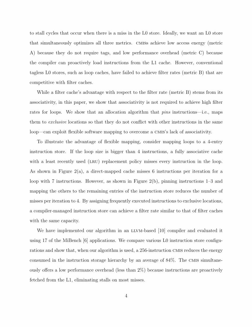
To illustrate the advantage of flexible mapping, consider mapping loops to a 4-entry
instruction store. If the loop size is bigger than 4 instructions, a fully associative cache
with a least recently used (lru) replacement policy misses every instruction in the loop.
As shown in Figure 2(a), a direct-mapped cache misses 6 instructions per iteration for a
loop with 7 instructions. However, as shown in Figure 2(b), pinning instructions 1–3 and
mapping the others to the remaining entries of the instruction store reduces the number of
misses per iteration to 4. By assigning frequently executed instructions to exclusive locations,
a compiler-managed instruction store can achieve a filter rate similar to that of filter caches
with the same capacity.
We have implemented our algorithm in an llvm-based [10] compiler and evaluated it
using 17 of the MiBench [6] applications. We compare various L0 instruction store configu-
rations and show that, when our algorithm is used, a 256-instruction cmis reduces the energy
consumed in the instruction storage hierarchy by an average of 84%. The cmis simultane-
ously offers a low performance overhead (less than 2%) because instructions are proactively
fetched from the L1, eliminating stalls on most misses.
4

1234567
A loop with7 instructions A 4-entry
Instruction Store
(a) A mapping of direct-mapped cache.
1234567
A loop with7 instructions A 4-entry
Instruction Store
(b) An alternativemapping.
Figure 2: Two mappings of a 7-instruction loop to a 4-entry instruction store. The instruc-tion store misses shaded instructions for each iteration. A direct-mapped cache misses 6instructions for each iteration, while an alternative mapping misses 4 instructions.
The remainder of this paper is organized as follows. Section 2 describes our target
architecture. Section 3 describes the concept of pinning on which our algorithm is based.
Section 4 describes our algorithm. Section 5 presents the results of our evaluation. Section 6
reviews related work, and Section 7 concludes.
2 Architecture
A compiler-managed instruction store uses a dual-port (1 read and 1 write) ram so that
the processor can continue to execute instructions from the cmis while instructions are
being loaded. The read port is addressed by an instruction store pointer (isp) to select the
current instruction. The write port is controlled by a transfer engine that transfers blocks
of instructions from the instruction cache to the cmis.
Two instructions “fetch a b n” and “jfetch a b n” transfer n instructions from the
instruction cache at address b to the cmis at address a. Address a is a short index into
the cmis, while address b is a global virtual address that is stored in the immediate field of
an instruction or in a register. For example, “fetch i0 1000 58” transfers 58 instructions
5

1000:
1054: fetch i58 1058 6...1057: 1058:
1063: jfetch i58 1064 6
999: fetch i0 1000 58
1075: fetch i0 1076 81076:
i58
i064-entry CMIS
1064:
1069: jfetch i58 1070 61070:
1074: jump.lt i0
76 instructions
18 instructions
Figure 3: A code snippet of a loop and its mapping to a 64-entry cmis
from the instruction cache, starting at address 1000, to the cmis locations 0–57. In addition
to fetching instructions, jfetch jumps to the target cmis index. All branch targets are
specified by short cmis indices. To synchronize execution with instruction transfer, the
processor stalls when the entry specified by the isp waits for a pending instruction transfer.
Figure 3 shows how a loop is mapped to a 64-entry cmis. The initial instruction loads 58
instructions, starting from address 1000, into cmis locations 0 to 57. These 58 instructions
remain pinned in these locations for the duration of the loop. Control enters the loop as
the isp wraps from 63 to 0. Before the end of this block is reached, the instruction at cmis
location 54 prefetches the next six instructions into the remaining locations, 58 to 63. By the
time execution reaches location 58, these instructions will have been loaded and are ready
to execute. The last 18 instructions of the 76-instruction loop all share locations 58 to 63
with a jfetch instruction transferring each block just before it is needed. Instruction 1074
conditionally jumps back to the start of the loop in location 0. If this jump is not taken,
control falls through to instruction 1075, which loads a different block of code into location
0 and then falls through as the isp wraps to 0.
6

0
50
100
150
200
250
300
50 100 150 200 250# o
f m
isse
s p
er
itera
tio
n
L
FADMCMISLC
Figure 4: The number of misses per iteration for straight-line loops where C = 64
3 Approach
This section demonstrates that, for loops, pinning maximizes the filter rate of L0 stores
without associativity.
For a cache of size C and straight-line loop of length L, the number of misses per iteration
(y) for a fully associative filter cache (fa), a direct-mapped filter cache (dm), and a loop
cache (lc) are as in the following equations. Here, we ignore compulsory misses and assume
that a loop cache can partially capture a loop [12].
yfa =
0 if L ≤ C,
L if L > C
(1)
ydm =
0 if L ≤ C,
2(L− C) if C < L ≤ 2C,
L if L > 2C
(2)
7

1
24
3
L
L-1
fetch 1
fetch L
fetch 1
fetch 2
fetch 4
fetch 3
fetch L-1 fetch L-1
(a)
1
24
3
L
L-1
fetch {L-1,L,1,2}
fetch 4
fetch 3
(b)
1
2
4
3
L
L-1
fetch {L-1,L,1,2}
fetch {L-1,L,1,2,4}
fetch 3
(c)
Figure 5: Reducing L1 cache accesses of loops with branches with pinning(a) An initial fetch schedule(b) A schedule after pinning 1, 2, L-1, and L. Fetches of 1, 2, L-1, and L inside the loop areeliminated by adding fetches of them at the incoming edge of the loop.(c) A schedule after pinning 1, 2, L-1, and L when the inner loop 3 is big so that it conflictswith pinned instructions.
ylc =
0 if L ≤ C,
L− C if L > C
(3)
Just as a loop cache keeps C instructions and misses the other L− C instructions, if we
exclusively assign (pin) x instructions, a cmis misses L− x instructions. When we account
for the overhead from adding fetch instructions, we get
ycmis = L− x +
⌈L− x
C − 2− x
⌉(4)
Figure 4 summarizes our analysis. In the graph, cmiss use the optimal x for each L
value. For straight-line loops, a loop cache suffers the fewest misses because the captured
loop segment does not conflict with the remaining segment (however, a loop cache does not
work for loops with branches). After loop caches, cmiss have the fewest misses. We can see
that, for straight-line loops, associativity does not help and pinning minimizes the miss rate
of cmiss.
8

However, associativity can be beneficial in loops with branches. If an L0 store has
associativity as filter caches do, we can assign instructions with weak temporal relations [3]
to the same location without incurring many conflict misses. Suppose that a loop has
instructions a and b, and that the loop typically executes a during its first half iterations
and b later. In this case, assigning a and b to the same L0 location introduces few conflict
misses. On the other hand, if an L0 store lacks associativity, as cmiss do, the compiler must
conservatively assume that b may have been executed between consecutive executions of a.
Consequently, if we assign a and b to the same location, the compiler must fetch a from
the L1 either immediately before every execution of a, or immediately after every execution
of b. Although many of these fetches will transfer instructions that are already in the L0,
the compiler needs them to make sure that a is present in the L0 before every time it is
executed. Instead of relying on temporal relations, we pin frequently executed instructions
to exclusive locations so that they do not conflict with other instructions in the same loop.
In Appendix A, we formally show that pinning achieves a near-optimal L1 access reduction
for cmiss.
Figure 5 shows examples of pinning a loop with branches. In (a), as an initial schedule
we fetch every instruction just before it is needed. In (b), we pin 1, 2, L-1, and L and
fetch them before entering the loop. By doing this, we can eliminate fetches inside the loop
because there are no conflicts with other instructions for the duration of the loop. In (c),
we pin the same instructions, but the loop has a big inner loop which conflicts with the
pinned instructions. In this case, we can still reduce the number of L1 accesses by fetching
the pinned instructions after executing the inner loop, provided that pinned instructions are
more frequently executed than the inner loop.
9

procedure allocateCMIS(ControlFlowGraph cfg) {T = constructLoopTree(cfg);relayout(cfg, T );initialSchedule(cfg);for each non-leaf node L of T in a post-order {
pin(L, T );schedule(L, T );
}addFetchesAndJumps();allocate(T );emitCode();
}
Figure 6: A high-level description of the algorithm
4 Algorithm
Based on the approach just described, this section details how our algorithm finds the set of
instructions to be pinned to minimize the number of L1 accesses. We process each control
flow graph by traversing the call graph in a reverse post order. For each control flow graph, we
construct an initial schedule, optimize the initial schedule by pinning loops starting from the
inner-most ones, and finally generate assembly code. Figure 6 shows a high-level description
of our algorithm whose sub-steps are described in the following sections.
Relayout To determine which instructions should be pinned, we estimate the relative
frequency at which the basic blocks in a loop are executed. The execution frequency can be
estimated using either a static analysis or profiling information. Both methods are compared
in the evaluation section. In the static analysis, we build a sub-region graph, a directed acyclic
graph in which the back-edge is removed and inner loops are contracted as nodes, as shown
in Figure 7(a). In the sub-region graph, starting from the loop entry, we propagate the
execution probability assuming that each branch direction is independently taken with 50%
probability. The basic blocks in Figure 7 are numbered to reflect the frequency at which
10

5, 6, 74
3
1
2
0.5
0.5
0.250.25
0.25
0.25
(a)
5
6
7
4 call
3
1
Entry
2
Exit
fetch 2
fetch 1
fetch 3
fetch 4
fetch 2
fetch 2
fetch 5
fetch 5
fetch 1
fetch 6
fetch 7
size 66
size 2
size 2
(b)
51
6
7
4 call
3
1
Entry
2
Exit
fetch 2
fetch 1
fetch 3
fetch 4
fetch 2
fetch 2
fetch 51
fetch 1
fetch {6, 7}
size 58
52aa
fetch 52
53aa
size 4
size 4
fetch 53
size 2
size 2
(c)
51aa
6
7
4 call
3
1
Entry
2
Exit
fetch {1,2}
fetch 3
fetch 4
fetch {1,2}
fetch 51
fetch {6,7}
size 58
52aa
fetch 52
53aa
size 4
size 4
fetch 53
fetch {1,2}
size 2
size 2
(d)
Figure 7: An example of allocating loops to a 64-entry cmis.In (b)-(d), pinned instructions are shaded. Basic blocks are numbered according to the or-dering after relayout; we generate the code following this ordering in our algorithm’s outputassembly code. Block 4 has a function call whose callee uses the entire cmis.(a) The sub-region graph of the loop {1, 2, 3, 4, 5, 6, 7}, in which each edge is annotatedwith the execution probability per iteration computed by a simple static analysis(b) A schedule after pinning loop {6}. Since this loop fits within the cmis, the entire loopis pinned.(c) A schedule after pinning loop {5, 6, 7}. An optimum size of pinning is 58, so 58 instruc-tions of block 5 are pinned and extracted as a separate block 51.(d) A schedule after pinning loop {1, 2, 3, 4, 5, 6, 7}. This loop has an inner loop biggerthan the cmis size and a function call. According to the probabilities annotated in (b), theprobability of executing the inner loop or the function call per iteration is 0.5. Since 1 and2 are the only ones with execution probability higher than 0.5, we pin 1 and 2.
11

blocks are executed, with the more frequently executed blocks assigned smaller numbers.
The basic blocks are laid out so that the most frequently executed blocks are contiguous in
memory and can be fetched as a single group.
Initial Schedule We construct an initial fetch schedule in which each instruction is
fetched just before it is executed. Though correct, this schedule is inefficient and we optimize
it as follows.
Instruction Pinning For each loop L, we select instructions to pin, which we call
fetch block P . We find P with the lowest cost (fetching the smallest number of unpinned
instructions per iteration) subject to the following three constraints:
1. |P | ≤ C, where C is the cmis size.
2. P is a contiguous block of instructions that includes the loop entry.
3. Let S = {inner loop M in L such that |M ∪ P | > C}. ∀ instruction x ∈ P , Pr(x) >
Pr(S), where Pr(x) is the probability of executing x per iteration.
The first constraint is trivial. The second constraint ensures that the pinned instructions
are contiguous in memory. The third constraint minimizes the conflicts between pinned
instructions and unpinned inner loops. Since an inner loop M and pinned instructions P
cannot both fit within the cmis if |M ∪ P | > C, we need to fetch the conflicting part of P
after executing M . This constraint ensures that instructions in P are executed at least once
after they are fetched into the cmis.
For a function call, if the call does not belong to a cycle in the call graph, we propagate
pinning information from the callee. If the call does belong to a cycle, we treat the function
call as if it is an inner loop with size bigger than C. Figure 7(d) shows an example of applying
the third constraint: 3 is not pinned because the probability of executing it does not exceed
the probability of executing the function call in 4 or the inner loop {5, 6, 7}.
12

For each pinned fetch block candidate, P , we form unpinned fetch blocks from remaining
instructions. First, each unpinned basic block bigger than C − |P | is divided into multiple
blocks that are smaller than C − |P |. For example, in Figure 7(c), we divide 5’s unpinned
instructions into 52 and 53. Then, unpinned fetch blocks forming a chain are merged if their
collective size does not exceed C − |P |. For example, in Figure 7(c), we merge 6 and 7.
For each candidate P , we compute the following cost function which sums up the ex-
ecution probability of unpinned instructions. There are at most C candidates because of
constraints 1 and 2. Among them, we select a P that minimizes the cost function.
cost(P ) =∑
∀unpinned fetch block U of P
Pr(U) · |U | (5)
Fetch Scheduling We add fetches of pinned fetch blocks at incoming edges of the loops
(e.g., fetch {1, 2} is added at the edge from the entry to 1 in Figure 7(d)). If there is an
inner-loop or a function call that conflicts with the pinned instructions, we also add fetches
to load the conflicting pinned instructions at the outgoing edges (e.g., fetch {1, 2} at the
edge from 4 to 2 and the edge from 7 to 2 in Figure 7(d)). Then we eliminate redundant
fetches of pinned instructions inside the loop (e.g., at the edge from 1 to 2 in Figure 7(d)).
Post-processing We modify the code by adding fetches and jumps, allocate instructions
to cmis locations, and finally generate the modified assembly code.
To avoid an unnecessary fetch at a basic block with outgoing edges with different fetch
sets (e.g. basic block 3 in Figure 7(d)), we modify jumps as shown in Figure 8. For function
calls, we always jump to i0 and returns to i0 as shown in Figure 9. We generate an entry
code for the callee and a resuming code for the caller starting from i0 (see @callee entry
and @caller resume). The caller pushes the address of the resuming code, and the callee
returns by a jfetch to the pushed address.
We allocate instructions to CMIS locations as we traverse the loop tree in a post-order.
13

@bb_i: ...
...
jump.lt @taken
@nontaken: ...
(a)
@bb_i: ...
...
jump.lt @bb_i_t
jfetch i17 @nontaken 15
@bb_i_t: jfetch i32 @taken 7
@nontaken: ...
(b)
Figure 8: Modifying a jump to avoid an unnecessary fetch when outgoing edges of bb i havedifferent fetch sets. (a) Before and (b) after the modification.
push @caller_resume
jfetch i0 @callee_entry 1 // function call
@caller_resume: jfetch i32 @caller_next_fblock 4
// always allocated to i0
...
@callee_entry: fetch i1 @callee_first_fblock 5
// always allocated to i0
...
pop r0
jfetch i0 r0 1 // return
Figure 9: A function call code snippet
14

Table 2: Experimental Setup
BaselineNo L0 instruction store
4-way 16kb L1 I-cache with 8-entry cache lineslc Loop cache with flexible loop size scheme [12]
faFully associative cache with lru replacement policy
and 8-entry (32-byte) cache linesdm Direct-mapped cache with 8-entry cache linescmis Baseline compiler-managed instruction storecmis p cmis with profilingopt fa with optimal replacement policy
When we visit a loop, we first sequentially allocate pinned instructions starting from the
current base address, then we allocate unpinned fetch blocks to the remaining CMIS entries
as shown in the pseudo code Figure 10.
5 Evaluation
This section describes the experimental setup for our algorithm evaluation and analyzes the
results.
5.1 Experimental Setup
For our evaluation, we use ELM [1], a multi-core architecture with an explicitly forwarded
inorder dual-issue pipeline with 4 stages, software-managed memories, and a mesh on-chip
interconnection network. To make our evaluation less sensitive from ELM-specific features,
we modify the architecture model to a single-core one with a run-time forwarded single-issue
pipeline and an L1 instruction cache, and change the compiler and the simulator accordingly.
Our algorithm is implemented in elmcc, a compiler back-end for ELM that reads fully-
optimized llvm intermediate representation [10].
15

procedure allocate(LoopTree T ) {allocateRecursive(T.root, 0);
}
procedure allocateRecursive(Loop L, int base) {G = sub-region graph of L;V = nodes of G sorted by the ordering
constructed from relayout in Figure 6;cmisIndex = base;for each pinned v in V {
if v is a loopcmisIndex = allocateRecursive(v, cmisIndex);
else {allocate v at cmisIndex % C; // C is the CMIS sizecmisIndex += |v|;
}}unpinnedBase = cmisIndex;for each unpinned v in V {
if cmisIndex + |v| ≥ base + C and L is not the rootcmisIndex = unpinnedBase;
if v is a loopcmisIndex = allocateRecursive(v, cmisIndex);
else {allocate v at cmisIndex % C;cmisIndex += |v|;
}}return cmisIndex;
}
Figure 10: A pseudo code of allocation
16

We use all the integer and fixed-point applications of MiBench [6]. We also use fft in
MiBench after converting its floating point operations to fixed-point ones. We exclude the
other applications because our processor does not support floating point operations.
Table 2 summarizes the configurations used in the evaluation. We compare cmiss with
32–512 instructions to fully associative (fa) filter caches [9], direct-mapped (dm) filter caches,
and loop caches (lc) [11,12] with the same size. To provide a lower bound for the number of
L1 cache accesses, we include fully associative caches with an optimal replacement policy [2]
(opt). For fa and dm, we use 8-instruction (32-byte) cache lines, which achieve the best
energy-delay product [4], under the assumption that the instruction cache consumes 27% of
the total energy as in the StrongARM processor [13]. To control for improvements due to
code relayout, we apply the same relayout algorithm for dm when it is beneficial. The basic
cmis configuration uses a simple static method for computing execution frequency, while the
cmis p configuration uses profiling. We use a 16kb L1 instruction cache with 8-instruction
cache lines and 4-way set associativity. The L1 instruction cache with no L0 instruction
store is the baseline of our comparison.
Table 3 lists the energy of each operation estimated from detailed circuit models of caches
and memories realized in a commercial 45 nm low-leakage cmos process. The models are val-
idated against hspice simulations, with device and interconnect capacitances extracted after
layout. Leakage current contributes a negligibly small component of the energy consumption
because low-leakage devices are used. dms use srams to store tags and instructions; the tag
array and data array are accessed in parallel, and the tag check is performed after both
arrays are accessed. fas use cams to store the tags and srams to store the instructions. fas
are designed so that the sram is only read when there is a hit in the tag cam; consequently,
a miss consumes less energy, as only the tag array is accessed. When transferring instruc-
tions from the L1 cache, the L1 tag is checked once and the instructions are transferred over
multiple cycles.
17

Table 3: Energy per Operation in pJ. “Refill” is per cache line size energy.
Hit [pJ] Miss [pJ] Refill [pJ]32-entry fa 0.28 0.09 3.7664-entry fa 0.50 0.17 6.04128-entry fa 0.92 0.33 10.60256-entry fa 1.74 0.62 19.70512-entry fa 3.37 1.18 37.9332-entry dm 0.23 0.23 3.7364-entry dm 0.39 0.39 5.99128-entry dm 0.72 0.72 10.50256-entry dm 1.35 1.35 19.55512-entry dm 2.64 2.64 37.6432-entry cmis 0.11 — 0.3364-entry cmis 0.18 — 0.61128-entry cmis 0.33 — 1.16256-entry cmis 0.63 — 2.26512-entry cmis 1.22 — 4.4716kb L1 20.35 2.68 37.01
5.2 L1 Cache Accesses
Figure 11(a) compares the number of L1 cache accesses for each configuration. The number
of L1 cache accesses is normalized to that of the baseline (no L0 store) and accounts for the
additional fetch instructions in the cmis configuration. As expected, the number of accesses
declines as the capacity increases. At smaller capacities, cmiss perform better than filter
and loop caches. At larger capacities, filter caches perform better because they capture
instruction reuse that spans multiple function invocations. Larger loop caches offer little
improvement because there are few straight-line loops with more than 32 instructions, which
is consistent with [5].
Figure 11(b) shows the number of L1 cache accesses for each benchmark for the 256-
instruction configurations. The cmiss perform better than the dm filter cache on applica-
tions dominated by loops that exhibit regular control flow (mad, blowfish, rijndael, and
18

0.0
0.1
0.2
0.3
0.4
0.5
0.6
32 64 128 256 512
No
rmalize
d L
1 A
ccess
Co
un
t
Capacity [instructions]
LC
FA
DM
CMIS
CMIS_P
OPT
(a) The number of L1 accessesnormalized to the baseline
0.00.10.20.30.40.50.60.70.80.91.0
No
rmalize
d L
1 A
ccess
Co
un
t
LC FA DM CMIS CMIS_P OPT
(b) The number of L1 accesses. Each shows the number of L1accesses normalized to the baseline, in which no L1 access is filtered.
0.0
0.1
0.2
0.3
0.4
0.5
0.6
32 64 128 256 512No
rmalize
d I
nst
ruct
ion
Fetc
h
En
erg
y
Capacity [instructions]
LC FA DM CMIS CMIS_P
(c) The energy consumed in theinstruction storage hierarchynormalized to the baseline
0.00.10.20.30.40.50.60.70.80.91.0
No
rmalize
d I
nst
ruct
ion
Fetc
h
En
erg
y
LC FA DM CMIS CMIS_P
(d) Normalized energy of L0 instruction stores with 256 entries
0
1
2
3
4
5
6
7
8
32 64 128 256 512
Execu
tio
n T
ime I
ncr
ease
[%
]
Capacity [instructions]
DM
CMIS
CMIS_P
(e) Execution time increase fromthe baseline
0.0
0.1
0.2
0.3
0.4
0.5
0.6
0.05 0.10 0.15 0.20 0.25No
rmalize
d I
nst
ruct
ion
Fetc
h
En
erg
y
Normalized L0 Hit Energy
LC FA DM CMIS_P
CACTI 5.0 withdefault option
CACTI 5.0 withdynamic energy optimization option,
Ravindran et. alOurs
(f) Sensitivity of energy saving on the L0 to L1 access energy ratio.Normalized L0 hit energy denotes the hit energy of the
256-instruction dm normalized to that of L1.
Figure 11: L1 accesses, energy consumption, and execution time results. The averages are obtained bycomputing arithmetic means over per-instruction-value of each benchmark and then normalizing the meansto the baseline processor configuration.
19

gsmencode). The dm performs better on applications with less predictable, irregular control
flow (cjpeg, patricia, ispell, and pgp), where its associativity allows it to capture reuse
that the compiler is not able to exploit due to its conservativeness; 34% of the L1 cache ac-
cesses by the 256-instruction cmis p in these applications are unnecessary ones which fetch
instructions that are already in the cmis.
5.3 Energy Consumption
Figure 11(c) shows the energy consumed in the L0 and L1 stores for each configuration.
Figure 11(d) shows the energy consumed in each of the benchmarks. The best cmis config-
uration (the 256-instruction cmis p) achieves an 84% reduction; the best fa and dm filter
cache configurations (the same size fa and dm) achieve 73% and 78% reductions, respec-
tively. While the 256-instruction cmis p reduces the energy consumed in the L0 by 45%
compared to the same size dm, its overall energy reduction from the dm is 26%. This is
because the cmis p and dm consume about the same L1 energy, which constitutes 43% of
the total energy consumed by the L0 and L1 stores in the dm configuration.
To provide context, an 84% reduction in the energy consumed by the instruction storage
hierarchy would result in a 23% reduction in the total dynamic energy consumed in processors
such as the StrongARM [13], in which 27% of the total dynamic energy is consumed by the
instruction cache.
The fetch instructions increase the code size by, on average, 6%. This increases the energy
consumed by the next level memory (an off-chip main memory or an L2 cache) by fetching
more instructions from it. However, even if we pessimistically assume that an access to the
next level consumes 100× more energy than that to the L1, cmiss’ energy saving is still
bigger than other L0 stores: the 256-instruction cmis saves 75% of the energy consumed by
the instruction hierarchy (including the next level memory energy), while the 256-instruction
20

dm saves 72%.
To illustrate the sensitivity of these results to the memory energy models, Figure 11(f)
shows how the energy consumption changes as the ratio of the 256-instruction dm hit energy
to that of L1 varies. Since the cache architecture assumed by cacti [16] mainly targets
caches that are bigger than or equal to typical L1 cache sizes, it tends to overestimate
energy consumption in small L0 stores, as shown at the points denoted as “cacti” in Fig-
ure 11(f). Consequently, the cacti model over-emphasizes a weakness of filter caches that
they consume more L0 access energy than other L0 stores.
5.4 Performance
Figure 11(e) compares the performance overhead of L0 stores. We assume a penalty of 1
cycle for each filter cache miss as in [8,9] and a load-use penalty of 1 cycle for cmiss. For an
indirect fetch whose target memory address is stored in a register, we assume a penalty of
2 cycles. The processor allows one outstanding fetch and stalls when a second is attempted
before the first completes. To focus on the aspect of instruction fetch, we ignore L1 cache miss
and branch miss prediction penalty in Figure 11(e). Within this setup, the 256-instruction
cmis incurs a 1.8% performance overhead1.
Gordon-Ross et al. [5] report more than 20% performance overhead for filter caches, while
Hines et al. [8] report about 4% overhead. We find that the 256-instruction dm filter cache
incurs a 1.7% performance overhead, which is more closely aligned with Hines et al. [8]. This
is because, whereas Gordon-Ross et al. [5] assume a penalty of 4 cycles for each filter cache
miss, we assume a penalty of 1 cycle as in Hines et al. and Kin et al. [8, 9]. The 1 cycle
penalty can be achieved by critical word first technique [7]. We also optimize the cache line
1 This is an upper bound of cmiss’ performance overhead because its baseline is an ideal case withoutL1 cache and branch miss prediction penalty; e.g., if we assume an L1 cache miss penalty of 32 cycles, an128-instruction bimodal branch predictor, and a branch miss penalty of 2 cycles, the 256-instruction cmis’sperformance overhead reduces to 1.1%.
21

size for the best energy-delay product [4]. By increasing the cache line size, we capture more
spatial locality and miss fewer instructions, resulting in a lower performance overhead [7].
However, at the same time, this leads to the transfer of more unnecessary instructions from
the L1 cache. We find that 8-instruction cache lines balance this trade-off and achieve the
best energy-delay product. For example, by increasing the cache line size from 2 to 8, the
performance overhead of the 256-instruction dm filter cache decreases from 5.8% to 1.7%,
while the reduction of normalized L0 and L1 store energy changes minimally (from 78.4%
to 78.3%).
6 Related Work
Filter caches [9] have been criticized for their performance overhead. However, in this paper,
we show that a filter cache can achieve a low performance overhead. Although they consume
more energy than cmiss on average, filter caches can be useful for applications with irregular
control flows.
Loop caches [11, 12] are L0 stores that serve well for applications in which straight-line
loops dominate the performance. However, Gordon-Ross et al. [5] and our results demon-
strate that the original loop cache design [11,12] is inflexible in dealing with diverse embedded
applications. Gordon-Ross et al. [5] address this by pre-loading performance critical loops
with arbitrary shapes. However, as Ravindran et al. [15] show, the pre-loaded loop cache
design cannot overlay loops in different program phases, and thus cannot use the loop cache
capacity efficiently.
Ravindran et al. [15] have an approach similar to ours in that the compiler modifies code
for an L0 store to dynamically load instructions. However, their algorithm unnecessarily
uses data structures such as a temporal relation graph [3] without considering that their
loop caches lack associativity, as cmiss do. If a store has associativity, assigning instructions
22

with weak temporal relations [3] to the same location introduces few conflict misses. However,
if a store lacks associativity, as their loop caches do, the same assignment is not useful for
maximizing the filter rate due to the compiler’s conservativeness, as described in Section 3.
In addition, whereas profiling information is required for the algorithm in Ravindran et
al. [15], profiling is dispensable in ours as demonstrated in Figure 11(c), which simplifies the
compilation procedure.
Hines et al. [8] propose an L0 instruction store design called tagless hit instruction cache
(th-ic). th-ics determine if an instruction fetch will be a hit by looking up its metadata,
which consumes less energy than checking tags. However, the authors do not report how
much energy is spent on maintaining the metadata and the control logic. Even if we com-
pletely ignore this energy and use the best policy reported in [8] (tl policy), our evaluation
shows that their best energy reduction is 83%, which is smaller than that of cmiss.
A significant amount of research has been done on scratch-pad memories [14]. Although
both scratch-pad memories and cmiss are tagless and managed by the compiler, cmiss
are smaller than typical scratch-pad memories and mainly target locality that comes from
loops. In addition, a cmis is another level of the instruction storage hierarchy that every
instruction must go through to be executed, whereas a scratch-pad memory is often an
alternative location to store instructions or data.
7 Conclusion
This paper presents an allocation algorithm based on pinning that achieves a near-optimal
fetch count reduction of cmiss for loops. In spite of the lack of associativity, pinning allows
cmiss to achieve L1 cache access reductions similar to those of filter caches, with low L0
access energy and performance overhead. This is in contrast to loop caches [5, 11, 15] that
achieve low L0 access energy and performance overhead at the expense of more L1 cache
23

accesses than filter caches.
This paper also re-evaluates filter caches. Although filter caches are not as energy efficient
as cmiss, accurate memory energy modeling and line size tuning can make filter caches’
energy consumption and performance overhead smaller than what previous work [5, 9] has
reported.
References
[1] J. Balfour, W. J. Dally, D. Black-Schaffer, V. Parikh, and J. Park. An Energy-EfficientProcessor Architecture for Embedded Systems. Computer Architecture Letters, 7(1), 2008.
[2] L. A. Belady. A Study of Replacement Algorithms for Virtual-storage Computer. IBM SystemsJournal, 5(2):78–101, 1966.
[3] N. Gloy and M. D. Smith. Procedure Placement using Temporal-ordering Information. ACMTransactions on Programming Languages and Systems (TOPLAS), 21(5):977–1027, 1999.
[4] R. Gonzalez and M. Horowitz. Energy Dissipation in General Purpose Microprocesors. IEEEJournal of Solid-State Circuits, 31(9):1277–1284, 1996.
[5] A. Gordon-Ross, S. Cotterell, and F. Vahid. Tiny Instruction Caches for Low Power EmbeddedSystems. ACM Transactions on Embedded Computing Systems (TECS), 2(4):449–481, 2003.
[6] M. R. Guthaus, J. S. Ringenberg, D. Ernst, T. M. Austin, T. Mudge, and R. B. Brown.MiBench: A Free, Commercially Representative Embedded Benchmark Suite. In IEEE 4thAnnual Workshop on Workload Characterization, pages 83–94, 2001.
[7] J. L. Hennessy and D. A. Patterson. Computer Architecture: A Quantitative Approach. 2003.[8] S. Hines, D. Whalley, and G. Tyson. Guaranteeing Hits to Improve the Efficiency of a Small
Instruction Cache. In International Symposium on Microarchitecture (MICRO), pages 433–444, 2007.
[9] J. Kin, M. Gupta, and W. H. Mangione-Smith. The Filter Cache: An Energy Efficient MemoryStructure. In International Symposium on Microarchitecture (MICRO), pages 184–193, 1997.
[10] C. Lattner and V. Adve. LLVM: A Compilation Framework for Lifelong Program Aanalysis &Transformation. In International Symposiumon Code Generation and Optimization (CGO),pages 75–86, 2004.
[11] L. H. Lee, B. Moyer, and J. Arends. Instruction Fetch Energy Reduction Using Loop Cachesfor Embedded Applications with Small Tight Loops. In International Symposium on LowPower Electronics and Design (ISLPED), pages 267–269, 1999.
[12] L. H. Lee, B. Moyer, and J. Arends. Low-Cost Embedded Program Loop Caching - Revisited.Technical Report CSE-TR-411-99, University of Michigan, 1999.
[13] J. Montanaro, R. T. Witek, K. Anne, A. J. Black, E. M. Cooper, D. W. Dobberpuhl, P. M.Donahue, J. Eno, G. W. Hoeppner, D. Kruckemyer, T. H. Lee, P. C. M. Lin, L. Madden,D. Murray, M. H. Pearce, S. Santhanam, K. J. Snyder, R. Stephany, and S. C. Thierauf. A160-MHz, 32-b, 0.5-W CMOS RISC Microprocessor. IEEE Journal of Solid-State Circuits,31(11):1703–1714, 1996.
24

[14] P. R. Panda, N. D. Dutt, and A. Nicolau. Efficient Utilization of Scratch-Pad Memory inEmbedded Processor Applications. In European Design and Test Conference, pages 7–11,1997.
[15] R. A. Ravindran, P. D. Nagarkar, G. S. Dasika, E. D. Marsman, R. M. Senger, S. A. Mahlke,and R. B. Brown. Compiler Managed Dynamic Instruction Placement in a Low-Power CodeCache. In International Symposium on Code Generation and Optimization (CGO), pages179–190, 2005.
[16] S. J. Wilton and N. P. Jouppi. CACTI: An Enhanced Cache Access and Cycle Time Model.IEEE Journal of Solid-State Circuits, 31(5):677–688, 1996.
A Appendix
Let G be the subgraph of the control flow graph induced by a loop without any inner loops,
L. Let the target and source of L’s back-edge be the entry and the exit of G, respectively.
A set S dominates a node x, denoted by S dom x, if every path from the entry to x must
go through at least one element in S. A set S post-dominates a set T , denoted by S pdom
T , if every path from an element in T to the exit must go through at least one element in
S. Let F (x) be the set of program locations in L where a “fetch x” resides. Let Xi be the
set of instructions that are allocated to the ith cmis location.
We can easily show the following Lemma by proving its contrapositive using the definition
of dom and pdom.
Lemma A.1 For a correct fetch schedule,∀x ∈ Xi,
(F (x) dom x) ∨
((F (x) pdom Xi − {x}) ∧
(x resides at the ith cmis location at the incoming edge of L)).
Let p(x) be the execution count of x and p(S) =∑
x∈S p(x). Let the baseline be a schedule
such that ∀x ∈ L, p(F (x)) = p(x); e.g., fetch x right before executing x. If x satisfies the
first clause of Lemma 1 (i.e. F (x) dom x), then p(F (x)) ≥ p(x). Therefore, the only way of
reducing p(F (x)) from the baseline is the second clause, but at most one instruction in Xi can
25

satisfy the second clause because only one can reside at the ith cmis location at L’s incoming
edge. Hence, the implication of Lemma 1 is that, among the instructions allocated to the
same cmis location, at most one can have a smaller fetch count than the baseline. Using
this, we can show that pinning achieves a near-optimal fetch count reduction as follows.
Proposition A.1 Let OPT be the optimal fetch count reduction 2from the baseline. Let C
be the size of a cmis. Allocating C − 1 highest frequency instructions to exclusive locations
and allocating all the others to the remaining location achieves a fetch count reduction no
smaller than C−1C
OPT .
Proof of Proposition A.1. By Lemma 1, we can reduce fetch count of at most C instruc-
tion, one each from X1, X2, ..., XC . Let p(xj) be the jth largest among {p(x) | x ∈ L}.
Then OPT is bounded by∑C
j=1 p(xj): map C highest frequency instructions to locations 1
to C and reduce their fetch counts to 0. Let PIN be the fetch count reduction by allocating
C − 1 highest frequency instructions to exclusive locations.
PIN ≥C−1∑j=1
p(xj) =C∑
j=1
p(xj)− p(xC) ≥ OPT − 1
COPT
�
2 It is optimal under the assumption that modifying the structure of control flow is not allowed. Forexample, we can split a loop by its iteration space and specialize each split loop by optimizing for thelocality in its sub-iteration space.
26