ST11 – Transistor 1 Transistor Lecturer: Smilen Dimitrov Sensors Technology – MED4.
31
1 ST11 – Transistor Transistor Lecturer: Smilen Dimitrov Sensors Technology – MED4
-
Upload
kerry-riley -
Category
Documents
-
view
239 -
download
0
Transcript of ST11 – Transistor 1 Transistor Lecturer: Smilen Dimitrov Sensors Technology – MED4.
1
ST11 – Transistor
Transistor
Lecturer:Smilen Dimitrov
Sensors Technology – MED4
2
ST11 – Transistor
Introduction
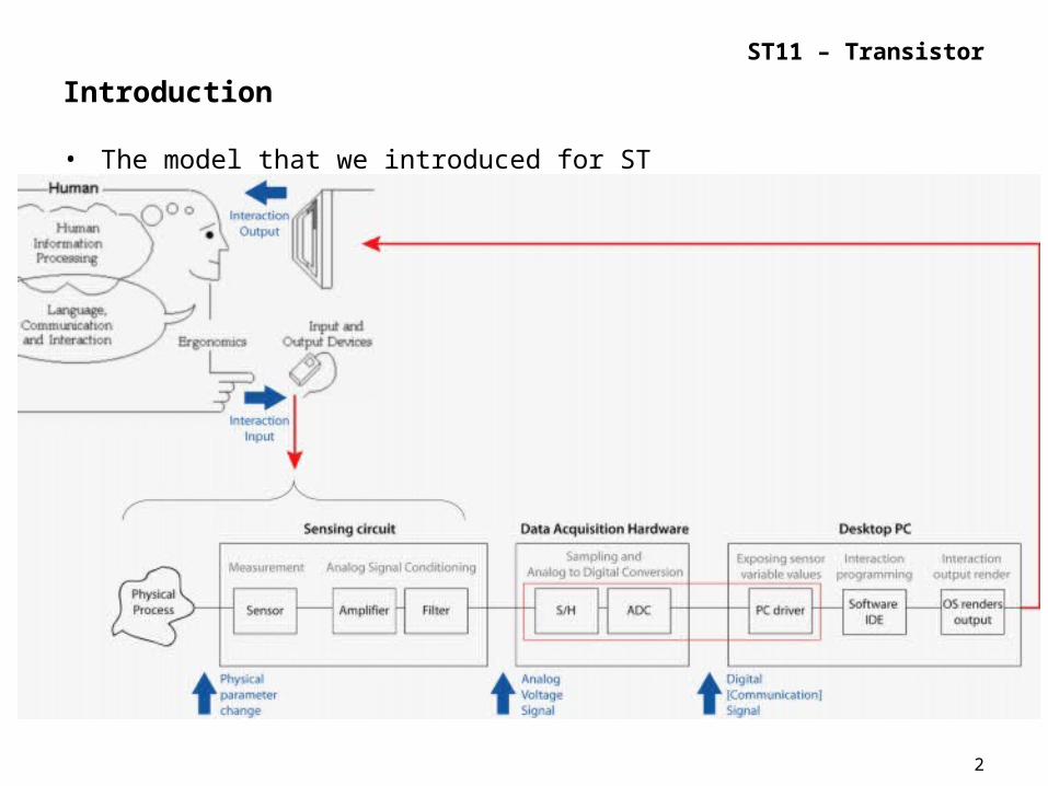
• The model that we introduced for ST
3
ST11 – Transistor
Introduction
• We have discussed
– The units of voltage, current and resistance, from both a microscopic and macroscopic (electric circuits) perspective
– The definition of an elementary electric circuit, Ohm’s law and Kirschoff Laws
– Solving and measurement of voltage divider circuit and more complicated circuits - and applications in sensors
– Resistive based sensors– AC current, capacitors, and capacitive based sensors– Semiconductor structures – diode (and sensor applications)
• This time we discuss the transistor as an electronic element, and as a basis for different types of sensors
4
ST11 – Transistor
Transistor
• Transistor is a semiconductor device as well - however, it has three terminals - so a bit more complex to understand.
– the application of voltage to the input terminal, changes the conductivity between the other two terminals, and hence controls current flow through those terminals.
• Two basic types of transistors, which differ in construction and usage (but not in main purpose)– bipolar junction transistors (BJTs) – field effect transistors (FETs)
• Other categorizations - a particular transistor may be described as: silicon, surface mount, BJT, NPN, low power, high frequency switch.
– Semiconductor material: germanium, silicon, gallium arsenide, silicon carbide
– Type: BJT, JFET, IGFET (MOSFET), IGBT, "other types"
– Polarity: NPN, PNP, N-channel, P-channel
– Maximum power rating: low, medium, high
– Maximum operating frequency: low, medium, high, radio frequency (RF), microwave
– Application: switch, general purpose, audio, high voltage, super-beta, matched pair
– Physical packaging: through hole metal, through hole plastic, surface mount, ball grid array
5
ST11 – Transistor
Bipolar junction transistor (BJT)
• Called bipolar because conduction channel uses both majority and minority carriers for main electric current– first type of transistor to be commercially mass-produced
• The three terminals are named emitter, base and collector.– Two p-n junctions exist inside the BJT: collector-base junction
and base-emitter junction.– described as a current operated device because the
collector current is controlled by the current flowing between base and emitter terminals.
• in a P semiconductor, majority carriers are holes, and minority carriers are free electrons; – in a N semiconductor, majority carriers are free electrons, and
minority carriers are holes
6
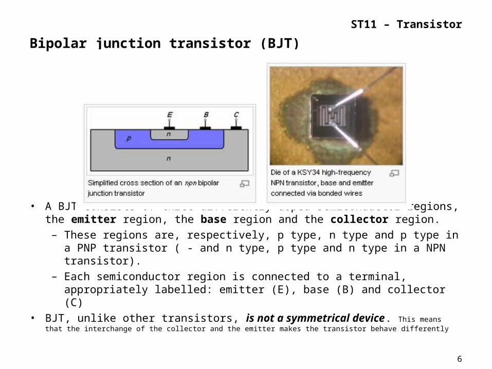
ST11 – Transistor
Bipolar junction transistor (BJT)
• A BJT consists of three differently doped semiconductor regions, the emitter region, the base region and the collector region.– These regions are, respectively, p type, n type and p type in a
PNP transistor ( - and n type, p type and n type in a NPN transistor).
– Each semiconductor region is connected to a terminal, appropriately labelled: emitter (E), base (B) and collector (C)
• BJT, unlike other transistors, is not a symmetrical device. This means that the interchange of the collector and the emitter makes the transistor behave differently

7
ST11 – Transistor
Bipolar junction transistor (BJT)
• Small changes in the voltage applied across the base-emitter terminals, causes the current that flows between the emitter and the collector to change significantly. – This effect can be used to amplify the input current. BJTs can
be thought of as voltage-controlled current sources
• A Bipolar Transistor essentially consists of a pair of PN Junction Diodes that are joined back-to-back. – This forms a sort of a sandwich where
one kind of semiconductor is placed in between two others.
8
ST11 – Transistor
Bipolar junction transistor (BJT)
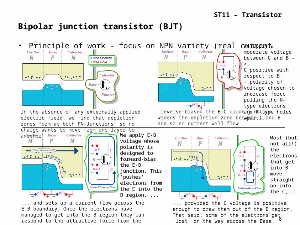
• Principle of work – focus on NPN variety (real current direction)
In the absence of any externally applied electric field, we find that depletion zones form at both PN-Junctions, so no charge wants to move from one layer to another
…reverse-biased the B-C diode junction - widens the depletion zone between C and B and so no current will flow
We apply a moderate voltage between C and B -> C positive with respect to B - polarity of voltage chosen to increase force pulling the N-type electrons and P-type holes apart….
... and sets up a current flow across the E-B boundary. Once the electrons have managed to get into the B region they can respond to the attractive force from the positively-biased C region.
We apply E-B voltage whose polarity is designed to forward-bias the E-B junction. This 'pushes' electrons from the E into the B region, ...
... provided the C voltage is positive enough to draw them out of the B region. That said, some of the electrons get 'lost' on the way across the Base.
Most (but not all!) the electrons that get into B move straight on into the C,...
9
ST11 – Transistor
Bipolar junction transistor (BJT)
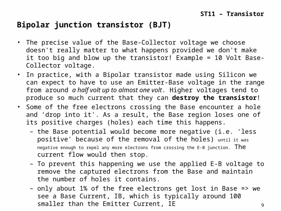
• The precise value of the Base-Collector voltage we choose doesn't really matter to what happens provided we don't make it too big and blow up the transistor! Example = 10 Volt Base-Collector voltage.
• In practice, with a Bipolar transistor made using Silicon we can expect to have to use an Emitter-Base voltage in the range from around a half volt up to almost one volt. Higher voltages tend to produce so much current that they can destroy the transistor!
• Some of the free electrons crossing the Base encounter a hole and 'drop into it'. As a result, the Base region loses one of its positive charges (holes) each time this happens.– the Base potential would become more negative (i.e. 'less
positive' because of the removal of the holes) until it was negative enough
to repel any more electrons from crossing the E-B junction. The current flow would then stop.
– To prevent this happening we use the applied E-B voltage to remove the captured electrons from the Base and maintain the number of holes it contains.
– only about 1% of the free electrons get lost in Base => we see a Base Current, IB, which is typically around 100 smaller than the Emitter Current, IE

10
ST11 – Transistor
Bipolar junction transistor (BJT)
• Transistor - as an current amplifier. When a small current signal is applied to the base terminal, it is amplified in the collector circuit. This current amplification is referred to as hFE or beta (β) and equals Ic/Ib.
• Circuit theory – use technical direction of current
For proper polarization (of NPN), we say:– the base is directly polarised (forward
biased - P base potential is more positive than N emitter
potential)– the collector is inversely polarised
(reverse biased - N collector potential is more
positive than P base potential)
Schematic symbols: The direction of the emitter arrow defines the type of transistor.

11
ST11 – Transistor
Bipolar junction transistor (BJT)
• The transistor is a complex element, and can be used in a variety of ways.
• We will mostly discuss the configuration known as a 'common emitter', (described previously): – base-emitter PN junction is directly polarised, – and collector-base PN junction is inversely polarised.
• For this mode of operation, it is important we remember the following points in analysis (of an NPN transistor) – The base-emitter junction behaves like a diode - that is, it has
a turn-on voltage (as in a diode, approx 0.7V)– When the base-emitter junction is turned on, and base current IB
flows, the collector current IC is related to IB, and amplified by a factor of hFE or beta (β) - that is, IC = hFE* IB.
– hFE is as parameter which is usually 20 or 30, and in high gain transistor this factor can be all the way up to 100 or 200
12
ST11 – Transistor
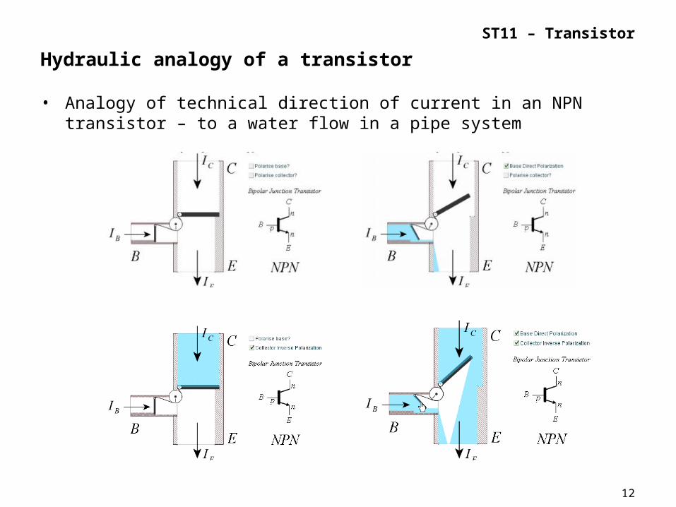
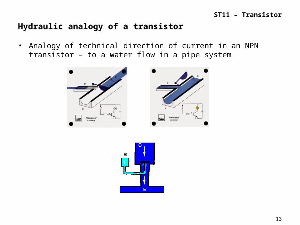
Hydraulic analogy of a transistor
• Analogy of technical direction of current in an NPN transistor – to a water flow in a pipe system
13
ST11 – Transistor
Hydraulic analogy of a transistor
• Analogy of technical direction of current in an NPN transistor – to a water flow in a pipe system
14
ST11 – Transistor
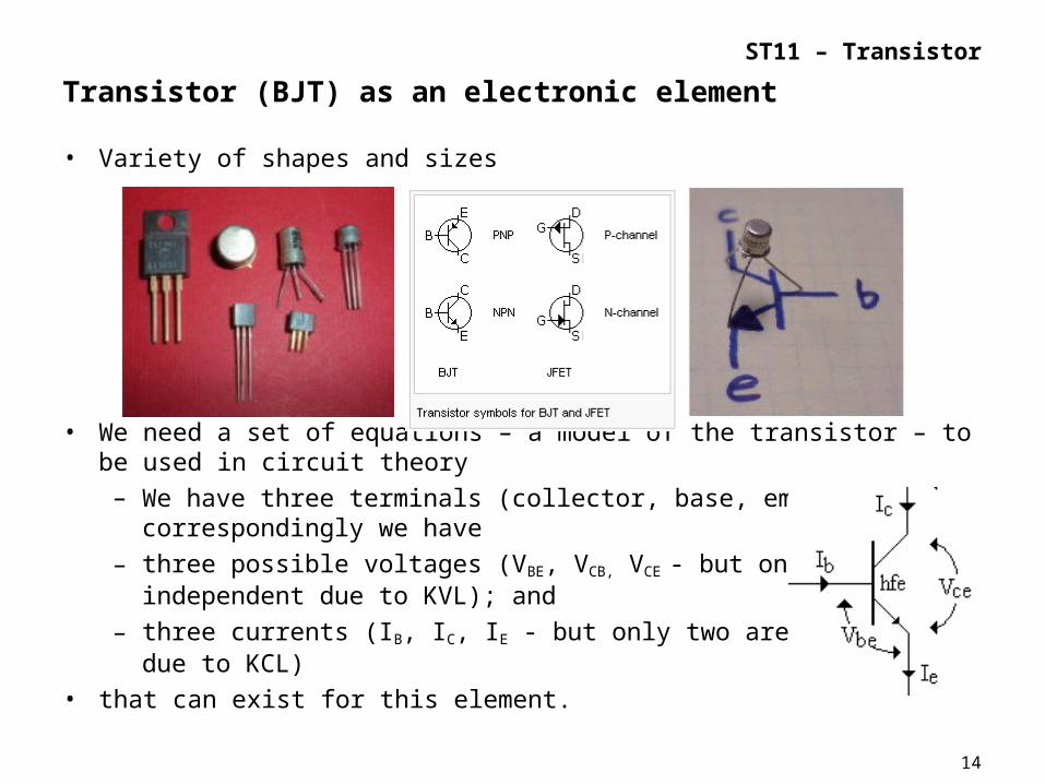
Transistor (BJT) as an electronic element
• Variety of shapes and sizes
• We need a set of equations – a model of the transistor – to be used in circuit theory – We have three terminals (collector, base, emitter), and
correspondingly we have – three possible voltages (VBE, VCB, VCE - but only two are
independent due to KVL); and – three currents (IB, IC, IE - but only two are independent
due to KCL) • that can exist for this element.
15
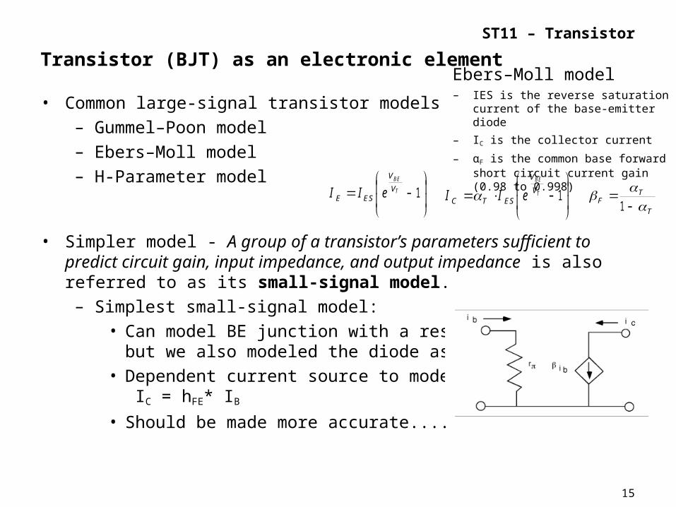
ST11 – Transistor
Ebers–Moll model– IES is the reverse saturation
current of the base-emitter diode
– IC is the collector current
– αF is the common base forward short circuit current gain (0.98 to 0.998)
Transistor (BJT) as an electronic element
• Common large-signal transistor models – Gummel–Poon model – Ebers–Moll model – H-Parameter model
• Simpler model - A group of a transistor’s parameters sufficient to predict circuit gain, input impedance, and output impedance is also referred to as its small-signal model. – Simplest small-signal model:
• Can model BE junction with a resistor,but we also modeled the diode as a switch
• Dependent current source to model IC = hFE* IB
• Should be made more accurate....
1T
EB
V
V
E SE eII
1T
EB
V
V
E STC eII T
TF
1

16
ST11 – Transistor
Transistor (BJT) as an electronic element
In a real transistor:• yellow shaded area represents the 'cut-off' region:
– zero input base current, zero output collector current; and
– maximum (supply rail) collector voltage.
• red shaded area is 'saturation' region:– Max base current is applied, resulting in max
collector current flow; and
– minimum collector emitter voltage. (VCE ~ 0)
• Our model:
17
ST11 – Transistor
Transistor (BJT) as an electronic element
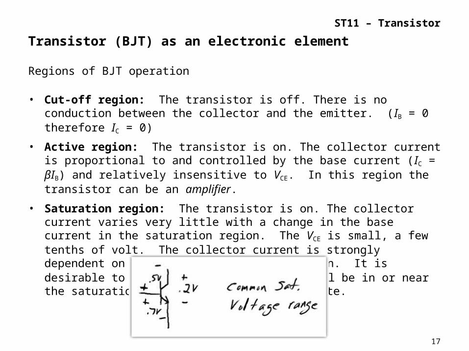
Regions of BJT operation
• Cut-off region: The transistor is off. There is no conduction between the collector and the emitter. (IB = 0 therefore IC = 0)
• Active region: The transistor is on. The collector current is proportional to and controlled by the base current (IC = βIB) and relatively insensitive to VCE. In this region the transistor can be an amplifier.
• Saturation region: The transistor is on. The collector current varies very little with a change in the base current in the saturation region. The VCE is small, a few tenths of volt. The collector current is strongly dependent on VCE unlike in the active region. It is desirable to operate transistor switches will be in or near the saturation region when in their on state.

18
ST11 – Transistor
Transistor (BJT) as an electronic element
Rules for Bipolar Junction Transistors (BJTs):• For an npn transistor, the potential at the collector VC must be
greater than the potential at the emitter VE by at least a few tenths of a volt; otherwise, current will not flow through the C-E junction, no
matter what the applied voltage at the base.
• For the npn transistor, there is a voltage drop from the base to the emitter of 0.6 V. In terms of operation, this means that the base voltage VB of
an npn transistor must be at least 0.6 V greater that the emitter voltage VE; otherwise, the transistor will not pass emitter-to-collector current.
19
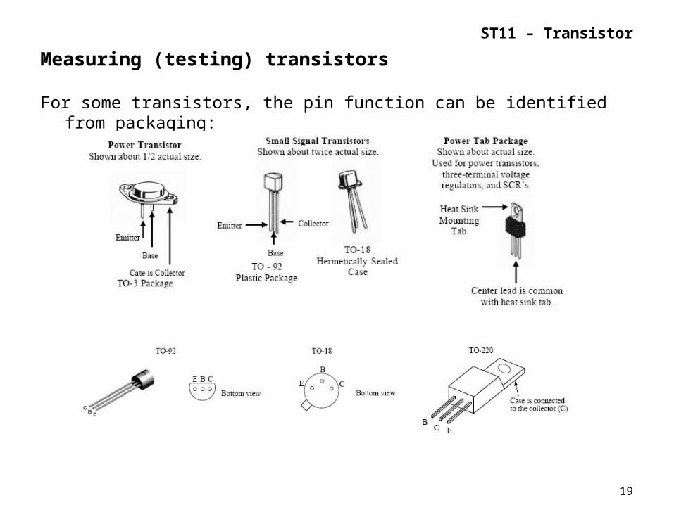
ST11 – Transistor
Measuring (testing) transistors
For some transistors, the pin function can be identified from packaging:
20
ST11 – Transistor
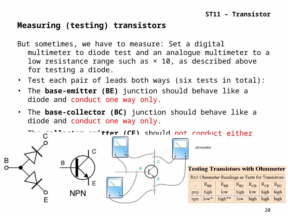
Measuring (testing) transistors
But sometimes, we have to measure: Set a digital multimeter to diode test and an analogue multimeter to a low resistance range such as × 10, as described above for testing a diode.
• Test each pair of leads both ways (six tests in total): • The base-emitter (BE) junction should behave like a diode and
conduct one way only.
• The base-collector (BC) junction should behave like a diode and conduct one way only.
• The collector-emitter (CE) should not conduct either way.
21
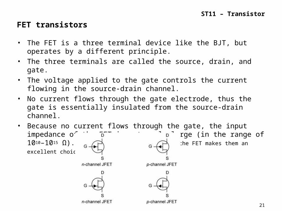
ST11 – Transistor
FET transistors
• The FET is a three terminal device like the BJT, but operates by a different principle.
• The three terminals are called the source, drain, and gate. • The voltage applied to the gate controls the current flowing in the
source-drain channel. • No current flows through the gate electrode, thus the gate is
essentially insulated from the source-drain channel. • Because no current flows through the gate, the input impedance
of the FET is extremely large (in the range of 1010–1015 Ω). The large
input impedance of the FET makes them an excellent choice for amplifier inputs.

22
ST11 – Transistor
Transistor construction
• Transistors, like diodes, are produced using a variety of chemical processes.

23
ST11 – Transistor
Basic circuits
•
We used a circuit like this to discuss transistor properties
– but there are no resistances in neither look A nor loop B – short circuit!
So, this is not a practical example....
Using a single resistor in the emitter is a practical example, but not interesting for us:
- since it cannot give any voltage amplification:
Vi - Vbe = Vo
24
ST11 – Transistor
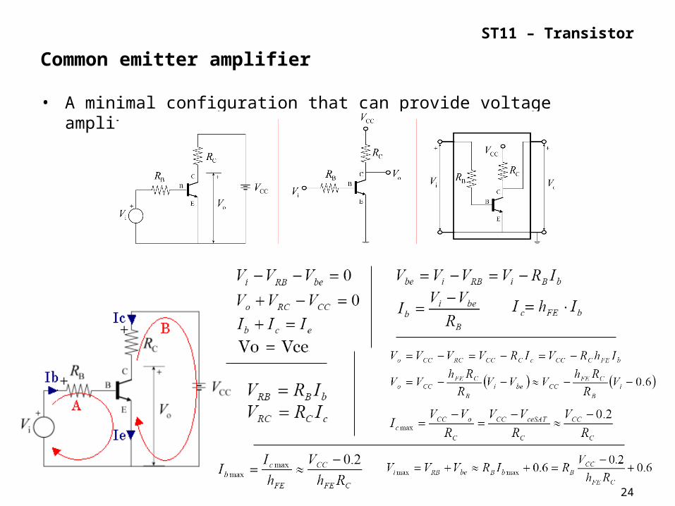
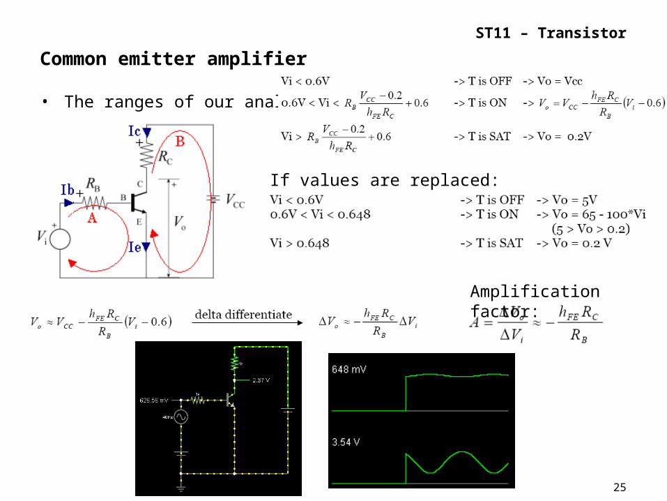
Common emitter amplifier
• A minimal configuration that can provide voltage amplification
25
ST11 – Transistor
Common emitter amplifier
• The ranges of our analysis:
If values are replaced:
Amplification factor:

26
ST11 – Transistor
Common emitter amplifier
• For practical applications, this simplest form of the common emitter amplifier is rarely used; something like below is more common:
• common emitter amplifier also has equivalent input resistance (looking into the base):
– Multiplied by factor beta

27
ST11 – Transistor
Current source and current mirror
• Current source – simply polarize CE amplifier
Current mirror

28
ST11 – Transistor
Astable multivibrator
• an oscillator circuit, that generates a pair of complementary square-wave voltages. As such, it also be seen as a digital clock - or more generally, switching, or logic circuit
• Only one transistor can conduct at a time• When supply voltage, VCC is applied, one
transistor will conduct more than the other due to some circuit imbalance.
• Q1 is conducting (ON) and Q2 is cut-off (OFF). – C1 charges exponentially with t=R1C1 towards the supply voltage
through R1 → VB2 also increases exponentially towards VCC.(VC1=0.2)
– When VB2 crosses the coupling voltage, Q2 starts conducting and VC2 falls to VCESAT → VB1 falls due to capacitive coupling between collector of Q2 and base of Q1 → driving Q1 into OFF state.
– Now Q1 OFF and Q2 ON – the process repeats
29
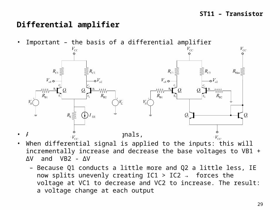
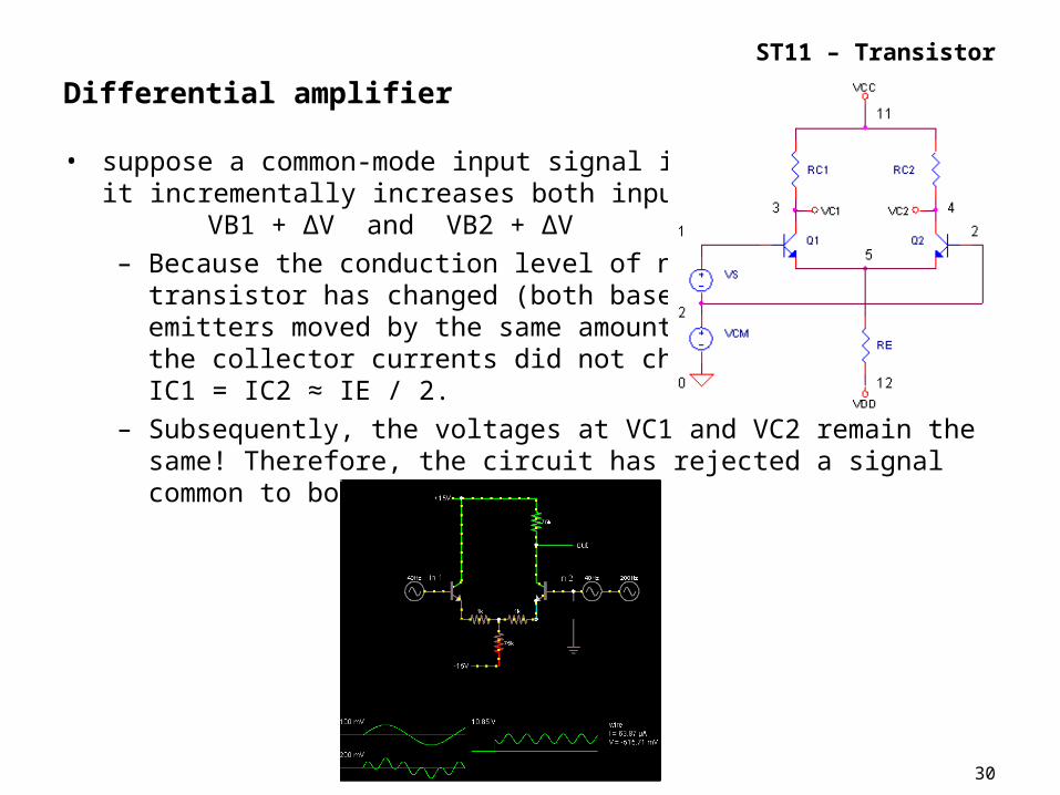
ST11 – Transistor
Differential amplifier
• Important – the basis of a differential amplifier
• Amplifies differential signals, rejects common signals• When differential signal is applied to the inputs: this will incrementally
increase and decrease the base voltages to VB1 + ΔV and VB2 - ΔV – Because Q1 conducts a little more and Q2 a little less, IE now
splits unevenly creating IC1 > IC2 → forces the voltage at VC1 to decrease and VC2 to increase. The result: a voltage change at each output
30
ST11 – Transistor
Differential amplifier
• suppose a common-mode input signal is applied: it incrementally increases both inputs to
VB1 + ΔV and VB2 + ΔV– Because the conduction level of neither
transistor has changed (both bases and emitters moved by the same amount), the collector currents did not change.IC1 = IC2 ≈ IE / 2.
– Subsequently, the voltages at VC1 and VC2 remain the same! Therefore, the circuit has rejected a signal common to both inputs.

31
ST11 – Transistor
Sensing application - Phototransistor
• A phototransistor is in essence nothing more than a bipolar transistor that is encased in a transparent case, so that light can reach the base-collector junction. – The phototransistor works like a photodiode, but with a much
higher sensitivity for light, because the electrons that are generated by photons in the base-collector junction are injected into the base, and this current is then amplified by the transistor operation.
– However, a phototransistor has a slower response time than a photodiode.