SRT Division: Architectures, Models, and...
27
SRT Division: Architectures, Models, and Implementations David L. Harris, Stuart F. Oberman, and Mark A. Horowitz Computer Systems Laboratory Stanford University Stanford, CA 94305 harrisd, horowitz @leland.stanford.edu, [email protected] September 9, 1998
Transcript of SRT Division: Architectures, Models, and...
SRT Division: Architectures, Models, and Implementations
David L. Harris, Stuart F. Oberman, and Mark A. Horowitz
Computer Systems LaboratoryStanford UniversityStanford, CA 94305
fharrisd, [email protected], [email protected]
September 9, 1998

Abstract
SRT dividers are common in modern floating point units. Higher division performance is achieved byretiring more quotient bits in each cycle. Previous research has shown that realistic stages are limited toradix-2 and radix-4. Higher radix dividers are therefore formed by a combination of low-radix stages.In this paper, we present an analysis of the effects of radix-2 and radix-4 SRT divider architecturesand circuit families on divider area and performance. Using analytical modeling and simulation, weevaluate the performance and area of a wide variety of divider architectures and implementations. Weconclude that divider performance is only weakly sensitive to reasonable choices of architecture but issignificantly improved by aggressive circuit techniques.
1 Introduction
A simple and widely implemented class of division algorithm is digit recurrence. The most common
implementation of digit recurrence division in modern microprocessors is SRT division, taking its name
from the initials of Sweeney, Robertson [1] and Tocher [2], who developed the algorithm independently
at approximately the same time. SRT division uses subtraction as the fundamental operator to retire
a fixed number of quotient bits in each iteration. Two fundamental works on SRT division are those
of Atkins [3], the first major analysis of SRT algorithms, and Tan [4], a derivation of high-radix SRT
division and an analytic method of implementing SRT look-up tables. Ercegovac and Lang [5] provide a
comprehensive treatment of the theory of SRT division and square root. Although division is typically an
infrequent operation, ignoring its implementation significantly degrades system performance for many
applications [6].
Various techniques have been proposed for increasing division performance, including cascading sim-
ple low-radix stages, overlapping sections of one stage with another stage, and prescaling the input
operands [7]. All of these methods introduce area-performance tradeoffs. Ercegovac and Lang [5] ana-
lyze the tradeoffs of using several of these optimizations in the context of static CMOS standard-cells.
Williams [8] presents a self-timed dynamic CMOS divider comprising a ring of five radix-2 stages that
incorporates several of these techniques, and he also presents an analysis of the performance and area
effects of the architectural components. Prabhu [9] presents the tradeoffs encountered when designing
the Sun UltraSparc radix-8 divider.

In contrast to previous works, this paper analyzes in detail the effects of both circuit style and divider
architecture on the performance and area of divider implementations. We present the performance re-
sults using the technology-independent metric of fanout-of-4 inverter delay. We therefore are able to
extrapolate our results to future process technologies. While the discussion here is devoted to division,
the theory of square root computation is an extension of the theory of division. Accordingly, most of the
analyses presented here can also be applied to the design of square root units.
We survey the fundamental design parameters of SRT division and present the most common tech-
niques for achieving higher performance in Section 2. Realizing the performance benefits of good circuit
techniques, we examine circuit issues relating to dual-rail domino divider implementations in Section 3.
Using the principles of logical effort, we develop in Section 4 an analytical model of divider speed that
includes both intrinsic gate delays and the branching effort of parallel architectures. The model shows
that some amount of quotient selection overlap is important, but that other architectural choices such
as radix make little difference. Area and simulated performance results for a wide variety of divider
architectures and circuit styles in Section 5 confirm the model’s predictions. We conclude in Section 6
that fast SRT dividers should be built from domino circuits using any of several reasonable architectures
to achieve speeds of 3.5-5 fanout-of-4 inverter delays per quotient bit.
2 Architectures
2.1 Definitions
Computer division by digit recurrence is similar to long division learned in elementary school. The
partial remainder is initially set to the dividend. On each step, the divisor is compared to the partial
remainder to produce a quotient digit. The quotient digit is multiplied by the divisor and subtracted
from the partial remainder; the result is then shifted by one position to form a new partial remainder.
Elementary school students use the quotient digit set f�� ���� �g, corresponding to radix 10. Computers
often use radix 2 or radix 4. One step is required for each quotient digit. To analyze the latency of
division, we must define the format of the operands and the range of each quotient digit.
In this analysis, the input operands are assumed to be represented in a normalized floating point format
2

with n bit significands in sign-and-magnitude representation. The algorithms presented here are applied
only to the magnitudes of the significands of the input operands. Computing the resulting exponent and
sign is straightforward. The most common format found in modern computers is the IEEE 754 standard
for floating point arithmetic. This standard defines single and double precision formats, where n=24
for single precision and n=53 for double precision. The significand consists of a normalized quantity,
with an explicit or implicit leading bit to the left of the implied binary point, and the magnitude of the
significand is in the range [1,2). However, to simplify the presentation, this analysis assumes fractional
quotients normalized to the range [0.5,1).
A division step which produces b bits of quotient is defined to be radix-r where:
r � �b (1)
Therefore, an n bit division using radix-r requires k steps:
k �n
b(2)
If each step takes one cycle, such an algorithm has a latency of k cycles. The cycle time of the
divider is defined as the maximum time to compute one iteration of the algorithm. Depending upon the
implementation, this may or may not be the same as the cycle time of the processor.
We can now formally define the steps of division. We set the initial partial remainder P� to the
dividend. On step j, we compute the next quotient digit qj�� by comparing multiples of the divisor D to
the current partial remainder:
qj�� � SEL�Pj� D� (3)
We then find the next partial remainder Pj�� by subtracting the selected divisor multiple from the current
partial remainder and shifting the difference:
Pj�� � r�Pj � qj��D� (4)
3

The final quotient after k iterations is the weighted sum of the quotient digits:
q �kX
j��
qjr�j (5)
2.2 SRT Divider Parameters
To perform fast division, we would like an algorithm which has a low latency (in cycles) and a short
cycle time. The latency is set by the radix r; higher radicies offer lower latencies. The cycle time is
set by the operations occurring in each cycle: quotient digit selection and partial remainder generation.
The simplest form of division, like that taught in elementary school, uses nonredundant quotient digits
and partial remainder representations. This technique requires the quotient selection logic to exactly
compare the partial remainder and divisor using a slow n-bit subtraction. An n-bit subtraction is also
required to find the next partial remainder.
The key idea of SRT division is to guess the quotient digit based on a few of the most significant
divisor and partial remainder bits, rather than computing it exactly. As long as the guess is close enough,
the algorithm can correct on subsequent steps using redundant quotient digits. For example, a radix 2
quotient selection function could be built which guesses digits that are either correct or slightly too high.
If a quotient digit set of f��� �� �g instead of just f�� �g is used, the -1 digit can correct on a later step
for an incorrect guess in a previous step.
Now quotient digit selection is faster because it only involves a few most significant bits rather than all
n. To take advantage of this speedup, we must also improve partial remainder formation so that an n-bit
subtraction is not required on each step. This can be done by keeping the partial remainder in redundant
form such as P = Ps + Pc. The next redundant partial remainder can then be computed in a single gate
delay using a (3,2) carry-save adder which sums Ps, Pc, and �qD.
We will consider SRT division algorithms which use redundant quotient digits and partial remainder
representations to avoid the slow n-bit subtractions. The two important divider parameters are the radix
and the set of redundant quotient digits.
4

2.2.1 Choice of Radix
To minimize latency, as measured in cycles, we would like to use a high radix r. However, low latency
does not come for free. As the radix increases, the quotient-digit selection becomes more complicated,
which may increase the cycle time. Moreover, the generation of all required divisor multiples may
become impractical for higher radices. Oberman [10] shows that the delay of quotient selection tables
increases linearly with increasing radix, while the area increases quadratically. While prescaling of
the input operands [11] reduces table complexity at the expense of additional latency, the difficulty in
generating all divisor multiples for radix-8 and higher limits practical divider implementations to radix-2
and radix-4.
2.2.2 Choice of Quotient Digit Set
For a given choice of radix r, some range of digits is chosen for the allowed values of the quotient in
each iteration. The nonredundant case is where, for radix r, there are exactly r allowed values of the
quotient. However, to increase the performance of the algorithm, a redundant digit set is used. Such
a digit set is composed of symmetric signed-digit consecutive integers, where the maximum digit is
a. The digit set is made redundant by having more than r digits in the set. By using a larger number
of allowed quotient digits, the complexity and latency of the quotient selection function is reduced
because the later steps can correct for larger inaccuracies in the guess of the quotient digit. However,
choosing a smaller number of allowed digits for the quotient simplifies generation of the multiples of the
divisor. Specifically, for radix-2, the digit set is f��� �� �g. For radix-4, there are two typical choices for
the digit set: minimally redundant f������ �� �� �g and maximally redundant f��������� �� �� �� �g.
The quotient selection logic for a maximally-redundant radix-4 digit set is about 20% faster and 50%
smaller than for a minimally-redundant digit set [10]. However, maximally-redundant radix-4 requires
the computation of the 3x divisor multiple, which typically requires extra initial delay and area.
5

Datapath
Control
Block 1Datapath
Block mDatapath
Block 1Control
Block mControl
...
...
Input Mux &
Latch
Figure 1. SRT divider block diagram
2.3 Higher Performance
Several techniques have been proposed for improving the performance of SRT division, but most in-
volve cascading low-radix stages to form a higher radix divider. The primary problem with a cascade
of stages is the proportional increase in cycle time. To avoid this increase, some computation can pro-
ceed in parallel at the expense of area. Taylor [12] proposes overlapping the quotient-digit selection of
consecutive stages. Oberman [10] and Quach [13] discuss overlapping remainder computation. Fan-
drianto [14] discusses a cascade of lower radix segments in which there is no shifting of the partial
remainder between the segments through the use of range reduction. In this study, we analyze the effects
of five overlap schemes: no overlap, overlapped quotient selection, overlapped remainder computation,
overlapped quotient and remainder computation, and a hybrid overlap scheme.
A general divider organization using overlapping is shown in Fig. 1. This floorplan is divided into
a control section for quotient digit computation that typically operates on a small number of the most
significant bits (about 4 for radix-2 and 8 for radix-4), and a datapath section for partial remainder
formation of the remaining significand bits.
The divider is defined to comprise a cascade of m blocks, where each block has a delay of tblock. Each
block is composed of s overlapped radix-r stages. The divider therefore retires b� � m � s � b bits in
each cycle, with a total cycle time of m � tblock toverhead, where toverhead includes latch delay, clock
skew, and the input multiplexor for injecting new operands. Such an overlapped scheme produces k �
radix-r� digits with
r� � �b�
(6)
k� �n
b�(7)
6

CSA
QSLC
{aD, ..., -aD}
PR[i]
PR[i+1]
q[i+1]
Control
Datapath
Figure 2. Non-overlapped design
The overlap schemes we consider are illustrated in Figs. 2 through 6. The critical path(s) are indicated
by the heavy black lines. Although partial remainders are stored in carry-save form, they are drawn with
a single line for simplicity. The architectures are shown overlapping two stages, but can be generalized
to higher overlap [9].
2.3.1 Non-overlapped
A simple non-overlapped design is common in low-cost applications, such as the Intel Pentium Proces-
sor [15]. A block diagram is shown in Fig. 2. The quotient selection logic (QSLC) guesses the quotient
digit q[i+1] based on the most significant bits of the current partial remainder PR[i] and the divisor. The
result is buffered and driven across the datapath to select the appropriate divisor multiple, which is then
subtracted from the partial remainder and shifted to form the next partial remainder PR[i+1]. Subtrac-
tion is performed in redundant form using the carry-save adder (CSA). Since the fixed shift involves only
wire, the critical path delay is:
tblock � tqslc tbuf tmux tcsa (8)
2.3.2 Overlapping Quotient Selection
Overlapping quotient selection (Fig. 3) requires additional control logic but no additional datapath ele-
ments. This technique was demonstrated by Taylor [12]. The critical path involves speculatively gener-
7
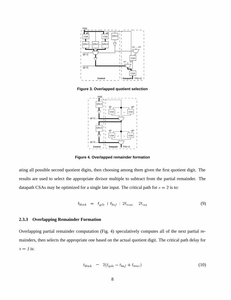
QSLC
CSA
QSLC QSLC
CSA QSLC
CSA
... ...{aD, ..., -aD}
{aD, ..., -aD}
PR[i]
PR[i+2]
q[i+1]
q[i+2]
aD -aD
Control Datapath
CSA
Figure 3. Overlapped quotient selection
QSLC
CSA CSA
CSA CSA
... ...
... ...
PR[i]
PR[i+2]
q[i+1]
q[i+2]
aD -aD
aD -aD
Control Datapath
QSLC
Figure 4. Overlapped remainder formation
ating all possible second quotient digits, then choosing among them given the first quotient digit. The
results are used to select the appropriate divisor multiple to subtract from the partial remainder. The
datapath CSAs may be optimized for a single late input. The critical path for s � � is to:
tblock � tqslc tbuf �tmux �tcsa (9)
2.3.3 Overlapping Remainder Formation
Overlapping partial remainder computation (Fig. 4) speculatively computes all of the next partial re-
mainders, then selects the appropriate one based on the actual quotient digit. The critical path delay for
s � � is:
tblock � ��tqslc tbuf tmux� (10)
8
QSLC
CSA
QSLC QSLC
QSLC
CSA CSA
CSA CSA
... ... ... ...
... ...
PR[i]
PR[i+2]
q[i+1]
q[i+2]
aD -aD
aD -aD
aD -aD
Control Datapath
CSA
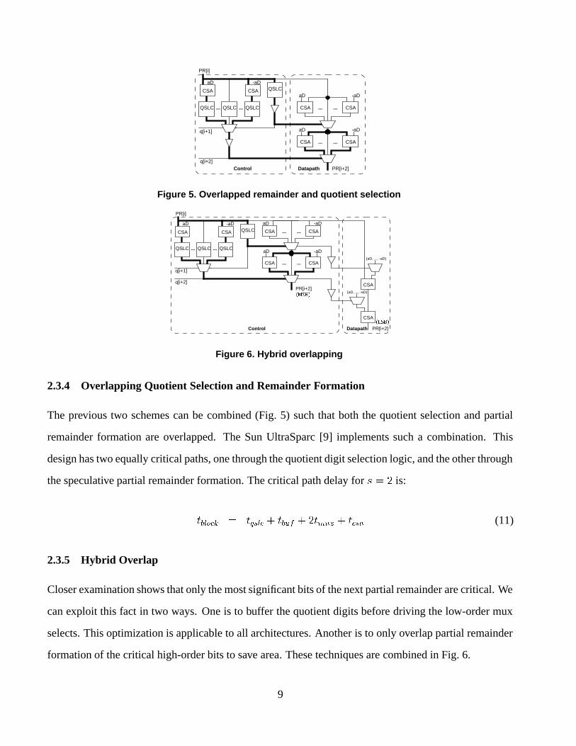
Figure 5. Overlapped remainder and quotient selection
QSLC
CSA
QSLC QSLC
QSLC CSA CSA
CSA CSA
... ...
... ...
... ...
PR[i]
PR[i+2]
q[i+1]
q[i+2]
aD -aD aD -aD
aD -aD
Control
CSA
CSA
{aD, ..., -aD}
{aD, ..., -aD}
PR[i+2]Datapath
CSA
Figure 6. Hybrid overlapping
2.3.4 Overlapping Quotient Selection and Remainder Formation
The previous two schemes can be combined (Fig. 5) such that both the quotient selection and partial
remainder formation are overlapped. The Sun UltraSparc [9] implements such a combination. This
design has two equally critical paths, one through the quotient digit selection logic, and the other through
the speculative partial remainder formation. The critical path delay for s � � is:
tblock � tqslc tbuf �tmux tcsa (11)
2.3.5 Hybrid Overlap
Closer examination shows that only the most significant bits of the next partial remainder are critical. We
can exploit this fact in two ways. One is to buffer the quotient digits before driving the low-order mux
selects. This optimization is applicable to all architectures. Another is to only overlap partial remainder
formation of the critical high-order bits to save area. These techniques are combined in Fig. 6.
9

This architecture is a hybrid of the overlapped quotient selection and remainder formation design for
the critical bits and the overlapped quotient selection design for the non-critical bits. The quotient digits
are buffered before driving the non-critical least significant bits in the datapath. This eliminates the
buffer delay from the critical path to the high order bits. The critical path delay for s � � is:
tblock � tqslc �tmux tcsa (12)
Hardware is saved relative to designs which overlap partial remainder formation because no specula-
tive adders are needed in the datapath for partial remainder formation. The non-critical partial remainder
bits lag behind the critical bits by the delay of a buffer plus CSA. This may slightly increase the time
required for rounding and normalization at the end of a divide. More importantly, the non-critical bits
must catch up before they are required by quotient selection. Therefore, the speculative partial remain-
der formation must operate on s � b extra bits to catch these bits up before they become critical. The
lag of the non-critical bits plus the delay through the partial remainder formation must be less than the
delay of the critical quotient selection path so that the non-critical bits catch up as they are shifted into
the critical portion. Specifically, the critical path delay from q[i+2] to PR[i+4] through the quotient digit
logic to generate the next set of most-significant partial remainder bits is:
tcrit � tmux �tcsa tqslc tmux tmux� (13)
while the sum of the lagging path delay and partial remainder formation delay is:
tnoncrit � �tbuf tmux tcsa� (14)
�tcsa tmux tcsa tmux�
Simplifying, to keep tnoncrit � tcrit,
tbuf �tcsa � tqslc (15)
10

# Wide # Wide #Architecture Block Latency # QSLC CSAs MUXes BitlinesNon-overlapped s�tqsel tbuf tmux tcsa� s s s aOverlap PR s�tqsel tbuf tmux� s �as s � aOverlap QS tqsel tbuf stmux stcsa see Table 2 s s aOverlap PRQS tqsel tbuf stmux �s� ��tcsa see Table 2 �as s � aHybrid overlap tqsel stmux �s� ��tcsa see Table 2 s s a
Table 1. Comparison of architectures
As we show later, quotient selection is the most time consuming component, especially for radix-4
designs. Therefore, it is reasonable to expect this constraint to be satisfied, especially since the datapath
CSA may be optimized for a single late input. If quotient selection is too fast, the final partial remainder
formation can be overlapped in the datapath, adding more CSAs, but relaxing the timing constraint from
Eq 15 to tbuf tcsa � tqslc.
2.4 Comparison
Table 1 compares the latency, hardware cost, and wiring of each architecture. The number of QSLCs,
which dominate control area, and number of CSAs and MUXes in the datapath are listed. Also, the
number of metal tracks required is computed (see Fig. 7). Overlapping quotient digit selection saves
s � � quotient selection and buffer delays at the expense of additional quotient selection logic blocks.
Overlapping partial remainder formation saves the delay of one CSA at the expense of many more CSAs
performing speculative computation. Finally, the hybrid scheme eliminates the buffer delay and also
avoids a large number of speculative CSAs. From Table 1, the hybrid overlapping scheme has the lowest
latency and also saves hardware relative to the next fastest scheme. However, the performances of other
architectures that overlap quotient selection are within a CSA and buffer delay of the hybrid scheme,
and as discussed previously, the buffer may be optimized out of the critical path.
The number of quotient selection blocks increases sharply when moving from radix-2 to radix-4 and
for increasing s, as shown in Table 2. Due to the exponential area increase with degree of overlap,
reasonable designs are limited to an overlap of s � � or possibly s � �.
11

s r � � a � � r � � a � � r � � a � �1 1 1 12 4 6 83 11 27 394 26 112 166
Table 2. QSLCs for overlapped architectures
3 Circuits
Overlapping stages is important, but Table 1 shows that the incremental improvement of better overlap
techniques is small. Execution unit designers are therefore turning to more aggressive circuit techniques,
especially domino circuits, to greatly reduce latency [16].
Three key circuit issues which impact architectural choices are domino monotonicity requirements,
wiring cost, and clocking overhead. Designers accustomed to static logic must remember that domino
circuits require monotonically rising inputs during evaluation. Since single-rail domino circuits are not
a functionally complete logic family, non-monotonic gates such as CSAs require dual-rail inputs and
outputs to code both true and complementary signals. This increases the area of logic gates and the
amount of interconnect. Radix-4 quotient selection logic is especially impacted because it is relatively
large. Fortunately, the quotient digits are consumed only by multiplexors, so they can be computed in
single-rail 1-hot form. Two options for fast QSLCs are domino gates and dynamic self-timed PLAs. We
found that radix-4 minimally/maximally redundant 1-hot PLAs have 50/25 minterms respectively, while
according to [10] minimally/maximally redundant Gray-encoded PLAs have only 25/14 minterms. Static
designs can implement either a 1-hot PLA or an encoded PLA to save area, but domino implementations
require the larger 1-hot design.
The datapath dominates the area of most dividers, so we must examine the number of bitlines running
between elements within a bitslice. Dynamic designs double the wire count because dual-rail signals
are needed. All floating point blocks have fixed overhead of power, ground, and three data busses: two
inputs and one output. Dividers have many additional bitlines because partial remainders are kept in
redundant form.
12

22
2
a
PR[i+1]PR[i]
PR feedback
{D, 2D, ..., aD}
qD
MUX CSA
22
2
aq[i+1]D
2 PR[i+2]
PR feedback
{D, 2D, ..., aD}
PR[i]
MUX CSA MUX CSA
PR[i+1]
2
2
a
q[i+1]D 2
MUXCSA MUXMORECSAs
PR[i+1]
CSA CSA MORECSAs
CSA
q[i+2]D 2
q[i+2]D
2 2 PR[i+2]
PR feedback
{D, 2D, ..., aD}
PR[i]
Non-Overlap (s=1) Overlap QS / Hybrid (s=2)
Overlap PRF / Overlap QS & PRF (s=2)
Figure 7. SRT datapath floorplan for one block
Fig. 7 illustrates wiring requirements on a floorplan of a block for various architectures. A dot on a
wire over an element indicates that the signal is used in that element. On all architectures, two lines are
required for driving the redundant partial remainder along the path and another two lines are required
for feeding the result back to the next iteration. Furthermore, divisor multiples must be driven to all of
the blocks. Although there are �a � divisor multiples, we must only transmit the a positive multiples
and can generate the negative multiples with a local inversion. Finally, the appropriate divisor must
be selected. In architectures which do not speculatively generate partial remainders, only one wire
is required to drive the divisor mux output to the CSA which generates the next partial remainder. In
speculative architectures, �a CSAs generate two bits of output each. It would seem �a wires are required
as input to the divisor mux. However, by distributing the multiplexor legs across the adders, only two
wires are needed for the redundant result.
A static divider requires either a or � a bitlines, which poses little difficulty. A dual-rail domino
divider requires twice as many bitlines. These bitlines can be accommodated in a bit pitch of about
120�, where � is half of the minimum drawn transistor length. Cells can be efficiently laid out at this
pitch, so wire limitations are not expected to increase divider area significantly in a process with 3 or 4
metal layers. This is consistent with [8] which reports only a 15% area penalty for dual-rail domino in a
2 layer process.
Clocking overhead is important in both static and dynamic designs. Static designs conventionally use
a flip-flop with a multiplexor at the beginning of the cycle to capture either a new divider input or the
result of the previous iteration. The flip-flop adds a delay of tclk�q tsetup tskew to the path, which
13
can be large. Textbook domino designs require latches between phases of domino logic and are also
sensitive to clock skew, but skew-tolerant domino techniques [17] make domino much more attractive
by eliminating latch delays and clock skew from the critical path. Good domino designs must only pay
the cost of one 2:1 multiplexor at the beginning of each cycle. This cost may be amortized over many
bits produced in the cycle.
Since the area is proportional to the number of blocks, area can be reduced without impacting latency
by clocking the divider at a higher frequency than the rest of the processor. For example, the HP-PA7100
[18] achieves higher radix by clocking a lower radix core at double frequency. This technique improves
area at the expense of the complexity of generating a higher frequency clock.
In summary, domino is an attractive approach for high-performance dividers. It greatly reduces gate
delays and eliminates much of the clocking overhead found in flip-flop-based static designs. The domino
wiring requirements do not significantly increase area in processes with 3 or more metal layers. Thus, the
primary costs of domino designs are the extra area consumed by quotient selection logic, the increased
power consumption while the divider is active, and the necessary circuit design expertise.
4 An Analytical Model for Divider Delay
The analysis of architectures explores the elements in each critical path and suggests that certain
architectures may be faster than others because they have fewer gates in the critical paths. However,
critical path delay is a strong function of the loading each gate must drive as well as the number of gates.
This section develops a more powerful model based on the principles of logical effort to compare the
delay of dividers. The model is calibrated with simulations of a few building blocks and predicts the
performance of a wide variety of architectures. An important limitation of the model is that it neglects
wiring capacitance and thereby underestimates the delay of highly parallel architectures with lengthy
wires.
14
4.1 Logical Effort
The delay of a CMOS gate depends on the intrinsic delay of the gate driving its internal parasitics, on
the load that must be driven, and on the effective resistance of the gate. This can be modeled as:
t � tint rf (16)
where tint is the intrinsic delay, f is the fanout, defined asCload�Cin, and r is proportional to the effective
resistance of the gate. More complex gates have larger tint and r terms.
Sutherland [19] defines the logical effort LE of a gate to be the ratio of its effective resistance to that
of an inverter with the same input capacitance. The gain g of the gate can then be defined as the fanout
multiplied by the logical effort. Now the delay can be rewritten in terms of the gain of each gate.
LE � rgate�rinv (17)
g � LE � f (18)
t � tint grinv (19)
The gain G of an entire path is the product of the gains of each stage. This gain comes from the logical
effort of each stage, the overall fanout of the path, and any branching within the path. The overall fanout
F is defined as Cload�Cin of the path. The branching factor B accounts for other loads within the path;
for example, a path from computing a multiplexor select to the data output of one bit of a 64 bit mux has
B � �� because 63 other multiplexor bits must be driven. In summary, a path with � stages has:
G � BF�Y
i��
LEi (20)
It can be shown that the delay of a path is minimized when gates are sized such that each stage has
equal gain. The minimum path delay therefore is the sum of the gain-dependent delay, which is equal
15

per stage, plus the intrinsic delays of each stage.
tpath � �rinv�
pG
�X
i��
tint�i (21)
4.2 Critical Paths
The delay of various architectures can now be modeled using the logical efforts and intrinsic delays of
each stage and the branching effort and fanout of the path. Since each divider block drives an identical
divider block, path fanout is always 1 and will be ignored. This section analyzes architectures to find the
components in the critical path and the overall branching effort of the path. The next section describes
simulations used to extract logical efforts and intrinsic delays of each component.
The delay of CSAs and multiplexors depends on which inputs are critical. A CSA with a single
critical input can be fast if the sum and carry results are speculatively computed for both possible values
of the critical input, then simply selected when the critical input arrives. A CSA with two critical inputs
cannot use this optimization. Similarly, a multiplexor can be optimized for late control inputs, late data
inputs, or simultaneously arriving control and data. To capture these optimizations, elements are defined
as CSA1, CSA2, MUXC, MUXD, and MUXB, corresponding to CSAs with 1 and 2 late inputs and
multiplexors that are control-critical, data-critical, or both control and data critical.
Branching effort of a path depends on operand width, n, range of quotient digits, a, and amount
of overlapping, s. Although overlapped architectures compute with slightly more than n bits, n is a
convenient and simple estimate. Consider the fanout of each architecture in more detail.
Non-overlapped dividers have branching effort of n to drive the divisor selection mux in the datapath.
Dividers using overlapped partial remainder formation have a branching effort of n each time the
quotient bit drives the divisor selection mux. Thus, overlap by two has a branching effort of n�.
Dividers using overlapped quotient selection have a branching of n driving the divisor selection mux,
times additional branching as PR[i] drives speculative quotient selection logic. Assuming non-critical
gates can be buffered sufficiently to present negligible load, each level of speculative quotient selection
16

Architecture s B QSLC CSA2 CSA1 MUXC MUXD MUXB BUFNon-overlapped 1 n 1 1 1 1Overlap PR 2 n� 2 2 2Overlap QS 2 �an 1 1 1 1 1 1Overlap QS 3 �a�n 1 2 1 1 2 1Overlap PRQS 2 �an��a �� 1 1 1 1 1Hybrid overlap 2 �az��a �� 1 1 1 1
Table 3. Branching effort and component count of divider architectures
involves branching of roughly �a. Therefore, for overlap of s the total branching effort is ��a�s��n,
which reduces to the non-overlapped case for s=1.
Dividers using both overlapped partial remainder and quotient logic with s � � have three sources
of branching. Branching of �a � occurs as PR[i] drives the speculative and non-speculative quotient
selection logic. Another branching of n occurs when the q[i+1] signal drives the divisor selection mux.
Finally, a branching of �a occurs as PR[i+1] drives the speculative partial remainder formation CSAs.
Total branching effort is therefore �an��a ��.
Hybrid overlap with s � � is identical to the case of overlapped partial remainder and quotient logic
except that the branching of n driving divisor selection muxes is reduced to branching of z driving only
a few of the most critical bits. z is the number of bits used in the control block; typical values are 6 for
radix 2, 10 for maximally redundant radix-4, and 11 for minimally redundant radix-4. Total branching
effort is therefore �az��a ��.
Table 3 summarizes the branching effort and number of each component in the critical path of various
architectures.
4.3 Calibrating the Model
Using these component counts and fanouts, the logical effort model can predict the delay of dividers.
The LE and tint terms in the model can be estimated by hand or measured from simulation. Table 4
lists the terms based on simulation of domino gates in the HP-CMOS26B 1 �m (drawn) process. To
normalize for process, all times are expressed as multiples of the delay of a fanout-of-4 (FO4) inverter.
17
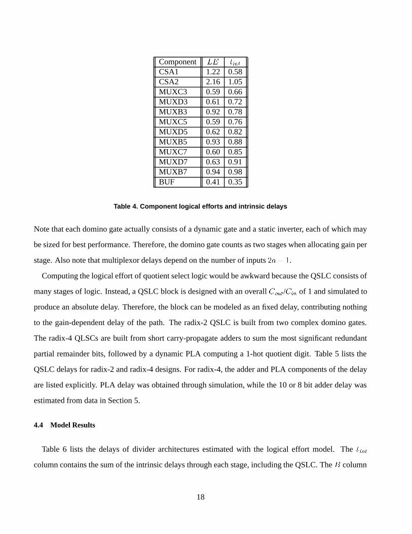
Component LE tintCSA1 1.22 0.58CSA2 2.16 1.05MUXC3 0.59 0.66MUXD3 0.61 0.72MUXB3 0.92 0.78MUXC5 0.59 0.76MUXD5 0.62 0.82MUXB5 0.93 0.88MUXC7 0.60 0.85MUXD7 0.63 0.91MUXB7 0.94 0.98BUF 0.41 0.35
Table 4. Component logical efforts and intrinsic delays
Note that each domino gate actually consists of a dynamic gate and a static inverter, each of which may
be sized for best performance. Therefore, the domino gate counts as two stages when allocating gain per
stage. Also note that multiplexor delays depend on the number of inputs �a �.
Computing the logical effort of quotient select logic would be awkward because the QSLC consists of
many stages of logic. Instead, a QSLC block is designed with an overall Cout/Cin of 1 and simulated to
produce an absolute delay. Therefore, the block can be modeled as an fixed delay, contributing nothing
to the gain-dependent delay of the path. The radix-2 QSLC is built from two complex domino gates.
The radix-4 QLSCs are built from short carry-propagate adders to sum the most significant redundant
partial remainder bits, followed by a dynamic PLA computing a 1-hot quotient digit. Table 5 lists the
QSLC delays for radix-2 and radix-4 designs. For radix-4, the adder and PLA components of the delay
are listed explicitly. PLA delay was obtained through simulation, while the 10 or 8 bit adder delay was
estimated from data in Section 5.
4.4 Model Results
Table 6 lists the delays of divider architectures estimated with the logical effort model. The tint
column contains the sum of the intrinsic delays through each stage, including the QSLC. The B column
18
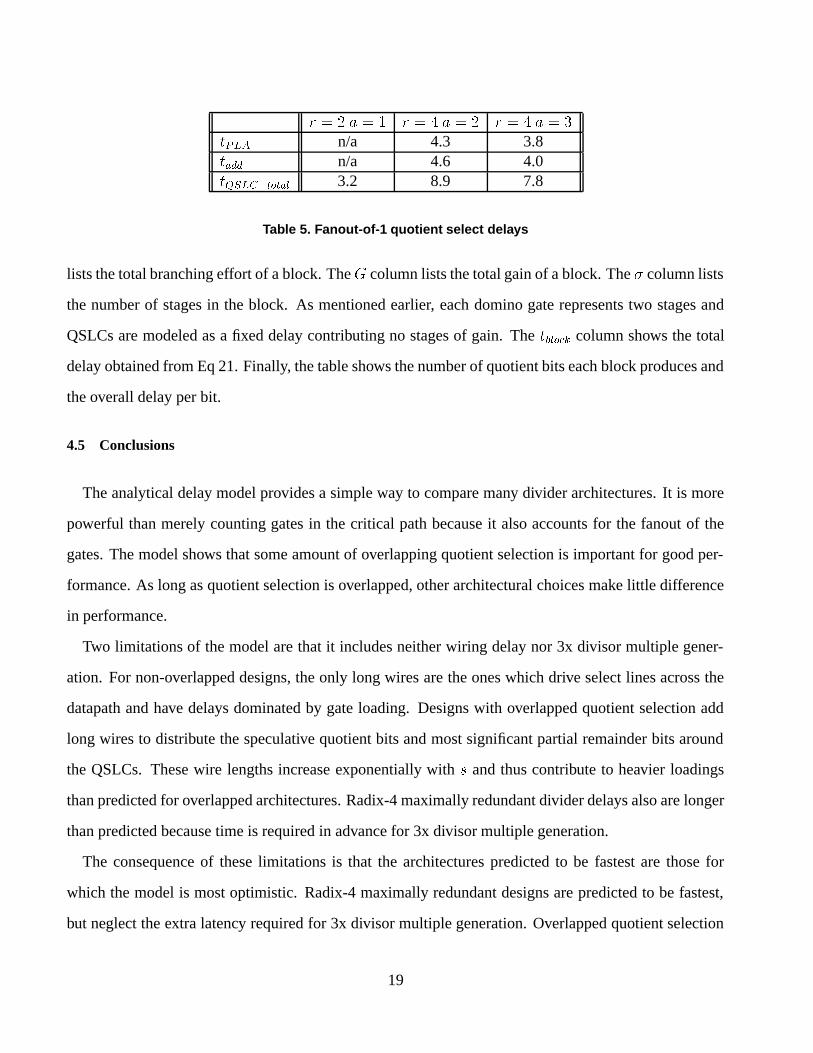
r � � a � � r � � a � � r � � a � �tPLA n/a 4.3 3.8tadd n/a 4.6 4.0tQSLC�total 3.2 8.9 7.8
Table 5. Fanout-of-1 quotient select delays
lists the total branching effort of a block. The G column lists the total gain of a block. The � column lists
the number of stages in the block. As mentioned earlier, each domino gate represents two stages and
QSLCs are modeled as a fixed delay contributing no stages of gain. The tblock column shows the total
delay obtained from Eq 21. Finally, the table shows the number of quotient bits each block produces and
the overall delay per bit.
4.5 Conclusions
The analytical delay model provides a simple way to compare many divider architectures. It is more
powerful than merely counting gates in the critical path because it also accounts for the fanout of the
gates. The model shows that some amount of overlapping quotient selection is important for good per-
formance. As long as quotient selection is overlapped, other architectural choices make little difference
in performance.
Two limitations of the model are that it includes neither wiring delay nor 3x divisor multiple gener-
ation. For non-overlapped designs, the only long wires are the ones which drive select lines across the
datapath and have delays dominated by gate loading. Designs with overlapped quotient selection add
long wires to distribute the speculative quotient bits and most significant partial remainder bits around
the QSLCs. These wire lengths increase exponentially with s and thus contribute to heavier loadings
than predicted for overlapped architectures. Radix-4 maximally redundant divider delays also are longer
than predicted because time is required in advance for 3x divisor multiple generation.
The consequence of these limitations is that the architectures predicted to be fastest are those for
which the model is most optimistic. Radix-4 maximally redundant designs are predicted to be fastest,
but neglect the extra latency required for 3x divisor multiple generation. Overlapped quotient selection
19

Architecture s tint B G � tblock Bits/block Delay/bit
r � � a � �Non-overlapped 1 4.8 53 15.6 6 6.6 1 6.6Overlap PR 2 8.4 2809 164 8 11.3 2 5.6Overlap QS 2 6.6 106 41.2 10 9.3 2 4.6Overlap QS 3 8.3 212 109 14 12.0 3 4.0Overlap PRQS 2 6.0 318 153 8 8.9 2 4.4Hybrid overlap 2 5.7 36 42.2 6 7.8 2 3.9
r � � a � �Non-overlapped 1 10.6 53 15.6 6 12.4 2 6.2Overlap PR 2 20.0 2809 164 8 22.9 4 5.7Overlap QS 2 12.5 212 83.8 10 15.4 4 3.8Overlap QS 3 14.3 848 449 14 18.4 6 3.1Overlap PRQS 2 11.9 1060 515 8 15.2 4 3.8Hybrid overlap 2 11.6 220 261 6 14.4 4 3.6
r � � a � �Non-overlapped 1 9.6 53 15.9 6 11.4 2 5.7Overlap PR 2 18.0 2809 170 8 20.9 4 5.2Overlap QS 2 11.5 318 130 10 14.6 4 3.6Overlap QS 3 13.5 1908 1060 14 17.8 6 3.0Overlap PRQS 2 11.0 2226 1110 8 14.6 4 3.6Hybrid overlap 2 10.7 420 512 6 13.9 4 3.5
Table 6. Analytical delay model predictions
with s � � also appears to be faster than overlaps of just s � � but does not account for greatly increased
wire loading. Hence, choice of architecture and radix makes even less difference than the model predicts.
A potential weakness of the designs is that some have many stages and a low gain per stage. It is
possible that by combining logic into fewer stages of more complex gates, speed could be improved.
Suppose the number of stages could be adjusted without changing the intrinsic delay or total gain of the
block. It can be shown that minimal delay occurs when the number of stages is selected to provide a
gain of e per stage. This minimal delay is no more than 10% better for radix-2 designs and 5% better for
radix-4 designs than the results in the table, so little benefit should be expected from combining stages.
Another interesting result of the model is that increasing parallelism does not always lead to higher
speed. For example, compare overlapping either just quotient selection or both quotient selection and
20

0
2
4
6
8
10
12
14
0 0.5 1
Area/Bit/Cycle (mm^2)
StaticA
B
C D
E
Del
ay/B
it (
FO
4)
Figure 8. Scatter plot of results
partial remainder formation for radix-4 designs. The delays of the two designs are equal. This is because
the adder delay saved by the more parallel design is lost to the higher branching effort paid to achieve
this parallelism.
5 Simulation Results
We assigned a divider design project in an advanced VLSI circuit class at Stanford University. Twelve
teams explored a wide variety of radix-2 and radix-4 double precision SRT divider designs using skew-
tolerant domino circuits. The designs reflect a variety of skill levels and area/performance tradeoffs. The
delay results are from HSPICE simulation, and the area estimates are based upon total transistor count
and device size. We compare these results with data on static dividers extrapolated from Ercegovac [5].
The designs are shown on a scatter plot of delay/bit vs. area/bit/divider cycle, shown in Fig. 8. The
labeled points are described further in Table 7 and represent those designs with the best performance for a
given area. The delay/bit is measured in fanout-of-4 inverter delays in the HP-CMOS26B process. Area
must be normalized by the number of bits produced per cycle because a divider can simply unroll more
blocks until the cycle is full. Area is estimated in mm� and can be converted to �� by multiplying by
21
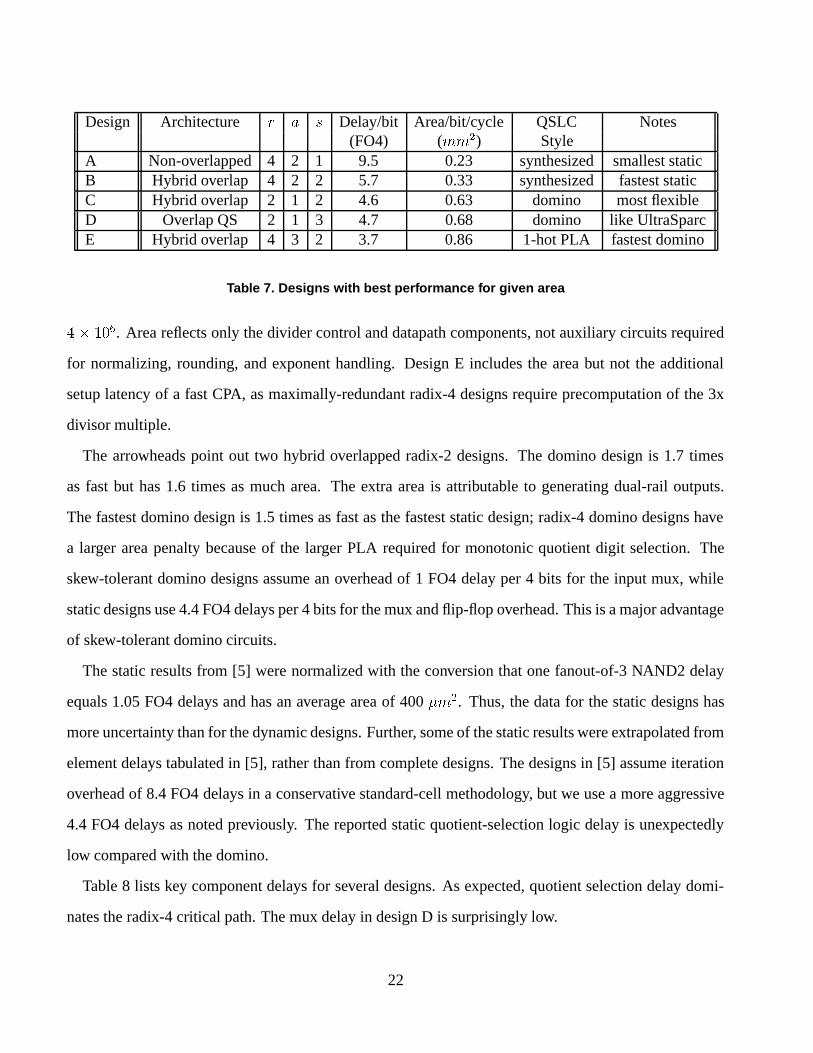
Design Architecture r a s Delay/bit Area/bit/cycle QSLC Notes(FO4) (mm�) Style
A Non-overlapped 4 2 1 9.5 0.23 synthesized smallest staticB Hybrid overlap 4 2 2 5.7 0.33 synthesized fastest staticC Hybrid overlap 2 1 2 4.6 0.63 domino most flexibleD Overlap QS 2 1 3 4.7 0.68 domino like UltraSparcE Hybrid overlap 4 3 2 3.7 0.86 1-hot PLA fastest domino
Table 7. Designs with best performance for given area
�� ���. Area reflects only the divider control and datapath components, not auxiliary circuits required
for normalizing, rounding, and exponent handling. Design E includes the area but not the additional
setup latency of a fast CPA, as maximally-redundant radix-4 designs require precomputation of the 3x
divisor multiple.
The arrowheads point out two hybrid overlapped radix-2 designs. The domino design is 1.7 times
as fast but has 1.6 times as much area. The extra area is attributable to generating dual-rail outputs.
The fastest domino design is 1.5 times as fast as the fastest static design; radix-4 domino designs have
a larger area penalty because of the larger PLA required for monotonic quotient digit selection. The
skew-tolerant domino designs assume an overhead of 1 FO4 delay per 4 bits for the input mux, while
static designs use 4.4 FO4 delays per 4 bits for the mux and flip-flop overhead. This is a major advantage
of skew-tolerant domino circuits.
The static results from [5] were normalized with the conversion that one fanout-of-3 NAND2 delay
equals 1.05 FO4 delays and has an average area of 400 �m�. Thus, the data for the static designs has
more uncertainty than for the dynamic designs. Further, some of the static results were extrapolated from
element delays tabulated in [5], rather than from complete designs. The designs in [5] assume iteration
overhead of 8.4 FO4 delays in a conservative standard-cell methodology, but we use a more aggressive
4.4 FO4 delays as noted previously. The reported static quotient-selection logic delay is unexpectedly
low compared with the domino.
Table 8 lists key component delays for several designs. As expected, quotient selection delay domi-
nates the radix-4 critical path. The mux delay in design D is surprisingly low.
22

Design tqslc tmux tcsa tbufA,B 11.3 1.9 2.3 1.8C 4.0 1.5 1.5 NAD 3.6 0.9 1.5 1.1E 7.8 1.7 - 2.6 1.7 NA
Table 8. Selected component delays (FO4)
For comparison, Williams [8] reports delays of overlapped quotient selection for radix-2 and radix-4
stages in terms of FO1 inverter delay. Converting these delays using 1 FO4 � 2.5 FO1 delays, we find
a delay per bit of 4.7 FO4 for radix-2 and 4.5 FO4 for radix-4. These are consistent with the delays
reported in this study. Comparing area is more difficult, as Williams’ self-timed ring is constrained to
overlapping of s � stages to hide the overhead of self-timing.
6 Conclusions
This study has investigated a wide range of SRT division designs. An analytical model based on
the principles of logical effort allows rapid comparison of many divider architectures. The model also
shows that it is essential to consider branching effort when evaluating architectures because time saved
by eliminating a gate in a parallel architecture may be lost to the increased branching effort required to
achieve the parallelism.
Simulation results are somewhat slower than the analytical model predicts, but still are within 20%
and are consistent in their conclusions. The speed differences can be attributed to the fact that the model
neglects loading from wires and from non-critical branches and that the simulations were done under
time pressure and may not be thoroughly optimized.
Both the model and simulation results show that using an architecture which overlaps quotient se-
lection improves speed, but that other overlapping details and especially the choice of either radix-2 or
radix-4 make little difference in overall performance. Indeed, the architectures which the model predicts
are best are also those for which the model is most optimistic. Three examples of reasonable architec-
tures which provide high performance with modest areas are hybrid overlapped radix-2 (s � �), quotient
23

selection overlapped radix-2 (s � �), and hybrid overlapped maximally-redundant radix-4 (s � �). Al-
though the maximally-redundant radix-4 design achieves the lowest core delay, it requires extra time and
hardware outside the iterations for 3x divisor multiple generation. Also, the designs producing more bits
per block (b � s) are less flexible, as an integral number of blocks must fit within a cycle. The reason-
able architectures offer a delay/bit of 3.5-5 FO4 at a cost of approximately 3M�� or 6000 transistors per
bit/cycle in the core.
The choice of circuit style has a larger effect on performance. Specifically, moving from static CMOS
to dual-rail domino reduces the delay of the individual gates. Skew-tolerant domino increases perfor-
mance further by eliminating clocking overhead. Comparing similar architectures, dual-rail domino
provides a 1.5 - 1.7x speedup over static designs. However, static designs are generally smaller than
dual-rail designs of the same architecture because only one polarity of output must be generated and be-
cause quotient selection logic can be more compactly designed with non-monotonic gates. Skew-tolerant
domino circuits provide the performance advantages of self-timed circuits without the complexity of
asynchronous design or the need to duplicate hardware to hide control overhead. For performance-
critical designs, we recommend the use of skew-tolerant dual-rail domino.
Acknowledgments
Thanks to all of the students in EE371 for excellent work on the projects. We would like to note
the designers of the “reasonable” architectures: C by Jeff Solomon and Derek Debusschere; D by Min
Xu and Mengchen Yu; and E by Peter Richards and Peter Verplaetse. Peter Verplaetse also contributed
optimized 1-hot PLA data.
This work was supported by the NSF through a fellowship and grant MIP93-13701 and by Stanford’s
Center for Integrated Systems.
24

References
[1] J. E. Robertson, “A new class of digital division methods,” IRE Trans. Electronic Computers, vol.EC-7, pp. 218–222, Sept. 1958.
[2] K. D. Tocher, “Techniques of multiplication and division for automatic binary computers,” Quart.J. Mech. Appl. Math., vol. 11, pt. 3, pp. 364–384, 1958.
[3] D. E. Atkins, “Higher-radix division using estimates of the divisor and partial remainders,” IEEETrans. Computers, vol. C-17, no. 10, Oct. 1968.
[4] K. G. Tan, “The theory and implementation of high-radix division,” in Proc. 4th IEEE Symp.Computer Arithmetic, pp. 154–163, June 1978.
[5] M. D. Ercegovac and T. Lang, Division and Square Root: Digit-Recurrence Algorithms and Im-plementations, Kluwer Academic Publishers, 1994.
[6] S. F. Oberman and M. J. Flynn, “Design issues in division and other floating-point operations,”IEEE Trans. Computers, vol. 46, no. 2, pp. 154–161, Feb. 1997.
[7] S. F. Oberman and M. J. Flynn, “Division algorithms and implementations,” IEEE Trans. Com-puters, vol. 46, no. 8, pp. 833–854, Aug. 1997.
[8] T. E. Williams and M. A. Horowitz, “A zero-overhead self-timed 160-ns 54-b CMOS divider,”IEEE J. Solid-State Circuits, vol. 26, no. 11, pp. 1651–1661, Nov. 1991.
[9] J. A. Prabhu and G. B. Zyner, “167 MHz radix-8 floating point divide and square root usingoverlapped radix-2 stages,” in Proc. 12th IEEE Symp. Computer Arithmetic, pp. 155–162, July1995.
[10] S. F. Oberman, Design Issues in High Performance Floating Point Arithmetic Units, Ph.D. thesis,Stanford University, Nov. 1996.
[11] M. D. Ercegovac and T. Lang, “Simple radix-4 division with operands scaling,” IEEE Trans.Computers, vol. 39, no. 9, pp. 1204–1208, Sept. 1990.
[12] G. S. Taylor, “Radix 16 SRT dividers with overlapped quotient selection stages,” in Proc. 7th IEEESymp. Computer Arithmetic, pp. 64–71, June 1985.
[13] N. Quach and M. Flynn, “A radix-64 floating-point divider,” Technical Report No. CSL-TR-92-529, Computer Systems Laboratory, Stanford University, June 1992.
[14] J. Fandrianto, “Algorithm for high-speed shared radix 8 division and radix 8 square root,” in Proc.9th IEEE Symp. Computer Arithmetic, pp. 68–75, July 1989.
[15] H. P. Sharangpani and M. L. Barton, “Statistical analysis of floating point flaw in the pentiumprocessor,” Intel Corporation White Paper, November 1994.
25

[16] P. Gronowski et al., “A 433-MHz 64-b quad-issue RISC microprocessor,” IEEE J. Solid-StateCircuits, vol. 31, no. 11, pp. 1687–1696, Nov. 1996.
[17] D. Harris and M. Horowitz, “Skew-tolerant domino circuits,” IEEE J. Solid-State Circuits, vol. 32,no. 11, pp. 1702–1711, Nov. 1997.
[18] T. Asprey, G. S. Averill, E. DeLano, R. Mason, B. Weiner, and J. Yetter, “Performance features ofthe PA7100 microprocessor,” IEEE Micro, vol. 13, no. 3, pp. 22–35, June 1993.
[19] I. E. Sutherland, R. F. Sproull, “Logical Effort: Designing for Speed on the Back of an Envelope,”in Proc. 1991 Conference on Advanced Research in VLSI, pp. 1–16, March 1991.
26