SRR Superstrate for Gain and Bandwidth Enhancement …jpier.org/PIERB/pierb76/05.17041405.pdf ·...
13
Progress In Electromagnetics Research B, Vol. 76, 73–85, 2017 SRR Superstrate for Gain and Bandwidth Enhancement of Microstrip Patch Antenna Array Chirag Arora 1, * , Shyam S. Pattnaik 2 , and Rudra N. Baral 3 Abstract—This article presents a microstrip fed patch antenna array, loaded with metamaterial superstrate. An unloaded antenna array resonates at IEEE 802.16a 5.8 GHz Wi-MAX band with gain of 4.3 dBi and bandwidth of 425 MHz. However, when the same array is loaded with a metamaterial superstrate, composed of a pair of Split Ring Resonators (SRR), there is simultaneous gain and bandwidth improvement to 8 dBi and 680 MHz, respectively, which corresponds to gain improvement by 86% and bandwidth enhancement of 60%. The fabrication of this proposed antenna array is done, and its simulated and measured results are compared. Equivalent circuit model of this composite structure has been developed and analyzed. The electrical dimension of the patch is 0.23λ × 0.3λ. 1. INTRODUCTION Present mobile and satellite communication systems require very high data transfer rates. Antennas required to achieve such data rates should have certain extraordinary features such as high gain, wide bandwidth, light weight, compact size and ease of integration with microwave circuits. Microstrip patch antennas generally meet the requirements of light weight and compact size, but their use in certain systems is limited, as a single microstrip patch antenna has relatively low gain and narrow bandwidth with low efficiency. A lot of studies have been published on performance improvement of patch antennas, such as (i) use of large number of patch antennas in array configuration [1] (ii) increasing the substrate thickness [2] (iii) optimizing the impedance matching of microstrip patch antenna by the use of shorting pins, plates, posts, etc. [3] (iv) using high permittivity substrates [4] (v) using multiple substrates [5] (vi) loading conventional patch antenna by artificial materials [6, 7]. In [1], Islam and Karmakar designed a 4 × 4 array of patch antennas for RFID reader. The designed array produced a considerable gain of 16 dBi but did not obtain any improvement in bandwidth. In [2], Kovitz and Samii used a thick substrate to enhance the bandwidth of a microstrip patch antenna. Similarly, in [3], Chow and Wan tried to miniaturize the antenna by using shorting pins near the feed probe. In [4], Tang et al. enhanced the axial ratio bandwidth of the patch antenna by using high permittivity substrate. In [5], Prasad et al. used a multilayer substrate for bandwidth enhancement of a patch antenna. However, most of the research is limited to the upliftment of either gain or bandwidth of a single element patch antenna, and comparatively less attention has been paid towards simultaneously increment of their gain and bandwidth [8–11]. Moreover, as per the best knowledge of the authors, the techniques followed by these researchers are limited to single patch element, and no attention has been paid to incorporating these techniques for performance improvement of patch antenna arrays. Also, most of these techniques make the antenna bulky and even difficult to fabricate. For example, in [8], Rao and Dinesh used a multilayer dielectric substrate for gain and bandwidth enhancement. However, Received 14 April 2017, Accepted 26 May 2017, Scheduled 19 June 2017 * Corresponding author: Chirag Arora (c [email protected]). 1 Krishna Institute of Engineering & Technology, Ghaziabad (UP), India. 2 National Institute of Technical Teachers’ Training and Research, Chandigarh, India. 3 IMS Engineering College, Ghaziabad (UP), India.
Transcript of SRR Superstrate for Gain and Bandwidth Enhancement …jpier.org/PIERB/pierb76/05.17041405.pdf ·...

Progress In Electromagnetics Research B, Vol. 76, 73–85, 2017
SRR Superstrate for Gain and Bandwidth Enhancementof Microstrip Patch Antenna Array
Chirag Arora1, *, Shyam S. Pattnaik2, and Rudra N. Baral3
Abstract—This article presents a microstrip fed patch antenna array, loaded with metamaterialsuperstrate. An unloaded antenna array resonates at IEEE 802.16a 5.8 GHz Wi-MAX band with gainof 4.3 dBi and bandwidth of 425 MHz. However, when the same array is loaded with a metamaterialsuperstrate, composed of a pair of Split Ring Resonators (SRR), there is simultaneous gain andbandwidth improvement to 8 dBi and 680 MHz, respectively, which corresponds to gain improvement by86% and bandwidth enhancement of 60%. The fabrication of this proposed antenna array is done, andits simulated and measured results are compared. Equivalent circuit model of this composite structurehas been developed and analyzed. The electrical dimension of the patch is 0.23λ × 0.3λ.
1. INTRODUCTION
Present mobile and satellite communication systems require very high data transfer rates. Antennasrequired to achieve such data rates should have certain extraordinary features such as high gain, widebandwidth, light weight, compact size and ease of integration with microwave circuits. Microstrip patchantennas generally meet the requirements of light weight and compact size, but their use in certainsystems is limited, as a single microstrip patch antenna has relatively low gain and narrow bandwidthwith low efficiency.
A lot of studies have been published on performance improvement of patch antennas, such as (i) useof large number of patch antennas in array configuration [1] (ii) increasing the substrate thickness [2](iii) optimizing the impedance matching of microstrip patch antenna by the use of shorting pins, plates,posts, etc. [3] (iv) using high permittivity substrates [4] (v) using multiple substrates [5] (vi) loadingconventional patch antenna by artificial materials [6, 7]. In [1], Islam and Karmakar designed a 4 × 4array of patch antennas for RFID reader. The designed array produced a considerable gain of 16 dBibut did not obtain any improvement in bandwidth. In [2], Kovitz and Samii used a thick substrateto enhance the bandwidth of a microstrip patch antenna. Similarly, in [3], Chow and Wan tried tominiaturize the antenna by using shorting pins near the feed probe. In [4], Tang et al. enhanced theaxial ratio bandwidth of the patch antenna by using high permittivity substrate. In [5], Prasad et al.used a multilayer substrate for bandwidth enhancement of a patch antenna.
However, most of the research is limited to the upliftment of either gain or bandwidth of asingle element patch antenna, and comparatively less attention has been paid towards simultaneouslyincrement of their gain and bandwidth [8–11]. Moreover, as per the best knowledge of the authors, thetechniques followed by these researchers are limited to single patch element, and no attention has beenpaid to incorporating these techniques for performance improvement of patch antenna arrays. Also,most of these techniques make the antenna bulky and even difficult to fabricate. For example, in [8],Rao and Dinesh used a multilayer dielectric substrate for gain and bandwidth enhancement. However,
Received 14 April 2017, Accepted 26 May 2017, Scheduled 19 June 2017* Corresponding author: Chirag Arora (c [email protected]).1 Krishna Institute of Engineering & Technology, Ghaziabad (UP), India. 2 National Institute of Technical Teachers’ Training andResearch, Chandigarh, India. 3 IMS Engineering College, Ghaziabad (UP), India.
74 Arora, Pattnaik, and Baral
great efforts are required to fabricate such structures. In [9], Attia and Ramahi simultaneously increasedthe gain and bandwidth of a patch antenna by using a cross stacked EBG substrate, but use of stackedEBG makes the antenna bulky and tedious to fabricate. In [10], Nishiyama et al. stacked a microstrippatch antenna, but the size of the ground plane of this stacked patch antenna is twice that of patch size.Honari et al. in [11], used a slotted, ring-shaped patch antenna to improve its gain and bandwidth, butslotting of this ring requires a very precise control, and hence, it is very difficult to design.
Recently, due to controllable electric and magnetic response of single/double negativemetamaterials [12], antenna researchers worldwide have been attracted by them, as their novel propertiesare capable not only to squeeze the antenna size, but also improve various performance parametersof the antenna effectively such as return loss, VSWR, bandwidth, gain, and directivity. Moreover,they have easy physical realization and can be comfortably incorporated with conventional antennasas compared to other engineered materials. In [13], Smith et al. were the first to experimentallydemonstrate these materials. Since then, due to their novel properties, they have been deeply studied aspotential artificial materials for large number of applications in the microwave and optical region [14, 15].Several configurations of metamaterial have been used by different researchers [16–23]. In [17], Joshi etal. deigned a MSRR loaded dual-band microstrip patch antenna to obtain size reduction. In [19],Chaimool et al. covered a conventional patch antenna with metamaterial superstrate, but dimensionsof the ground plane used in this antenna is approximately seven times the size of radiating patch, thusmaking the size of loaded patch antenna quite large. Moreover, all the research discussed in [16–20] islimited to single radiating patch only.
As per the best knowledge of authors, for the very first time, the authors have extended theapplication of metamaterial loading to the array of conventional microstrip patch antennas, for theirperformance improvement, and analyzed the equivalent circuit of the composite structure. In [21], theauthors loaded the feed line of a conventional patch antenna array with a pair of Split Ring Resonators(SRR), as a result of which, significant improvement in gain as well as bandwidth is obtained. In orderto improve the performance of conventional patch antenna array further, Arora et al. in [22], replacedthe ground plane of a conventional antenna array with a metamaterial ground plane and observed thatthe proposed antenna presented better performance than [21]. In [23], the authors, again for the veryfirst time, covered conventional patch antenna array with a metamaterial superstrate layer, composed ofa pair of SRRs and observed that there was drastic improvement in bandwidth and gain, simultaneously.Further in this communication, the authors have extended the work of [23] by (i) Testing the loadedantenna array and validating the simulated and experimental return loss characteristics and radiationpatterns (ii) Theoretically analyzing the loaded antenna array (iii) Applying effective medium theoryto metamaterial unit cell (iv) Developing, discussing and validating equivalent circuit of the compositestructure.
The novelty of this work lies in the fact that for the very first time metamaterial superstrate layerhas been used for simultaneous gain and bandwidth enhancement of a microstrip patch antenna array,along with the design, analysis and validation of equivalent circuit of the proposed composite structure.Moreover, the designing of a superstrate layer has been done in such a manner that the dimensions ofthis proposed metamaterial layer and ground plane of a conventional antenna array are exactly identical,thus making the composite structure compact in size and light in weight. Also, the dimension of groundplane of the proposed antenna is 1.75 times the size of radiating patch, which is much smaller than theantenna designed in [19], where the dimension of ground plane is seven times the size of radiating patch.Gain enhancement of 86% and bandwidth improvement of 60% are obtained, which is much higher thantheir counterparts designed in [8–11, 19], with respect to their overall aspect ratios.
2. ANTENNA ARRAY DESIGN AND METAMATERIAL SUPERSTRATEANALYSIS
The configurations of the proposed metamaterial superstrate layer and the conventional microstrip patchantenna array are presented in this section. The scattering parameters of the Split Ring Resonator(SRR), extracted using the effective medium theory, are also discussed in this section.

Progress In Electromagnetics Research B, Vol. 76, 2017 75
2.1. Antenna Array Design
Figure 1 depicts the geometrical structure of a two-element conventional microstrip patch antennaarray, and Fig. 2(a) presents the perspective view of a conventional patch antenna array covered withthe designed metamaterial superstrate. The side view of the proposed antenna array is presented inFig. 2(b). Both, conventional patch antenna array and metamaterial superstrate, are designed on FR-4substrate of thickness (t) = 1.48 mm, dielectric constant (εr) = 4.3 and loss tangent = 0.01. 50 ohmSMA coaxial connector is used to feed the antenna array, and simulations are done using MentorGraphics IE3D, a method of moment based full wave electromagnetic simulator.
Figure 1. Geometrical sketch of 2-element conventional microstrip patch antenna array.
(a) (b)
Figure 2. Geometrical sketch of proposed microstrip patch antenna array loaded with metamaterialsuperstrate. (a) Perspective view. (b) Side view.
As calculated using the transmission line model equations [24, 25], the length (L) and width (W )of the microstrip patch are 11.95 mm and 15.88 mm, respectively. The overall dimensions of the groundplane are 52.5mm × 67.10 mm. Using various design equations [25, 26], a corporate feed network isdesigned to feed the array. Dimensions of the antenna array are presented in Table 1. The spacingbetween two patches of the antenna array is 0.96 (λg/2), where λg represents the guided wavelength.The dimensions of the substrate are 52.5mm × 67.1 mm. The length of the feeding strip is calculatedas 26 mm.

76 Arora, Pattnaik, and Baral
Table 1. Dimensions of antenna array.
Parameters Dimensions (mm)a 11.95b 0.5237c 2.8758e 1.38f 7.55i 15.88j 7.55t 1.48m 0.5237
2.2. Metamaterial Superstrate Analysis
Figure 3 presents the structure of SRR unit cell, and the geometric sketch of metamaterial superstrateconsisting of a pair of this SRR is depicted in Fig. 4. The designed metamaterial superstrate is used tocover the patches of the conventional antenna array in such a way that it does not increase the overallsize of the proposed antenna, i.e., the dimensions of loaded and unloaded antennas remain almost thesame. The geometrical dimensions of the SRR unit cell are: length of outer split ring (Ls) = 3.9 mm,width of rings (w) = 0.1 mm, gap at split of rings (g) = 0.2 mm, and separation between inner and outersplit rings (s) is set to 0.9 mm. The dimensions of SRR are chosen in such a way that its overall lengthis shorter than λ/10, so that the particle behaves as subwavelength element. The overall dimensionsof the metamaterial superstrate layer are 52.5mm × 19 mm, and it is placed at a distance (d) of 8mmfrom the ground plane of the conventional patch antenna array. This distance of superstrate layer, fromthe ground plane of the conventional patch antenna array, is found to be the optimum position for thebest performance of the proposed array. A method of moment based IE3D full wave electromagneticsimulator is used to simulate this proposed antenna array, and its equivalent circuit model is developedand analyzed. The antenna measurements are done to validate the experimental and simulated results.
Figure 3. Geometrical structure of SRR unit cell. Figure 4. Geometrical structure of metamaterialsuperstrate.
To extract the effective constitutive parameters of the metamaterial unit cell, the sample is placedin a waveguide in such a way that the incident electromagnetic wave is polarized such that the magneticfield is along the axial plane of SRR, whereas the electric field is polarized along the x axis. Hence, thedirection of propagation of the wave vector k is along the y-axis. The arrangement of the sample inside

Progress In Electromagnetics Research B, Vol. 76, 2017 77
Figure 5. Unit cell of metamaterial superstrateplaced in a waveguide.
Figure 6. S-parameters of metamaterialsuperstrate unit cell.
the wave guide is shown in Fig. 5, and the simulated S-parameters retrieved from it are presented inFig. 6.
Nicolson-Ross-Weir (NRW) technique [27] has been used to attain the effective magneticpermeability of SRR unit cell, since this approach provides an easy and simple calculation method ascompared to other methods such as NIST iterative technique and free-space method. The expressionsof Equations (1) and (2) are used to determine these effective medium parameters.
μr =2
jkod
1 − V2
1 + V2(1)
εr =2
jkod
1 − V1
1 + V1(2)
where k0 is the wave number; d is the thickness of substrate; V1 and V2 are the composite terms whichrepresent the addition and subtraction of S-parameters. The values of V1 and V2 are estimated usingEquations (3) and (4) [27].
V1 = S21 + S11 (3)V2 = S21 − S11 (4)
By using the obtained S-parameters, above mathematical equations and MATLAB code, themetamaterial characteristics of SRR unit cell are verified. From Fig. 7(a) it is observed that themagnetic permeability of the SRR unit cell is negative from 5.58 GHz to 5.9 GHz, implying that thestructure exhibits metamaterial characteristics at the frequency of interest. However, no negative valueof permittivity is obtained, as shown in Fig. 7(b). Fig. 8(a), Fig. 8(b) and Fig. 8(c) present thephotographs of the unloaded antenna array, zoomed view of metamaterial superstrate and perspectiveview of the fabricated loaded antenna array, respectively.
3. RESULTS (SIMULATED & MEASURED) AND PARAMETRIC ANALYSIS
To show the validity of the design, in this section, simulated results of the proposed antenna array arecompared with the measured ones. It is observed that both results agree well with each other, thus

78 Arora, Pattnaik, and Baral
(a) (b)
Figure 7. (a) Magnetic permeability characteristics. (b) Electric permittivity characteristics of SRRunit cell.
(a) (b)
(c)
Figure 8. Photograph of (a) fabricated unloaded antenna array, (b) 4× zoomed view of metamaterialsuperstrate, (c) metamaterial superstrate loaded microstrip patch antenna array (perspective view).
confirming the validity of the design. Parametric study of the composite structure is done to show theeffects of various antenna design parameters on performance indices of the antenna.
3.1. Results (Simulated & Measured)
This section presents the simulated and measured results of the antenna array with and withoutmetamaterial superstrate. Fig. 9(a) depicts the simulated return loss characteristics of the conventionalmicrostrip patch antenna array, whereas Fig. 9(b) presents simulated and measured S11 characteristicsof the proposed antenna array under loaded conditions. It is observed that the unloaded antenna array

Progress In Electromagnetics Research B, Vol. 76, 2017 79
(a) (b)
Figure 9. Return loss characteristics of (a) unloaded antenna array, (b) loaded antenna array (measuredand simulated).
(a) (b)
Figure 10. Measured and simulated elevation plane radiation pattern characteristics of (a) unloaded,(b) loaded proposed antenna array.
resonates at 5.8 GHz with bandwidth of 425 MHz, whereas when the patches of conventional patchantenna array are covered with metamaterial superstrate, bandwidth reaches 680 MHz at the sameresonant frequency, corresponding to the bandwidth improvement of 60%.
Figures 10(a) and 10(b) present the simulated and measured elevation plane radiation patterncharacteristics of unloaded and loaded antenna arrays, respectively. As observed from Fig. 10(a) andFig. 10(b), respectively, the antenna array resonates with gain of 4.3 dBi under unloaded conditions,and when the same antenna array is covered with a metamaterial superstrate, gain approaches to 8 dBi.However, a dip in the elevation plane radiation pattern is observed due to the excitation of the somespurious modes on patch conductor. The dimensions of the array under both the conditions are almostsame. Thus, the bandwidth and gain are improved simultaneously at almost no extra hardware sizeand cost.
80 Arora, Pattnaik, and Baral
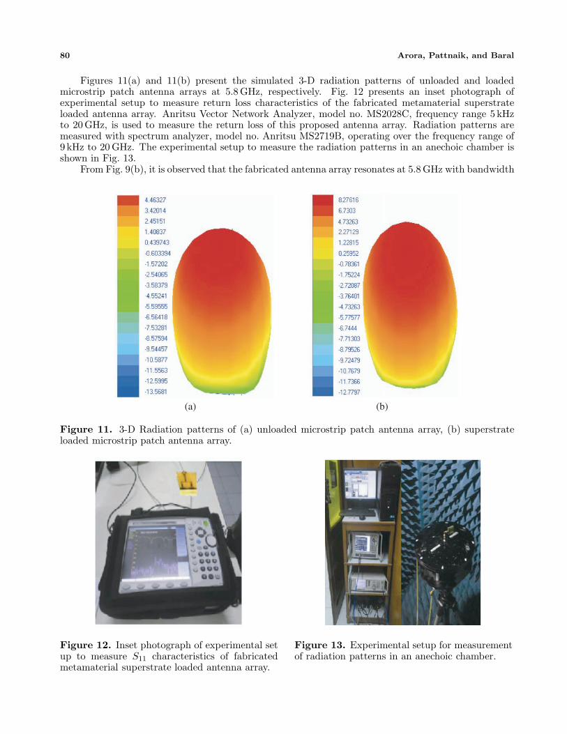
Figures 11(a) and 11(b) present the simulated 3-D radiation patterns of unloaded and loadedmicrostrip patch antenna arrays at 5.8 GHz, respectively. Fig. 12 presents an inset photograph ofexperimental setup to measure return loss characteristics of the fabricated metamaterial superstrateloaded antenna array. Anritsu Vector Network Analyzer, model no. MS2028C, frequency range 5 kHzto 20 GHz, is used to measure the return loss of this proposed antenna array. Radiation patterns aremeasured with spectrum analyzer, model no. Anritsu MS2719B, operating over the frequency range of9 kHz to 20 GHz. The experimental setup to measure the radiation patterns in an anechoic chamber isshown in Fig. 13.
From Fig. 9(b), it is observed that the fabricated antenna array resonates at 5.8 GHz with bandwidth
(a) (b)
Figure 11. 3-D Radiation patterns of (a) unloaded microstrip patch antenna array, (b) superstrateloaded microstrip patch antenna array.
Figure 12. Inset photograph of experimental setup to measure S11 characteristics of fabricatedmetamaterial superstrate loaded antenna array.
Figure 13. Experimental setup for measurementof radiation patterns in an anechoic chamber.

Progress In Electromagnetics Research B, Vol. 76, 2017 81
of about 600 MHz, showing that the two results are in good agreement with each other. However, somechange in the shapes of the two curves is due to the inaccuracy occurring while fabricating the proposedantenna array and the use of the FR-4 substrate, which is lossy in nature but quite cheap, and hence,suitable for making such prototypes.
3.2. Parametric Analysis
The height (d) between the proposed metamaterial superstrate and the ground plane of traditionalantenna array is an important parameter to decide the gain and bandwidth of the proposed array.To determine the optimized value of this height, so as to obtain the maximum improvement in gainand bandwidth of the proposed array, its parametric analysis is performed. Fig. 14 and Fig. 15 showthe variation of gain and VSWR at 5.8 GHz, respectively, of the proposed antenna array with thechange in d. It is observed that for d = 8 mm, maximum improvement in gain and VSWR is obtained.Occurrence of maximum improvement in the performance indices of the proposed antenna array, at thisparticular height, can be explained on the basis of increased coupling of metamaterial superstrate withthe traditional patch antenna array.
Figure 14. Variation in gain of proposed antennaarray as a function of height between superstratelayer and ground plane.
Figure 15. Variation in VSWR of proposedantenna array as a function of height betweensuperstrate layer and ground plane.
4. ANALYTICAL ANALYSIS AND EQUIVALENT CIRCUIT MODEL
Behavior mechanism and the equivalent circuit of the proposed metamaterial superstrate are discussedin this section. Various design equations of the equivalent circuit are also presented.
4.1. Analytical Analysis
Placing the proposed metamaterial superstrate over the patches of the antenna array at smallheight results in the parasitic loading of conventional patch antenna array. Due to this parasiticloading, proximity coupling between the superstrate and patch antenna occurs, thus forming a two-layer electromagnetically coupled system. This electromagnetic coupling between the patches andmetamaterial superstrate results in improvement of the bandwidth of the composite system. Gainenhancement of the proposed antenna array can be explained with the help of cavity effect, which

82 Arora, Pattnaik, and Baral
comes in existence when the superstrate layer forms the cover of the antenna patches. As per the Snell’sLaw of refraction, the medium with low refractive index moves the electromagnetic waves away fromthe primary source and in the direction parallel to the normal of this surface. This property resultsin directivity enhancement of the proposed antenna array. Moreover, at the resonant frequency, thecalculated reflection coefficient is approximately 0.79, showing that the metamaterial superstrate actsas a highly reflective surface, thus making the antenna highly directive. The presence of metamaterialsuperstrate also makes the field distribution of the patch antenna more uniform, thus improving theoverall gain of the proposed antenna array. Thus it is concluded that the metamaterial superstrate actsas a parasitic load that enhances the bandwidth, and the cavity effect improves the gain of the proposedantenna array.
4.2. Equivalent Circuit Model
Figure 16 shows the equivalent circuit of the microstrip patch antenna array loaded with a superstratelayer formed by split ring resonators. L and C represent the equivalent inductance and capacitance,respectively, of the split ring resonator, whereas L1 represents the equivalent inductance of microstrippatch. The resultant inductance of the port and feeding network is represented by Lf .
Figure 16. Equivalent circuit of proposed antenna array.
As per the principle of equivalent circuit theory, the modeling of split ring resonator can be doneas a LC resonant circuit, such that the values of equivalent inductance of SRR (L) and equivalentcapacitance of SRR (C) are calculated using Equations (5) and (6) [27].
L =μ0
2Lsavg
44.86
[ln
0.98ρ
+ 1.84ρ]
(5)

Progress In Electromagnetics Research B, Vol. 76, 2017 83
where, μ0 is the permeability of free space, ρ the filling ratio, Lsavg the average length of the squareSRR, which is given as Lsavg = 4[Ls− (N −1)(w + s)], and N the number of split rings. The equivalentcapacitance (C) of SRR is given as [27]
C = ε0N − 1
2
[2Ls − (2N − 1) (w + s)
K√
1 − k21
K (k1)
](6)
where, ε0 is the permittivity of free space, K the complete elliptic integral of first kind, and k1 theargument of integral expressed as (s/2)/(w + s/2).
When the metamaterial superstrate is placed close to the patch, the SRRs get inductively coupledwith the patch antenna because there exists some mutual inductance (M1 and M2) between them. Thismutual inductance between SRRs and the patch antenna is calculated using Equation (7), and its valueis 1.11 nH.
M1 = M2 =μ0Ls
2π
[0.467 +
0.059(w + W )2
L2s
](7)
There also exists some mutual inductance between the neighboring SRRs (M3) and neighboringpatches (M4), whose magnitudes are calculated using Equations (8) and (9) [28], and are found to be0.943 nH and 1.589 nH, respectively.
M3 =μ0Ls
2π
[0.467 +
0.059(w)2
L2s
](8)
M4 = −μL
2π
[ln(1 +
√2) + 1 −
√2 + w2
√2/24L2
](9)
Due to the conducting nature of patches and split rings, they also possess some self inductance.The self inductance (Ms) of the rectangular patch antenna is given by Equation (10) [28].
Ms =μL
2π
[ln
(2Lw
)+ 0.5 +
w
3L− w2
24L2
](10)
The inductance of the microstrip patch antenna array, with the capacitance of SRRs and mutualinductances, makes the loaded antenna behave as LC resonant circuit. This capacitance compensatesthe inductance of the microstrip patch array, and thus, under loaded conditions, good matching isobtained at the resonant frequency.
5. CONCLUSIONS
A metamaterial superstrate loaded microstrip patch antenna array for IEEE 802.16a 5.8 GHz Wi-MAXapplications has been developed. The proposed composite structure enhances the gain of a conventionalpatch antenna array by 86% and improves the bandwidth by 60% while maintaining almost same profileand cost. The equivalent circuit of the proposed antenna array is designed and analyzed. The proposedantenna array is fabricated and tested to support the simulated results. The performance comparison ofthe conventional unloaded antenna array and proposed metamaterial superstrate loaded antenna arrayshows that the metamaterials have good potential to improve the performance of antennas.
REFERENCES
1. Islam, M. A. and N. C. Karmakar, “A 4× 4 dual polarized mm-wave ACMPA array for a universalmm-wave chipless RFID tag reader,” IEEE Trans. Antennas Propag., Vol. 63, No. 4, 1633–1640,2015.
2. Kovitz, J. M. and Y. R. Samii, “Using thick substrates and capacitive probe compensation toenhance the bandwidth of traditional CP patch antennas,” IEEE Trans. Antennas Propag., Vol. 62,No. 8, 4970–4979, 2014.
3. Chow, Y. L. and K. L. Wan, “Miniaturizing patch antenna by adding a shorting pin near thefeed probe — A folded monopole equivalent,” Proc. of IEEE Antennas and Propagation SocietyInternational Symposium, 6–9, China, 2002.

84 Arora, Pattnaik, and Baral
4. Tang, X., H. Wong, Y. Long, Q. Xue, and K. L. Lau, “Circularly polarized shorted patch antennaon high permittivity substrate with wideband,” IEEE Trans. Antennas Propag., Vol. 60, No. 3,1588–1592, 2012.
5. Prasad, R. R., B. Srinu, and C. D. Raj, “Design and analysis of multi substrate microstrip patchantenna, microelectronics, electromagnetics and telecommunications,” Lecture Notes in ElectricalEngineering, Vol. 372, 733-739, Springer, India, 2016.
6. Mittra, R., Y. Li, and K. Yoo, “A comparative study of directivity enhancement of microstrippatch antennas with using three different superstrates,” Microw. Optical Technology Lett., Vol. 52,No. 2, 327–331, 2010.
7. Foroozesh, A. and L. Shafai, “Investigation into the effects of the patch type FSS superstrate onthe high-gain cavity resonance antenna design,” IEEE Trans. Antennas Propag., Vol. 58, No. 2,258–270, 2010.
8. Rao, N. and K. V. Dinesh, “Gain and bandwidth enhancement of a microstrip antenna using partialsubstrate removal in multiple-layer dielectric substrate,” Proc. of Progress In ElectromagneticsResearch Symposium, PIERS Proceedings, 1285–1289, Suzhou, China, September 12–16, 2011.
9. Attia, H. and O. M. Ramahi, “EBG superstrate for gain and bandwidth enhancement of microstriparray antennas,” Proc. of IEEE International Symposium on Antennas and Propagation AP-S 2008,1–4, Canada, 2008.
10. Nishiyama, E., M. Aikawa, and S. Egashira, “Stacked microstrip antenna for wideband and highgain,” IEE Proc. Microw. Antennas Propag., Vol. 151, No. 2, 143–148, 2004.
11. Honari, M. M., A. Abdipour, and G. Moradi, “Bandwidth and gain enhancement of an apertureantenna with modified ring patch,” IEEE Antennas Wirel. Propag. Lett., Vol. 10, 1413–1416, 2011.
12. Lapine, M. and S. Tretyakov, “Contemporary notes on metamaterials,” IET Microw., Antennasand Propag., Vol. 1, No. 1, 3–11, 2007.
13. Smith, D. R., W. J. Padilla, D. C. Vier, S. C. N. Nasser, and S. Schultz, “Composite mediumwith simultaneous negative permeability and permittivity,” Physical Review Lett., Vol. 84, No. 18,4184–4187, 2000.
14. Engheta, N. and R. W. Ziolkowski, “A positive future for double negative metamaterials,” IEEETrans. Microw. Theory Tech., Vol. 53, No. 4, 1535–1556, 2005.
15. Alu, A., N. Engheta, A. Erentok, and R. W. Ziolkowski, “Single negative, double-negative, andlow-index metamaterials and their electromagnetic applications,” IEEE Antennas and Propag.Magazine, Vol. 49, No. 1, 23–36, 2007.
16. Joshi, J. G., S. S. Pattnaik, and S. Devi, “Metamaterial embedded wearable rectangular microstrippatch antenna,” Hindawi Int. J. of Antennas and Propag., Vol. 2012, 1–9, 2012.
17. Joshi, J. G., S. S. Pattnaik, and S. Devi, “Metamaterial loaded square slotted dual band microstrippatch antenna,” Proc. of IEEE Applied Electromagnetics Conference (AEMC-2011), 1–4, India,2011.
18. Ferdous, S., A. Hossain, S. M. H. Chowdhury, and M. R. C. Mahdy, “Reduced and conventional sizemulti-band circular patch antennas loaded with metamaterials,” IET J. Micro., Antennas Propag.,Vol. 7, No. 7, 768–776, 2013.
19. Chaimool, S., K. L. Chung, and P. Akkaraekthalin, “Simultaneous gain and bandwidthsenhancement of a single-feed circularly polarized microstrip patch antenna using a metamaterialreflective surface,” Progress In Electromagnetics Research B, Vol. 22, 23–37, 2010.
20. Chung, K. L. and S. Chaimool, “Broadside gain and bandwidth enhancement of microstrip patchantenna using a MNZ-metasurface,” Microw. Optical Technology Lett., Vol. 54, No. 2, 529–532,2012.
21. Arora, C., S. S. Pattnaik, and R. N. Baral, “SRR inspired microstrip patch antenna array,” ProgressIn Electromagnetics Research C, Vol. 58, No. 8, 89–96, 2015.
22. Arora, C., S. S. Pattnaik, and R. N. Baral, “Microstrip patch antenna array with metamaterialground plane for Wi-MAX applications,” Proc. of the Springer Second International Conferenceon Computer and Communication Technologies (IC3T-2015), 665–672, India, 2015.

Progress In Electromagnetics Research B, Vol. 76, 2017 85
23. Arora, C., S. S. Pattnaik, and R. N. Baral, “Metamaterial superstrate for performance enhancementof microstrip patch antenna array,” 3rd International Conference on Signal Processing andIntegrated Networks (SPIN-2016), 775–779, India, 2016.
24. Garg, R., P. Bhartia, I. Bhal, and A. Ittipiboon, Microstrip Antenna Design Handbook, ArtechHouse, Boston, UK, 2001.
25. Balanis, C. A., Modern Antenna Handbook, John Wiley & Sons, New York, USA, 2011.26. Pozar, D. M., Microwave Engineering, John Wiley & Sons, New York, USA, 2008.27. Joshi, J. G., S. S. Pattnaik, S. Devi, and M. R. Lohokare, “Frequency switching of electrically small
patch antenna using metamaterial loading,” Indian J. Radio Sp. Phys., Vol. 40, No. 3, 159–165,2011.
28. Joshi, J. G., S. S. Pattnaik, and S. Devi, “Geo-textile based metamaterial loaded wearablemicrostrip patch antenna,” International J. Microw. Optical Technology, Vol. 8, No. 1, 25–33,2013.