Sri Satya Sai University of Technology & Medical Sciences
19
Sri Satya Sai University of Technology & Medical Sciences Digital electronics Notes Introducation Digital electronics are systems that represent signals as discrete levels, rather than as a continuous range. In most cases the number of states is two, and these states are represented by two voltage levels: one near to zero volts and one at a higher level depending on the supply voltage in use. These two levels are often represented as "Low" and "High". The fundamental advantage of digital techniques stem from the fact it is easier to get an electronic device to switch into one of a number of known states than to accurately reproduce a continuous range of values. Digital electronics are usually made from large assemblies of logic gates, simple electronic representations of Boolean logic functions. This chapter is an introduction to Digital Logic circutes. Logic gate A logic gate performs a logical operation on one or more logic inputs and produces a single logic output. Because the output is also a logic-level value, an output of one logic gate can connect to the input of one or more other logic gates. The logic normally performed is Boolean logic and is most commonly found in digital circuits. Logic gates are primarily implemented electronically using diodes or transistors, but can also be constructed using electromagnetic relays, fluidics, optics, molecules, or even mechanical elements. In electronic logic, a logic level is represented by a voltage or current, (which depends on the type of electronic logic in use). Each logic gate requires power so that it can source and sink currents to achieve the correct output voltage. In logic circuit diagrams the power is not shown, but in a full electronic schematic, power connections are required. Binary information is represented in digital computer by physical quantities called signals. Electrical signal such as voltages exist throughout the computer in either one of two recognizable states. The two states represent a binary variable that can be equal to 1 or 0. Binary logic deal with binary variables and with operations that assume a logical meaning. It is used to describe, in algebric or tabular form, the manipulation and processing of binary information. The manipulation of bianary information is done by logic circuits called gates. Gates are blocks of hardware that produce signal of binary 1 or 0 when input logic requirements are satisfied. Logic gates process signals which represent true or false. Normally the positive supply voltage +Vs represents true and 0V represents false. Other terms which are used for the true and false states are shown in the table:
Transcript of Sri Satya Sai University of Technology & Medical Sciences

Sri Satya Sai University of Technology & Medical Sciences
Digital electronics Notes
Introducation
Digital electronics are systems that represent signals as discrete levels, rather than as a
continuous range. In most cases the number of states is two, and these states are represented
by two voltage levels: one near to zero volts and one at a higher level depending on the supply
voltage in use. These two levels are often represented as "Low" and "High".
The fundamental advantage of digital techniques stem from the fact it is easier to get an
electronic device to switch into one of a number of known states than to accurately reproduce a
continuous range of values.
Digital electronics are usually made from large assemblies of logic gates, simple electronic
representations of Boolean logic functions. This chapter is an introduction to Digital Logic
circutes.
Logic gate
A logic gate performs a logical operation on one or more logic inputs and produces a single logic
output. Because the output is also a logic-level value, an output of one logic gate can connect
to the input of one or more other logic gates. The logic normally performed is Boolean logic and
is most commonly found in digital circuits. Logic gates are primarily implemented electronically
using diodes or transistors, but can also be constructed using electromagnetic relays, fluidics,
optics, molecules, or even mechanical elements.
In electronic logic, a logic level is represented by a voltage or current, (which depends on the
type of electronic logic in use). Each logic gate requires power so that it can source and sink
currents to achieve the correct output voltage. In logic circuit diagrams the power is not shown,
but in a full electronic schematic, power connections are required.
Binary information is represented in digital computer by physical quantities called signals.
Electrical signal such as voltages exist throughout the computer in either one of two
recognizable states. The two states represent a binary variable that can be equal to 1 or 0.
Binary logic deal with binary variables and with operations that assume a logical meaning. It is
used to describe, in algebric or tabular form, the manipulation and processing of binary
information. The manipulation of bianary information is done by logic circuits called gates. Gates
are blocks of hardware that produce signal of binary 1 or 0 when input logic requirements are
satisfied.
Logic gates process signals which represent true or false. Normally the positive supply
voltage +Vs represents true and 0V represents false. Other terms which are used for the true
and false states are shown in the table:

Sri Satya Sai University of Technology & Medical Sciences
Logic states
TRUE FALSE
0 1
HIGH LOW
+Vs 0V
On Off
Type Of Gates:
NOT Gates
AND Gates
OR Gates
NAND Gate
NOR Gate
NOT Gates:
In digital logic, an inverter or NOT gate is a logic gate which implements logical negation.The
NOT gate is an electronic circuit that produces an inverted version of the input at its output. It
is also known as an inverter. If the input variable is A, the inverted output is known as NOT A.
This is also shown as A', or A with a bar over the top, as shown at the outputs. The diagrams
below show two ways that the NAND logic gate can be configured to produce a NOT gate. It can
also be done using NOR logic gates in the same way.
There are symbol for AND gates:
Truth Table:
Input Output
A A'
0 1
1 0
AND Gates:
The AND gate is a digital logic gate that implements logical conjunction - it behaves according
to the truth table to the right. A HIGH output (1) results only if both the inputs to the AND

Sri Satya Sai University of Technology & Medical Sciences
gate are HIGH (1). If neither or only one input to the AND gate is HIGH, a LOW output results.
In another sense, the function of AND effectively finds the minimum between two binary digits,
just as the OR function finds the maximum.
There are symbol for AND gates:
The AND gate with inputs A and B and output C implements the logical expression
C=A.B
Truth Table:
Input Output
A B C=A.B
0 0 0
0 1 0
1 0 0
1 1 1
OR Gates:
The OR gate is a digital logic gate that implements logical disjunction - it behaves according to
the truth table to the right. A HIGH output (1) results if one or both the inputs to the gate are
HIGH (1). If neither input is HIGH, a LOW output (0) results. In another sense, the function of
OR effectively finds the maximum between two binary digits, just as the complementary AND
function finds the minimum.
There are symbol for OR gates:
The OR gate with inputs A and B and output C implements the logical expression
C=A+B
Truth Table:

Sri Satya Sai University of Technology & Medical Sciences
Input Output
A B C=A+B
0 0 0
0 1 1
1 0 1
1 1 1
NAND gates (NAND = Not AND)
The NAND gate is a digital logic gate that behaves in a manner that corresponds to the
truth table to the left. A LOW output results only if both the inputs to the gate are HIGH. If
one or both inputs are LOW, a HIGH output results. The NAND gate is a universal gate in the
sense that any boolean function can be implemented by NAND gates.
Digital systems employing certain logic circuits take advantage of NAND's functional
completeness. In complicated logical expressions, normally written in terms of other logic
functions such as AND, OR, and NOT, writing these in terms of NAND saves on cost, because
implementing such circuits using NAND gate yields a more compact result than the alternatives.
NAND gates can also be made with more than two inputs, yielding an output of LOW if all
of the inputs are HIGH, and an output of HIGH if any of the inputs is LOW. These kinds of
gates therefore operate as n-ary operators instead of a simple binary operator. Algebraically,
these can be expressed as the function NAND(a,b,......n), which is logically equivalent to NOT(a
AND b AND ... AND n).
There are symbol for NAND gates:
Truth Table:
Input Output
A B C=A NAND B
0 0 1
0 1 1
1 0 1
1 1 0

Sri Satya Sai University of Technology & Medical Sciences
NOR gates (NOR = Not OR):
The NOR gate is a digital logic gate that implements logical NOR - it behaves according
to the truth table to the right. A HIGH output (1) results if both the inputs to the gate are LOW
(0). If one or both input is HIGH (1), a LOW output (0) results. NOR is the result of the
negation of the OR operator. NOR is a functionally complete operation—combinations of NOR
gates can be combined to generate any other logical function. By contrast, the OR operator is
monotonic as it can only change LOW to HIGH but not vice versa.
In most, but not all, circuit implementations, the negation comes for free—including
CMOS and TTL. In such logic families, the only way to implement OR is with 2 or more gates,
such as a NOR followed by an inverter. A significant exception is some forms of the domino logic
family.
There are symbol for NOR gates:
Truth Table:
Input Output
A B C=A NOR B
0 0 1
0 1 0
1 0 0
1 1 0
The NAND and NOR gates are called universal functions since with either one the AND
and OR functions and NOT can be generated.
XOR gates (Exclusive OR)
The XOR gate (sometimes EOR gate) is a digital logic gate that implements exclusive
disjunction - it behaves according to the truth table above. A HIGH output (1) results if one,
and only one, of the inputs to the gate is HIGH (1). If both inputs are LOW (0) or both are
HIGH (1), a LOW output (0) results.
XOR gate is short for exclusive OR. This means that precisely one input must be 1 (true)
for the output to be 1 (true). A way to remember XOR is "one or the other but not both."
This function is addition modulo 2. As a result, XOR gates are used to implement binary
addition in computers. A half adder consists of an XOR gate and an AND gate.
There are symbol for XOR gates:

Sri Satya Sai University of Technology & Medical Sciences
The XOR gate with inputs A and B implements the logical expression A.B`+A`.B .
Truth Table:
Input Output
A B C=A XOR B
0 0 0
0 1 1
1 0 1
1 1 0
XNOR gates (Exclusive NOR)
The XNOR gate (sometimes spelled "exnor" or "enor") is a digital logic gate whose
function is the inverse of the exclusive OR (XOR) gate. The two-input version implements
logical equality, behaving according to the truth table to the right. A HIGH output (1) results if
both of the inputs to the gate are the same. If one but not both inputs are HIGH (1), a LOW
output (0) results.
There are symbol for XNOR gates:
Truth Table:
Input Output
A B C=A XOR B
0 0 1
0 1 0
1 0 0
1 1 1

Sri Satya Sai University of Technology & Medical Sciences
C
o
m
b
i
n
a
t
i
o
n
s
o
f
l
o
g
i
c
g
a
tes
Logic gates can be combined to produce more complex functions. They can also be
combined to substitute one type of gate for another.
For example to produce an output Q which is true only when
input A is true and input B is false, as shown in the truth table on
the right, we can combine a NOT gate and an AND gate like this:
Q = A AND NOT B
Input A Input B Output Q
0 0 0
0 1 0
1 0 1
1 1 0
Sri Satya Sai University of Technology & Medical Sciences
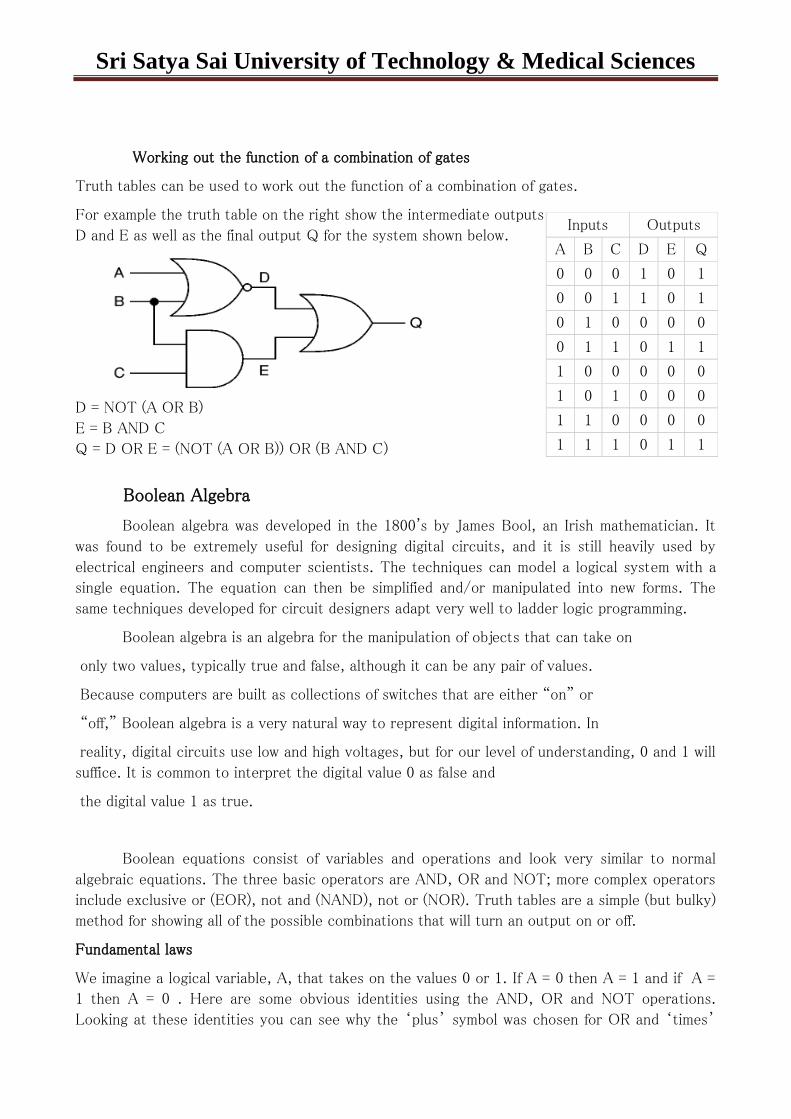
Working out the function of a combination of gates
Truth tables can be used to work out the function of a combination of gates.
For example the truth table on the right show the intermediate outputs
D and E as well as the final output Q for the system shown below.
D = NOT (A OR B)
E = B AND C
Q = D OR E = (NOT (A OR B)) OR (B AND C)
Boolean Algebra
Boolean algebra was developed in the 1800's by James Bool, an Irish mathematician. It
was found to be extremely useful for designing digital circuits, and it is still heavily used by
electrical engineers and computer scientists. The techniques can model a logical system with a
single equation. The equation can then be simplified and/or manipulated into new forms. The
same techniques developed for circuit designers adapt very well to ladder logic programming.
Boolean algebra is an algebra for the manipulation of objects that can take on
only two values, typically true and false, although it can be any pair of values.
Because computers are built as collections of switches that are either “on” or
“off,” Boolean algebra is a very natural way to represent digital information. In
reality, digital circuits use low and high voltages, but for our level of understanding, 0 and 1 will
suffice. It is common to interpret the digital value 0 as false and
the digital value 1 as true.
Boolean equations consist of variables and operations and look very similar to normal
algebraic equations. The three basic operators are AND, OR and NOT; more complex operators
include exclusive or (EOR), not and (NAND), not or (NOR). Truth tables are a simple (but bulky)
method for showing all of the possible combinations that will turn an output on or off.
Fundamental laws
We imagine a logical variable, A, that takes on the values 0 or 1. If A = 0 then A = 1 and if A =
1 then A = 0 . Here are some obvious identities using the AND, OR and NOT operations.
Looking at these identities you can see why the ‘plus’ symbol was chosen for OR and ‘times’
Inputs Outputs
A B C D E Q
0 0 0 1 0 1
0 0 1 1 0 1
0 1 0 0 0 0
0 1 1 0 1 1
1 0 0 0 0 0
1 0 1 0 0 0
1 1 0 0 0 0
1 1 1 0 1 1

Sri Satya Sai University of Technology & Medical Sciences
was chosen for AND.
OR
A+0= A
A +1 = 1
A+ A= A
A + A =1
AND
A• 0 = 0
A•1 = A
A• A = A
A• A = 0
NOT
A + A =1
A• A = 0
A=A
Two Boolean expressions are equal if and only if their truth tables are identical.
The Basic Axioms of Boolean Algebra
DeMorgan's Theorems
A mathematician named DeMorgan developed a pair of important rules regarding group
complementation in Boolean algebra. By group complementation, I'm referring to the
complement of a group of terms, represented by a long bar over more than one variable.
You should recall from the chapter on logic gates that inverting all inputs to a gate

Sri Satya Sai University of Technology & Medical Sciences
reverses that gate's essential function from AND to OR, or visa-versa, and also inverts the
output. So, an OR gate with all inputs inverted (a Negative-OR gate) behaves the same as a
NAND gate, and an AND gate with all inputs inverted (a Negative-AND gate) behaves the same
as a NOR gate. DeMorgan's theorems state the same equivalence in "backward" form: that
inverting the output of any gate results in the same function as the opposite type of gate (AND
vs. OR) with inverted inputs:
A long bar extending over the term AB acts as a grouping symbol, and as such is entirely
different from the product of A and B independently inverted. In other words, (AB)' is not equal
to A'B'. Because the "prime" symbol (') cannot be stretched over two variables like a bar can,
we are forced to use parentheses to make it apply to the whole term AB in the previous
sentence. A bar, however, acts as its own grouping symbol when stretched over more than one
variable. This has profound impact on how Boolean expressions are evaluated and reduced, as we
shall see.
DeMorgan's theorem may be thought of in terms of breaking a long bar symbol. When a long bar
is broken, the operation directly underneath the break changes from addition to multiplication,
or visa-versa, and the broken bar pieces remain over the individual variables. To illustrate:

Sri Satya Sai University of Technology & Medical Sciences
Example of Proof
Each of the above equalities is a theorem that can be proved. Let’s do an example by directly
comparing the truth tables for the left and right sides. We take on DeMorgan’s first theorem for
two variables, A and B.
Truth Table:
(A.B)'
A B A.B (A.B)'
0 0 0 1
0 1 0 1
1 0 0 1
1 1 1 0
(A'+B')
A B A' B' A'+B'
0 0 1 1 1
0 1 1 0 1
1 0 0 1 1
1 1 0 0 0
The last columns of the truth tables are identical. Thus, the first theorem is proven for two
variables.
Simplification of Boolean Expressions
The algebraic identities we studied in algebra class allow us to reduce algebraic
expressions (such as 10x + 2y - x + 3y) to their simplest forms (9x + 5y). The
Boolean identities can be used to simplify Boolean expressions in a similar fashion. We apply
these identities in the following examples.
EXAMPLE:
Suppose we have the function F(x,y) = xy + xy. Using the OR form of the Idempotent Law and
treating the expression xy as a Boolean variable,
We simplify the original expression to xy. Therefore, F(x,y) = xy + xy = xy.
Karnaugh map
A Karnaugh map (K-map) is a pictorial method used to minimize Boolean expressions without
having to use Boolean algebra theorems and equation manipulations. A K-map can be thought of
as a special version of a truth table .

Sri Satya Sai University of Technology & Medical Sciences
Using a K-map, expressions with two to four variables are easily minimized. Expressions with
five to six variables are more difficult but achievable, and expressions with seven or more
variables are extremely difficult (if not impossible) to minimize using a K-map.
Why learn about Karnaugh maps? The Karnaugh map, like Boolean algebra, is a simplification
tool applicable to digital logic.The Karnaugh Map will simplify logic faster and more easily in
most cases.
Boolean simplification is actually faster than the Karnaugh map for a task involving two or fewer
Boolean variables. It is still quite usable at three variables, but a bit slower. At four input
variables, Boolean algebra becomes tedious. Karnaugh maps are both faster and easier.
Karnaugh maps work well for up to six input variables, are usable for up to eight variables. For
more than six to eight variables, simplification should be by CAD (computer automated design).
Recommended logic simplification vs number of Inputs
Variable Boolean Algebra Karnaugh Map Computer automated
1--2 X ?
3 X X ?
4 ? X ?
5--6 X X
7—8 ? X
>8 X
In theory any of the three methods will work. However, as a practical matter, the above
guidelines work well. We would not normally resort to computer automation to simplify a three
input logic block. We could sooner solve the problem with pencil and paper. However, if we had
seven of these problems to solve, say for a BCD (Binary Coded Decimal) to seven segment decoder, we might want to automate the process. A BCD to seven segment decoder generates
the logic signals to drive a seven segment LED (light emitting diode) display.
Examples of computer automated design languages for simplification of logic are PALASM,
ABEL, CUPL, Verilog, and VHDL. These programs accept a hardware descriptor language input
file which is based on Boolean equations and produce an output file describing a reduced (or
simplified) Boolean solution.
Making a Venn diagram look like a Karnaugh map
Starting with circle A in a rectangular A' universe in figure (a) below, we morph a Venn diagram
into almost a Karnaugh map.

Sri Satya Sai University of Technology & Medical Sciences
We
expand
circle
A at (b)
and (c),
confor
m to
the
rectang
ular A'
universe at (d), and change A to a rectangle at (e). Anything left outside of A is A' . We assign a
rectangle to A' at (f). Also, we do not use shading in Karnaugh maps. What we have so far
resembles a 1-variable Karnaugh map, but is of little utility. We need multiple variables.
Figure
(a)
above
is the
same
as the
previou
s Venn
diagram
showing A and A' above except that the labels A and A' are above the diagram instead of inside
the respective regions. Imagine that we have go through a process similar to figures (a-f) to get
a "square Venn diagram" for B and B' as we show in middle figure (b). We will now superimpose
the diagrams in Figures (a) and (b) to get the result at (c), just like we have been doing for Venn
diagrams. The reason we do this is so that we may observe that which may be common to two
overlapping regions-- say where A overlaps B. The lower right cell in figure (c) corresponds to
AB where A overlaps B.
We don't waste time drawing a Karnaugh map like (c) above, sketching a simplified version as
above left instead. The column of two cells under A' is understood to be associated with A', and
the heading A is associated with the column of cells under it. The row headed by B' is associated
with the cells to the right of it. In a similar manner B is associated with the cells to the right of
it. For the sake of simplicity, we do not delineate the various regions as clearly as with Venn
diagrams.

Sri Satya Sai University of Technology & Medical Sciences
The Karnaugh map above right is an alternate form used in most texts. The names of the
variables are listed next to the diagonal line. The A above the diagonal indicates that the
variable A (and A') is assigned to the columns. The 0 is a substitute for A', and the 1 substitutes
for A. The B below the diagonal is associated with the rows: 0 for B', and 1 for B
Example:
Mark the cell corresponding to the Boolean expression AB in the Karnaugh map above with a 1
Solution:
Shade or circle the region corresponding to A. Then, shade or enclose the region
corresponding to B. The overlap of the two regions is AB. Place a 1 in this cell. We do not
necessarily enclose the A and B regions as at above left.
We
develop
a 3-
variabl
e
Karnau
gh map
above,
starting
with
Venn
diagram
like
regions
. The universe (inside the black rectangle) is split into two narrow narrow rectangular regions for
A' and A. The variables B' and B divide the universe into two square regions. C occupies a
square region in the middle of the rectangle, with C' split into two vertical rectangles on each
side of the C square.
In the final figure, we superimpose all three variables, attempting to clearly label the various
regions. The regions are less obvious without color printing, more obvious when compared to the
other three figures. This 3-variable K-Map (Karnaugh map) has 23 = 8 cells, the small squares
within the map. Each individual cell is uniquely identified by the three Boolean Variables (A, B,
C). For example, ABC' uniquely selects the lower right most cell(*), A'B'C' selects the upper
left most cell (x).

Sri Satya Sai University of Technology & Medical Sciences
We
don't
normall
y label
the
Karnau
gh map
as
shown above left. Though this figure clearly shows map coverage by single boolean variables of a
4-cell region. Karnaugh maps are labeled like the illustration at right. Each cell is still uniquely
identified by a 3-variable product term, a Boolean AND expression. Take, for example, ABC'
following the A row across to the right and the BC' column down, both intersecting at the lower
right cell ABC'.
See (*) above
figure.
The above two different forms of a 3-variable Karnaugh map are equivalent, and is the final form
that it takes. The version at right is a bit easier to use, since we do not have to write down so
many boolean alphabetic headers and complement bars, just 1s and 0s Use the form of map on
the right and look for the the one at left in some texts. The column headers on the left B'C',
B'C, BC, BC' are equivalent to 00, 01, 11, 10 on the right. The row headers A, A' are
equivalent to 0, 1 on the right map.
Karnaugh maps, truth tables
The Output of the Boolean equation may be computed by the laws of Boolean algebra and
transfered to the truth table or Karnaugh map.
The outputs of a truth table correspond on a one-to-one basis to Karnaugh map entries.
Starting at the top of the truth table, the A=0, B=0 inputs produce an output α. Note that this

Sri Satya Sai University of Technology & Medical Sciences
same output α is found in the Karnaugh map at the A=0, B=0 cell address, upper left corner of
K-map where the A=0 row and B=0 column intersect. The other truth table outputs β, χ, δ
from inputs AB=01, 10, 11 are found at corresponding K-map locations.
Below, we show the adjacent 2-cell regions in the 2-variable K-map with the aid of previous
rectangular Venn diagram like Boolean regions.
Cells α and χ are adjacent in the K-map as ellipses in the left most K-map below. Referring to
the previous truth table, this is not the case. There is another truth table entry (β) between
them. Which brings us to the whole point of the organizing the K-map into a square array, cells
with any Boolean variables in common need to be close to one another so as to present a pattern
that jumps out at us. For cells α and χ they have the Boolean variable B' in common. We
know this because B=0 (same as B') for the column above cells α and χ. Compare this to the
square Venn diagram above the K-map.
A similar line of reasoning shows that β and δ have Boolean B (B=1) in common. Then, α and
β have Boolean A' (A=0) in common. Finally, χ and δ have Boolean A (A=1) in common.
Compare the last two maps to the middle square Venn diagram.
To summarize, we are looking for commonality of Boolean variables among cells. The Karnaugh
map is organized so that we may see that commonality. Let's try some examples.

Sri Satya Sai University of Technology & Medical Sciences
Example:
Transfer the contents of the truth table to the Karnaugh map above.
Solution:
The truth table contains two 1s. the K- map must have both of them. locate the first 1 in the
2nd row of the truth table above.
note the truth table AB address
locate the cell in the K-map having the same address
place a 1 in that cell
Repeat the process for the 1 in the last line of the truth table.
Example:
For the Karnaugh map in the above problem, write the Boolean expression. Solution is below.
Solution:
Look for adjacent cells, that is, above or to the side of a cell. Diagonal cells are not adjacent.
Adjacent cells will have one or more Boolean variables in common.
Group (circle) the two 1s in the column

Sri Satya Sai University of Technology & Medical Sciences
Find the variable(s) top and/or side which are the same for the group, Write this as the
Boolean result. It is B in our case.
Ignore variable(s) which are not the same for a cell group. In our case A varies, is both 1
and 0, ignore Boolean A.
Ignore any variable not associated with cells containing 1s. B' has no ones under it.
Ignore B'
Result Out = B
This might be easier to see by comparing to the Venn diagrams to the right, specifically the B
column.
Example:
For the Truth table below, transfer the outputs to the Karnaugh, then write the Boolean
expression for the result.
Solution:
Transfer the 1s from the locations in the Truth table to the corresponding locations in the K-
map.
Group (circle) the two 1's in the column under B=1
Group (circle) the two 1's in the row right of A=1
Write product term for first group = B
Write product term for second group = A
Write Sum-Of-Products of above two terms Output = A+B
The solution of the K-map in the middle is the simplest or lowest cost solution. A less desirable
solution is at far right. After grouping the two 1s, we make the mistake of forming a group of 1-
cell. The reason that this is not desirable is that:
The single cell has a product term of AB'
The corresponding solution is Output = AB' + B
This is not the simplest solution
The way to pick up this single 1 is to form a group of two with the 1 to the right of it as shown in
the lower line of the middle K-map, even though this 1 has already been included in the column
group (B). We are allowed to re-use cells in order to form larger groups. In fact, it is desirable
because it leads to a simpler result.
We need to point out that either of the above solutions, Output or Wrong Output, are logically

Sri Satya Sai University of Technology & Medical Sciences
correct. Both circuits yield the same output. It is a matter of the former circuit being the lowest
cost solution.
Example:
Simplify the logic diagram below.
Solution: (Figure below)
Write the Boolean expression for the original logic diagram as shown below
Transfer the product terms to the Karnaugh map
Form groups of cells as in previous examples
Write Boolean expression for groups as in previous examples
Draw simplified logic diagram
Logic simplification with Karnaugh maps