
Spintronic Technology & Advance Research (STAR) Department ...

Spin dynamics in hybrid spintronic devices andsemiconductor nanostructuresRietjens, J.H.H.
DOI:10.6100/IR640282
Published: 01/01/2009
Document VersionPublisher’s PDF, also known as Version of Record (includes final page, issue and volume numbers)
Please check the document version of this publication:
• A submitted manuscript is the author's version of the article upon submission and before peer-review. There can be important differencesbetween the submitted version and the official published version of record. People interested in the research are advised to contact theauthor for the final version of the publication, or visit the DOI to the publisher's website.• The final author version and the galley proof are versions of the publication after peer review.• The final published version features the final layout of the paper including the volume, issue and page numbers.
Link to publication
General rightsCopyright and moral rights for the publications made accessible in the public portal are retained by the authors and/or other copyright ownersand it is a condition of accessing publications that users recognise and abide by the legal requirements associated with these rights.
• Users may download and print one copy of any publication from the public portal for the purpose of private study or research. • You may not further distribute the material or use it for any profit-making activity or commercial gain • You may freely distribute the URL identifying the publication in the public portal ?
Take down policyIf you believe that this document breaches copyright please contact us providing details, and we will remove access to the work immediatelyand investigate your claim.
Download date: 15. Jul. 2018

Spin dynamics in hybrid spintronic devices andsemiconductor nanostructures
PROEFSCHRIFT
ter verkrijging van de graad van doctoraan de Technische Universiteit Eindhoven,
op gezag van de Rector Magnificus,prof.dr.ir. C.J. van Duijn,
voor een commissie aangewezen door het College voor Promotiesin het openbaar te verdedigen
op maandag 9 februari 2009 om 16.00 uur
door
Jeroen Henricus Hubertus Rietjens
geboren te Weert
Dit proefschrift is goedgekeurd door de promotoren:
prof.dr. B. Koopmansenprof.dr.ir. H.J.M. Swagten
Copromotor:dr. E.P.A.M. Bakkers
A catalogue record is available from the Eindhoven University of Technology Library
ISBN: 978-90-386-1525-7
The work described in this Thesis has been carried out in the group Physics ofNanostructures, at the Department of Applied Physics of the Eindhoven Universityof Technology, the Netherlands.
This research was supported by NanoNed, a national nanotechnology program co-ordinated by the Dutch Ministry of Economic Affairs. Flagship NanoSpintronics.Project number 7160 / 6473 - 2C1.
Printed by Universiteitsdrukkerij Technische Universiteit Eindhoven
Cover design by Jeroen Rietjens and Frans Snik

Dedicated to:
Huub,
Femke
en
Guus

iv
Contents
1 Introduction 11.1 Spintronics . . . . . . . . . . . . . . . . . . . . . . . . . . . . . . . . 11.2 Semiconductor Spintronics . . . . . . . . . . . . . . . . . . . . . . . . 31.3 This Thesis . . . . . . . . . . . . . . . . . . . . . . . . . . . . . . . . 6
2 Magnetization and spin dynamics 132.1 Magnetization dynamics in ferromagnets . . . . . . . . . . . . . . . . 142.2 Optical orientation in semiconductors . . . . . . . . . . . . . . . . . 162.3 Spin relaxation mechanisms . . . . . . . . . . . . . . . . . . . . . . . 182.4 Modeling spin relaxation in n−GaAs . . . . . . . . . . . . . . . . . . 212.5 Spin precession and dephasing . . . . . . . . . . . . . . . . . . . . . . 27
3 Magneto-optical techniques 333.1 MOKE . . . . . . . . . . . . . . . . . . . . . . . . . . . . . . . . . . . 34
3.1.1 Basics of MOKE . . . . . . . . . . . . . . . . . . . . . . . . . 343.1.2 Measuring MOKE . . . . . . . . . . . . . . . . . . . . . . . . 363.1.3 An example: the AlOx / CoFeB / Pd system . . . . . . . . . 373.1.4 MOKE in a general multilayer system . . . . . . . . . . . . . 393.1.5 A case study: Co/Pt multilayers . . . . . . . . . . . . . . . . 42
3.2 TR-MOKE . . . . . . . . . . . . . . . . . . . . . . . . . . . . . . . . 453.3 TiMMS . . . . . . . . . . . . . . . . . . . . . . . . . . . . . . . . . . 48
3.3.1 TiMMS-setup . . . . . . . . . . . . . . . . . . . . . . . . . . . 483.3.2 Signal analysis . . . . . . . . . . . . . . . . . . . . . . . . . . 513.3.3 An example: TiMMS on a spin injection device . . . . . . . . 53
3.4 Modeling TiMMS for heterostructures . . . . . . . . . . . . . . . . . 59
4 MRAM element 694.1 Introduction . . . . . . . . . . . . . . . . . . . . . . . . . . . . . . . . 704.2 Experimental details . . . . . . . . . . . . . . . . . . . . . . . . . . . 70
4.2.1 The MTJ element . . . . . . . . . . . . . . . . . . . . . . . . 704.2.2 Measurement technique . . . . . . . . . . . . . . . . . . . . . 704.2.3 Micromagnetic simulations . . . . . . . . . . . . . . . . . . . 72
v
vi CONTENTS
4.3 Results and discussion . . . . . . . . . . . . . . . . . . . . . . . . . . 724.3.1 Domain imaging . . . . . . . . . . . . . . . . . . . . . . . . . 724.3.2 Local spin modes . . . . . . . . . . . . . . . . . . . . . . . . . 74
4.4 Conclusion . . . . . . . . . . . . . . . . . . . . . . . . . . . . . . . . 76
5 Spin-LED 795.1 Introduction . . . . . . . . . . . . . . . . . . . . . . . . . . . . . . . . 805.2 Experimental details . . . . . . . . . . . . . . . . . . . . . . . . . . . 80
5.2.1 Measurement technique . . . . . . . . . . . . . . . . . . . . . 805.2.2 The spin-LED . . . . . . . . . . . . . . . . . . . . . . . . . . 81
5.3 Results and Discussion . . . . . . . . . . . . . . . . . . . . . . . . . . 825.3.1 Current-induced enhancement of the spin relaxation rate . . 825.3.2 Other current induced effects . . . . . . . . . . . . . . . . . . 855.3.3 Spatially resolved measurements . . . . . . . . . . . . . . . . 90
5.4 Conclusion . . . . . . . . . . . . . . . . . . . . . . . . . . . . . . . . 915.5 Appendix . . . . . . . . . . . . . . . . . . . . . . . . . . . . . . . . . 92
5.5.1 Spectral measurements . . . . . . . . . . . . . . . . . . . . . . 925.5.2 Spatially resolved data . . . . . . . . . . . . . . . . . . . . . . 955.5.3 Current-voltage characteristic of the spin-LED . . . . . . . . 95
6 Nanowires 996.1 Introduction . . . . . . . . . . . . . . . . . . . . . . . . . . . . . . . . 1006.2 Experimental details . . . . . . . . . . . . . . . . . . . . . . . . . . . 1006.3 Probing ensembles of multi-segmented GaP / GaAs nanowires . . . . 101
6.3.1 Transient reflectivity measurements . . . . . . . . . . . . . . 1016.3.2 Magneto-optical measurements . . . . . . . . . . . . . . . . . 105
6.4 Probing single capped GaP / GaAs / GaP nanowires . . . . . . . . . 1066.4.1 Transient reflectivity measurements . . . . . . . . . . . . . . 1076.4.2 Magneto-optical measurements . . . . . . . . . . . . . . . . . 108
6.5 Conclusion . . . . . . . . . . . . . . . . . . . . . . . . . . . . . . . . 112
7 Quantum dots 1157.1 Introduction . . . . . . . . . . . . . . . . . . . . . . . . . . . . . . . . 1167.2 Experimental details . . . . . . . . . . . . . . . . . . . . . . . . . . . 116
7.2.1 Quantum dot growth and properties . . . . . . . . . . . . . . 1167.2.2 Measurement technique: TiMMS . . . . . . . . . . . . . . . . 117
7.3 Results and discussion . . . . . . . . . . . . . . . . . . . . . . . . . . 1187.3.1 Spin capture, precession and relaxation . . . . . . . . . . . . 1187.3.2 Electric field dependence . . . . . . . . . . . . . . . . . . . . . 121
7.4 Conclusion . . . . . . . . . . . . . . . . . . . . . . . . . . . . . . . . 121
Summary 125

CONTENTS vii
Samenvatting 129
List of publications 133
About the author 135
Dankwoord 137

viii CONTENTS
Chapter 1
Introduction
At the end of the nineteenth century, the general consensus among physicists wasthat most of nature was quite well understood, and that nature offered physics as ascientific discipline no big secrets yet to be unveiled. A few problems still existed,such as the interpretation of experiments regarding photo-emission from metals,and difficulties with the concept of the ether as a medium for light propagation, butthese were not labeled as big issues. The general consensus could not have been morewrong. The emergence of relativity and quantum mechanics during the followingdecades not only completely changed our view on the universe, it also fueled therevolutionary changes to society of the past century, leading to the electronics,and information eras. The development of a quantum theory of solids, with theintroduction of the concept of band structure, has led to a profound understanding ofsolid state materials. Especially the invention of the solid state transistor can be seenas the starting point of the semiconductor industry and the ongoing miniaturizationof electronic circuitry, leading to ever faster computers, and hand-held consumerelectronics such as mobile phones and palmtops, to name a few examples.
1.1 Spintronics
Quantum mechanics and relativity have also led to the concept of spin, which is theintrinsic magnetic moment of an elementary particle. The most common elemen-tary particle, the electron, also has, besides its elementary charge, a finite intrinsicmagnetic moment. The orientation of the spin can be parallel or anti-parallel to aquantization axis (e.g. the direction of a magnetic field), leading to the terms spinup and spin down. This electron spin forms the basis of a relatively young, but veryactive and successful research field, named Spintronics [1–3]. This research fieldtries to utilize the spin degree of freedom in conventional charge based electronics,or in conceptual new devices, in order to obtain improved device performance andnew functionalities. More fundamentally, it involves the study of the active control
1
2 Chapter 1 Introduction
FMNMFM
‘Low’ resistance ‘High’ resistance
A A
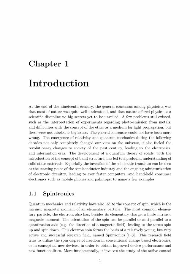
Figure 1.1: Schematic illustration of the GMR and TMR effect, inwhich a parallel alignment of the magnetization of the two ferromagnetic(FM) electrodes has a lower resistance than an anti-parallel alignment.In the case of GMR, the non-magnetic (NM) layer is a metal, in the caseof TMR the NM layer is an insulator.
and manipulation of spin in solid state systems. One key achievement that gavea huge boost to the field is the discovery of the Giant-Magneto-Resistance-effect(GMR-effect) by Albert Fert [4] and Peter Grunberg [5], who have been awardedthe Nobel Prize in Physics of 2007 for their discovery. The GMR-effect enabled thetremendous increase in data storage capabilities of computer hard-disk drives overthe past decade by implementing the effect (within an astonishing ten years afterthe discovery) into a very sensitive magneto-resistive sensor in the read-head of thehard-disk. Another key discovery is the large room-temperature Tunnel-Magneto-Resistance-effect (TMR-effect) in 1995 [6], which nowadays replaces the GMR-effectin sensors, and which might lead to a universal non-volatile solid state memory, themagnetic random access memory (MRAM).
Let us briefly discuss the GMR-effect and TMR-effect in more detail, with thehelp of Fig. 1.1. Consider a tri-layer consisting of two ferromagnetic (FM) materials,separated by a non-magnetic (NM) spacer. In the case of GMR, the non-magneticspacer is a conductor, such as Cu, with a thickness of the order of a few nanometer.The tri-layer is referred to as a spin-valve. The resistance of this structure dependson the relative orientation of the magnetization of the magnetic layers, as a resultof spin dependent scattering of electrons in the magnetic layers. When the electronspin is parallel (anti-parallel) with the magnetization, the scattering probability islow (high), which results is a low (high) resistance. The total current is carried byspin up as well as by spin down electrons. Using the two-channel picture of spintransport, first introduced by Mott, it can be readily seen that a parallel orientationof the magnetization of the two FM layers has a lower total resistance than an anti-parallel orientation. With GMR, the resistance changes that can be achieved withsuch a tri-layer are typically of the order 20%. A crucial aspect in this system isthat the thickness of the non-magnetic spacer layer is lower than the spin scatteringlength, such that spin is conserved when electrons transverse from one magneticlayer to the other. When the non-magnetic spacer layer is an insulator of ≈ 1 − 2
1.2 Semiconductor Spintronics 3
nanometer thickness, it acts as a tunnel barrier. In this case, the tri-layer is referredto as a magnetic tunnel junction. The tunneling rates of spin up and spin downelectrons are (to first order) dependent on the density of filled states in one electrodetimes the density of empty states the other electrode, both at the Fermi level. Withthe presence of the FM layers, these tunneling rates depend on the spin type, andon the relative orientation of the magnetization of the two FM layers. Again, aparallel alignment of the magnetization results in lower resistance than an anti-parallel alignment.
These two systems thus convert magnetic information (the relative orientation ofthe magnetization of the two FM layers) to electric information (via the resistance),which can be processed with standard electronics. Engineering of the propertiesof the FM layers, e.g. via interlayer coupling and exchange bias, have led to thedevelopment of very accurate magnetic field sensors based on the GMR-effect. Also,the record high TMR-values of up to 70% with CoFeB as a magnetic electrode andAlOx as an isolating spacer [7], and well over 500% with CoFeB and MgO [8–10],pave the way for implementing magnetic tunnel junction as memory elements in anon-volatile solid state memory. In combination with a design that uses the so-calledspin transfer torque [11, 12] to switch the magnetization of one of the ferromagneticelectrodes (i.e. the magnetization is switched by a spin polarized current, instead ofwith a magnetic field), this could lead to a universal scalable magnetic solid statememory [13].
Besides the material aspects, also the dynamic properties of the magnetic elec-trodes are important, e.g. in the case of fast switching of the magnetization of theelectrode. Magnetization dynamics at GHz frequencies takes place in the so-calledprecessional regime, which means that the magnetization can only be switched bya precessional motion. The fasted switch possible is that of half a precession pe-riod, called a ballistic switch. Experimentally, ballistic precessional switching viamagnetic field pulses has been demonstrated in micron and sub-micron sized mag-netic elements [14, 15], while similar results are being pursued using spin transferswitching [16, 17]. These achievements form a complementary step towards thedevelopment of magnetic memories.
The above mentioned spin valve and magnetic tunnel junction are examples ofmetallic spintronic applications. In order to fully utilize the spin degree of free-dom in conventional electronics, a spin polarization must be created, manipulated,transported, and detected in conventional semiconductors. The research field whichstudies these aspects is named Semiconductor Spintronics.
1.2 Semiconductor Spintronics
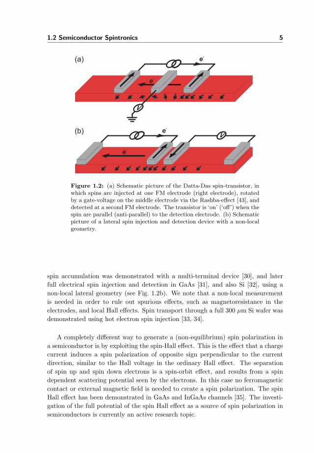
Semiconductor spintronics has the promise of improved device performance overcurrent and future charge-based semiconductor technology [18]. Several proposalsand experimental studies include a spin-FET (field-effect transistor [19, 20], see Fig.
4 Chapter 1 Introduction
1.2a), a spin-LED (light-emitting diode), a spin-RTD (resonant tunneling diode),and quantum bits for quantum computation and communication. Typical ques-tions that are posed in respect of these proposals are: How can a significant spinpolarization be created in a (typically) non-magnetic semiconductor, such as Si orGaAs? How can a spin polarization be efficiently and electrically detected? Whatare the mechanisms for spin relaxation, and can a spin polarization be maintainedlong enough to perform spin manipulation and / or transport? What are ways tomanipulate a spin polarization, in order to obtain device functionality? In the pastdecade an enormous progress has been made in finding solutions to these questions,which we will consider in more detail below.
Spin injection and detection
The oldest and most easiest way to create a non-equilibrium spin polarization in anon-magnetic semiconductor is by optical means [21]. Circularly polarized photonscan transfer angular momentum to the semiconductor via the optical selection rulesof direct band-gap semiconductors, thereby exciting more electrons of one spin typethan of the other. However, for device applications it is desirable to have an electri-cal method for creating a spin polarization, which is often referred to as electricalspin injection. First attempts were based on depositing ferromagnetic contacts onInAs. InAs is one of the few semiconductors with an ideal interface to a transitionmetal, resulting in low Ohmic contacts without Schottky barrier formation. How-ever, later it was realized that the large difference in conductivity between a FMand a semiconductor results in a low spin injection efficiency, an obstacle referredto as the conductivity mismatch [22]. Using semiconductors as a source of spinpolarization, either via spin splitting in a large magnetic field [23], or by using a fer-romagnetic semiconductor such as GaMnAs [24], efficient spin injection into GaAscould be achieved at low temperatures and / or high magnetic field. These meth-ods did, however, not allow room temperature spin injection. This conductivitymismatch problem could be circumvented by introducing a tunnel barrier betweenthe FM and semiconductor, which acts as a large spin dependent resistance [25].Indeed, successful electrical spin injection into GaAs has been achieved using aSchottky-barrier [26], and an insulating barrier such as AlOx [27], and MgO [28].To prove successful spin injection, most studies used a LED-structure underneaththe injection electrode, a configuration also referred to as spin-LED. The degree ofcircular polarization of the electroluminescence originating from this spin-LED isrelated to the injected spin polarization. More recently, spin injection into Si wasdemonstrated in a similar way [29].
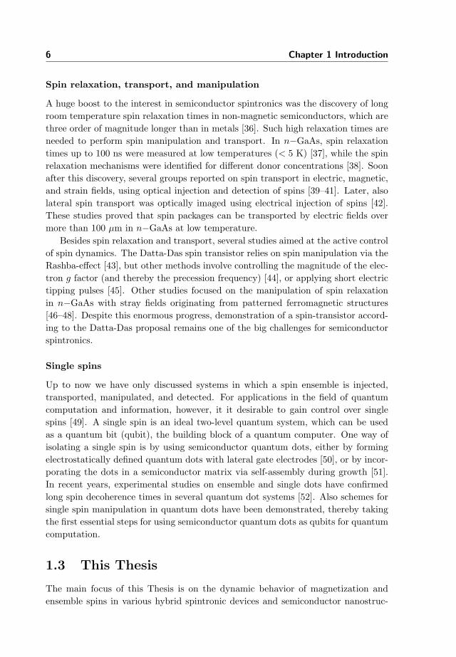
The above demonstrations of spin injection relied, as mentioned, on optical de-tection of light emission from a spin-LED. Naturally, in view of application in de-vices, a more convenient way would be electrical detection of spin injection. Thisis, however, a much more difficult task, because either a lateral geometry of theelectrodes is needed, or spin transport through a full wafer. Electrical detection of
1.2 Semiconductor Spintronics 5
e-
V
e-
e-
e-
V
(a)
(b)
Figure 1.2: (a) Schematic picture of the Datta-Das spin-transistor, inwhich spins are injected at one FM electrode (right electrode), rotatedby a gate-voltage on the middle electrode via the Rashba-effect [43], anddetected at a second FM electrode. The transistor is ‘on’ (‘off’) when thespin are parallel (anti-parallel) to the detection electrode. (b) Schematicpicture of a lateral spin injection and detection device with a non-localgeometry.
spin accumulation was demonstrated with a multi-terminal device [30], and laterfull electrical spin injection and detection in GaAs [31], and also Si [32], using anon-local lateral geometry (see Fig. 1.2b). We note that a non-local measurementis needed in order to rule out spurious effects, such as magnetoresistance in theelectrodes, and local Hall effects. Spin transport through a full 300 µm Si wafer wasdemonstrated using hot electron spin injection [33, 34].
A completely different way to generate a (non-equilibrium) spin polarization ina semiconductor is by exploiting the spin-Hall effect. This is the effect that a chargecurrent induces a spin polarization of opposite sign perpendicular to the currentdirection, similar to the Hall voltage in the ordinary Hall effect. The separationof spin up and spin down electrons is a spin-orbit effect, and results from a spindependent scattering potential seen by the electrons. In this case no ferromagneticcontact or external magnetic field is needed to create a spin polarization. The spinHall effect has been demonstrated in GaAs and InGaAs channels [35]. The investi-gation of the full potential of the spin Hall effect as a source of spin polarization insemiconductors is currently an active research topic.
6 Chapter 1 Introduction
Spin relaxation, transport, and manipulation
A huge boost to the interest in semiconductor spintronics was the discovery of longroom temperature spin relaxation times in non-magnetic semiconductors, which arethree order of magnitude longer than in metals [36]. Such high relaxation times areneeded to perform spin manipulation and transport. In n−GaAs, spin relaxationtimes up to 100 ns were measured at low temperatures (< 5 K) [37], while the spinrelaxation mechanisms were identified for different donor concentrations [38]. Soonafter this discovery, several groups reported on spin transport in electric, magnetic,and strain fields, using optical injection and detection of spins [39–41]. Later, alsolateral spin transport was optically imaged using electrical injection of spins [42].These studies proved that spin packages can be transported by electric fields overmore than 100 µm in n−GaAs at low temperature.
Besides spin relaxation and transport, several studies aimed at the active controlof spin dynamics. The Datta-Das spin transistor relies on spin manipulation via theRashba-effect [43], but other methods involve controlling the magnitude of the elec-tron g factor (and thereby the precession frequency) [44], or applying short electrictipping pulses [45]. Other studies focused on the manipulation of spin relaxationin n−GaAs with stray fields originating from patterned ferromagnetic structures[46–48]. Despite this enormous progress, demonstration of a spin-transistor accord-ing to the Datta-Das proposal remains one of the big challenges for semiconductorspintronics.
Single spins
Up to now we have only discussed systems in which a spin ensemble is injected,transported, manipulated, and detected. For applications in the field of quantumcomputation and information, however, it it desirable to gain control over singlespins [49]. A single spin is an ideal two-level quantum system, which can be usedas a quantum bit (qubit), the building block of a quantum computer. One way ofisolating a single spin is by using semiconductor quantum dots, either by formingelectrostatically defined quantum dots with lateral gate electrodes [50], or by incor-porating the dots in a semiconductor matrix via self-assembly during growth [51].In recent years, experimental studies on ensemble and single dots have confirmedlong spin decoherence times in several quantum dot systems [52]. Also schemes forsingle spin manipulation in quantum dots have been demonstrated, thereby takingthe first essential steps for using semiconductor quantum dots as qubits for quantumcomputation.
1.3 This Thesis
The main focus of this Thesis is on the dynamic behavior of magnetization andensemble spins in various hybrid spintronic devices and semiconductor nanostruc-
1.3 This Thesis 7
tures. We will focus on magnetization dynamics in an MRAM element, and on spinrelaxation and precession in lateral and perpendicular spin injection devices. Also,we will explore the possibilities of optical spin injection in semiconductor nanowires,and try to identify the main spin relaxation mechanism in such wires. Finally, wewill investigate the possibility of controlling the electron or hole g factor in self-assembled semiconductor quantum dots.
This Thesis is organized as follows. In Chapter 2 we will discuss the basic theo-retical aspects of magnetization dynamics in ferromagnetic thin layers, and of spinorientation, relaxation and precession in semiconductors, with a focus on n−dopedGaAs. Chapter 3 gives a description of the measurement techniques used through-out this Thesis, which are for a large part based on the magneto-optical Kerr-effect.This effect is explained in detail, and a model is presented which calculates the Kerr-effect originating from an arbitrary layered structure. This Chapter also presentsunpublished experimental results related to perpendicular magnetized electrodes forspin injection, and measurements of spin relaxation, precession, and diffusion in alateral spin injection device. Precessional magnetization dynamics in a micron sizedferromagnetic element is the subject of Chapter 4. In this Chapter, the questionsrelated to uniform magnetization switching via precessional motion in a potentialMRAM element will be addressed. Chapter 5 is devoted to the determination andunderstanding of electron spin relaxation in a spin-LED under operational con-ditions. The influence of important device parameters, such as carrier densities,temperature, and recombination rate on the spin relaxation rate will be the centraltopic. The potential applicability of semiconductor nanowires as building blocksfor spintronic applications will be investigated in Chapter 6, with the emphasis oncarrier and spin dynamics in these nanowires. We will show that by using micro-scopic techniques, it is possible to optically study individual nanowires. Chapter 7concludes this Thesis and is dedicated to spin relaxation and precession of electronsand holes in self-assembled semiconductor quantum dots. The central question is ifit is possible to control the electron or hole g factor by changing the internal electricfield.
8 Chapter 1 Introduction
Bibliography
[1] S. A. Wolf, D. D. Awschalom, R. A. Buhrman, J. M. Daughton, S. von Molnar,M. L. Roukes, A. Y. Chtchelkanova, and D. M. Treger, Spintronics: A spin-based electronics vision for the future, Science 294, 1488-1495 (2001). 1.1
[2] I. Zutic, J. Fabian, S. Das Sarma, Spintronics: Fundamentals and applications,Rev. Mod. Phys. 76, 323-410 (2004).
[3] C. Chappert, A. Fert, and Frederic Nguyen Van Dau, The emergence of spinelectronics in data storage, Nat. Mater. 6, 813-823 (2007). 1.1
[4] M. N. Baibich, J. M. Broto, A. Fert, F. Nguyen Van Dau, F. Petroff, P.Eitenne, G. Creuzet, A. Friederich, and J. Chazelas, Giant magnetoresistance of(001)Fe/(001)Cr magnetic superlattices, Phys. Rev. Lett. 61, 2472-2475 (1988).1.1
[5] G. Binasch, P. Grunberg, F. Saurenbach, and W. Zinn, Enhanced magnetore-sistance in layered magnetic structures with antiferromagnetic interlayer ex-change, Phys. Rev. B 39, 4828-4830 (1989). 1.1
[6] J. S. Moodera, L. R. Kinder, T. M. Wong, and R. Meservey, Large magnetore-sistance at room temperature in ferromagnetic thin film tunnel junctions, Phys.Rev. Lett. 74, 3273-3276 (1995). 1.1
[7] D. Wang, C. Nordman, J. M. Daughton, Z. Qian, and J. Fink, 70% TMR atroom temperature for SDT sandwich junctions with CoFeB as free and referencelayers, IEEE Trans. Magn. 40, 2269-2271 (2004). 1.1
[8] S. S. P. Parkin, C. Kaiser, A. Panchula, P. M. Rice, B. Hughes, M. Samant,and S.-H. Yang, Giant tunnelling magnetoresistance at room temperature withMgO (100) tunnel barriers, Nat. Mater. 3, 862-867 (2004). 1.1
[9] S. Yuasa, T. Nagahama, A. Fukushima, Y. Suzuki, and K. Ando, Giant room-temperature magnetoresistance in single-crystal Fe/MgO/Fe magnetic tunneljunctions, Nat. Mater. 3, 868-871 (2004).
[10] S. Ikeda, J. Hayakawa, Y. Ashizawa, Y. M. Lee, K. Miura, H. Hasegawa, M.Tsunoda, F. Matsukura, and H. Ohno, Tunnel magnetoresistance of 604% at300 K by suppression of Ta diffusion in CoFeB/MgO/CoFeB pseudo-spin-valvesannealed at high temperature, Appl. Phys. Lett. 93, 082508 (2008). 1.1
[11] J. C. Slonczewski, Current-driven excitation of magnetic multilayers, J. Magn.Magn. Mater. 159, L1-L7 (1996). 1.1
[12] L. Berger, Emission of spin waves by a magnetic multilayer transversed by acurrent, Phys. Rev. B 54, 9353-9358 (1996). 1.1
BIBLIOGRAPHY 9
[13] T. Kawahara, R. Takemura, K. Miura, J. Hayakawa, S. Ikeda, Y. M. Lee, R.Sasaki, Y. Goto, K. Ito, T. Meguro, F. Matsukura, H. Takahashi, H. Matsuoka,and H. Ohno, 2 Mb SPRAM (SPin-Transfer Torque RAM) With Bit-by-Bit Bi-Directional Current Write and Parallelizing-Direction Current Read, IEEE J.Sol. St. Circ. 43, 109 (2008). 1.1
[14] Th. Gerrits, H. A. M. van den Berg, J. Hohlfeld, L. Bar, and Th. Rasing,Ultrafast precessional magnetization reversal by picosecond magnetic field pulseshaping, Nature (London) 418, 509-512 (2002). 1.1
[15] H. W. Schumacher, C. Chappert, R. C. Sousa, P. P. Freitas, and J. Miltat,Quasiballistic magnetization reversal, Phys. Rev. Lett. 90, 017204 (2003). 1.1
[16] T. Devolder, J. Hayakawa, K. Ito, H. Takahashi, S. Ikeda, P. Crozat, N. Zer-ounian, Joo-Von Kim, C. Chappert, and H. Ohno, Single-Shot Time-ResolvedMeasurements of Nanosecond-Scale Spin-Transfer Induced Switching: Stochas-tic Versus Deterministic Aspects, Phys. Rev. Lett. 100, 057206 (2008). 1.1
[17] S. Serrano-Guisan, K. Rott, G. Reiss, J. Langer, B. Ocker, and H. W. Schu-macher, Biased Quasiballistic Spin Torque Magnetization Reversal, Phys. Rev.Lett. 101, 087201 (2008). 1.1
[18] D. D. Awschalom, and M. Flatte, Challenges for semiconductor spintronics,Nat. Phys. 3, 153-159 (2007). 1.2
[19] S. Datta, and B. Das, Electronic analog of the electrooptic modulator, Appl.Phys. Lett. 56, 665-667 (1990). 1.2
[20] K. C. Hall, W. H. Lau, K. Gundogdu, M. E. Flatte, and T. F. Boggess, Nonmag-netic semiconductor spin transistor, Appl. Phys. Lett. 83, 2937-2939 (2003). 1.2
[21] Optical Orientation (Modern Problems in Condensed Matter Sciences, Vol. 8),edited by F. Meier, and B. P. Zachachrenya (North-Holland, Amsterdam, 1984).1.2
[22] G. Schmidt, D. Ferrand, L. W. Molenkamp, A. T. Filip, and B. J. van Wees,Fundamental obstacle for electrical spin injection from a ferromagnetic metalinto a diffusive semiconductor, Phys. Rev. B 62, R4790-R4793 (2000). 1.2
[23] R. Fiederling, M. Kleim, G. Reuscher, W. Ossau, G. Schmidt, A. Waag, and L.W. Molenkamp, Injection and detection of a spin-polarized current in a light-emitting diode, Nature (London) 402, 787-790 (1999). 1.2
[24] Y. Ohno, D. K. Young, B. Beschoten, F. Matsukura, H. Ohno, and D. D.Awschalom, Electrical spin injection in a ferromagnetic semiconductor het-erostructure, Nature (London) 402, 790-792 (1990). 1.2
10 Chapter 1 Introduction
[25] E. I. Rashba, Theory of electrical spin injection: Tunnel contacts as a solutionof the conductivity mismatch problem, Phys. Rev. B 62, R16267-R16270 (2000).1.2
[26] A. T. Hanbicki, B. T. Jonker, G. Itskos, G. Kioseoglou, and A. Petrou, Efficientelectrical spin injection from a magnetic metal/tunnel barrier contact into asemiconductor, Appl. Phys. Lett. 80, 1240-1242 (2002). 1.2
[27] V. F. Motsnyi, V. I. Safarov, J. De Boeck, J. Das, W. Van Roy, E.Goovaerts, and G. Borghs, Electrical spin injection in a ferromagnet/tunnelbarrier/semiconductor heterostructure, Appl. Phys. Lett. 81, 265-267 (2002).1.2
[28] X. Jiang, R. Wang, R. M. Shelby, R. M. Macfarlane, S. R. Bank, J. S. Harris,and S. S. P. Parkin, Highly spin-polarized room-temperature tunnel injector forsemiconductor spintronics using MgO(100), Phys. Rev. Lett. 94, 056601 (2005).1.2
[29] B. T. Jonker, G. Kioseoglou, A. T. Hanbicki, C. H. Li, and P. E. Thompson,Electrical spin-injection into silicon from a ferromagnetic metal/tunnel barriercontact, Nat. Phys. 3, 542 (2007). 1.2
[30] X. Lou, C. Adelmann, M. Furis, S. A. Crooker, C. J. Palmstrøm, andP. A. Crowell, Electrical detection of spin accumulation at a ferromagnet-semiconductor interface. Phys. Rev. Lett. 96, 176603 (2006). 1.2
[31] X. Lou, C. Adelmann, S. A. Crooker, E. S. Garlid, J. Zhang, K. S. MadhukarReddy, S. D. Flexner, C. J. Palmstrøm, and P. A. Crowell, Electrical detectionof spin transport in lateral ferromagnet-semiconductor devices, Nat. Phys. 3,197-202 (2007). 1.2
[32] O. M. J. van ’t Erve, A. T. Hanbicki, M. Holub, C. H. Li, C. Awo-Affouda,P. E. Thompson, and B. T. Jonker, Electrical injection and detection of spin-polarized carriers in silicon in a lateral transport geometry, Appl. Phys. Lett.91, 212109 (2007). 1.2
[33] I. Appelbaum, B. Huang, and D. Monsma, Electronic measurement and controlof spin transport in silicon, Nature (London) 447, 295 (2007). 1.2
[34] B. Huang, D. Monsma, and I. Appelbaum, Coherent Spin Transport through a350 Micron Thick Silicon Wafer, Phys. Rev. Lett. 99, 177209 (2007) 1.2
[35] Y. K. Kato, R. C. Myers, A. C. Gossard, and D. D. Awschalom, Observationof the spin Hall effect in semiconductors, Science 306, 1910-1913 (2004). 1.2
[36] J. M. Kikkawa, I. P. Smorchkova, N. Samarth, and D. D. Awschalom, Room-temperature spin memory in two-dimensional electron gases, Science 277, 1284-1287 (1997). 1.2
BIBLIOGRAPHY 11
[37] J. M. Kikkawa, and D. D. Awschalom, Resonant spin amplification in n-typeGaAs, Phys. Rev. Lett. 80, 4313-4316 (1998). 1.2
[38] R. I. Dzhioev, K. V. Kavokin, V. L. Korenev, M. V. Lazarev, B. Y. Meltser,M. N. Stepanova, B. P. Zakharchenya, D. Gammon, and D. S. Katzer, Low-temperature spin relaxation in n-type GaAs, Phys. Rev. B 66, 245204 (2002).1.2
[39] J. M. Kikkawa, and D. D. Awschalom, Lateral drag of spin coherence in galliumarsenide, Nature (London) 397, 139-141 (1999). 1.2
[40] Y. K. Kato, R. C. Myers, A. C. Gossard, and D. D. Awschalom, Coherentspin manipulation without magnetic fields in strained semiconductors, Nature(London) 427, 50-53 (2004).
[41] S. A. Crooker, and D. L. Smith, Imaging spin flows in semiconductors subjectto electric, magnetic, and strain fields, Phys. Rev. Lett. 94, 236601 (2005). 1.2
[42] S. A. Crooker, M. Furis, X. Lou, C. Adelmann, D. L. Smith, C. J. Palmstrøm,and P. A. Crowell, Imaging spin transport in lateral ferromagnet/semiconductorstructures, Science 309, 2191-2195 (2005). 1.2
[43] Yu. A. Bychkov, and E. I. Rashba, Oscillatory effects and the magnetic sus-ceptibility of carriers in inversion layers, J. Phys. C: Solid State Phys. 17,6039-6045 (1984). 1.2, 1.2
[44] G. Salis, Y. Kato, K. Ensslin, D. C. Driscoll, A. C. Gossard, and D. D.Awschalom, Electrical control of spin coherence in semiconductor nanostruc-tures, Nature (London) 414, 619-622 (2001). 1.2
[45] Y. Kato, R. C. Myers, D. C. Driscoll, A. C. Gossard, J. Levy, and D. D.Awschalom, Gigahertz electron spin manipulation using voltage-controlled g-tensor modulation, Science 299, 1201-1204 (2003). 1.2
[46] L. Meiera, G. Salis, C. Ellenberger, K. Ensslin, and E. Gini, Stray-field-inducedmodification of coherent spin dynamics, Appl. Phys. Lett. 88, 172501 (2006).1.2
[47] S. Halma, G. Bacher, E. Schuster, W. Keune, M. Sperl, J. Puls, and F. Hen-neberger, Local spin manipulation in ferromagnet-semiconductor hybrids, Appl.Phys. Lett. 90, 051916 (2007).
[48] P. E. Hohage, J. Nannen, S. Halm, G. Bacher, M. Wahle, S. F. Fischer, U.Kunze, D. Reuter, and A. D. Wieck, Coherent spin dynamics in Permalloy-GaAs hybrids at room temperature, Appl. Phys. Lett. 92, 241920 (2008). 1.2
[49] D. Loss, and D. P. DiVincenzo, Quantum computation with quantum dots, Phys.Rev. A 57, 120-122 (1998). 1.2
12 Chapter 1 Introduction
[50] R. Hanson, L. P. Kouwenhoven, J. R. Petta, S. Tarucha, and L. M. K. Van-dersypen, Spins in few-electron quantum dots, Rev. Mod. Phys. 79, 1217-1265(2007). 1.2
[51] M. S. Skolnick, and D. J. Mowbray, Self-assembled semiconductor quantumdots: Fundamental Physics and Device Applications, Annu. Rev. Mater. Res.34, 181-218 (2004). 1.2
[52] M. Paillard, X. Marie, P. Renucci, T. Amand, A. Jbeli, and J. M. Gerard, SpinRelaxation Quenching in Semiconductor Quantum Dots, Phys. Rev. Lett. 86,1634 (2001). 1.2
Chapter 2
Magnetization and spindynamics
This Chapter discusses the main physical processes and phenomena that are needed
to explain and discuss experimental data in Chapters 3 to 7, but which are not
treated in depth in these Chapters. We will first discuss the general concepts of
magnetization precession and spin waves in ferromagnets, which we will encounter
in Chapter 4. Next, we will focus on optical spin orientation in semiconductors,
and the main spin relaxation mechanisms in bulk and quantum systems, which will
be important in Chapters 5-7. Special attention will be given to spin relaxation in
bulk n−GaAs. The final topic is spin precession and dephasing in semiconductors,
which will be relevant in Chapters 3 and 7.
13
14 Chapter 2 Magnetization and spin dynamics
2.1 Magnetization dynamics in ferromagnets
The magnetization of a ferromagnet is a local quantity that describes in which di-rection an ensemble of local magnetic moments (spins) is aligned. The direction ofthis magnetization can usually be changed by applying a magnetic field. A strongmagnetic field will in general align all the magnetic moments of a ferromagnet inthe same direction, a situation which is called saturation. In magnetic storage de-vices, such as hard disk-drives or magnetic random access memory, the binary datais stored as the parallel or anti-parallel alignment of the magnetization directionwith respect to a preset axis in small magnetic grains or elements. Nowadays, it isrequired that the writing of the data, and thus the switching of the magnetization,occurs on a (sub-)nanosecond time-scale. On this timescale, the magnetization dy-namics in ferromagnets is governed by the Landau-Lifshitz-Gilbert (LLG) equation[1–3]. This equation describes the motion of the local magnetization vector, andtakes the following form
d~m(~x, t)dt
= γµ0
(~m(~x, t)× ~Heff (~x, t)
)+
α
Ms
(~m(~x, t)× d~m(~x, t)
dt
). (2.1)
Here, ~m(~x, t) = ~M(~x, t)/Ms is the normalized local magnetization vector, γ the gy-romagnetic ratio (γ = g e
2me, with g the gyromagnetic splitting factor of the electron
in the magnetic material, and e and me the electron charge and mass respectively),µ0 the magnetic permeability of vacuum and ~Heff (~x, t) the local effective magneticfield, Ms the saturation magnetization, and α a phenomenological (Gilbert) param-eter, which is a measure of the damping in the system [2, 3]. This equation statesthat the local effective magnetic field exerts a torque on the local magnetization,and that this torque is responsible for the motion of the magnetization. This motionis a precessional motion around the local effective field, since the direction of thetorque is perpendicular to both the magnetization vector, and the local effectivefield. Depending on the value of α, the precessional motion can be over-damped,critically damped or under-damped. In most cases with thin magnetic layers, α ¿ 1,and the motion is in the under-damped regime, leading to many revolutions of themagnetization vector (also called ringing). The local effective field is the sum ofseveral different fields, which include the exchange field, the dipole field (or demag-netizing field), crystalline and shape anisotropy, coupling fields from neighboringlayers (via exchange bias or interlayer coupling), and the externally applied mag-netic field. In particular, the exchange and dipole field give rise to short and longrange interactions, respectively, between local magnetic moments, and can therebyinduce spin-waves [4]. We will not discuss all the aspects of spin waves in detail, butstate here three important classes of lateral spin waves encountered in thin magneticelements. These classes are defined by the relative orientation of the magnetization~M , the wavevector, ~q, of the spin wave, and the normal of the sample plane ~n.For ~n ‖ ~M ⊥ ~q, we have the so-called forward volume magnetostatic mode , for~n ⊥ ~M ⊥ ~q, it is the Damon-Eshbach surface mode [5], and for ~n ⊥ ~M ‖ ~q, the spin
2.1 Magnetization dynamics in ferromagnets 15
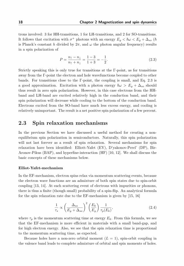
y
x
z
Hbias Mt=0Py Hbias
Hpulse Mt=t1
Py
Heff
Hdem
Mt=0
t = 0 t = t 1
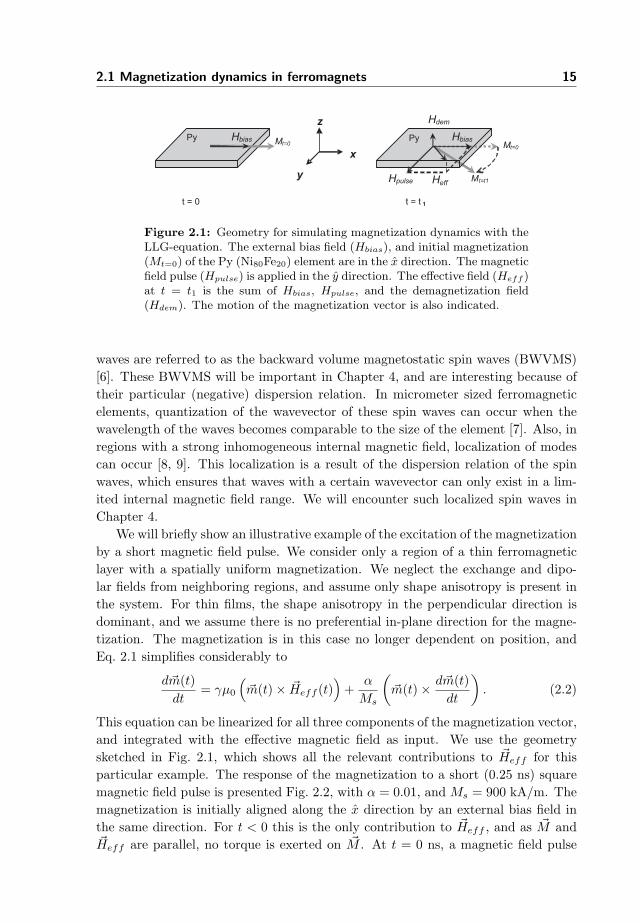
Figure 2.1: Geometry for simulating magnetization dynamics with theLLG-equation. The external bias field (Hbias), and initial magnetization(Mt=0) of the Py (Ni80Fe20) element are in the x direction. The magneticfield pulse (Hpulse) is applied in the y direction. The effective field (Heff )at t = t1 is the sum of Hbias, Hpulse, and the demagnetization field(Hdem). The motion of the magnetization vector is also indicated.
waves are referred to as the backward volume magnetostatic spin waves (BWVMS)[6]. These BWVMS will be important in Chapter 4, and are interesting because oftheir particular (negative) dispersion relation. In micrometer sized ferromagneticelements, quantization of the wavevector of these spin waves can occur when thewavelength of the waves becomes comparable to the size of the element [7]. Also, inregions with a strong inhomogeneous internal magnetic field, localization of modescan occur [8, 9]. This localization is a result of the dispersion relation of the spinwaves, which ensures that waves with a certain wavevector can only exist in a lim-ited internal magnetic field range. We will encounter such localized spin waves inChapter 4.
We will briefly show an illustrative example of the excitation of the magnetizationby a short magnetic field pulse. We consider only a region of a thin ferromagneticlayer with a spatially uniform magnetization. We neglect the exchange and dipo-lar fields from neighboring regions, and assume only shape anisotropy is present inthe system. For thin films, the shape anisotropy in the perpendicular direction isdominant, and we assume there is no preferential in-plane direction for the magne-tization. The magnetization is in this case no longer dependent on position, andEq. 2.1 simplifies considerably to
d~m(t)dt
= γµ0
(~m(t)× ~Heff (t)
)+
α
Ms
(~m(t)× d~m(t)
dt
). (2.2)
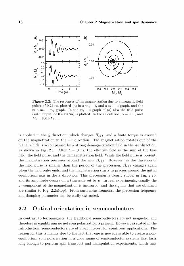
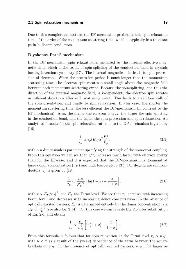
This equation can be linearized for all three components of the magnetization vector,and integrated with the effective magnetic field as input. We use the geometrysketched in Fig. 2.1, which shows all the relevant contributions to ~Heff for thisparticular example. The response of the magnetization to a short (0.25 ns) squaremagnetic field pulse is presented Fig. 2.2, with α = 0.01, and Ms = 900 kA/m. Themagnetization is initially aligned along the x direction by an external bias field inthe same direction. For t < 0 this is the only contribution to ~Heff , and as ~M and~Heff are parallel, no torque is exerted on ~M . At t = 0 ns, a magnetic field pulse
16 Chapter 2 Magnetization and spin dynamics
-0.01
0.00
0.01
-0.2 -0.1 0.0 0.1 0.2 0.3
-0.01
0.00
0.01
0 1 2 3 4
-0.2-0.10.00.10.20.3
Mz /
Ms
My /
Ms
Time (ns)
b)a)
My / Ms
Mz /
Ms
Figure 2.2: The responses of the magnetization due to a magnetic fieldpulses of 0.25 ns, plotted (a) in a my − t, and a mz − t graph, and (b)in a mz − my graph. In the my − t graph of (a) also the field pulse(with amplitude 0.4 kA/m) is plotted. In the calculation, α = 0.01, andMs = 900 kA/m.
is applied in the y direction, which changes ~Heff , and a finite torque is exertedon the magnetization in the −z direction. The magnetization rotates out of theplane, which is accompanied by a strong demagnetization field in the +z direction,as shown in Fig. 2.1. After t = 0 ns, the effective field is the sum of the biasfield, the field pulse, and the demagnetization field. While the field pulse is present,the magnetization precesses around the new ~Heff . However, as the duration ofthe field pulse is smaller than the period of the precession, ~Heff changes againwhen the field pulse ends, and the magnetization starts to precess around the initialequilibrium axis in the x direction. This precession is clearly shown in Fig. 2.2b,and its amplitude decays on a timescale set by α. In real experiments, usually thez−component of the magnetization is measured, and the signals that are obtainedare similar to Fig. 2.2a(top). From such measurements, the precession frequencyand damping parameter can be easily extracted.
2.2 Optical orientation in semiconductors
In contrast to ferromagnets, the traditional semiconductors are not magnetic, andtherefore in equilibrium no net spin polarization is present. However, as stated in theIntroduction, semiconductors are of great interest for spintronic applications. Thereason for this is mainly due to the fact that one is nowadays able to create a non-equilibrium spin polarization in a wide range of semiconductor systems that lastslong enough to perform spin transport and manipulation experiments, which may
2.2 Optical orientation in semiconductors 17
E
k
CB
HH
LH
SO
S1/2
P3/2
P1/2
Eg
Dso
1/2 3/2
1/2
-3/2 -1/2
-1/2
-1/2 1/2
HH, LH
SO
CB
s+
s+
s+
s-
s-
s-
1
2
3 3
2
1
mj
mj
mj
(a) (b)
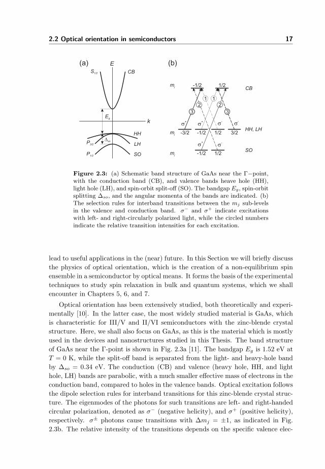
Figure 2.3: (a) Schematic band structure of GaAs near the Γ−point,with the conduction band (CB), and valence bands heave hole (HH),light hole (LH), and spin-orbit split-off (SO). The bandgap Eg, spin-orbitsplitting ∆so, and the angular momenta of the bands are indicated. (b)The selection rules for interband transitions between the mj sub-levelsin the valence and conduction band. σ− and σ+ indicate excitationswith left- and right-circularly polarized light, while the circled numbersindicate the relative transition intensities for each excitation.
lead to useful applications in the (near) future. In this Section we will briefly discussthe physics of optical orientation, which is the creation of a non-equilibrium spinensemble in a semiconductor by optical means. It forms the basis of the experimentaltechniques to study spin relaxation in bulk and quantum systems, which we shallencounter in Chapters 5, 6, and 7.
Optical orientation has been extensively studied, both theoretically and experi-mentally [10]. In the latter case, the most widely studied material is GaAs, whichis characteristic for III/V and II/VI semiconductors with the zinc-blende crystalstructure. Here, we shall also focus on GaAs, as this is the material which is mostlyused in the devices and nanostructures studied in this Thesis. The band structureof GaAs near the Γ-point is shown in Fig. 2.3a [11]. The bandgap Eg is 1.52 eV atT = 0 K, while the split-off band is separated from the light- and heavy-hole bandby ∆so = 0.34 eV. The conduction (CB) and valence (heavy hole, HH, and lighthole, LH) bands are parabolic, with a much smaller effective mass of electrons in theconduction band, compared to holes in the valence bands. Optical excitation followsthe dipole selection rules for interband transitions for this zinc-blende crystal struc-ture. The eigenmodes of the photons for such transitions are left- and right-handedcircular polarization, denoted as σ− (negative helicity), and σ+ (positive helicity),respectively. σ± photons cause transitions with ∆mj = ±1, as indicated in Fig.2.3b. The relative intensity of the transitions depends on the specific valence elec-
18 Chapter 2 Magnetization and spin dynamics
trons involved: 3 for HH-transitions, 1 for LH-transitions, and 2 for SO-transitions.It follows that excitation with σ+ photons with an energy Eg < ~ω < Eg + ∆so (~is Planck’s constant h divided by 2π, and ω the photon angular frequency) resultsin a spin polarization of
P =n↑ − n↓n↑ + n↓
=1− 31 + 3
= −12. (2.3)
Strictly speaking this is only true for transitions at the Γ-point, as for transitionsaway from the Γ-point the electron and hole wavefunctions become coupled to otherbands. For transitions close to the Γ-point, the coupling is small, and Eq. 2.3 isa good approximation. Excitation with a photon energy ~ω > Eg + ∆so shouldthus result in zero spin polarization. However, in this case electrons from the HH-band and LH-band are excited relatively high in the conduction band, and theirspin polarization will decrease while cooling to the bottom of the conduction band.Electrons excited from the SO-band have much less excess energy, and cooling isrelatively unimportant. The result is a net positive spin polarization of a few percent.
2.3 Spin relaxation mechanisms
In the previous Section we have discussed a useful method for creating a non-equilibrium spin polarization in semiconductors. Naturally, this spin polarizationwill not last forever as a result of spin relaxation. Several mechanisms for spinrelaxation have been identified: Elliott-Yafet (EY), D’yakonov-Perel’ (DP), Bir-Aronov-Pikus (BAP), and hyperfine-interaction (HF) [10, 12]. We shall discuss thebasic concepts of these mechanisms below.
Elliot-Yafet-mechanism
In the EF-mechanism, electron spins relax via momentum scattering events, becausethe electron wave functions are an admixture of both spin states due to spin-orbitcoupling [13, 14]. At each scattering event of electrons with impurities or phonons,there is thus a finite (though small) probability of a spin-flip. An analytical formulafor the spin relaxation rate due to the EF-mechanism is given by [15, 16]
1τs∝
(∆so
Eg + ∆so
)2 (Ek
Eg
)1
τp(Ek), (2.4)
where τp is the momentum scattering time at energy Ek. From this formula, we seethat the EF-mechanism is more efficient in materials with a small band-gap, andfor high electron energy. Also, we see that the spin relaxation time is proportionalto the momentum scattering time, as expected.
Because holes have a non-zero orbital moment (L = 1), spin-orbit coupling inthe valence band leads to complete admixture of orbital and spin moments of holes.
2.3 Spin relaxation mechanisms 19
Due to this complete admixture, the EF-mechanism predicts a hole spin relaxationtime of the order of the momentum scattering time, which is typically less than oneps in bulk-semiconductors.
D’yakonov-Perel’-mechanism
In the DP-mechanism, spin relaxation is mediated by the internal effective mag-netic field, which is the result of spin-splitting of the conduction band in crystalslacking inversion symmetry [17]. The internal magnetic field leads to spin preces-sion of electrons. When the precession period is much longer than the momentumscattering time, the electron spin rotates a small angle about the magnetic fieldbetween each momentum scattering event. Because the spin-splitting, and thus thedirection of the internal magnetic field, is k-dependent, the electron spin rotatesin different directions after each scattering event. This leads to a random walk ofthe spin orientation, and finally to spin relaxation. In this case, the shorter themomentum scattering time, the less efficient the DP-mechanism (in contrast to theEF-mechanism). Also, the higher the electron energy, the larger the spin splittingin the conduction band, and the faster the spin precession and spin relaxation. Ananalytical formula for the spin relaxation rate due to the DP-mechanism is given by[16]
1τs∝ τp(Ek)α2 E3
k
Eg, (2.5)
with α a dimensionless parameter specifying the strength of the spin-orbit coupling.From this equation we can see that 1/τs increases much faster with electron energythan for the EF-case, and it is expected that the DP-mechanism is dominant atlarge donor concentration (nD) and high temperature (T ). For degenerate semicon-ductors, τp is given by [18]
1τp∝ nD
E3/2F
[ln(1 + x)− x
1 + x
], (2.6)
with x ∝ EF /n1/3D , and EF the Fermi level. We see that τp increases with increasing
Fermi level, and decreases with increasing donor concentration. In the absence ofoptically excited carriers, EF is determined entirely by the donor concentration, viaEF ∝ n
2/3D (see also Eq. 2.14). For this case we can rewrite Eq. 2.5 after substitution
of Eq. 2.6, and obtain
1τs∝ Eg
n2D
[ln(1 + x)− x
1 + x
]. (2.7)
From this formula it follows that for spin relaxation at the Fermi level τs ∝ n−νD ,
with ν < 2 as a result of the (weak) dependence of the term between the squarebrackets on nD. In the presence of optically excited carriers, ν will be larger as
20 Chapter 2 Magnetization and spin dynamics
a result of the explicit dependence of τp on EF (which increases with increasingexcitation density). We shall implement the DP-mechanism in the case of n−GaAs,together with carrier recombination, in a model that calculates the time evolutionof a spin distribution after optical orientation. This is described in the next Section.
Bir-Aronov-Pikus-mechanism
In the BAP-mechanism, electron scattering with holes involving spin flip is thedominant process [19, 20]. This process is mediated by the electron-hole exchangeinteraction. The spin-flip scattering probability depends on the state of the holes(bound to acceptors or free, non-degenerate or degenerate, fast or slow). For thecase of non-degenerate holes, and including both bound and free holes, the spinrelaxation rate is given by
1τs∝
¯< D2s >
EB
ve
vB
(nAa3
B
)(p
nA|ψ(0)|4 +
53
nA − p
nA
), (2.8)
with Ds the exchange constant, EB and aB the Bohr-energy, and -radius for theexciton respectively, vB = ~
meaB, and me and ve the electron effective mass and
velocity, respectively. p is the free hole density, nA the acceptor density (and thusthe density of bound holes), while |ψ(0)|2 is the Sommerfield-factor, which is ameasure for the screening of the Coulomb-potential between the electron and hole.
For the case of degenerate holes, and fast electrons (ve > vF , with vF the Fermi-velocity of the holes), the spin relaxation rate is given by
1τs∝
¯< D2s >
EB
ve
vB
(pa3
B
) T
EF|ψ(0)|4. (2.9)
The strength of the BAP-mechanism depends on the hole density according to1/τs ∼ nA for non-degenerate holes (Eq. 2.8), and according to 1/τs ∼ p1/3 fordegenerate holes (Eq. 2.9, with EF ∝ p2/3, see also Eq. 2.14). In the intermediateregime only a weak dependence on p is observed. The temperature dependenceof τs for degenerate holes is given by Eq. 2.9, from which it follows that (withve =
√3kBT/me, kB Boltzmann’s constant) 1/τs ∝ T 3/2. Measurements of the
temperature dependence of τs in GaAs by Aronov et al. [16], could be well describedby the expression
1/τs = 2.3 · p1/3T 3/2, (2.10)
with τs in seconds, p in cm−3 and T in Kelvin. We will use this equation in Chapter5 to compare our data with the theoretical predictions. We note that BAP is thedominant mechanism in heavily p−doped samples at relatively low temperatures.Due to the strong energy dependence in the DP-mechanism, spin relaxation via DPwill dominate at high temperature, even at high acceptor concentrations.
2.4 Modeling spin relaxation in n−GaAs 21
Hyperfine-interaction
Finally, in the HF-mechanism, the combined random magnetic moments of nucleilead to a fluctuating magnetic field experienced by localized or confined electrons.The HF-mechanism is too weak in bulk semiconductors to be dominant over EYand DP, due to the itinerant nature of the electrons. It is, however, an importantmechanism for single-spin decoherence of localized electrons, e.g. electrons confinedin quantum dots or bound to donors. For these electrons, the DP mechanism issuppressed, leading to very large spin relaxation times.
2.4 Modeling spin relaxation in n−GaAs
Spin relaxation in n−GaAs is extensively studied during the last decades, followingthe discovery of large spin relaxation times exceeding 100 ns for moderate dopinglevels [18, 21]. For donor concentrations above the metal-insulator transition (thus >
2·1016 cm−3) the spin relaxation is mediated by the DP-mechanism. In Chapter 3 wewill discuss the experimental technique used in this Thesis to study spin relaxationin several devices and semiconductor nanostructures. An example, presented tooutline the capabilities of the technique, involves a semiconductor heterostructurewith a n−GaAs transport channel. Here, we will present a simple model to describespin relaxation in n−GaAs as a function of excitation density, including the effectof recombination.
In order to model the spin relaxation in a n−GaAs layer, we will assume a uni-form doping profile, and uniform carrier excitation. Also, we will set the temperatureto T = 0. The electron density due to doping is equal to the donor concentration,nD, while the density of electrons due to laser excitation is nL. Following the opticalselection rules for zinc-blende crystal structures, the spin up density, n↑, right afterlaser excitation is given by n↑ = 1
2nD + 34nL, while the spin down density, n↓, is
given by n↓ = 12nD + 1
4nL. The bar indicates the total spin up and spin down den-sity respectively, i.e. integrated over all electron energies in the conduction band.The situation after laser excitation and thermalization is schematically shown inFig. 2.4. We are interested in the net electron spin moment, S, as a function of timeafter laser excitation, which is given in units of ~/2 by
S(t) = n↑(t)− n↓(t) =
EF↑(t)∫
Eg
n(E)dE −EF↓(t)∫
Eg
n(E)dE. (2.11)
Here, n(E) is the density of states function in the conduction band, while EF,↑(↓)(t)represent the time-dependent electron quasi-Fermi level for spin up (down) electrons.When the electron quasi-Fermi level for spin up and spin down electrons is different,there will be a net flow of majority spins to minority spins due to spin relaxation,until the electron quasi-Fermi level of each spin band is equal, and the net spin

22 Chapter 2 Magnetization and spin dynamics
E
n(E)
ts(E)
rr rr
EF
EF
(a) (b)
Figure 2.4: (a) Schematic representation of the spin dependent den-sity of states after laser excitation in n−GaAs. The conduction band(CB), valence band (VB), and the processes of spin relaxation and re-combination are indicated. τs is the spin relaxation time, rr representsthe recombination parameter. (b) Spin relaxation time as a function ofdonor concentration in GaAs, adapted from [18]. The DP-calculation for1016 < nD < 1019 can be approximated with τs ∝ n−1.77
D .
moment is zero. Spin flip events of both spin up and spin down electrons take placeat all electron energies, and since spin relaxation is mediated by the DP-mechanism,the spin flip rate depends strongly on the electron energy. In the following we willpresent the equations of the model for only the spin up density. The spin downdensity is found by interchanging the ↑’s and ↓’s. The rate equation for the spin updensity is given by
dn↑(t)dt
= −EF↑(t)∫
Eg
n(E)τs(E)
dE +
EF↓(t)∫
Eg
n(E)τs(E)
dE. (2.12)
The first term on the right hand side represents the loss of spin up electrons dueto spin flips, while the second term represents the gain of spin up electrons due tospin flips of spin down electrons. τs(E) is the energy dependent spin relaxation timeaccording to the DP-mechanism. In order to carry out the integrals, it is convenientto express the total spin density in terms of the (time-dependent) electron quasi-Fermi level. From the formula for the 3D density of states in the conduction band,
n(E) = 8π√
2(me
h2
)3/2 √E − Eg = n0
√E − Eg, (2.13)

2.4 Modeling spin relaxation in n−GaAs 23
with n0 a constant introduced for convenience, it follows that
n↑(EF↑(t)) =
EF↑(t)∫
Eg
n(E)dE =23n0 (EF↑(t)− Eg)
3/2. (2.14)
We take the dependence of τs on nD, as presented by Dzhioev et al. [18], to calculatethe spin flip time for each electron energy. Their theoretical estimation can beapproximated by
τs(nD) = cDn−1.77D , (2.15)
with cD a constant which has the numerical value 1.23 · 1022 if nD is expressedin units of cm−3. As mentioned in the previous Section, the absolute value of theexponent of nD is slightly smaller than 2 in the absence of optically excited carriers.However, for simplicity we will also use this expression in the presence of opticallyexcited carriers, and replace nD with (nD + nL). In doing so, we underestimatethe electron spin relaxation rate at high excitation density. In the experimentsof Dzhioev et al. the electron quasi-Fermi levels of both sub-bands after opticalorientation are nearly equal, and close to the equilibrium Fermi level. This meansthat electron spin relaxation takes place at the equilibrium Fermi level. Therefore,we can replace the donor concentration nD with the electron (spin up or spin down)concentration, and use Eq. 2.14 with EF↑ = E, to express τs as a function of energy,yielding
τs(E) = cD
(23n0
)−1.77
(E − Eg)−2.66
. (2.16)
Substituting Eqs. 2.13, 2.14, and 2.16 in Eq. 2.12, carrying out the integrals, rear-ranging, and setting Eg = 0 (which does not affect the calculation), results in
dEF↑(t)dt
=
(23n0
)1.77 (−EF↑(t)4.16 + EF↓(t)4.16)
4.16cD
√EF↑(t)
. (2.17)
This equation, together with its spin down counterpart, describes the electron spinrelaxation in n−GaAs via the DP-mechanism for various donor concentrations, andexcitation densities.
However, besides spin relaxation, also recombination with unpolarized holes (thehole spin relaxation time is extremely short, as mentioned in the previous Section)takes place. The recombination of spin up (down) electrons is proportional to theelectron spin up (down), and hole spin down (up) density. The amount of recom-bination events might thus be different for spin up and spin down electrons as aresult of a difference in their densities. The recombination of spin up electrons canbe expressed as
dn↑(t)dt
|rec = −rrn↑(t)p↓(t) = −rrn↑(t)12[n↑(t) + n↓(t)− nD], (2.18)
24 Chapter 2 Magnetization and spin dynamics
1017 1018
0.1
1
10
100
0 1 2 30
1
2
3
4
5
s (ns)
nD (cm-3)
1x10¹⁸ 5x10¹⁷
2x10¹⁷
1x10¹⁷
5x10¹⁶
Time (ns)
S (1
014 c
m-3)
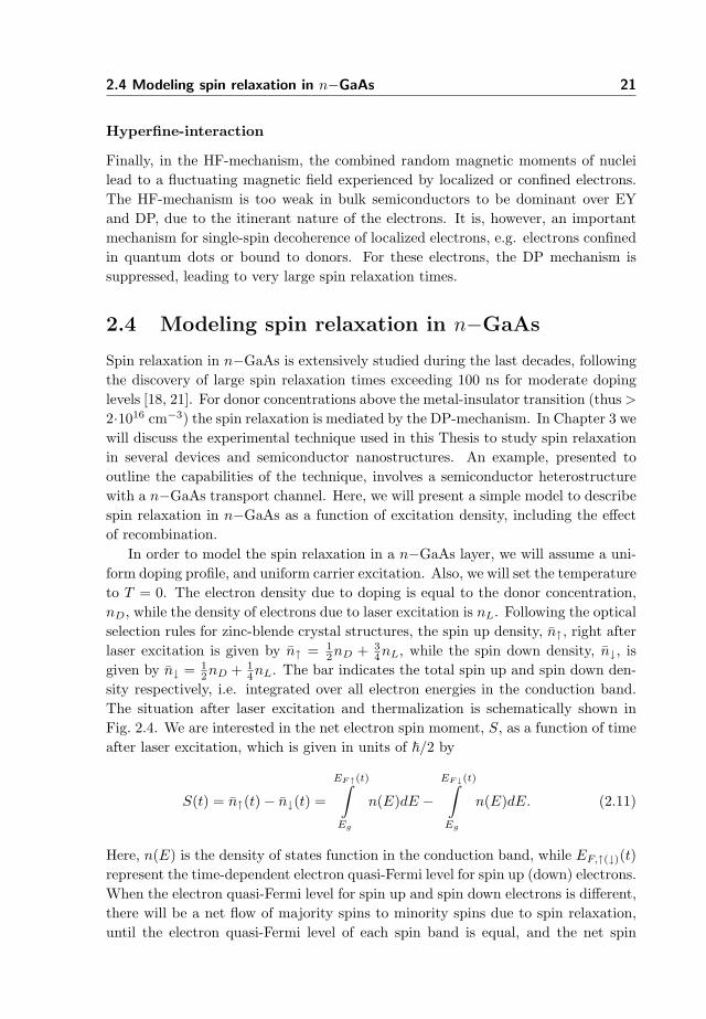
Figure 2.5: Calculated spin relaxation times τs as a function of donordensity nD. The inset shows the time traces produced by the model.Single exponential fits to these traces yield the spin relaxation time pre-sented in the main graph.
with rr the recombination parameter, and p↓ the total hole spin down density. Usingagain Eq. 2.14, we can express Eq. 2.18 in terms of the quasi-Fermi levels, and obtain(with Eg = 0)
dEF↑(t)dt
|rec = −rrEF↑(t)3
(23n0
(EF↑(t)3/2 + EF↓(t)3/2
)− nD
). (2.19)
The right-hand side of Eq. 2.19 can be added to the right-hand side of Eq. 2.17,thereby obtaining the full rate equation for the spin up density. Together withthe similar equation for the spin down density this forms a system of two coupleddifferential equations, which can be solved in order to obtain EF↑(t) and EF↓(t).Using Eq. 2.12 we obtain n↑(t) and n↓(t). Substituting these quantities in Eq. 2.11finally yields S(t), the evolution of the total spin density as a function of time. Wehave employed a numerical technique to solve the coupled differential equations, andhave calculated S(t) for several values of the input parameters nD, nL, and rr.
First, we verified that the model agrees with the paper of Dzhioev et al., whichshould be the case because the data of Dzhioev et al. serves as an input. Therefore,we calculated the spin relaxation time for several donor concentration in the lowfluence limit (nL ¿ nD). This means that we used a laser induced electron concen-tration of 1 × 1015 cm−3, much smaller than all the donor concentrations. Figure2.5 shows the calculated spin relaxation times, as well as the time traces producedby the model in the inset. Comparison with Fig. 2.4b shows that indeed the same
2.4 Modeling spin relaxation in n−GaAs 25
0 1 2 3
1016
1017
.
n n n S
n, n
, n
, S (c
m-3)
Time (ns)
rr = 0 cm3/s(a)
rr = 20 10-9 cm3/s(rec. only)(b)
0 1 2 3
Time (ns)
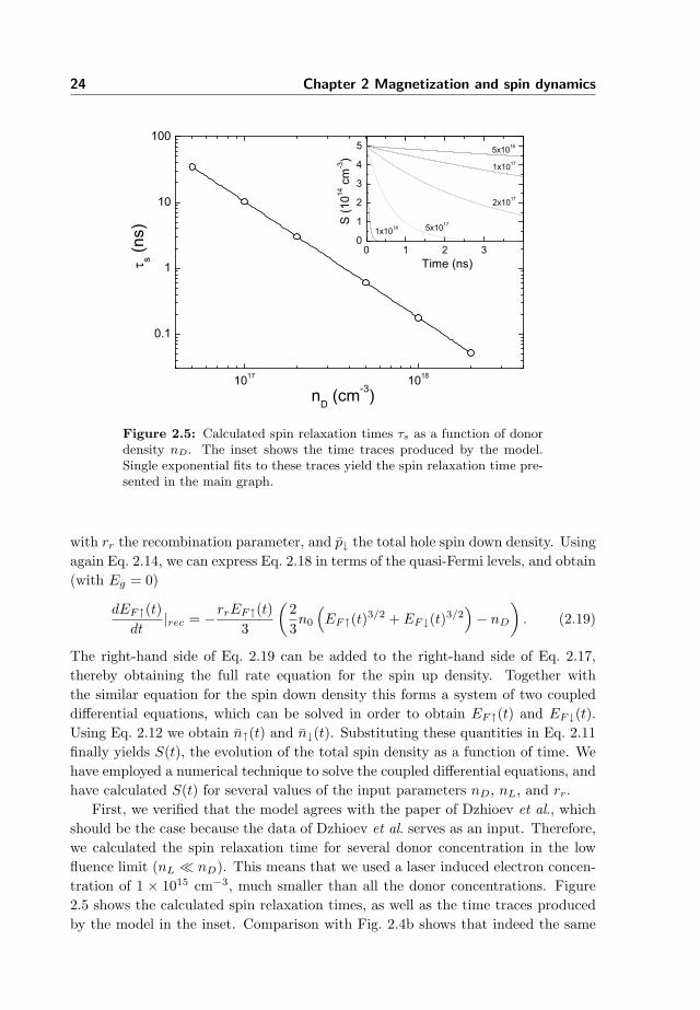
Figure 2.6: Calculated total spin S, the total carrier (n), total spin up(n↑), and total spin down (n↓) density for the case of only spin relaxation(a) and only recombination (b). The input parameters of the model arenD = 5× 1016 cm−3, nL = 3× 1017 cm−3.
dependence of τs on nD is reproduced.
A more interesting application of the model is to study the spin relaxation inthe case of high fluence (nL > nD). First, we will focus on the effect on S of (i)only spin relaxation, and (ii) only recombination. We set nD = 5 × 1016 cm−3,nL = 3 × 1017 cm−3, so n = 3.5 × 1017 cm−3 at t = 0. We choose this value fornD, because this is the donor concentration of the device discussed in Section 3.3.3.Figure 2.6 shows the total spin S, the total carrier (n), total spin up (n↑), and totalspin down (n↓) density for the two cases. If only spin relaxation is present, and norecombination, Fig. 2.6a shows that n is constant. n↑ decreases while n↓ increasesdue to spin flips, resulting in a decay of S, which can be well approximated witha single exponential decay with time constant τs = 1.13 ns. This time constant issimilar to the case of low excitation density, with nD = 3.5×1017 cm−3. Apparently,the spin relaxation time is determined by the total carrier density, and is only weaklychanged by an initial large spin up and spin down imbalance. If only recombinationis present, and no spin relaxation, Fig. 2.6b shows a non-exponential decay of thecarrier density, which follows from Eq. 2.18 because p↓ is time-dependent. Also,because at t = 0 n↑ > n↓, unequal recombination rates for spin up and spin downelectrons are observed. This leads to a net loss of spin polarization, and thus to adecrease of S.
When both spin relaxation and recombination are present, it is expected that thespin relaxation rate due to spin flips is time-dependent. This follows from the DP-
26 Chapter 2 Magnetization and spin dynamics
0 1 2 31016
1017
.. (c)(b) rr = 20 10-9 cm3/s rr = 200 10-9 cm3/s
n n n S
n, n
, n
, S (c
m-3)
Time (ns)
rr = 2 10-9 cm3/s(a) .
0 1 2 3
Time (ns)0 1 2 3
Time (ns)
Figure 2.7: Calculated total spin S, the total carrier (n), total spin up(n↑), and total spin down (n↓) density for three different recombinationparameters. The input parameters of the model are nD = 5×1016 cm−3,nL = 3× 1017 cm−3.
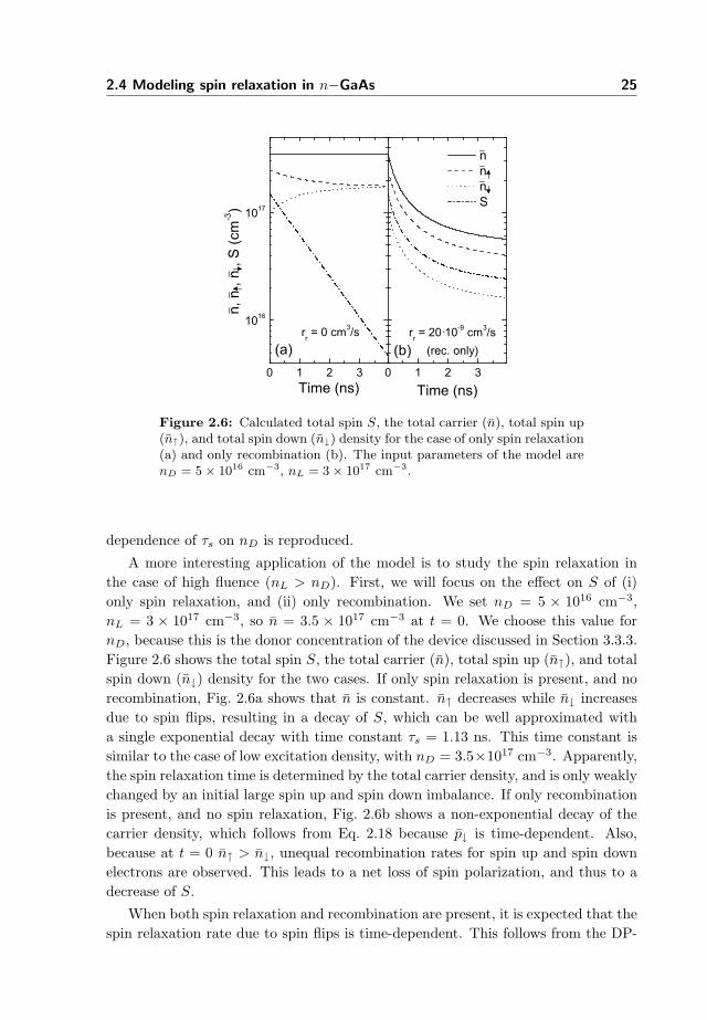
mechanism, according to which the spin flip rate depends on the spin up and spindown density. Due to recombination, these densities decrease, thereby decreasingthe spin flip rate. In Figure 2.7 we show the results of calculations (S, n, n↑, andn↓) with again nD = 5 × 1016 cm−3, and nL = 3 × 1017 cm−3, for three differentvalues for the recombination parameter rr.
We want to focus on a few aspects of these results. Firstly, the effect of therecombination parameter on n is clearly visible: the higher rr the faster the decayof n. Secondly, in Fig. 2.7a the relatively little loss of spin down electrons dueto recombination is compensated by spin flips of spin up electrons during the firstns. In (b) and (c) recombination is initially the dominant process, leading to adecrease of n↓ and a fast decrease of S. Finally, the spin polarization S after fullrecombination strongly depends on rr. With a small rr, the densities n↑, and n↓remain relatively high for several ns, leading to fast spin relaxation at these highdensities. When rr is large, the laser excited carriers recombine quickly, leaving onlya short time-interval with a high spin flip rate, and a marginal loss of S due to spinflip events. After full recombination, S is larger when rr is large, as can be seen inFig. 2.7.
The model presented above enables the calculation of the relaxation of an opti-cally induced spin polarization in n−GaAs in the moderate to high fluence regime,where the optically induced carrier density is comparable or higher than the donorconcentration. In the next Section, we will address spin precession and dephasing in
2.5 Spin precession and dephasing 27
n−GaAs, which is the result of application of a transverse external magnetic field.
2.5 Spin precession and dephasing
When a single electron is placed in a magnetic field, its energy depends on theorientation of its spin with respect to the direction of the magnetic field. Theenergy difference between spin up (parallel to the field) and spin down (anti-parallelto the field) electrons is the Zeeman-energy and is given by
∆EZ = EZ,↑ − EZ,↓ = −gµBB, (2.20)
with EZ,↑(↓) the energy of the spin up (down) electron, g the electronic g factor,µB the Bohr-magneton, and B the magnetic induction. The eigenstates of the spinpart of the electron wavefunction are ψ↑ (spin up) and ψ↓ (spin down), with respectthe quantization axis in the z direction when the magnetic field is B = (0, 0, Bz). Aspin orientated parallel to the x direction can then be represented as a superpositionof these eigenstates, according to
ψ(t) =ψ↑2
exp(− ıEZ,↑
ht
)+
ψ↓2
exp(− ıEZ,↓
ht
), (2.21)
For this spin wavefunction, the expectation value of the x−component of the spinis
Sx(t) = 〈ψ(t)∗|σx|ψ(t)〉 =~2
cos(
∆EZ
ht
), (2.22)
with σx the Pauli spin operator for the x direction. A similar analysis for the y andz direction reveals that the spin evolves according to a precessional motion aroundthe magnetic field. In the case of optical orientation in a solid, the orientation of thespin polarization is parallel to the direction of light propagation (or anti-parallel,depending on the helicity of the photons), and usually normal to the sample surface.In the presence of a transverse magnetic field, this means that the spins are createdin a coherent superposition of the spin up and spin down states with respect to thetransverse magnetic field. The whole spin density will then undergo a precessionalmotion with a frequency given by ω = ∆EZ/~. The frequency is thus proportionalto the g factor.
In solids, the g factor depends on the electron energy [22–24]. For GaAs e.g. theg factor is given by g = g0 + βE, with g0 = −0.44 and β = 6.3 eV−1. This meansthat under optical orientation in the high fluence regime, the g factor of electronspins is time-dependent due to carrier recombination, because recombination lowersthe (average) energy of the electrons. In the presence of a transverse magnetic field,and if the carrier recombination time τr is much shorter than the spin relaxationtime τs, this leads to a precession frequency that changes in time.
28 Chapter 2 Magnetization and spin dynamics
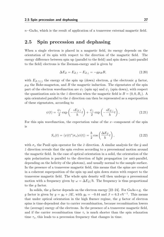
E
n(E)
EF,L
EF,L
EF,R EF,R
tr
tr
Figure 2.8: Schematic representation of the spin dependent density ofstates in the conduction band after laser excitation in n−GaAs. Theelectron quasi-Fermi levels after excitation (index L), and after recom-bination (index R), are indicated. τr represents the recombination time.
In view of the example presented in Chapter 3, we will analyze the consequencesof an energy dependent g factor in more detail. For simplicity, and in contrast to themodel of the previous paragraph, we will neglect spin relaxation due to spin flips,and simulate the recombination process by an exponentially decreasing electronquasi-Fermi level, as indicated in Fig. 2.8. Using Eq. 2.14, the electron quasi-Fermilevels of spin up and spin down after excitation are
EF,L↑ =[
32n0
(12nD +
34nL
)]2/3
, EF,L↓ =[
32n0
(12nD +
14nL
)]2/3
, (2.23)
respectively, while the electron quasi-Fermi levels after recombination (EF,R↑, andEF,R↓) can be fixed in order to have a finite remaining spin polarization. We modelthe precession of spin up and spin down electrons separately, and keep track of theprecession phase of electrons not lost in the recombination process. The precessionphase as a function of time is given by
φ(t) =
t∫
0
ω(t′)dt′ =
t∫
0
−g(E(t′))µBB
~dt′ =
t∫
0
−(g0 + βE(t′))µBB
~dt′. (2.24)
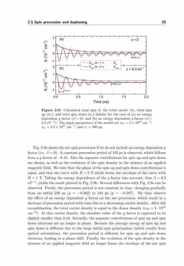
We calculate the time-dependent projection of the spin moment on the initial orien-tation direction for each energy, and integrating over the full energy range betweenEg and Eg +EF↑(↓) gives the total projection of spin up (down) electrons as a func-tion of time. The net spin projection is equal to the difference between the spin upand spin down projections. As an example, we plot in Fig. 2.9 the calculated resultfor the initial parameters nD = 5 ·1016 cm−3, nL = 2.5 ·1017 cm−3, a recombinationtime τr = 300 ps, and a magnetic field of B = 1 T. We fix the final spin polarizationafter recombination at 2.0 · 1016 cm−3, similar to the result of Fig. 2.7c.
2.5 Spin precession and dephasing 29
0.0 0.5 1.0 1.5 2.0
-1
0
1
2
-1
0
1
2
118 ps
Stotal (B = 1 T) Sup
Stotal (B = 0 T) Sdown
S (1
0-17 c
m-3)
Time (ns)
92 ps
81 ps
(b) = 6.3 eV-1
S (1
0-17 c
m-3) = 0(a)
Figure 2.9: Calculated total spin S, the total carrier (n), total spinup (n↑), and total spin down (n↓) density for the case of (a) no energydependent g factor (β = 0), and (b) an energy dependent g factor (β =6.3 eV−1). The input parameters of the model are nD = 5× 1016 cm−3,nL = 2.5× 1017 cm−3, and τr = 300 ps.
Fig. 2.9a shows the net spin precession if we do not include an energy-dependent g
factor (i.e. β = 0). A constant precession period of 162 ps is observed, which followsfrom a g factor of −0.44. Also the separate contributions for spin up and spin downare shown, as well as the evolution of the spin density in the absence of an appliedmagnetic field. We note that the phase of the spin up and spin down contributions isequal, and that the curve with B = 0 T nicely forms the envelope of the curve withB = 1 T. Taking the energy dependence of the g factor into account, thus β = 6.3eV−1, yields the result plotted in Fig. 2.9b. Several differences with Fig. 2.9a can beobserved. Firstly, the precession period is not constant in time, changing graduallyfrom an initial 236 ps (g = −0.302) to 184 ps (g = −0.387). We thus observethe effect of an energy dependent g factor on the net precession, which result in adecrease of precession period with time due to a decreasing carrier density. After fullrecombination, the total carrier density is equal to the donor density (nD = 5 · 1016
cm−3). At this carrier density, the absolute value of the g factor is expected to beslightly smaller than 0.44. Secondly, the separate contributions of spin up and spindown electrons are no longer in phase. Because the average energy of spin up andspin down is different due to the large initial spin polarization (which results fromoptical orientation), the precession period is different for spin up and spin downelectrons, leading to a phase shift. Finally, the evolution of the spin density in theabsence of an applied magnetic field no longer forms the envelope of the net spin
30 Chapter 2 Magnetization and spin dynamics
precession. For 0.15 < t < 0.85 ns, the maxima of the net spin precession are largerthan the zero field curve, whereas for t > 1 ns, the maxima are smaller than thezero field data. The former aspect results from the phase difference between spinup and spin down electrons, which enhances the net spin precession amplitude. Thelatter aspect is a result of spin dephasing due to a distribution in g factors. Theeffective spin lifetime resulting from dephasing due to a Gaussian distribution of g
factors is given by [21]
Teff =~√
2∆gµBB
. (2.25)
With a final spin polarization after recombination of 2.0 · 1016 cm−3, this meansthat the net spin precession occurs within a carrier energy width of ≈ 4.2 meV.This energy width corresponds to a ∆g of 0.026. Using this ∆g as a measure of thewidth of a Gaussian distribution, Eq. 2.25 yields a spin dephasing time of Teff = 0.6ns, which is of the same order as the decrease of the precession amplitude observedin Fig. 2.9b.
These results show that spin precession in the moderate to high fluence regimecan result in a time-dependent precession frequency due to an energy dependenceof the electron g factor. Also, a relative large energy window of spin polarizedelectrons after recombination strongly increases the dephasing of electron spins,thereby reducing the effective spin lifetime.

BIBLIOGRAPHY 31
Bibliography
[1] L. Landau and E. Lifshitz, On the theory of the dispersion of magnetic perme-ability in ferromagnetic bodies, Phys. Z. Sowjetunion 8, 153 (1953). 2.1
[2] T. L. Gilbert, A Lagrangian formulation of the gyromagnetic equation of themagnetic field, Phys. Rev. 100, 1243 (1955). 2.1
[3] T. L. Gilbert, A phenomenological theory of damping in ferromagnetic metals,IEEE Trans. Magn. 40, 3443-3449 (2004). 2.1, 2.1
[4] B. A. Kalinikos, and A. N. Slavin, Theory of dipole-exchange spin wave spectrumfor ferromagnetic films with mixed exchange boundary conditions, J. Phys. C:Solid State Phys. 19, 7013-7033 (1986) 2.1
[5] R. W. Damon, J. R. Eshbach, Magnetostatic modes of a ferromagnet slab, J.Phys. Chem. Solids 19, 308-320 (1961). 2.1
[6] S. O. Demokritov, Dynamic eigen-modes in magnetic stripes and dots, J. Phys.:Condens. Matter 15,S2575-S2598 (2003). 2.1
[7] C. Mathieu, J. Jorzick, A. Frank, S. O. Demokritov, B. Hillebrands, B. Barten-lian, C. Chappert, D. Decanini, F. Rousseaux, and E. Cambril, Lateral Quan-tization of Spin Waves in Micron Size Magnetic Wires, Phys. Rev. Lett. 813968-3971 (1998). 2.1
[8] J. Jorzick, S. O. Demokritov, B. Hillebrands, M. Bailleul, C. Fermon, K. Y.Guslienko, A. N. Slavin, D. V. Berkov, and N. L. Gorn, Spin Wave Wellsin Nonellipsoidal Micrometer Size Magnetic Elements, Phys. Rev. Lett. 88,047204 (2002). 2.1
[9] J. P. Park, P. Eames, D. M. Engebretson, J. Berezovksy, and P. A. Crowell,Spatially Resolved Dynamics of Localized Spin-Wave Modes in FerromagneticWires, Phys. Rev. Lett. 89, 277201 (2002). 2.1
[10] Optical Orientation (Modern Problems in Condensed Matter Sciences, Vol. 8),edited by F. Meier, and B. P. Zachachrenya (North-Holland, Amsterdam, 1984).2.2, 2.3
[11] M. R. Brozel, and G. E. Stillman, Properties of Gallium Arsenide (3rd Edition),(London: INSPEC, 1996). 2.2
[12] P. H. Song, and K. W. Kim, Spin relaxation of conduction electrons in bulkIII-V semiconductors, Phys. Rev. B 66, 035207 (2002). 2.3
[13] R. J. Elliott, Theory of the effect of spin-orbit coupling on magnetic resonancein some semiconductors, Phys. Rev. 96, 266-279 (1954). 2.3
32 Chapter 2 Magnetization and spin dynamics
[14] Y. Yafet, in Solid State Physics, Vol. 14, edited by F. Seitz and D. Turnbull(Academic, New York, 1963), p. 2. 2.3
[15] J.-N. Chazalviel, Spin relaxation of conduction electrons in n-type indium an-timonide at low temperature, Phys. Rev. B 11, 1555-1562 (1975). 2.3
[16] A. G. Aronov, G. E. Pikus, and A. N. Titkov, Spin relaxation of conductionelectrons in p-type III-V compounds, Zh. Eksp. Teor. Fiz. 84, 1170-1184 (1983)[Sov. Phys. JETP 57, 680-687 (1983)]. 2.3, 2.3, 2.3
[17] M. I. D’yakonov, and V. I. Perel’, Spin orientation of electrons associated withthe interband absorption of light in semiconductors, Zh. Eksp. Teor. Fiz. 60,1954-1965 (1971) [Sov. Phys. JETP 33, 1053-1059 (1971)]. 2.3
[18] R. I. Dzhioev, K. V. Kavokin, V. L. Korenev, M. V. Lazarev, B. Y. Meltser,M. N. Stepanova, B. P. Zakharchenya, D. Gammon, and D. S. Katzer, Low-temperature spin relaxation in n-type GaAs, Phys. Rev. B 66, 245204 (2002).2.3, 2.4, 2.4, 2.4
[19] G. L. Bir, A. G. Aronov, and G. E. Pikus, Spin relaxation of electrons due toscattering by holes, Zh. Eksp. Teor. Fiz. 69, 1382-1397 (1975) [Sov. Phys. JETP42, 705-712 (1976)]. 2.3
[20] K. Zerrouati, F. Fabre, G. Bacquet, J. B. J. Frandon, G. Lampel, and D. Paget,Spin-lattice relaxation in p-type gallium arsenide single crystals, Phys. Rev. B37, 1334-1341 (1988). 2.3
[21] J. M. Kikkawa, and D. D. Awschalom, Resonant spin amplification in n-typeGaAs, Phys. Rev. Lett. 80, 4313- 4316 (1998). 2.4, 2.5
[22] M. A. Hopkins, R. J. Nicholas, P. Pfeffer, W. Zawadzki, D. Gauthier, J.C. Portal, and M. A. DiForte-Poisson, A study of the conduction band non-parobolicity, anisotropy, and spin splitting in GaAs and InP, Semicond. Sci.Technol. 2, 568 (1987). 2.5
[23] H. Mayer, and U. Rossler, Spin splitting and anisotropy of cyclotron resonancein the conduction band of GaAs, Phys. Rev. B 44, 9048 (1991).
[24] M. Oestreich, S. Hallstein, A. P. Heberle, K. Eberl, E. Bauser, and W. W.Ruhle, Temperature and density dependence of the electron Lande g factor insemiconductors, Phys. Rev. B 53, 7911 (1996). 2.5
Chapter 3
Magneto-optical techniques
This Chapter discusses the experimental tools, which are used throughout this The-
sis to study magnetization and spin dynamics in spintronic devices and semicon-
ductor nanostructures. These experimental tools all employ magneto-optical tech-
niques and are referred to as: Magneto-optical Kerr-effect (MOKE), Time-resolved
magneto-optical Kerr-effect (TR-MOKE) and Time-resolved magnetization modu-
lation spectroscopy (TiMMS). This Chapter discusses in detail the magneto-optical
techniques, and the experimental implementation. Also, unpublished experimental
results obtained with these techniques will be presented in order to demonstrate the
power of these techniques. Finally, this Chapter contains simulation results which
facilitate the interpretation of data obtained on complicated multilayer systems.1
1Part of Section 1.5 of this Chapter is published as G. Malinowski, F. Dalla Longa, J. H. H.Rietjens, P. V. Paluskar, R. Huijink, H. J. M Swagten, and B. Koopmans, Control of speed andefficiency of ultrafast demagnetization by direct transfer of spin angular momentum, Nat. Phys.4, 855 (2008).
33
34 Chapter 3 Magneto-optical techniques
3.1 MOKE
In this Thesis, most experimental techniques used to probe magnetism and spinrelated processes rely on the magneto-optical Kerr-effect (MOKE). This effect isused to determine static magnetic properties of magnetic multilayers, such as co-ercivity, remanence, and switching behavior. Also, time-resolved techniques suchas TR-MOKE and TiMMS, to be discussed in following sections, probe the dy-namic behavior of the magnetization, and an optically induced spin distributionrespectively, via MOKE. In this Section, we will give a basic description of MOKE,present an experimental setup for measuring static magnetic properties, and dis-cuss an illustrative example. Also, we will outline a procedure for calculating theMOKE originating from an arbitrary system of magnetic multilayers, and presentan important application of this procedure.
3.1.1 Basics of MOKE
The basis of the Kerr-effect is a change in polarization state of incident light uponreflection from a medium with an unequal population of spin up and spin down elec-trons, such as a ferromagnetic material or a semiconductor with a non-equilibriumspin distribution. Microscopically, the Kerr-effect results from spin-orbit coupling,the coupling of spin angular momentum with the orbital angular momentum. Thedipole selection rules are governed by the orbital angular momentum. Spin-orbitcoupling induces a correlation between the orbital and spin angular momenta, whichallows one to optically probe the spin system via the dipole selection rules. However,because the orbital momentum in 3d transition metals is largely quenched by crystalfield effects, the Kerr-effect is generally small. For a detailed theoretical description,the reader is referred to Ref. [1].
In a phenomenological picture, the response of a medium to an incident electro-magnetic wave is given by the dielectric tensor ~~ε, via ~D = ~~ε ~E. Here, ~E is the electricfield, and ~D is the electric displacement. In general, for an isotropic medium itfollows from symmetry arguments that the non-diagonal elements εij vanish, andthe diagonal elements εii are equal, so that ~~ε reduces to a scaler. However, inanisotropic media the non-diagonal elements of ~~ε do not necessarily vanish. In thespecial case of an isotropic medium with a finite magnetization ~M = (mx,my,mz),~~ε is given by
~~ε =
εxx εxy(mz) εxz(my)−εxy(mz) εxx εyz(mx)−εxz(my) −εyz(mx) εxx
.
. (3.1)
To first order, the diagonal elements are independent of ~M , and the off-diagonalelements εij depend linearly on ~M in the direction i× j. Also, εij( ~M) = −εij(− ~M).The off-diagonal elements εij are sometimes expressed as εij = ıQmi×j · εxx, withQ = ıεxy/εxx the magneto-optical Voigt parameter, or simply the magneto-optical
3.1 MOKE 35
constant. Q is a complex parameter, and is a measure for the magnitude of the Kerr-effect. When ~M = (0, 0,mz), Eq. 3.1 can be diagonalized by changing to cylindricalcoordinates (i.e. c− = 1/
√2(x− ıy), c+ = 1/
√2(x + ıy), and cz = z) obtaining
~~ε =
εxx − ıεxy(mz) 0 00 εxx + ıεxy(mz) 00 0 εxx
,
. (3.2)
From this, we see that the eigenmodes of propagating electromagnetic waves inmagnetic media are left- and right-circularly polarized light, and that their cor-responding dielectric (complex) tensor elements ε−− and ε++ (and thereby theircomplex indices of refraction, n− and n+) are different. A linearly polarized wave,which can be viewed as the sum of left- and right-circularly polarized waves, will thusexperience a change in polarization state after reflection from a magnetic medium.This change manifests itself in a rotation of the polarization axis, and an increasein ellipticity, and is schematically shown in Fig. 3.1a. The complex Kerr-rotationcan then be defined as
ΘK = θK + ıεK =r+ − r−
1/2(r+ + r−), (3.3)
with r+ and r− the reflection coefficients for left- and right circularly polarized light.For the case of normal incidence, Eq. 3.3 can be expressed in terms of the dielectrictensor elements as
ΘK =2(n+ − n−)(n+n− − 1)
=2(ε++ − ε−−)
(√ε++ε−− − 1)(√ε++ +√ε−−)
=ıεxy
(εxx − 1)√
εxx. (3.4)
When using the Jones-formalism to describe the polarization state of light beforeand after reflection from a sample, the components of the Jones-vector represent theelectric field perpendicular (s) and parallel (p) to the plane of incidence [2]. Thesample is represented by a Jones-matrix of the form
(rss rsp
rps rpp
), (3.5)
and the complex Kerr-rotation can be expressed as ΘsK = rps/rss and Θp
K = rsp/rpp
for the case of incident s− and p−polarized light, respectively. We note that threetypes of Kerr-effect can be distinguished, depending on the relative orientation of themagnetization with respect to the plane of incidence, and the sample surface: polar,longitudinal, and transversal. The geometries of these three types are sketched inFig. 3.1b. The magnitude of the Kerr-effect is different for each geometry, and de-pends on the angle of incidence of the probing light. In general, the polar geometrygives rise to the largest Kerr-effect. At angles of incidence close to 60◦, the longi-tudinal Kerr-effect is maximal, with values close to the polar Kerr-effect at normalincidence. The transversal Kerr-effect is generally an order of magnitude smallerthan the other two. We note that in this Thesis, we will employ only the polargeometry, that is, the experiments are sensitive only to out-of-plane magnetization(or to a density of spins aligned normal to the sample surface).
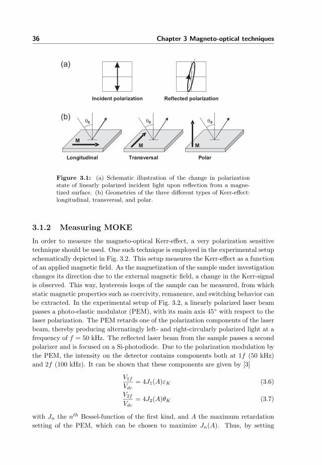
36 Chapter 3 Magneto-optical techniques
Longitudinal Transversal Polar
M
M M
q0 q0 q0
(a)
(b)
Incident polarization Reflected polarization
Figure 3.1: (a) Schematic illustration of the change in polarizationstate of linearly polarized incident light upon reflection from a magne-tized surface. (b) Geometries of the three different types of Kerr-effect:longitudinal, transversal, and polar.
3.1.2 Measuring MOKE
In order to measure the magneto-optical Kerr-effect, a very polarization sensitivetechnique should be used. One such technique is employed in the experimental setupschematically depicted in Fig. 3.2. This setup measures the Kerr-effect as a functionof an applied magnetic field. As the magnetization of the sample under investigationchanges its direction due to the external magnetic field, a change in the Kerr-signalis observed. This way, hysteresis loops of the sample can be measured, from whichstatic magnetic properties such as coercivity, remanence, and switching behavior canbe extracted. In the experimental setup of Fig. 3.2, a linearly polarized laser beampasses a photo-elastic modulator (PEM), with its main axis 45◦ with respect to thelaser polarization. The PEM retards one of the polarization components of the laserbeam, thereby producing alternatingly left- and right-circularly polarized light at afrequency of f = 50 kHz. The reflected laser beam from the sample passes a secondpolarizer and is focused on a Si-photodiode. Due to the polarization modulation bythe PEM, the intensity on the detector contains components both at 1f (50 kHz)and 2f (100 kHz). It can be shown that these components are given by [3]
V1f
Vdc= 4J1(A)εK (3.6)
V2f
Vdc= 4J2(A)θK (3.7)
with Jn the nth Bessel-function of the first kind, and A the maximum retardationsetting of the PEM, which can be chosen to maximize Jn(A). Thus, by setting
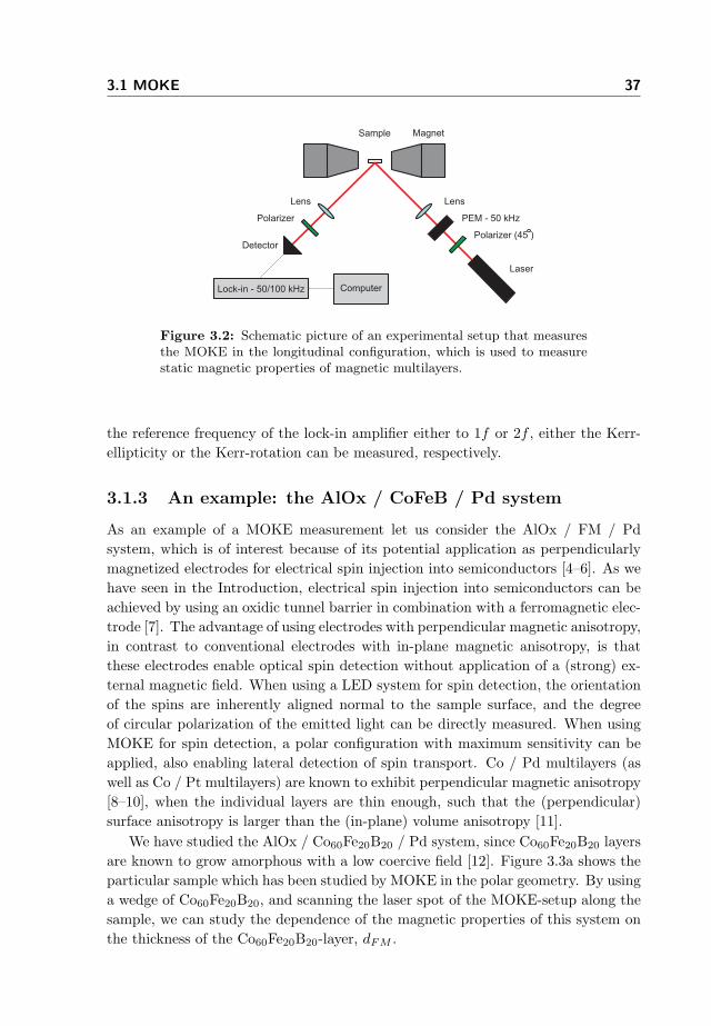
3.1 MOKE 37
Polarizer
Polarizer (45 )Detector
MagnetSample
Laser
PEM - 50 kHz
Lens
ComputerLock-in - 50/100 kHz
Lens
Figure 3.2: Schematic picture of an experimental setup that measuresthe MOKE in the longitudinal configuration, which is used to measurestatic magnetic properties of magnetic multilayers.
the reference frequency of the lock-in amplifier either to 1f or 2f , either the Kerr-ellipticity or the Kerr-rotation can be measured, respectively.
3.1.3 An example: the AlOx / CoFeB / Pd system
As an example of a MOKE measurement let us consider the AlOx / FM / Pdsystem, which is of interest because of its potential application as perpendicularlymagnetized electrodes for electrical spin injection into semiconductors [4–6]. As wehave seen in the Introduction, electrical spin injection into semiconductors can beachieved by using an oxidic tunnel barrier in combination with a ferromagnetic elec-trode [7]. The advantage of using electrodes with perpendicular magnetic anisotropy,in contrast to conventional electrodes with in-plane magnetic anisotropy, is thatthese electrodes enable optical spin detection without application of a (strong) ex-ternal magnetic field. When using a LED system for spin detection, the orientationof the spins are inherently aligned normal to the sample surface, and the degreeof circular polarization of the emitted light can be directly measured. When usingMOKE for spin detection, a polar configuration with maximum sensitivity can beapplied, also enabling lateral detection of spin transport. Co / Pd multilayers (aswell as Co / Pt multilayers) are known to exhibit perpendicular magnetic anisotropy[8–10], when the individual layers are thin enough, such that the (perpendicular)surface anisotropy is larger than the (in-plane) volume anisotropy [11].
We have studied the AlOx / Co60Fe20B20 / Pd system, since Co60Fe20B20 layersare known to grow amorphous with a low coercive field [12]. Figure 3.3a shows theparticular sample which has been studied by MOKE in the polar geometry. By usinga wedge of Co60Fe20B20, and scanning the laser spot of the MOKE-setup along thesample, we can study the dependence of the magnetic properties of this system onthe thickness of the Co60Fe20B20-layer, dFM .
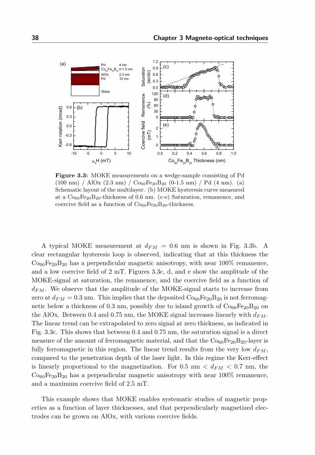
38 Chapter 3 Magneto-optical techniques
0.0 0.2 0.4 0.6 0.8 1.0
0
1
2
-10 -5 0 5 10
-0.6
-0.3
0.0
0.3
0.6
Coe
rciv
e fie
ld(m
T)
Co60
Fe20
B20
Thickness (nm)
0306090
120
Rem
anen
ce(%
)
0.0
0.3
0.6
0.9
1.2
Satu
ratio
n(a
c/dc
)
(a)
(e)
(d)
(c)
0H (mT)
Ker
r rot
atio
n (m
rad) (b)
Pd 4 nmCo
60Fe
20B
200-1.5 nm
AlOx 2.3 nmPd 10 nm
Glass
Figure 3.3: MOKE measurements on a wedge-sample consisting of Pd(100 nm) / AlOx (2.3 nm) / Co60Fe20B20 (0-1.5 nm) / Pd (4 nm). (a)Schematic layout of the multilayer. (b) MOKE hysteresis curve measuredat a Co60Fe20B20-thickness of 0.6 nm. (c-e) Saturation, remanence, andcoercive field as a function of Co60Fe20B20-thickness.
A typical MOKE measurement at dFM = 0.6 nm is shown in Fig. 3.3b. Aclear rectangular hysteresis loop is observed, indicating that at this thickness theCo60Fe20B20 has a perpendicular magnetic anisotropy, with near 100% remanence,and a low coercive field of 2 mT. Figures 3.3c, d, and e show the amplitude of theMOKE-signal at saturation, the remanence, and the coercive field as a function ofdFM . We observe that the amplitude of the MOKE-signal starts to increase fromzero at dFM = 0.3 nm. This implies that the deposited Co60Fe20B20 is not ferromag-netic below a thickness of 0.3 nm, possibly due to island growth of Co60Fe20B20 onthe AlOx. Between 0.4 and 0.75 nm, the MOKE signal increases linearly with dFM .The linear trend can be extrapolated to zero signal at zero thickness, as indicated inFig. 3.3c. This shows that between 0.4 and 0.75 nm, the saturation signal is a directmeasure of the amount of ferromagnetic material, and that the Co60Fe20B20-layer isfully ferromagnetic in this region. The linear trend results from the very low dFM ,compared to the penetration depth of the laser light. In this regime the Kerr-effectis linearly proportional to the magnetization. For 0.5 nm < dFM < 0.7 nm, theCo60Fe20B20 has a perpendicular magnetic anisotropy with near 100% remanence,and a maximum coercive field of 2.5 mT.
This example shows that MOKE enables systematic studies of magnetic prop-erties as a function of layer thicknesses, and that perpendicularly magnetized elec-trodes can be grown on AlOx, with various coercive fields.
3.1 MOKE 39
3.1.4 MOKE in a general multilayer system
In the previous example we have seen that the Kerr-effect was linearly proportionalto the total magnetization of the system, as a result of the very thin layers used. Inthe case of thicker layers or multilayer systems, however, this linear proportionalityis no longer valid. In general, the magnitude of the Kerr-effect depends on thewavelength, angle of incidence, and initial polarization of the light wave, and on thedirection of the magnetization with respect to the plane of incidence. Also, it isdependent on the complex refractive index, and complex magneto-optical constantsof each layer. In case of a multilayer system with magnetic and non-magnetic layers,also multiple internal reflections of the light wave have to be taken into account. Auseful approach for tackling the general problem of an arbitrary magnetic multilayeris given by Zak et al. [13, 14]. This approach is based on the so-called mediumboundary matrix A, and medium propagation matrix D, which we shall brieflyexplain here.
The boundary matrix A facilitates the problem of fulfilling the boundary condi-tions of the electromagnetic field at each interface. Consider two media separatedby the x− y plane as shown in Fig. 3.4. An electro-magnetic wave ~E
(i)1 is incident
on medium 1 at an angle θ with the z axis, and has components E(i)1s (perpendic-
ular) and E(i)1p (parallel) to the plane of incidence. Part of the wave is reflected at
the interface, denoted by ~E(r)1 , and a part is transmitted, denoted by ~E
(i)2 . At the
boundary (z = 0), the components of the electric field, ~E, and magnetic field, ~H,parallel to the boundary are continuous. Defining the vector ~Fm for medium m as
~Fm =
Em,x
Em,y
Hm,x
Hm,y
, (3.8)
the boundary conditions can be expressed as ~F1 = ~F2. In order to express theboundary conditions in terms of the electro-magnetic wave components En
m, thevector ~P is defined as
~Pm =
E(i)m,s
E(i)m,p
E(r)m,s
E(r)m,p
. (3.9)
The medium boundary matrix A connects ~F to ~P via ~F = A~P , and the boundaryconditions can be expressed as
A1~P1 = A2
~P2. (3.10)
This is a set of four linear equations with the unknowns E(r)1s , E
(r)1p , E
(i)2s , and E
(i)2p ,
which can be solved once the medium boundary matrix A is known. In case of

40 Chapter 3 Magneto-optical techniques
medium 1
medium 2
E1
(i)
E1s
(i)
E1
(r)
E2
(r)E2
(i)
E1p
(i)
y
z
qx
Figure 3.4: Two media separated by the x− y plane. Light is incident(i) from medium 1, and at the interface between medium 1 and 2 it ispartly reflected (r) back to medium 1, and partly transmitted to medium2. The angle of incidence is θ, Es and Ep are the electric field componentsperpendicular (s), and parallel (p), to the plane of incidence (y−z plane).
more than one boundary (as in multilayers systems) the propagation of the electro-magnetic wave inside the medium has to be taken into account. This propagationis expressed by the medium propagation matrix Dm. It connects ~P t
m at the topinterface to ~P b
m at the bottom interface via
~P tm = Dm(d)~P b
m, (3.11)
with d the thickness of medium m. Using the matrices Am and Dm, we can nowrelate the vector ~Pi of the initial medium to the vector ~Pf of the final medium byrepeatedly using Eqs. 3.10 and 3.11:
~Pi = A−1i A2
~P t2 = A−1
i A2D2~P b2 = A−1
i (A2D2A−12 )A3
~P t3
= A−1i
l∏m=1
(AmDmA−1m )Af
~Pf = M~Pf . (3.12)
Here, the matrix M can be viewed as the full reflection-transmission matrix of theproblem. In order to calculate M and solve Eq. 3.12, the matrices Am and Dm needto be calculated for every layer. Analytical expressions exist for these matrices forarbitrary direction of the magnetization. However, we will not write down the fullform here, and refer the interested reader to the papers of Zak et al. [13, 14]. We notethat Am and Dm depend on the photon energy, the angle of incidence on layer m,and on layer specific parameters, such as the orientation of the magnetization, the
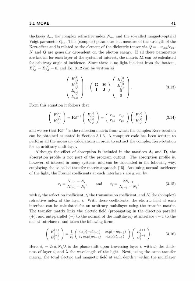
3.1 MOKE 41
thickness dm, the complex refractive index Nm, and the so-called magneto-opticalVoigt parameter Qm. This (complex) parameter is a measure of the strength of theKerr-effect and is related to the element of the dielectric tensor via Q = −ıεxy/εxx.N and Q are generally dependent on the photon energy. If all these parametersare known for each layer of the system of interest, the matrix M can be calculatedfor arbitrary angle of incidence. Since there is no light incident from the bottom,E
(r)f,s = E
(r)f,p = 0, and Eq. 3.12 can be written as
E(i)i,s
E(i)i,p
E(r)i,s
E(r)i,p
=
(G HI J
)
E(i)f,s
E(i)f,p
00
. (3.13)
From this equation it follows that(
E(r)i,s
E(r)i,p
)= IG−1
(E
(i)i,s
E(i)i,p
)=
(rss rsp
rps rpp
) (E
(i)i,s
E(i)i,p
). (3.14)
and we see that IG−1 is the reflection matrix from which the complex Kerr-rotationcan be obtained as stated in Section 3.1.3. A computer code has been written toperform all the necessary calculations in order to extract the complex Kerr-rotationfor an arbitrary multilayer.
Although the effect of absorption is included in the matrices A, and D, theabsorption profile is not part of the program output. The absorption profile is,however, of interest in many systems, and can be calculated in the following way,employing the so-called transfer matrix approach [15]. Assuming normal incidenceof the light, the Fresnel coefficients at each interface i are given by
ri =Ni−1 −Ni
Ni−1 −Ni, and ti =
2Ni−1
Ni−1 −Ni, (3.15)
with ri the reflection coefficient, ti the transmission coefficient, and Ni the (complex)refractive index of the layer i. With these coefficients, the electric field at eachinterface can be calculated for an arbitrary multilayer using the transfer matrix.The transfer matrix links the electric field (propagating in the direction parallel(+), and anti-parallel (−) to the normal of the multilayer) at interface i− 1 to theone at interface i, and takes the following form:
(E
(+)i−1
E(−)i−1
)=
1ti
(exp(−ıδi−1) exp(−ıδi−1)ri exp(ıδi−1) exp(ıδi−1)
) (E
(+)i
E(−)i
). (3.16)
Here, δi = 2πdiNi/λ is the phase-shift upon traversing layer i, with di the thick-ness of layer i, and λ the wavelength of the light. Next, using the same transfermatrix, the total electric and magnetic field at each depth z within the multilayer
42 Chapter 3 Magneto-optical techniques
is evaluated, from which the Poynting vector (S = E∗H ∝ E2) can be obtained.Finally, differentiating the Poynting vector with respect to z gives the absorptionprofile A(z).
As an example of the application of the above theory to a physical system, we willpresent an important case study regarding Co/Pt multilayers in the next section.
3.1.5 A case study: Co/Pt multilayers
Co/Pt multilayers are a useful system from magnetic point of view, since thesemultilayers exhibit out-of-plane magnetization [10], as we have seen in Section 3.1.2.More importantly, a system consisting of two blocks of Co/Pt multilayers, separatedby a non-magnetic spacer, can be used to study spin angular momentum transferbetween these two multilayer blocks on a sub-picosecond time-scale by performinglaser-induced demagnetization experiments [3]. Here, we will not discuss the detailsof the experiment, and refer the interested reader to Ref. [16]. However, as in theseexperiments the absorption of a laser pulse is used to heat the system, and MOKEis used to study the demagnetization of both multilayer blocks, it is important toknow how much of the laser light is absorbed in each block, and what information ofeach block is contained in the Kerr-rotation or Kerr-ellipticity. Therefore, we haveapplied the methods of the previous section in order to calculate the absorptionprofile of the system, and the complex Kerr-rotation and -ellipticity in the polargeometry.
Before doing so, we like to point out that for very thin layers, the absorptionshould scale the same way as the Kerr-effect with increasing depth z in the mul-tilayer. Due to a finite complex part of the refractive index, k (also called extinc-tion coefficient), the amplitude of the electromagnetic (EM) wave will decrease asexp(−2πkz/λ) while propagating in the medium in the direction z. The Kerr-effectis proportional to the electric field, and in order to measure the Kerr-effect, the lighthas to travel backwards through the medium. The magnitude of the Kerr-effect orig-inating from depth z scales thus as exp(−4πkz/λ). The absorption is proportionalthe intensity of the EM wave (thus to the electric field squared), and decreases alsoas exp(−4πkz/λ) with increasing z. The absorption thus scales the same way as theKerr-effect, and therefore one expects that the ratio of absorption in the top andbottom blocks is equal to the ratio of the Kerr-effect in the top and bottom blocks.
Let us now turn to the actual calculation. We consider the following system: 10Pt / [0.4 Co / 0.7 Pt]4 / 0.4 Co / t S / 0.4 Co / [0.7 Pt / 0.4 Co]4 / 2 Pt (unitsin nanometer), with S being either Ru or NiO of thickness t. First, we focus on theabsorption profile, and the ratio of total absorption in each Co/Pt-block. In orderto calculate the absorption profile of these samples, we used the transfer matrixapproach as explained in the previous Section. We used literature values for thecomplex refractive indices N of each layer: NPt, NRu, and NSi are taken from [17],NSiOx is taken from [18]. The CoPt multilayer is treated as a single entity with the

3.1 MOKE 43
0 5 10 15 200
2
4
6
RuCo/PtCo/PtPt
Abs
orpt
ion
(% n
m-1)
Depth (nm)
Pt
Figure 3.5: Calculated absorption profile for a sample compositionof SiOx 3 / Pt 10 / CoPt 4.8 / Ru 0.4 / CoPt 4.8 / Pt 2 (units innanometer). Absorption is calculated as a fraction of the transmittedlight through the top interface, and with a wavelength of λ = 785.0 nm.
complex refractive index taken from [19].
The absorption profile of the Co/Pt-system is shown in Fig. 3.5, for the casewith S = Ru, t = 0.4 nm, and λ = 785.0 nm, which is the laser wavelength usedin the experiment. The much larger absorption coefficient of Ru with respect toboth Pt and CoPt clearly shows up in Fig. 3.5. Integrating the absorption-profilefor the two CoPt-blocks, yields the total absorption in each CoPt-block (ARu
top, andARu
bottom). From Fig. 3.5 we find that the ratio of the absorption in the top andbottom CoPt-block is ARu
top/ARubottom = 1.39 (ARu
top = 58.2% and ARubottom = 41.8%).
The calculation of the Kerr-rotation and -ellipticity originating from each of thetwo CoPt-blocks is performed using the model of Zak et al. [14], as explained in theprevious Section. By artificially setting the magneto-optic Voigt parameter for oneof the two CoPt-blocks (obtained from ref. [19]) to zero, we can calculate the Kerr-effect for each block separately. We have performed the calculation for both a Ru aswell as a NiO spacer, for various spacer thicknesses, and with λ = 785.0 nm. Figure3.6 shows the result of this calculation. We will refer to the Kerr-rotation (ellipticity)originating from the top Co/Pt-block with NiO spacer as θNiO
top (εNiOtop ), and use a
similar notation for the bottom Co/Pt-block and Ru spacer. Let us first focus onthe Kerr-rotation data. For both NiO and Ru spacers, we see that θtop is larger thanθbottom. For the NiO spacer, θNiO
top increases slowly with increasing thickness, mostlikely due to multiple reflections between the two Co/Pt-blocks, which contributionsto the total Kerr-rotation increase with increasing spacer thickness. θNiO
bottom remainsfairly constant, because of the transparency of the NiO spacer. For the Ru spacer,the situation is different. θRu
top remains fairly constant is this case, which can beexplained by the strong attenuation of the multiple reflections between the Co/Pt-
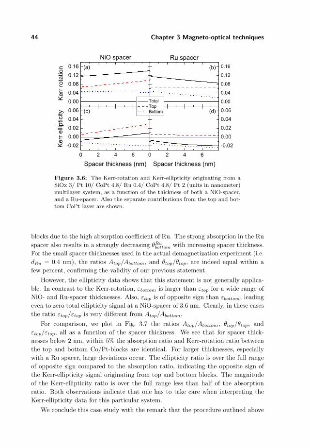
44 Chapter 3 Magneto-optical techniques
0.000.040.080.120.16
(d)(c)
(b)
K
err r
otat
ion (a)
0.00
0.04
0.08
0.12
0.16
0 2 4 6
-0.020.000.020.040.06
Ker
r elli
ptic
ity
Spacer thickness (nm)0 2 4 6
-0.020.000.020.040.06
Total Top Bottom
Ru spacer
Spacer thickness (nm)
NiO spacer
Figure 3.6: The Kerr-rotation and Kerr-ellipticity originating from aSiOx 3/ Pt 10/ CoPt 4.8/ Ru 0.4/ CoPt 4.8/ Pt 2 (units in nanometer)multilayer system, as a function of the thickness of both a NiO-spacer,and a Ru-spacer. Also the separate contributions from the top and bot-tom CoPt layer are shown.
blocks due to the high absorption coefficient of Ru. The strong absorption in the Ruspacer also results in a strongly decreasing θRu
bottom with increasing spacer thickness.For the small spacer thicknesses used in the actual demagnetization experiment (i.e.dRu = 0.4 nm), the ratios Atop/Abottom, and θtop/θtop, are indeed equal within afew percent, confirming the validity of our previous statement.
However, the ellipticity data shows that this statement is not generally applica-ble. In contrast to the Kerr-rotation, εbottom is larger than εtop for a wide range ofNiO- and Ru-spacer thicknesses. Also, εtop is of opposite sign than εbottom, leadingeven to zero total ellipticity signal at a NiO-spacer of 3.6 nm. Clearly, in these casesthe ratio εtop/εtop is very different from Atop/Abottom.
For comparison, we plot in Fig. 3.7 the ratios Atop/Abottom, θtop/θtop, andεtop/εtop, all as a function of the spacer thickness. We see that for spacer thick-nesses below 2 nm, within 5% the absorption ratio and Kerr-rotation ratio betweenthe top and bottom Co/Pt-blocks are identical. For larger thicknesses, especiallywith a Ru spacer, large deviations occur. The ellipticity ratio is over the full rangeof opposite sign compared to the absorption ratio, indicating the opposite sign ofthe Kerr-ellipticity signal originating from top and bottom blocks. The magnitudeof the Kerr-ellipticity ratio is over the full range less than half of the absorptionratio. Both observations indicate that one has to take care when interpreting theKerr-ellipticity data for this particular system.
We conclude this case study with the remark that the procedure outlined above
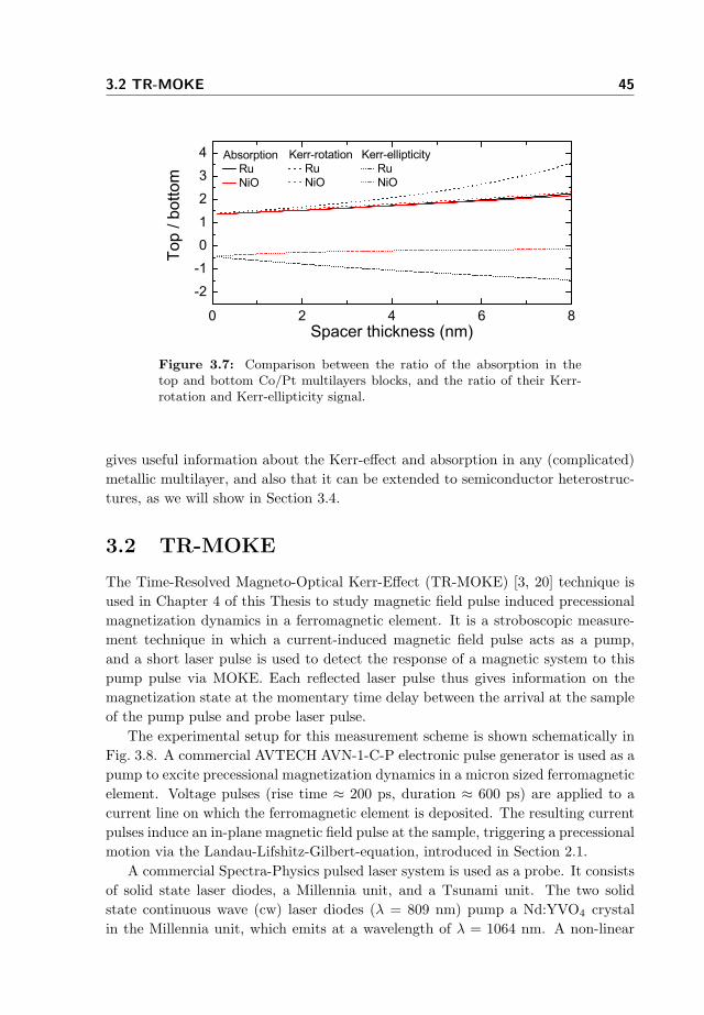
3.2 TR-MOKE 45
0 2 4 6 8
-2
-1
0
1
2
3
4 Kerr-ellipticity Ru NiO
Kerr-rotation Ru NiO
Absorption Ru NiO
Top
/ bot
tom
Spacer thickness (nm)
Figure 3.7: Comparison between the ratio of the absorption in thetop and bottom Co/Pt multilayers blocks, and the ratio of their Kerr-rotation and Kerr-ellipticity signal.
gives useful information about the Kerr-effect and absorption in any (complicated)metallic multilayer, and also that it can be extended to semiconductor heterostruc-tures, as we will show in Section 3.4.
3.2 TR-MOKE
The Time-Resolved Magneto-Optical Kerr-Effect (TR-MOKE) [3, 20] technique isused in Chapter 4 of this Thesis to study magnetic field pulse induced precessionalmagnetization dynamics in a ferromagnetic element. It is a stroboscopic measure-ment technique in which a current-induced magnetic field pulse acts as a pump,and a short laser pulse is used to detect the response of a magnetic system to thispump pulse via MOKE. Each reflected laser pulse thus gives information on themagnetization state at the momentary time delay between the arrival at the sampleof the pump pulse and probe laser pulse.
The experimental setup for this measurement scheme is shown schematically inFig. 3.8. A commercial AVTECH AVN-1-C-P electronic pulse generator is used as apump to excite precessional magnetization dynamics in a micron sized ferromagneticelement. Voltage pulses (rise time ≈ 200 ps, duration ≈ 600 ps) are applied to acurrent line on which the ferromagnetic element is deposited. The resulting currentpulses induce an in-plane magnetic field pulse at the sample, triggering a precessionalmotion via the Landau-Lifshitz-Gilbert-equation, introduced in Section 2.1.
A commercial Spectra-Physics pulsed laser system is used as a probe. It consistsof solid state laser diodes, a Millennia unit, and a Tsunami unit. The two solidstate continuous wave (cw) laser diodes (λ = 809 nm) pump a Nd:YVO4 crystalin the Millennia unit, which emits at a wavelength of λ = 1064 nm. A non-linear
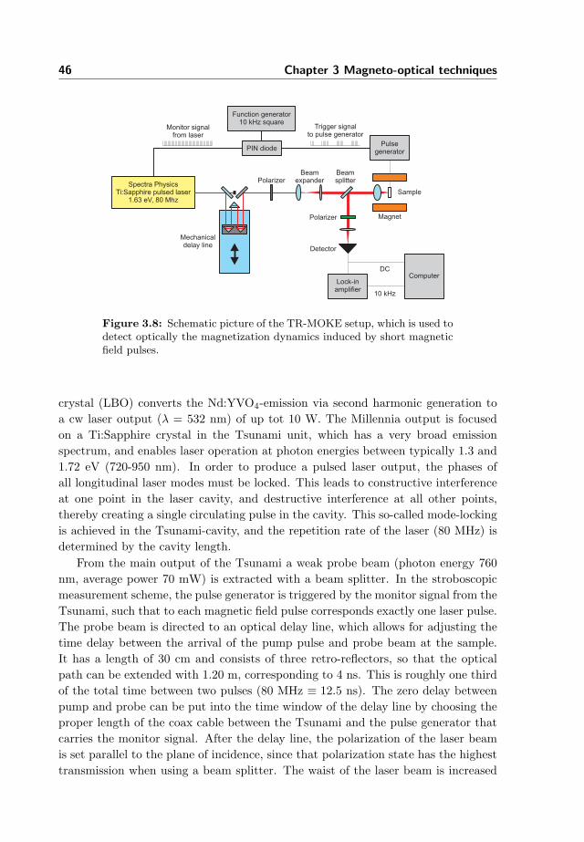
46 Chapter 3 Magneto-optical techniques
Spectra PhysicsTi:Sapphire pulsed laser
1.63 eV, 80 Mhz
PIN diode
Monitor signalfrom laser
Function generator10 kHz square
Trigger signalto pulse generator
Pulsegenerator
Mechanicaldelay line
PolarizerBeam
expanderBeamsplitter
Polarizer
Detector
Magnet
Sample
Lock-inamplifier
Computer
10 kHz
DC
Figure 3.8: Schematic picture of the TR-MOKE setup, which is used todetect optically the magnetization dynamics induced by short magneticfield pulses.
crystal (LBO) converts the Nd:YVO4-emission via second harmonic generation toa cw laser output (λ = 532 nm) of up tot 10 W. The Millennia output is focusedon a Ti:Sapphire crystal in the Tsunami unit, which has a very broad emissionspectrum, and enables laser operation at photon energies between typically 1.3 and1.72 eV (720-950 nm). In order to produce a pulsed laser output, the phases ofall longitudinal laser modes must be locked. This leads to constructive interferenceat one point in the laser cavity, and destructive interference at all other points,thereby creating a single circulating pulse in the cavity. This so-called mode-lockingis achieved in the Tsunami-cavity, and the repetition rate of the laser (80 MHz) isdetermined by the cavity length.
From the main output of the Tsunami a weak probe beam (photon energy 760nm, average power 70 mW) is extracted with a beam splitter. In the stroboscopicmeasurement scheme, the pulse generator is triggered by the monitor signal from theTsunami, such that to each magnetic field pulse corresponds exactly one laser pulse.The probe beam is directed to an optical delay line, which allows for adjusting thetime delay between the arrival of the pump pulse and probe beam at the sample.It has a length of 30 cm and consists of three retro-reflectors, so that the opticalpath can be extended with 1.20 m, corresponding to 4 ns. This is roughly one thirdof the total time between two pulses (80 MHz ≡ 12.5 ns). The zero delay betweenpump and probe can be put into the time window of the delay line by choosing theproper length of the coax cable between the Tsunami and the pulse generator thatcarries the monitor signal. After the delay line, the polarization of the laser beamis set parallel to the plane of incidence, since that polarization state has the highesttransmission when using a beam splitter. The waist of the laser beam is increased

3.2 TR-MOKE 47
0 1 2 3
-1.0
-0.5
0.0
0.5
1.0
Mz /
Ms (
10-2
Ms )
Delay time (ns)
Figure 3.9: Example of a TR-MOKE measurement obtained on a 13×9µm magnetic (Ni80Fe20) element. The precessional motion is triggered bya magnetic field pulse induced by a current line. The external magneticfield was set to 2.5 mT.
with the use of a beam expander in order to cover the full aperture of a 0.65 NA(numerical aperture) microscope objective, which focuses the probe beam on thesample. With this objective, the theoretical diffraction limited spot size is 1.5 µm.The sample holder is mounted on a x− y− z motorized translation stage for accuratepositioning and focusing. A magnetic bias field up to 8 kA/m can be applied parallelto the current line with a homemade electromagnet. The reflected probe beam fromthe sample travels backwards into the objective, and is directed to the detector bythe beam splitter. It passes a second polarizer with its axis 45◦ relative to that ofthe first polarizer, and is finally focused on the Si-photodiode. Due to the normalincidence of the probe beam, the setup is only sensitive to the polar Kerr-effect, andthus to out-of-plane magnetization. We note that in this configuration preferablythe Kerr-rotation is measured, since its sensitivity to out-of-plane magnetization ishigher than for Kerr-ellipticity.
However, the Kerr-effect is still very small, and in order to detect it, a modulationscheme is used. The 80 MHz monitor signal from the Ti-sapphire laser system, thatfunctions as the trigger signal for the pulse generator, is sent through a PIN-diode,to which a 10 kHz square wave gate signal is supplied. The monitor signal is thusmodulated with 10 kHz, and as a result, the magnetic pulses that induce the fastmagnetization dynamics are modulated into 10 kHz pulse trains, see Fig. 3.8. Thedetector signal will then contain a 10 kHz component, which is extracted with theuse of a Stanford Research Systems Digital Signal Processing (DSP) lock-in amplifier(model SR830). Signal-to-noise ratios up to 200:1 can be achieved this way. It isimportant to stress that the lock-in signal is linearly proportional to the change inKerr-rotation of the reflected probe beam due to the output current of the pulse
48 Chapter 3 Magneto-optical techniques
generator. The intensity signal was measured simultaneously with the lock-in signal,by extracting the DC-signal with a low-pass filter.
A typical example of a TR-MOKE measurement, taken on a micron sized mag-netic (Ni80Fe20) element using magnetic field pulses, is shown in Fig. 3.9. At t = 0ns a precessional motion is launched, which shows similar characteristics as themodeled response presented in Fig. 2.2a. The response after ≈ 0.6 ns, when themagnetic field pulse has ended, can be well described by a damped sine wave with afrequency of 2.4 GHz and a decay time of 2.1 ns. This decay time corresponds to adamping parameter of α ≈ 0.008 (see Eq. 2.2), which is characteristic for Ni80Fe20
[21]. In Chapter 4 we will explore this precessional motion in more detail, and studyits spatial and magnetic field dependence.
3.3 TiMMS
Time-resolved Magnetization Modulation Spectroscopy (TiMMS) [22] is a very ver-satile technique to study spin dynamics in semiconductors, and is the main exper-imental tool in Chapters 5, 6, and 7. It is a stroboscopic measurement techniqueaccording to an all-optical pump-probe scheme. In short, a strong circularly po-larized laser pulse excites an electron and hole spin population in a semiconductorvia the optical selection rules of the zinc-blende crystal structure. A second, muchweaker probe laser pulse measures the evolution of the spin population via themagneto-optical Kerr-effect. The time-difference between arrival of the pump andprobe pulse on the semiconductor is controlled by a mechanical translation stage,thereby enabling time-resolved measurements of the excited spin population. Bytuning the laser photon energy, full spectroscopic data of the semiconductor underinvestigation can be obtained. In this Section, we will present the details of theexperimental TiMMS-setup, present the signal analysis, and show some illustrativeexamples of TiMMS-measurements on a spin injection device.
3.3.1 TiMMS-setup
The TiMMS measurements shown in this Thesis are obtained with the experimentalsetup as schematically shown in Fig. 3.10. The same Spectra-Physics laser systemas used in the TR-MOKE setup is employed as a pulsed laser source. It is extendedwith Lock-to-Clock electronics, which enables synchronization of this laser systemwith another pulsed laser. This allows two-color experiments with independentlytunable laser photon energies for pump and probe beam, even for small differencesin laser photon energies (e.g. by locking two Tsunami laser systems).
The output beam of the Tsunami is divided into a strong pump and a muchweaker probe pulse with a beamsplitter. The pump beam passes two cube polarizersand a photo-elastic modulator (PEM) before being directed towards a magneto-optical cryostat by a second beam splitter. By tuning the relative angle between
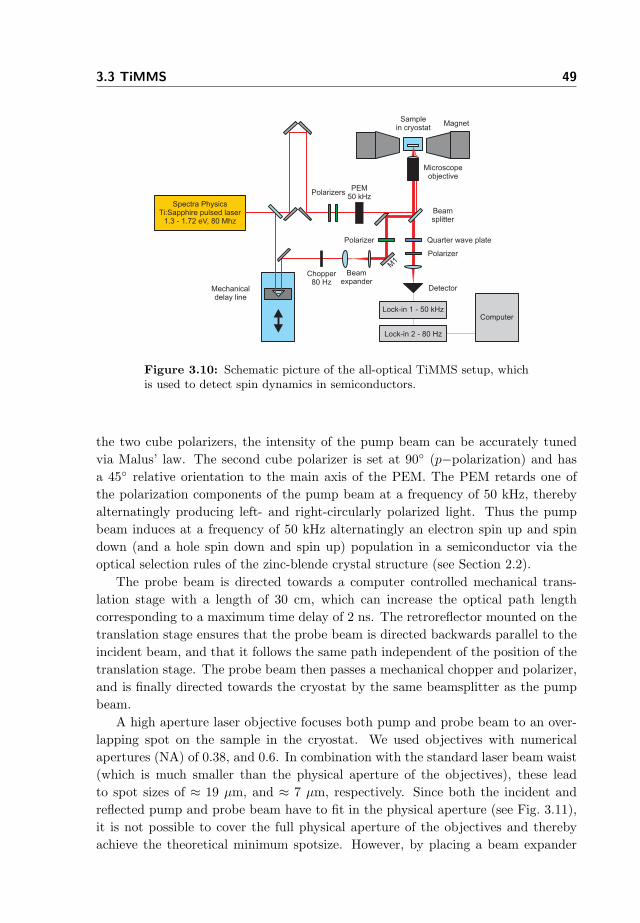
3.3 TiMMS 49
Spectra PhysicsTi:Sapphire pulsed laser
1.3 - 1.72 eV, 80 Mhz
Mechanicaldelay line
Polarizers
Beamsplitter
Beamexpander
Polarizer
Detector
MagnetSample
in cryostat
Polarizer
Chopper80 Hz
PEM50 kHz
Microscopeobjective
Computer
Lock-in 2 - 80 Hz
Lock-in 1 - 50 kHz
M1
Quarter wave plate
Figure 3.10: Schematic picture of the all-optical TiMMS setup, whichis used to detect spin dynamics in semiconductors.
the two cube polarizers, the intensity of the pump beam can be accurately tunedvia Malus’ law. The second cube polarizer is set at 90◦ (p−polarization) and hasa 45◦ relative orientation to the main axis of the PEM. The PEM retards one ofthe polarization components of the pump beam at a frequency of 50 kHz, therebyalternatingly producing left- and right-circularly polarized light. Thus the pumpbeam induces at a frequency of 50 kHz alternatingly an electron spin up and spindown (and a hole spin down and spin up) population in a semiconductor via theoptical selection rules of the zinc-blende crystal structure (see Section 2.2).
The probe beam is directed towards a computer controlled mechanical trans-lation stage with a length of 30 cm, which can increase the optical path lengthcorresponding to a maximum time delay of 2 ns. The retroreflector mounted on thetranslation stage ensures that the probe beam is directed backwards parallel to theincident beam, and that it follows the same path independent of the position of thetranslation stage. The probe beam then passes a mechanical chopper and polarizer,and is finally directed towards the cryostat by the same beamsplitter as the pumpbeam.
A high aperture laser objective focuses both pump and probe beam to an over-lapping spot on the sample in the cryostat. We used objectives with numericalapertures (NA) of 0.38, and 0.6. In combination with the standard laser beam waist(which is much smaller than the physical aperture of the objectives), these leadto spot sizes of ≈ 19 µm, and ≈ 7 µm, respectively. Since both the incident andreflected pump and probe beam have to fit in the physical aperture (see Fig. 3.11),it is not possible to cover the full physical aperture of the objectives and therebyachieve the theoretical minimum spotsize. However, by placing a beam expander

50 Chapter 3 Magneto-optical techniques
0 10 20 30 40 50 600
10
20
30
40
50
Position (mm)
Po
sitio
n(m
m)
0 10 20 30 40 50 600
10
20
30
40
50
Position (mm)
Po
sitio
n(m
m)
0 10 20 30 40 50 600
10
20
30
40
50
Position (mm)
Po
sitio
n(m
m)
(a) (c)(b)NA 0.38 NA 0.60 NA 0.60
pump
probe
Figure 3.11: Raster scans of the same part of a marker sample withsemiconductor nanowires, taken with different objectives, laser beamwaists, and position of incidence, as indicated by the schematic illustra-tions of objective and probe beam. The effect on the spatial resolutionis immediate.
in the path of the probe beam, thereby increasing the laser beam waist by a factorof 2, the spot size of the probe beam on the sample could be reduced by the samefactor to ≈ 9.5 µm, and ≈ 3.5 µm, respectively. We note that only when the probebeam is incident on the optical axis of the objective (thus through the center ofthe objective), a minimum spot size in the two lateral directions can be obtained.Figure 3.11 shows the effect of both the laser beam waist, and the position of inci-dence relative to the optical axis, on the final resolution of a raster scan on a markersample containing semiconductor nanowires.
The reflected probe beam passes the beamsplitter, followed by a quarter-waveplate, a polarizer (the so-called analyzer), and is finally incident on the detector.The signal from the detector (a silicon photo-diode with amplification electronics)is sent to a first lock-in amplifier (Stanford Research Systems model SR830) lockedto the reference frequency of the PEM (50 kHz). The output of the first lock-inamplifier serves as the input of a second lock-in amplifier, locked to the referencefrequency of the chopper (typically 80 Hz). This double modulation scheme allowsthe detection of the generally small magneto-optical Kerr-effect, and ensures thatonly pump induced changes of the dielectric tensor of the sample are detected. Onehas to take care that the inverse time-constant of the first lock-in amplifier is muchsmaller than the reference frequency of the second lock-in amplifier, see Table 3.1.
The resulting signal output of the second lock-in amplifier depends on the set-tings of the quarter-wave plate and analyzer. In the following Section the signalanalysis of the TiMMS technique using the Jones-formalism will be outlined.
Returning to the setup shown in Fig. 3.10, we note that the objective is mountedto a x−y−z−motorized translation stage system, facilitating accurate positioning of
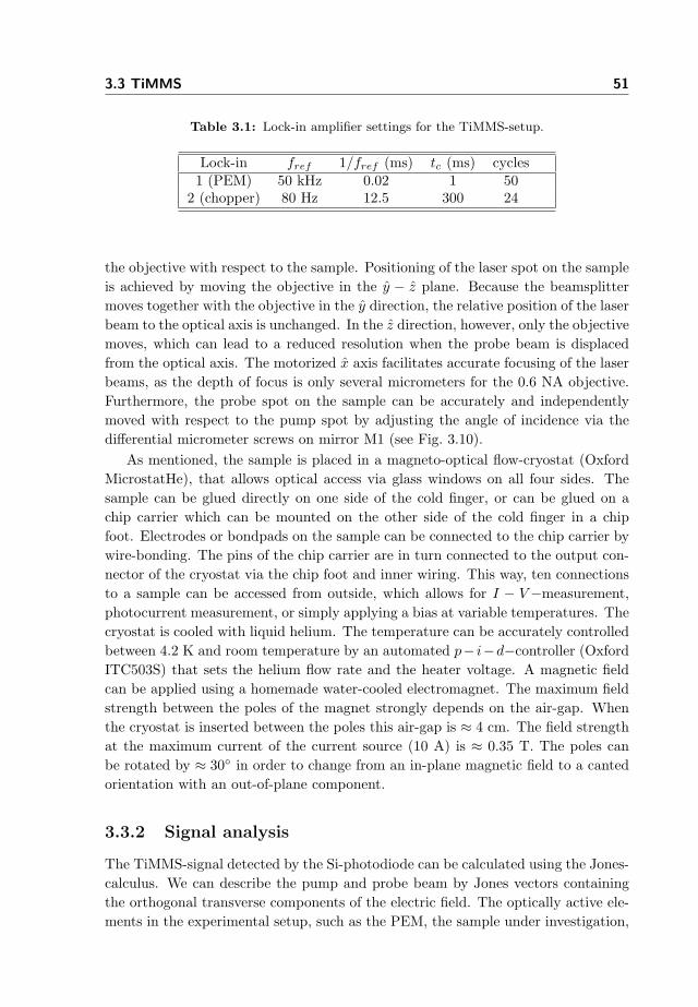
3.3 TiMMS 51
Table 3.1: Lock-in amplifier settings for the TiMMS-setup.
Lock-in fref 1/fref (ms) tc (ms) cycles1 (PEM) 50 kHz 0.02 1 50
2 (chopper) 80 Hz 12.5 300 24
the objective with respect to the sample. Positioning of the laser spot on the sampleis achieved by moving the objective in the y − z plane. Because the beamsplittermoves together with the objective in the y direction, the relative position of the laserbeam to the optical axis is unchanged. In the z direction, however, only the objectivemoves, which can lead to a reduced resolution when the probe beam is displacedfrom the optical axis. The motorized x axis facilitates accurate focusing of the laserbeams, as the depth of focus is only several micrometers for the 0.6 NA objective.Furthermore, the probe spot on the sample can be accurately and independentlymoved with respect to the pump spot by adjusting the angle of incidence via thedifferential micrometer screws on mirror M1 (see Fig. 3.10).
As mentioned, the sample is placed in a magneto-optical flow-cryostat (OxfordMicrostatHe), that allows optical access via glass windows on all four sides. Thesample can be glued directly on one side of the cold finger, or can be glued on achip carrier which can be mounted on the other side of the cold finger in a chipfoot. Electrodes or bondpads on the sample can be connected to the chip carrier bywire-bonding. The pins of the chip carrier are in turn connected to the output con-nector of the cryostat via the chip foot and inner wiring. This way, ten connectionsto a sample can be accessed from outside, which allows for I − V−measurement,photocurrent measurement, or simply applying a bias at variable temperatures. Thecryostat is cooled with liquid helium. The temperature can be accurately controlledbetween 4.2 K and room temperature by an automated p− i−d−controller (OxfordITC503S) that sets the helium flow rate and the heater voltage. A magnetic fieldcan be applied using a homemade water-cooled electromagnet. The maximum fieldstrength between the poles of the magnet strongly depends on the air-gap. Whenthe cryostat is inserted between the poles this air-gap is ≈ 4 cm. The field strengthat the maximum current of the current source (10 A) is ≈ 0.35 T. The poles canbe rotated by ≈ 30◦ in order to change from an in-plane magnetic field to a cantedorientation with an out-of-plane component.
3.3.2 Signal analysis
The TiMMS-signal detected by the Si-photodiode can be calculated using the Jones-calculus. We can describe the pump and probe beam by Jones vectors containingthe orthogonal transverse components of the electric field. The optically active ele-ments in the experimental setup, such as the PEM, the sample under investigation,
52 Chapter 3 Magneto-optical techniques
polarizers, and quarter wave-plates, are described by Jones-matrices. Let us startwith the pump beam. The polarization of the pump beam at the sample is given byits initial polarization vector, ~E0
pu, multiplied with the Jones-matrix of the PEM,MPEM . Following the setup of Fig. 3.10, the polarization vector at the sampleposition, ~Esam
pu , is given as
~Esampu = Mrot(−45) ·MPEM ·Mrot(45) · ~E0
pu (3.17)
with Mrot(α) the Jones-matrix for a rotation over α degrees. Writing down the fullmatrices, we have
~Esampu =
1√2
(1 1−1 1
)·(
1 00 exp[ıA(t)]
)· 1√
2
(1 −11 1
)· E0
pu
(01
)(3.18)
with E0pu the amplitude of the pump beam, A(t) = A0 cos(2πft), A0 the PEM
retardation, and f the operating frequency of the PEM. Equation 3.18 results aftersome algebra in
~Esampu = E0
pu
[A+(t)
1√2
(1ı
)+ A−(t)
1√2
(1−ı
)](3.19)
with A±(t) = (1± ı)(±ı + exp[ıA(t)])/2√
2. From 3.19 it follows that the polariza-tion of the pump beam at the sample alternates between left- and right-circularlypolarized light at a frequency f . Via the optical selection rules a net spin populationis induced, proportional to |A+|2 − |A−|2 = sin[A(t)], which leads to non-vanishingoff-diagonal elements of the dielectric tensor of the sample. This in turn leads to acomplex Kerr-rotation of the probe beam, whose polarization state at the detector,~Edet
pr (following again Fig. 3.10) can be written as
~Edetpr = MPOL ·MQWP (45) ·Msam · ~E0
pr (3.20)
with ~E0pr the s−polarization of the incident probe beam, Msam, MQWP (45), and
MPOL the Jones-matrices of the sample, quarter-wave plate and polarizer, respec-tively. Writing again the full matrices, we obtain
~Edetpr =
(1 00 0
)· (1 + ı)
2
(1 ıı 1
)·(
rss rspθ(t)rpsθ(t) rpp
)· E0
pr
(10
)(3.21)
with E0pr the amplitude of the probe beam, and θ(t) = sin[A(t)]. After some algebra,
Eq. 3.21 can be simplified to
~Edetpr =
Epr
2(1 + ı)
(rss − ırpsθ(t)
0
). (3.22)
From Eq. 3.23 it follows that the complex Kerr-rotation of the probe beam oscillateswith the frequency of the PEM, as expected. The voltage-output of the detector is

3.3 TiMMS 53
GaAs substrate
AlOx tunnel barrier
n GaAs doping layers
n-GaAs 5 10 cm (200 nm)
Si -doping 2 10 cm
++
16 -3
11 -2d
Al Ga As undoped (200 nm)0.3 0.7
Figure 3.12: Schematic layout of the semiconductor heterostructure,which is the basis for an all-electrical spin injection and detection device,proposed by and fabricated at IMEC Leuven [23].
then given by
Vdet ∝ ( ~E0pr)
∗ ~E0pr =
(E0
prrss
2
)2
×(
2 +r2ps
r2ss
+ 4<(rss)=(rps)−=(rss)<(rps)
r2ss
sin[A(t)]− r2ps
r2ss
cos[A(t)]
). (3.23)
Expanding the terms sin[A(t)] = sin[A0 cos(2πft)] and cos[A(t)] = cos[A0 cos(2πft)]in Bessel-function of the first kind, we find for the ratio of the 1f and dc componentsof the detector signal
V1f
Vdc= 4J1(A0)εK . (3.24)
V1f is thus proportional to the Kerr-ellipticity. If the angle of the final polarizer isset to 45◦, it can be shown that V1f is proportional to the Kerr-rotation.
3.3.3 An example: TiMMS on a spin injection device
As an example of the capabilities of the TiMMS-setup, we show results of spinrelaxation and spin diffusion measurements on samples originally designed for all-electrical spin injection and detection in GaAs. The samples were grown at IMECLeuven [23], and the common layout is schematically shown in Fig. 3.12. All samplesconsist of a AlOx tunnel barrier, a 200-nm GaAs spin transport channel, with highdoping layers near the top surface, and an Al0.3Ga0.7As blocking layer at the bottom.The Al0.3Ga0.7As blocking layer facilitates a confined current flow in the lateraldirections, by prohibiting current flow in the vertical direction. The Si δ-doping inthe Al0.3Ga0.7As layer is inserted to render the device insensitive to surface depletionand variations in the etching process. The heterostructure is grown on a semi-insulating GaAs substrate. Ferromagnetic contacts and the tunnel injector are not
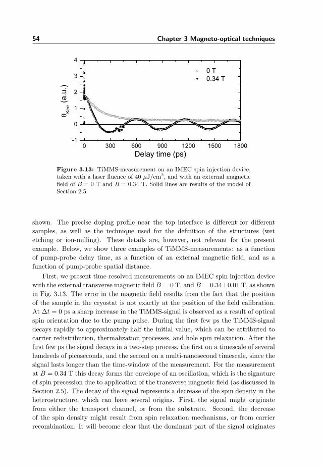
54 Chapter 3 Magneto-optical techniques
0 300 600 900 1200 1500 1800-1
0
1
2
3
4
0 T 0.34 T
Ker
r (a.u
.)
Delay time (ps)
Figure 3.13: TiMMS-measurement on an IMEC spin injection device,taken with a laser fluence of 40 µJ/cm2, and with an external magneticfield of B = 0 T and B = 0.34 T. Solid lines are results of the model ofSection 2.5.
shown. The precise doping profile near the top interface is different for differentsamples, as well as the technique used for the definition of the structures (wetetching or ion-milling). These details are, however, not relevant for the presentexample. Below, we show three examples of TiMMS-measurements: as a functionof pump-probe delay time, as a function of an external magnetic field, and as afunction of pump-probe spatial distance.
First, we present time-resolved measurements on an IMEC spin injection devicewith the external transverse magnetic field B = 0 T, and B = 0.34±0.01 T, as shownin Fig. 3.13. The error in the magnetic field results from the fact that the positionof the sample in the cryostat is not exactly at the position of the field calibration.At ∆t = 0 ps a sharp increase in the TiMMS-signal is observed as a result of opticalspin orientation due to the pump pulse. During the first few ps the TiMMS-signaldecays rapidly to approximately half the initial value, which can be attributed tocarrier redistribution, thermalization processes, and hole spin relaxation. After thefirst few ps the signal decays in a two-step process, the first on a timescale of severalhundreds of picoseconds, and the second on a multi-nanosecond timescale, since thesignal lasts longer than the time-window of the measurement. For the measurementat B = 0.34 T this decay forms the envelope of an oscillation, which is the signatureof spin precession due to application of the transverse magnetic field (as discussed inSection 2.5). The decay of the signal represents a decrease of the spin density in theheterostructure, which can have several origins. First, the signal might originatefrom either the transport channel, or from the substrate. Second, the decreaseof the spin density might result from spin relaxation mechanisms, or from carrierrecombination. It will become clear that the dominant part of the signal originates

3.3 TiMMS 55
from the transport channel, and that the first (0-400 ps) decay-process is due tocarrier recombination, and the second (> ns) is due to spin relaxation.
A closer look on the measurement at B = 0.34 T reveals that the period of theoscillation starting from the first maximum at ∆t = 603 ps is constant and equalto 554 ps. Clearly, this shows that the period of the first full oscillation is longerby 48 ps (or ≈ 9%). As the phase of the precession at ∆t = 0 is zero (i.e. all spinsare aligned normal to the sample surface, and hence the TiMMS-signal is maximal),this means that during the first few hundred ps these spins precess with a lowerfrequency. A slower precession might be caused by a lower g factor. Also, it isknown that the electron g factor decreases with higher electron energy, as statedin Section 2.5. With the laser fluence of the experiment, we expect an opticallyinduced carrier density well above 1017 cm−3. With this density, electrons at theelectron quasi Fermi-level will have a lower g factor than those near the band edge.Recombination lowers the electron quasi Fermi-level, which increases the g factor.We thus conjecture that the phase shift is caused by a carrier density effect, via atime-dependent electron g factor.
This conjecture implies that recombination takes place during the first few hun-dred ps. We have already examined the effect of a relative high laser induced carrierdensity and recombination on the spin relaxation, with the model of Section 2.4.It was found that initially, recombination is the dominant source of decay of thespin density, and that after recombination the spin relaxation time is determinedby the donor concentration, see Fig. 2.7c. Qualitatively, the model shows the mainfeatures of the experimental result with B = 0 T, in agreement with our conjec-ture. It is, however, not possible to simulate the exact measured time-trace withthe model. One reason might be that the recombination parameter is not constant,as the precise band alignment in the transport channel depends on the free carrierdensity. At low carrier densities, a small internal electric field exists due to Fermilevel pinning at the tunnel barrier. This internal electric field can separate freeelectrons and holes, leading to a lower recombination rate, and a different decay ofthe spin polarization. A second reason might be that the measurement data con-tains a weak signal originating from the substrate. Because the substrate consistsof semi-insulating GaAs, this possible signal is only expected to be present duringthe first few hundred ps [24].
Using the model of Section 2.5 to simulate the spin precession data, we canachieve a very nice agreement with the experimental data when using an opticallyinduced carrier density of 1.5·1017 cm−3, a recombination time of 180 ps, a magneticfield of B = 0.333 T, and a final spin polarization of 1.0 · 1016 cm−3. This resultsupports our conjecture that the main experimental features of Fig. 3.13 are theresult of recombination and a carrier density dependent electron g factor.
We already mentioned that the second decay process is due to spin relaxationin the transport channel. From Fig. 3.13 it is, however, difficult to extract the spinrelaxation time. From the donor concentration, a spin relaxation time of 30 − 40
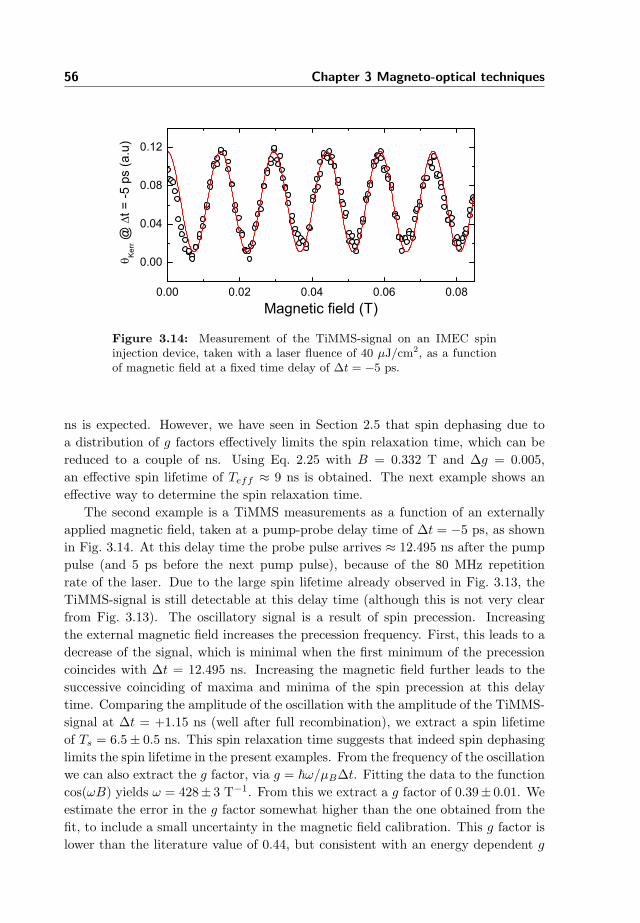
56 Chapter 3 Magneto-optical techniques
0.00 0.02 0.04 0.06 0.08
0.00
0.04
0.08
0.12
Ker
r @
t = -5
ps
(a.u
)
Magnetic field (T)
Figure 3.14: Measurement of the TiMMS-signal on an IMEC spininjection device, taken with a laser fluence of 40 µJ/cm2, as a functionof magnetic field at a fixed time delay of ∆t = −5 ps.
ns is expected. However, we have seen in Section 2.5 that spin dephasing due toa distribution of g factors effectively limits the spin relaxation time, which can bereduced to a couple of ns. Using Eq. 2.25 with B = 0.332 T and ∆g = 0.005,an effective spin lifetime of Teff ≈ 9 ns is obtained. The next example shows aneffective way to determine the spin relaxation time.
The second example is a TiMMS measurements as a function of an externallyapplied magnetic field, taken at a pump-probe delay time of ∆t = −5 ps, as shownin Fig. 3.14. At this delay time the probe pulse arrives ≈ 12.495 ns after the pumppulse (and 5 ps before the next pump pulse), because of the 80 MHz repetitionrate of the laser. Due to the large spin lifetime already observed in Fig. 3.13, theTiMMS-signal is still detectable at this delay time (although this is not very clearfrom Fig. 3.13). The oscillatory signal is a result of spin precession. Increasingthe external magnetic field increases the precession frequency. First, this leads to adecrease of the signal, which is minimal when the first minimum of the precessioncoincides with ∆t = 12.495 ns. Increasing the magnetic field further leads to thesuccessive coinciding of maxima and minima of the spin precession at this delaytime. Comparing the amplitude of the oscillation with the amplitude of the TiMMS-signal at ∆t = +1.15 ns (well after full recombination), we extract a spin lifetimeof Ts = 6.5± 0.5 ns. This spin relaxation time suggests that indeed spin dephasinglimits the spin lifetime in the present examples. From the frequency of the oscillationwe can also extract the g factor, via g = ~ω/µB∆t. Fitting the data to the functioncos(ωB) yields ω = 428± 3 T−1. From this we extract a g factor of 0.39± 0.01. Weestimate the error in the g factor somewhat higher than the one obtained from thefit, to include a small uncertainty in the magnetic field calibration. This g factor islower than the literature value of 0.44, but consistent with an energy dependent g
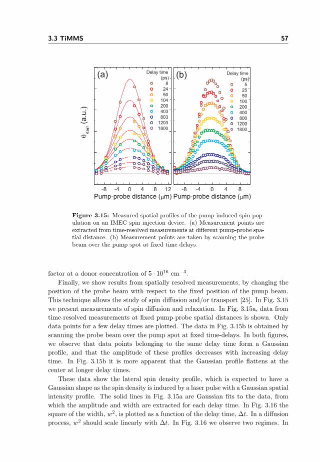
3.3 TiMMS 57
-8 -4 0 4 8 12
Delay time
(ps)
8
24
50
104
200
403
803
1203
1800
qK
err
(a.u
.)
Pump-probe distance (mm)-8 -4 0 4 8
Delay time
(ps)
5
25
50
100
200
400
800
1200
1800
Pump-probe distance (mm)
(a) (b)
Figure 3.15: Measured spatial profiles of the pump-induced spin pop-ulation on an IMEC spin injection device. (a) Measurement points areextracted from time-resolved measurements at different pump-probe spa-tial distance. (b) Measurement points are taken by scanning the probebeam over the pump spot at fixed time delays.
factor at a donor concentration of 5 · 1016 cm−3.Finally, we show results from spatially resolved measurements, by changing the
position of the probe beam with respect to the fixed position of the pump beam.This technique allows the study of spin diffusion and/or transport [25]. In Fig. 3.15we present measurements of spin diffusion and relaxation. In Fig. 3.15a, data fromtime-resolved measurements at fixed pump-probe spatial distances is shown. Onlydata points for a few delay times are plotted. The data in Fig. 3.15b is obtained byscanning the probe beam over the pump spot at fixed time-delays. In both figures,we observe that data points belonging to the same delay time form a Gaussianprofile, and that the amplitude of these profiles decreases with increasing delaytime. In Fig. 3.15b it is more apparent that the Gaussian profile flattens at thecenter at longer delay times.
These data show the lateral spin density profile, which is expected to have aGaussian shape as the spin density is induced by a laser pulse with a Gaussian spatialintensity profile. The solid lines in Fig. 3.15a are Gaussian fits to the data, fromwhich the amplitude and width are extracted for each delay time. In Fig. 3.16 thesquare of the width, w2, is plotted as a function of the delay time, ∆t. In a diffusionprocess, w2 should scale linearly with ∆t. In Fig. 3.16 we observe two regimes. In
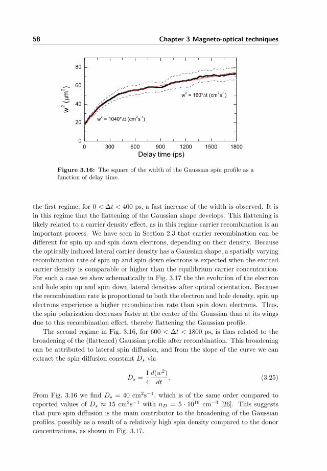
58 Chapter 3 Magneto-optical techniques
0 300 600 900 1200 1500 18000
20
40
60
80
w2 = 160* t (cm2s-1)
w2 (
m2 )
Delay time (ps)
w2 = 1040* t (cm2s-1)
Figure 3.16: The square of the width of the Gaussian spin profile as afunction of delay time.
the first regime, for 0 < ∆t < 400 ps, a fast increase of the width is observed. It isin this regime that the flattening of the Gaussian shape develops. This flattening islikely related to a carrier density effect, as in this regime carrier recombination is animportant process. We have seen in Section 2.3 that carrier recombination can bedifferent for spin up and spin down electrons, depending on their density. Becausethe optically induced lateral carrier density has a Gaussian shape, a spatially varyingrecombination rate of spin up and spin down electrons is expected when the excitedcarrier density is comparable or higher than the equilibrium carrier concentration.For such a case we show schematically in Fig. 3.17 the the evolution of the electronand hole spin up and spin down lateral densities after optical orientation. Becausethe recombination rate is proportional to both the electron and hole density, spin upelectrons experience a higher recombination rate than spin down electrons. Thus,the spin polarization decreases faster at the center of the Gaussian than at its wingsdue to this recombination effect, thereby flattening the Gaussian profile.
The second regime in Fig. 3.16, for 600 < ∆t < 1800 ps, is thus related to thebroadening of the (flattened) Gaussian profile after recombination. This broadeningcan be attributed to lateral spin diffusion, and from the slope of the curve we canextract the spin diffusion constant Ds via
Ds =14
d(w2)dt
. (3.25)
From Fig. 3.16 we find Ds = 40 cm2s−1, which is of the same order compared toreported values of Ds ≈ 15 cm2s−1 with nD = 5 · 1016 cm−3 [26]. This suggeststhat pure spin diffusion is the main contributor to the broadening of the Gaussianprofiles, possibly as a result of a relatively high spin density compared to the donorconcentrations, as shown in Fig. 3.17.
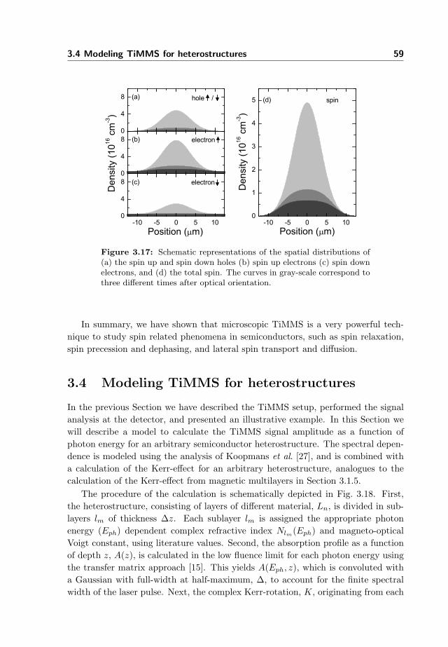
3.4 Modeling TiMMS for heterostructures 59
-10 -5 0 5 100
1
2
3
4
5
Position ( m)
Den
sity
(1016
cm
-3)
Position ( m)-10 -5 0 5 10
0
4
8
Den
sity
(1016
cm
-3)
0
4
8
0
4
8 spin
electron
electron
hole / (d)
(c)
(b)
(a)
Figure 3.17: Schematic representations of the spatial distributions of(a) the spin up and spin down holes (b) spin up electrons (c) spin downelectrons, and (d) the total spin. The curves in gray-scale correspond tothree different times after optical orientation.
In summary, we have shown that microscopic TiMMS is a very powerful tech-nique to study spin related phenomena in semiconductors, such as spin relaxation,spin precession and dephasing, and lateral spin transport and diffusion.
3.4 Modeling TiMMS for heterostructures
In the previous Section we have described the TiMMS setup, performed the signalanalysis at the detector, and presented an illustrative example. In this Section wewill describe a model to calculate the TiMMS signal amplitude as a function ofphoton energy for an arbitrary semiconductor heterostructure. The spectral depen-dence is modeled using the analysis of Koopmans et al. [27], and is combined witha calculation of the Kerr-effect for an arbitrary heterostructure, analogues to thecalculation of the Kerr-effect from magnetic multilayers in Section 3.1.5.
The procedure of the calculation is schematically depicted in Fig. 3.18. First,the heterostructure, consisting of layers of different material, Ln, is divided in sub-layers lm of thickness ∆z. Each sublayer lm is assigned the appropriate photonenergy (Eph) dependent complex refractive index Nlm(Eph) and magneto-opticalVoigt constant, using literature values. Second, the absorption profile as a functionof depth z, A(z), is calculated in the low fluence limit for each photon energy usingthe transfer matrix approach [15]. This yields A(Eph, z), which is convoluted witha Gaussian with full-width at half-maximum, ∆, to account for the finite spectralwidth of the laser pulse. Next, the complex Kerr-rotation, K, originating from each

60 Chapter 3 Magneto-optical techniques
Structurelayers Ln
Sublayerslm
N(E,z)
Q(E,z)
KerrK(E,z)
AbsorptionA(E,z)
TiMMST(E,z)
TiMMST (E)Ln
Figure 3.18: Modeling scheme for the TiMMS-signal originating fromheterostructures.
lm is calculated for each photon energy using the matrix approach of Zak et al.(see Section 3.1.4). This is done by calculating the complex Kerr-rotation of thefull heterostructure, while artificially setting only for a single sublayer lm a nonzerocomplex magneto-optical Voigt parameter, in a similar way as in Section 3.1.5 forthe CoPt-multilayer. Finally, the calculation yields K(Eph, z). Using this A(Eph, z)and K(Eph, z) the TiMMS spectral response of each sublayer lm, T (Eph, z), canbe calculated following Koopmans et al. [27], which we shall briefly discuss in thefollowing.
The pump and probe pulses from the Ti:Sapphire laser in the experiment havea Gaussian spectral shape, and can be written as
In(En) = An exp
(−
[(E − En)
∆
]2)
, (3.26)
with An the amplitude, and En the center photon energy, with n = pu, pr for thepump and probe pulse, respectively. Absorption of a circularly polarized pump pulseleads, via the optical selection rules, to an excited spin polarized electron (hole) den-sity in the conduction (valence) band, denoted as ne,σ(E), and nh,σ(E), respectively,with σ = ± for spin up and spin down. Since the hole spin relaxation rate is muchfaster than the electron spin relaxation rate for bulk III-V semiconductors, we willonly consider the electron spin density. Also, we will consider a fully thermalizedelectron system, which is appropriate for delay times larger than the electron ther-malization time of typically one ps. The spectral profile of the electron spin densityis determined by the total amount of excited carriers, Ne, the density of states, andthe temperature, T . In the model, we use the absorption profile A(Epu, z) of thepump pulse to determine Ne in every sublayer lm for each Epu. Using a 3D densityof states (see Eq. 2.14, and a Fermi-Dirac-distribution of the electrons, the electrondensity can be written as
ne(E) = 8π√
2(me
h2
)3/2√
E − Eg
exp E−EF (Ne)kBT + 1
, (3.27)
with me the electron effective mass in the conduction band, Eg the bandgap of thematerial, EF (Ne) the electron quasi-Fermi level after laser excitation corresponding
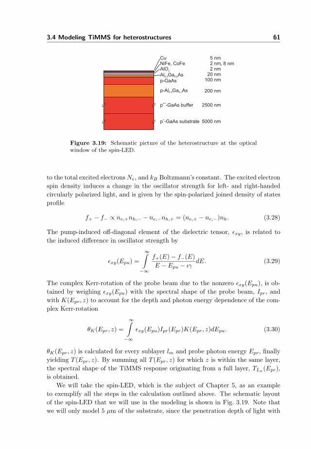
3.4 Modeling TiMMS for heterostructures 61
p -GaAs buffer++
p-Al Ga As0.3 0.7
CuNiFe, CoFeAlO
Al Ga As
p-GaAs
x
0.2 0.8
p -GaAs substrate+
5 nm2 nm2 nm
20 nm100 nm
, 8 nm
200 nm
2500 nm
5000 nm
Figure 3.19: Schematic picture of the heterostructure at the opticalwindow of the spin-LED.
to the total excited electrons Ne, and kB Boltzmann’s constant. The excited electronspin density induces a change in the oscillator strength for left- and right-handedcircularly polarized light, and is given by the spin-polarized joined density of statesprofile
f+ − f− ∝ ne,+nh,− − ne,−nh,+ = (ne,+ − ne,−)nh. (3.28)
The pump-induced off-diagonal element of the dielectric tensor, εxy, is related tothe induced difference in oscillator strength by
εxy(Epu) =
∞∫
−∞
f+(E)− f−(E)E − Epu − ıγ
dE. (3.29)
The complex Kerr-rotation of the probe beam due to the nonzero εxy(Epu), is ob-tained by weighing εxy(Epu) with the spectral shape of the probe beam, Ipr, andwith K(Epr, z) to account for the depth and photon energy dependence of the com-plex Kerr-rotation
θK(Epr, z) =
∞∫
−∞εxy(Epu)Ipr(Epr)K(Epr, z)dEpu. (3.30)
θK(Epr, z) is calculated for every sublayer lm and probe photon energy Epr, finallyyielding T (Epr, z). By summing all T (Epr, z) for which z is within the same layer,the spectral shape of the TiMMS response originating from a full layer, TLn(Epr),is obtained.
We will take the spin-LED, which is the subject of Chapter 5, as an exampleto exemplify all the steps in the calculation outlined above. The schematic layoutof the spin-LED that we will use in the modeling is shown in Fig. 3.19. Note thatwe will only model 5 µm of the substrate, since the penetration depth of light with
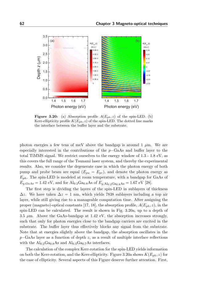
62 Chapter 3 Magneto-optical techniques
1.4 1.5 1.6 1.7
Photon energy (eV)
0.30
0.22
0.15
0.07
0
-0.07
-0.15
-0.23
-0.30
1.4 1.5 1.6 1.70.0
0.5
1.0
1.5
2.0
2.5
3.0
3.5
(b)(a)K(E
ph,z)
(a.u.)
Photon energy (eV)
De
pth
z(m
m)
0
6.3E-4
1.3E-3
1.9E-3
2.5E-3
3.1E-3
3.8E-3
4.4E-3
5.0E-3
A(Eph
,z)
(a.u.)
Figure 3.20: (a) Absorption profile A(Eph, z) of the spin-LED. (b)Kerr-ellipticity profile K(Eph, z) of the spin-LED. The dotted line marksthe interface between the buffer layer and the substrate.
photon energies a few tens of meV above the bandgap is around 1 µm. We areespecially interested in the contributions of the p−GaAs and buffer layer to thetotal TiMMS signal. We restrict ourselves to the energy window of 1.3 - 1.8 eV, asthis covers the full range of the Tsunami laser system, and thereby the experimentalresults. Also, we consider the degenerate case in which the photon energy of bothpump and probe beam are equal (Epu = Epr), and denote the photon energy asEph. The spin-LED is modeled at room temperature, with a bandgap for GaAs ofEg,GaAs = 1.42 eV, and for Al0.2Ga0.8As of Eg,Al0.2Ga0.8As = 1.67 eV [28].
The first step is dividing the layers of the spin-LED in sublayers of thickness∆z. We have taken ∆z = 1 nm, which yields 7838 sublayers including a top airlayer, while still giving rise to a manageable computation time. After assigning theproper (magneto)-optical constants [17, 18], the absorption profile, A(Eph, z), in thespin-LED can be calculated. The result is shown in Fig. 3.20a, up to a depth of3.5 µm. Above the GaAs-bandgap at 1.42 eV, the absorption increases strongly,such that only for photon energies close to the bandgap carriers are excited in thesubstrate. The buffer layer thus effectively blocks any signal from the substrate.Note that at energies slightly above the bandgap, the absorption oscillates in thep−GaAs layer as a function of depth z, as a result of multiple interface reflectionswith the Al0.2Ga0.8As and Al0.3Ga0.7As interfaces.
The calculation of the complex Kerr-rotation for the spin-LED yields informationon both the Kerr-rotation, and the Kerr-ellipticity. Figure 3.20a shows K(Eph, z) forthe case of ellipticity. Several aspects of this Figure deserve further attention. First,
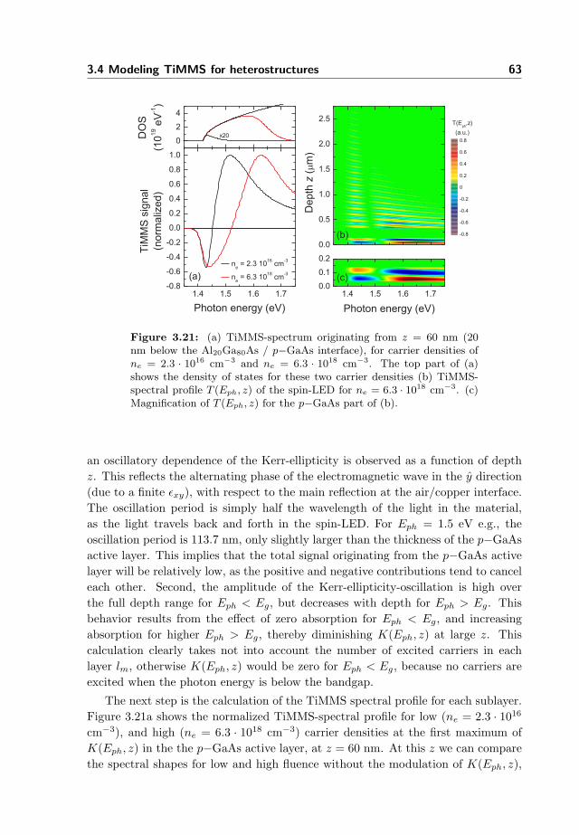
3.4 Modeling TiMMS for heterostructures 63
1.4 1.5 1.6 1.7-0.8
-0.6
-0.4
-0.2
0.0
0.2
0.4
0.6
0.8
1.0
0
2
4
0.0
0.5
1.0
1.5
2.0
2.5T(E
ph,z)
(a.u.)
Depth
z(m
m)
0.8
0.6
0.4
0.2
0
-0.2
-0.4
-0.6
-0.8
1.4 1.5 1.6 1.70.0
0.1
0.2
Photon energy (eV)
ne
= 2.3 1016
cm-3
ne
= 6.3 1018
cm-3
(c)
(b)
Photon energy (eV)
TiM
MS
sig
nal
(norm
aliz
ed)
(a)
DO
S
(10
19
eV
-1)
x20
Figure 3.21: (a) TiMMS-spectrum originating from z = 60 nm (20nm below the Al20Ga80As / p−GaAs interface), for carrier densities ofne = 2.3 · 1016 cm−3 and ne = 6.3 · 1018 cm−3. The top part of (a)shows the density of states for these two carrier densities (b) TiMMS-spectral profile T (Eph, z) of the spin-LED for ne = 6.3 · 1018 cm−3. (c)Magnification of T (Eph, z) for the p−GaAs part of (b).
an oscillatory dependence of the Kerr-ellipticity is observed as a function of depthz. This reflects the alternating phase of the electromagnetic wave in the y direction(due to a finite εxy), with respect to the main reflection at the air/copper interface.The oscillation period is simply half the wavelength of the light in the material,as the light travels back and forth in the spin-LED. For Eph = 1.5 eV e.g., theoscillation period is 113.7 nm, only slightly larger than the thickness of the p−GaAsactive layer. This implies that the total signal originating from the p−GaAs activelayer will be relatively low, as the positive and negative contributions tend to canceleach other. Second, the amplitude of the Kerr-ellipticity-oscillation is high overthe full depth range for Eph < Eg, but decreases with depth for Eph > Eg. Thisbehavior results from the effect of zero absorption for Eph < Eg, and increasingabsorption for higher Eph > Eg, thereby diminishing K(Eph, z) at large z. Thiscalculation clearly takes not into account the number of excited carriers in eachlayer lm, otherwise K(Eph, z) would be zero for Eph < Eg, because no carriers areexcited when the photon energy is below the bandgap.
The next step is the calculation of the TiMMS spectral profile for each sublayer.Figure 3.21a shows the normalized TiMMS-spectral profile for low (ne = 2.3 · 1016
cm−3), and high (ne = 6.3 · 1018 cm−3) carrier densities at the first maximum ofK(Eph, z) in the the p−GaAs active layer, at z = 60 nm. At this z we can comparethe spectral shapes for low and high fluence without the modulation of K(Eph, z),
64 Chapter 3 Magneto-optical techniques
because K(Eph, z) is fairly constant as a function of Eph due to its close proximityto the surface. The low fluence curve shows a negative peak around the band-gap,followed by a higher positive peak, which decreases to zero at higher energies. Thisbehavior follows from the convolution of a Lorentzian curve with the spin polarizeddensity of states in the conduction band. The curve is in qualitative agreementwith the calculation of Koopmans et al. [27], although in that calculation a two-dimensional density of states was used. At high fluence, the zero crossing shifts tohigher energies, which is caused by band-filling due to the higher carrier density (asindicated in the top part of Fig. 3.21a). We note that at this relatively high carrierdensity, several effects take place, which are not included in the model. Besides thealready mentioned band-filling, also absorption bleaching near the bandgap (or shiftof the absorption edge), and band-gap renormalization take place [29]. Absorptionbleaching is the result of band-filling, as the occupied states at the bottom of theconduction band bleach the optical transitions with energies close to the bandgap.The absorption spectrum will thus experience a blue-shift. Band-gap renormaliza-tion is a consequence of many-particle interactions, resulting in screening of electrons(holes), thereby decreasing (increasing) the energy of the conduction (valence) band.The net result is a decrease of the band-gap, and a red-shift of the absorption spec-trum. Both effects thus have opposite effects, which makes it difficult to predict thenet change to the absorption spectrum, and thereby to the TiMMS spectral shape.The TiMMS-spectral shape calculated with the model at all depths z, T (Eph, z),and at ne = 6.3 · 1018 cm−3, is shown in Fig. 3.21b. Here, both the effects of ab-sorption via A(Eph, z), and the depth dependent Kerr-ellipticity via K(Eph, z) areevident. At energies where there is no absorption, the TiMMS-signal is zero, and atenergies with high absorption, the TiMMS-signal decreases significantly at higherz. Also, the sign of the TiMMS-signal oscillates, the same way as K(Eph, z).
With the information of Fig. 3.21, the TiMMS-spectrum originating from thep−GaAs and the buffer layer can be calculated by summing the different spectra atall z within each layer. We performed the calculation for a wide range of carrier den-sities, thereby obtaining the TiMMS-spectrum of the p−GaAs (Tp−GaAs(Eph, ne)),and the buffer layer (Tbuffer(Eph, ne)) as a function of carrier density. In Fig. 3.22we plot Tp−GaAs(Eph, ne), and Tbuffer(Eph, ne) in a two-dimensional graph, andTp−GaAs(Eph), and Tbuffer(Eph), for three different carrier densities. An importantobservation is that the contributions of the p−GaAs and buffer layer are completelydifferent for all carrier densities. Firstly, the maximum amplitude of Tp−GaAs ishigher than that of Tbuffer as a result of absorption. Secondly, Tbuffer shows threepeaks (two positive and one negative) of comparable amplitude for all carrier den-sities, while in the plot of Tp−GaAs only one peak at low carrier density, and two athigh carrier density are observed. This difference originates from the z-dependenceof K(Eph, z), and the summation of contributions for many different z’s. Finally,the position of the zero-crossing between the main positive and negative peak inTp−GaAs shifts to higher energy with increasing carrier density, as a result of band-

3.4 Modeling TiMMS for heterostructures 65
-10
0
10
20
-10
0
10
20
1.4 1.5 1.6 1.70
1
2
3
4
5
6
7
(b)(a)
Photon energy (eV)
Carr
ier
density
ne
(10
18
cm
-3)
24
18
12
6.0
0
-6.0
-12
-18
-24
1.4 1.5 1.6 1.70
1
2
3
4
5
6
7
Photon energy (eV)
Tp
-Ga
As
(Ep
h,n
e)
(a.u
.)
ne
(1018
cm-3
)
0.02
3.85
7.70
ne
(1018
cm-3
)
0.02
3.85
7.70
Tp
-Ga
As
(Ep
h,
ne)
(a.u
.)
Tb
uffe
r(E
ph,
ne)
(a.u
.)
Figure 3.22: (a) Bottom: 2D-plot of the TiMMS-spectrum originat-ing from the p−GaAs layer of the spin-LED as a function of carrierdensity, Tp−GaAs(Eph, ne). Top: Tp−GaAs(Eph) for three different car-rier densities. (b) Bottom: 2D-plot of the TiMMS-spectrum originatingfrom the buffer layer of the spin-LED as a function of carrier density,Tbuffer(Eph, ne). Top: Tbuffer(Eph) for three different carrier densities.
filling effects discussed above.Comparing experimental TiMMS-spectra taken on the spin-LED with the ones
calculated above, enables discrimination between contributions from different layersof the semiconductor heterostructure. Full time- and spectrally-resolved TiMMS-data thus allows us to study the electron spin relaxation mechanisms in the activep−GaAs layer of this spin-LED, which is the topic of Chapter 5.
To conclude, we have outlined an approach for calculating the TiMMS spectralprofiles of arbitrary semiconductor heterostructures. Although a detailed analysis ofthe system in question is necessary, this approach shows that it is possible to extractinformation from different layers from the general complicated TiMMS-spectra. Thisway, studies of spin relaxation mechanisms, transport and diffusion can be extendedfrom model systems to complicated spintronic devices.
66 Chapter 3 Magneto-optical techniques
Bibliography
[1] H. Ebert, Magneto-optical effects in transition metal systems, Rep. Prog. Phys.59 1665-1735 (1996). 3.1.1
[2] F.L. Pedrotti, S.J. and L.S. Pedrotti, Introduction to optics, (Prentice HallInternational Inc., New Jersey, 1996). 3.1.1
[3] B. Koopmans, Laser-induced Magnetization Dynamics, in Topics in AppliedPhysics Vol 87, (Springer: Berlin, 2003), p. 253-320. 3.1.2, 3.1.5, 3.2
[4] N. C. Gerhardt, S. Hovel, C. Brenner, M. R. Hofmann, F.-Y. Lo, D. Reuter, A.D. Wieck, E. Schuster, W. Keune, and K. Westerholt, Electron spin injectioninto GaAs from ferromagnetic contacts in remanence, Appl. Phys. Lett. 87,032502 (2005). 3.1.3
[5] A. Sinsarp, T. Manago, F. Takano, and H. Akinaga, Electrical Spin Injectionfrom Out-of-Plane Magnetized FePt/MgO Tunneling Junction into GaAs atRoom Temperature, Jpn. J. Appl. Phys., Part 2 46, L4 (2006).
[6] S. Hovel,1, N. C. Gerhardt, M. R. Hofmann, F.-Y. Lo, D. Reuter, A. D. Wieck,E. Schuster, W. Keune, H. Wende, O. Petracic, and K. Westerholt, Electricaldetection of photoinduced spins both at room temperature and in remanence,Appl. Phys. Lett. 92, 242102 (2008). 3.1.3
[7] V. F. Motsnyi, V. I. Safarov, J. De Boeck, J. Das, W. Van Roy, E.Goovaerts, and G. Borghs, Electrical spin injection in a ferromagnet/tunnelbarrier/semiconductor heterostructure, Appl. Phys. Lett. 81, 265-267 (2002).3.1.3
[8] P. F. Carcia, A. D. Meinhaldt, and A. Suna, Perpendicular magnetic anisotropyin Pd/Co thin film layered structures, Appl. Phys. Lett. 47, 178 (1985). 3.1.3
[9] H. J. G. Draaisma, W. J. M. de Jonge, and F. J. A. den Broeder, Magneticinterface anisotropy in Pd/Co and Pd/Fe multilayers, J. Magn. Magn. Mater.66, 351-355 (1987).
[10] P. F. Carcia, Perpendicular magnetic anisotropy in Pd/Co and Pt/Co thin-filmlayered structures, J. Appl. Phys. 63, 5066 (1988). 3.1.3, 3.1.5
[11] M. T. Johnson, P. J. H. Bloemen, F. J. A. den Broeder, and J. J. de Vries,Magnetic anisotropy in metallic multilayers, Rep. Prog. Phys. 59 1409-1458(1996). 3.1.3
[12] P. V. Paluskar, J. T. Kohlhepp, H. J. M. Swagten, and B. Koopmans,Co72Fe20B8: Structure, magnetism, and tunneling spin polarization, J. Appl.Phys. 99, 08E503 (2006). 3.1.3
BIBLIOGRAPHY 67
[13] J. Zak, E. R. Moog, C. Liu, and S. D. Bader, Universal approach to magneto-optics, J. Magn. Magn. Mater. 89, 107-123 (1990). 3.1.4, 3.1.4
[14] J. Zak, E. R. Moog, C. Liu, and S. D. Bader, Magneto-optics of multilayerswith arbitrary magnetization directions, Phys. Rev. B 43, 6423-6429 (1991).3.1.4, 3.1.4, 3.1.5
[15] P. Yeh, Optical waves in layered media, (Wiley & Sons, Inc, New York, 1988).3.1.4, 3.4
[16] G. Malinowski, F. Dalla Longa, J. H. H. Rietjens, P. V. Paluskar, R. Huijink,H. J. M Swagten, and B. Koopmans, Control of speed and efficiency of ultrafastdemagnetization by direct transfer of spin angular momentum, Nat. Phys. 4,855 (2008). 3.1.5
[17] J. H. Weaver, and H. P. R. Frederikse, Optical properties of selected elements,in Handbook of Chemistry and Physics, 88th Edition, p. 12-120 - 12-144. 3.1.5,3.4
[18] L. I. Berger, Optical properties of selected inorganica and organic solids, inHandbook of Chemistry and Physics, 88th Edition, p. 12-144 - 12-159. 3.1.5,3.4
[19] R. Atkinson, S. Pahirathan, I. W. Salter, P. J. Grundy, C. J. Tatnall, J. C.Lodder, and Q. Meng, Fundamental optical and magneto-optical constants ofCo/Pt and CoNi/Pt multilayered films, J. Magn. Magn. Mat 162, 131-138(1996). 3.1.5, 3.1.5
[20] C. Jozsa, Optical detection of the magnetization precession - choreography on asub-nanosecond timescale, Pd.D. Thesis, Eindhoven University of Technology,Eindhoven, The Netherlands (2006). 3.2
[21] W. K. Hiebert, A. Stankiewicz, and M. R. Freeman, Direct Observation ofMagnetic Relaxation in a Small Permalloy Disk by Time-Resolved ScanningKerr Microscopy, Phys. Rev. Lett. 79, 1134 (1997) 3.2
[22] B. Koopmans, J. E. M. Haverkort, W. J. M. de Jonge, and G. Karczewski,Time-resolved magnetization modulation spectroscopy: A new probe of ultrafastspin dynamics, J. Appl. Phys. 85, 6763 (1999). 3.3
[23] P. Van Dorpe, R. Vanheertum, H. Boukari, W. Van Roy, and G. Borghs, Designof the tunnel contacts and the transport region of all-electrical spin-injection-detection devices, J. Appl. Phys. 99, 08S702 (2006). 3.12, 3.3.3
[24] J. M. Kikkawa, and D. D. Awschalom, Resonant spin amplification in n-typeGaAs, Phys. Rev. Lett. 80, 4313-4316 (1998). 3.3.3

68 Chapter 3 Magneto-optical techniques
[25] M. E. Flatte , and J. M. Byers, Spin diffusion in semiconductors, Phys. Rev.Lett. 84, 4220-4223 (2000). 3.3.3
[26] S. A. Crooker, and D. L. Smith, Imaging spin flows in semiconductors subjectto electric, magnetic, and strain fields, Phys. Rev. Lett. 94, 236601 (2005).3.3.3
[27] B. Koopmans, and W. J. M. de Jonge, Ultrafast spin dynamics in mag-netic semiconductor quantum wells studied by magnetization modulation spec-troscopy, Appl. Phys. B 68, 525 (1999). 3.4, 3.4, 3.4
[28] S. Adachi, Properties of Aluminium Gallium Arsenide, (London: IEE, 1993).3.4
[29] B. R. Bennett, R. A. Soref, and J. A. Del Alamo, Carrier-Induced Change inRefractive Index of InP, GaAs, and InGaAsP, IEEE J. Quantum Electron. 26,113-122 (1990). 3.4
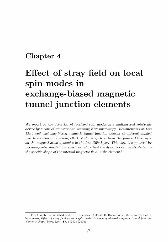
Chapter 4
Effect of stray field on localspin modes inexchange-biased magnetictunnel junction elements
We report on the detection of localized spin modes in a multilayered spintronic
device by means of time-resolved scanning Kerr microscopy. Measurements on this
13×9 µm2 exchange-biased magnetic tunnel junction element at different applied
bias fields indicate a strong effect of the stray field from the pinned CoFe layer
on the magnetization dynamics in the free NiFe layer. This view is supported by
micromagnetic simulations, which also show that the dynamics can be attributed to
the specific shape of the internal magnetic field in the element.1
1This Chapter is published as J. H. H. Rietjens, C. Jozsa, H. Boeve, W. J. M. de Jonge, and B.Koopmans, Effect of stray field on local spin modes in exchange-biased magnetic tunnel junctionelements, Appl. Phys. Lett. 87, 172508 (2005)
69
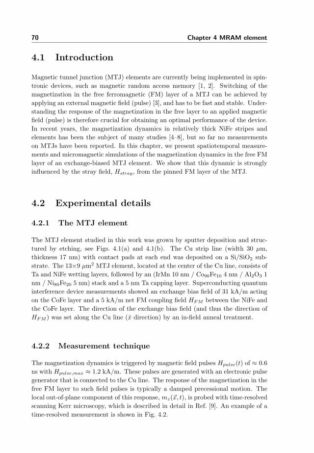
70 Chapter 4 MRAM element
4.1 Introduction
Magnetic tunnel junction (MTJ) elements are currently being implemented in spin-tronic devices, such as magnetic random access memory [1, 2]. Switching of themagnetization in the free ferromagnetic (FM) layer of a MTJ can be achieved byapplying an external magnetic field (pulse) [3], and has to be fast and stable. Under-standing the response of the magnetization in the free layer to an applied magneticfield (pulse) is therefore crucial for obtaining an optimal performance of the device.In recent years, the magnetization dynamics in relatively thick NiFe stripes andelements has been the subject of many studies [4–8], but so far no measurementson MTJs have been reported. In this chapter, we present spatiotemporal measure-ments and micromagnetic simulations of the magnetization dynamics in the free FMlayer of an exchange-biased MTJ element. We show that this dynamic is stronglyinfluenced by the stray field, Hstray, from the pinned FM layer of the MTJ.
4.2 Experimental details
4.2.1 The MTJ element
The MTJ element studied in this work was grown by sputter deposition and struc-tured by etching, see Figs. 4.1(a) and 4.1(b). The Cu strip line (width 30 µm,thickness 17 nm) with contact pads at each end was deposited on a Si/SiO2 sub-strate. The 13×9 µm2 MTJ element, located at the center of the Cu line, consists ofTa and NiFe wetting layers, followed by an (IrMn 10 nm / Co90Fe10 4 nm / Al2O3 1nm / Ni80Fe20 5 nm) stack and a 5 nm Ta capping layer. Superconducting quantuminterference device measurements showed an exchange bias field of 31 kA/m actingon the CoFe layer and a 5 kA/m net FM coupling field HFM between the NiFe andthe CoFe layer. The direction of the exchange bias field (and thus the direction ofHFM ) was set along the Cu line (x direction) by an in-field anneal treatment.
4.2.2 Measurement technique
The magnetization dynamics is triggered by magnetic field pulses Hpulse(t) of ≈ 0.6ns with Hpulse,max ≈ 1.2 kA/m. These pulses are generated with an electronic pulsegenerator that is connected to the Cu line. The response of the magnetization in thefree FM layer to such field pulses is typically a damped precessional motion. Thelocal out-of-plane component of this response, mz(~x, t), is probed with time-resolvedscanning Kerr microscopy, which is described in detail in Ref. [9]. An example of atime-resolved measurement is shown in Fig. 4.2.
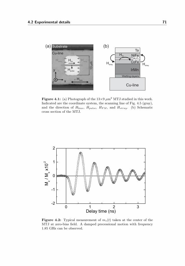
4.2 Experimental details 71
y
z
Hpulse
Hfm
13
mm
Hstray
Cu-line
Wetting-layers
Ta
x
(a) (b)
IrMn
Hbias
Hstray
Hfm
Al O2 3
NiFe
CoFeHstray
Cu-line
Substrate
Hstray
Figure 4.1: (a) Photograph of the 13×9 µm2 MTJ studied in this work.Indicated are the coordinate system, the scanning line of Fig. 4.5 (gray),and the direction of Hbias, Hpulse, HFM , and Hstray. (b) Schematiccross section of the MTJ.
0 1 2 3-2
-1
0
1
2
Mz /
Ms x
10-2
Delay time (ns)
Figure 4.2: Typical measurement of mz(t) taken at the center of theMTJ at zero-bias field. A damped precessional motion with frequency1.85 GHz can be observed.
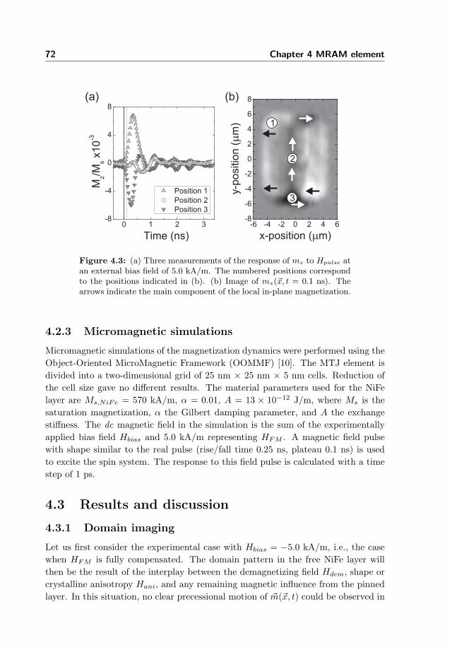
72 Chapter 4 MRAM element
-6 -4 -2 0 2 4 6-8
-6
-4
-2
0
2
4
6
8
x-position (mm)y-p
ositio
n(m
m)
0 1 2 3-8
-4
0
4
8
Mz/M
sx1
0-3
Time (ns)
Position 1
Position 2
Position 3
(a) (b)
1
2
3
Figure 4.3: (a) Three measurements of the response of mz to Hpulse atan external bias field of 5.0 kA/m. The numbered positions correspondto the positions indicated in (b). (b) Image of mz(~x, t = 0.1 ns). Thearrows indicate the main component of the local in-plane magnetization.
4.2.3 Micromagnetic simulations
Micromagnetic simulations of the magnetization dynamics were performed using theObject-Oriented MicroMagnetic Framework (OOMMF) [10]. The MTJ element isdivided into a two-dimensional grid of 25 nm × 25 nm × 5 nm cells. Reduction ofthe cell size gave no different results. The material parameters used for the NiFelayer are Ms,NiFe = 570 kA/m, α = 0.01, A = 13 × 10−12 J/m, where Ms is thesaturation magnetization, α the Gilbert damping parameter, and A the exchangestiffness. The dc magnetic field in the simulation is the sum of the experimentallyapplied bias field Hbias and 5.0 kA/m representing HFM . A magnetic field pulsewith shape similar to the real pulse (rise/fall time 0.25 ns, plateau 0.1 ns) is usedto excite the spin system. The response to this field pulse is calculated with a timestep of 1 ps.
4.3 Results and discussion
4.3.1 Domain imaging
Let us first consider the experimental case with Hbias = −5.0 kA/m, i.e., the casewhen HFM is fully compensated. The domain pattern in the free NiFe layer willthen be the result of the interplay between the demagnetizing field Hdem, shape orcrystalline anisotropy Hani, and any remaining magnetic influence from the pinnedlayer. In this situation, no clear precessional motion of ~m(~x, t) could be observed in
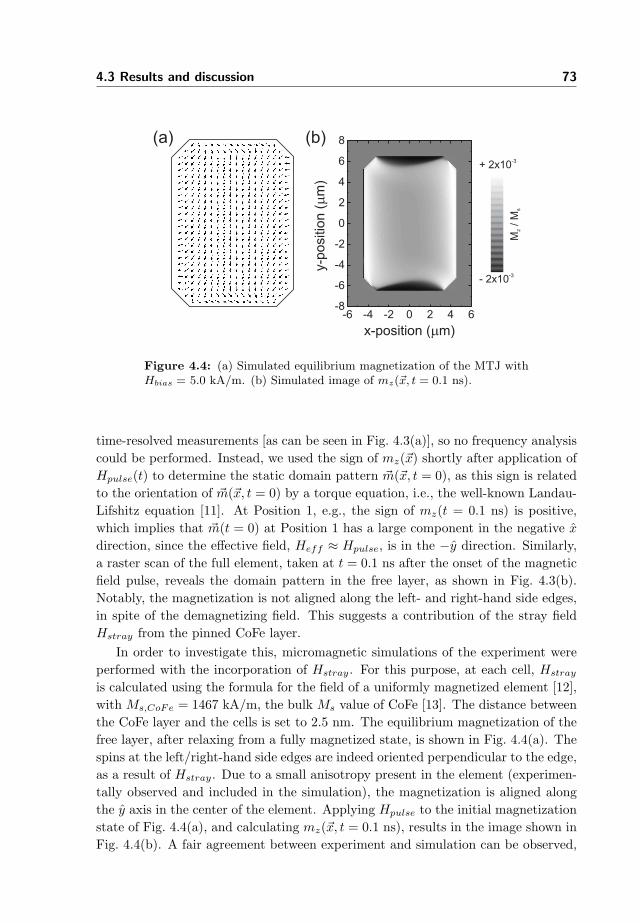
4.3 Results and discussion 73
-6 -4 -2 0 2 4 6-8
-6
-4
-2
0
2
4
6
8
x-position (mm)y-p
ositio
n(m
m)
+ 2x10⁻³
- 2x10⁻³
M/
Mz
s
(a) (b)
Figure 4.4: (a) Simulated equilibrium magnetization of the MTJ withHbias = 5.0 kA/m. (b) Simulated image of mz(~x, t = 0.1 ns).
time-resolved measurements [as can be seen in Fig. 4.3(a)], so no frequency analysiscould be performed. Instead, we used the sign of mz(~x) shortly after application ofHpulse(t) to determine the static domain pattern ~m(~x, t = 0), as this sign is relatedto the orientation of ~m(~x, t = 0) by a torque equation, i.e., the well-known Landau-Lifshitz equation [11]. At Position 1, e.g., the sign of mz(t = 0.1 ns) is positive,which implies that ~m(t = 0) at Position 1 has a large component in the negative x
direction, since the effective field, Heff ≈ Hpulse, is in the −y direction. Similarly,a raster scan of the full element, taken at t = 0.1 ns after the onset of the magneticfield pulse, reveals the domain pattern in the free layer, as shown in Fig. 4.3(b).Notably, the magnetization is not aligned along the left- and right-hand side edges,in spite of the demagnetizing field. This suggests a contribution of the stray fieldHstray from the pinned CoFe layer.
In order to investigate this, micromagnetic simulations of the experiment wereperformed with the incorporation of Hstray. For this purpose, at each cell, Hstray
is calculated using the formula for the field of a uniformly magnetized element [12],with Ms,CoFe = 1467 kA/m, the bulk Ms value of CoFe [13]. The distance betweenthe CoFe layer and the cells is set to 2.5 nm. The equilibrium magnetization of thefree layer, after relaxing from a fully magnetized state, is shown in Fig. 4.4(a). Thespins at the left/right-hand side edges are indeed oriented perpendicular to the edge,as a result of Hstray. Due to a small anisotropy present in the element (experimen-tally observed and included in the simulation), the magnetization is aligned alongthe y axis in the center of the element. Applying Hpulse to the initial magnetizationstate of Fig. 4.4(a), and calculating mz(~x, t = 0.1 ns), results in the image shown inFig. 4.4(b). A fair agreement between experiment and simulation can be observed,
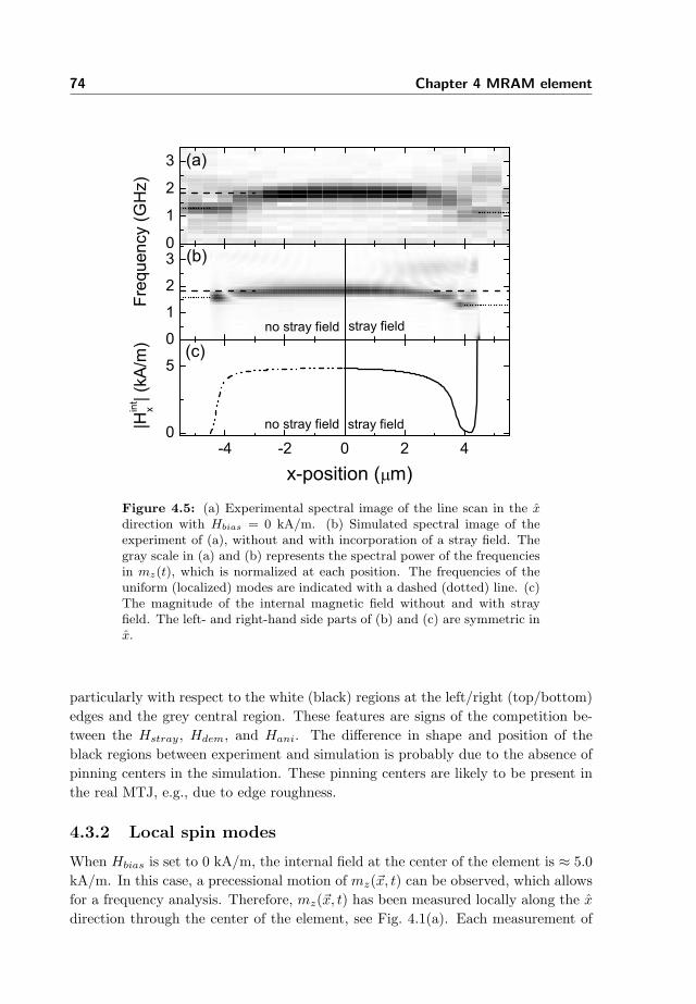
74 Chapter 4 MRAM element
-4 -2 0 2 40
5
0
1
2
3
x-position ( m)
|Hin
tx
| (kA
/m)
Freq
uenc
y (G
Hz)
(c)stray fieldno stray field
stray field
(b)
no stray field
(a)
0
1
2
3
Figure 4.5: (a) Experimental spectral image of the line scan in the xdirection with Hbias = 0 kA/m. (b) Simulated spectral image of theexperiment of (a), without and with incorporation of a stray field. Thegray scale in (a) and (b) represents the spectral power of the frequenciesin mz(t), which is normalized at each position. The frequencies of theuniform (localized) modes are indicated with a dashed (dotted) line. (c)The magnitude of the internal magnetic field without and with strayfield. The left- and right-hand side parts of (b) and (c) are symmetric inx.
particularly with respect to the white (black) regions at the left/right (top/bottom)edges and the grey central region. These features are signs of the competition be-tween the Hstray, Hdem, and Hani. The difference in shape and position of theblack regions between experiment and simulation is probably due to the absence ofpinning centers in the simulation. These pinning centers are likely to be present inthe real MTJ, e.g., due to edge roughness.
4.3.2 Local spin modes
When Hbias is set to 0 kA/m, the internal field at the center of the element is ≈ 5.0kA/m. In this case, a precessional motion of mz(~x, t) can be observed, which allowsfor a frequency analysis. Therefore, mz(~x, t) has been measured locally along the x
direction through the center of the element, see Fig. 4.1(a). Each measurement of
4.3 Results and discussion 75
mz(t) is taken at fixed positions of the laser spot on the sample, in steps of 0.5 µm.The resulting Fourier transformation of mz(~x, t) at each position is shown in Fig.4.5(a). A uniform precessional mode can be observed roughly from −3.5 to +3.5µm, with a frequency, funi, that decreases from 1.85 GHz to 1.76 GHz when movingfrom 0 to ±3.5 µm. At the edges of the element, a localized mode with floc ≈ 1.3GHz can be clearly seen. At +4 µm, a higher-order mode is also observed.
It has been shown [4, 5], that such remarkable localized modes can occur in aregion where the internal magnetic field, Hint, is highly inhomogeneous. Such aregion can arise near the edge of an element due to the demagnetization field, whenan external field [or coupling field (HFM ) as in our experiment] is perpendicularto the edge. Spin waves propagating parallel to this field become confined in apotential well created by the inhomogeneous internal magnetic field, leading to alocalized mode. The frequency of the localized mode depends on the precise shapeof the potential well.
We performed micromagnetic simulations in order to calculate the frequency ofthe localized mode. The result of this simulation, without and with incorporationof Hstray, is shown in Fig. 4.5(b). The frequency of the uniform mode agrees wellwith the experiment in both simulations. However, both the gradual decrease offuni when moving from the center to the edge, and floc agree only in the case whenHstray is included. This can be understood by looking at the internal magneticfield in the element, see Fig. 4.5(c). The steep increase in Hint at ≈ 4.5 µm [Fig.4.5(c) right-hand side part] is due to the strong stray field close to the magneticpole of the CoFe layer. The gradual decrease of Hint between 0 and 3 µm is alsodue to the contribution of the stray field and results in the gradual decrease funi.Furthermore, Hint clearly behaves differently in the region where the localized modeis present, which results in a different shape of the potential well and a ≈ 0.3 GHzlower frequency of the localized mode. Around +4 µm, the simulated spectrumshows multiple peaks that do not correspond directly to the ones observed in theexperiment. This fact, and the lack of symmetry in the experimental data (thereis a 0.15 GHz difference between floc at the left- and right-hand side edge of theelement) in contrast to the simulations, can be attributed to a slight difference inthe internal magnetic field near the edges, as a result of sample imperfections.
We also measured and simulated funi and floc at different bias fields, as presentedin Fig. 4.6. A good agreement between experiment, simulation, and theory can beobserved for the uniform mode, which depends on Hbias according to
funi = γµ0
√(Hbias + HFM )(Hbias + HFM + Ms) (4.1)
where γ is the gyromagnetic ratio and µ0 is the magnetic permeability of vacuum.The dependence of floc on Hbias is similar to the one in the experimental case, buttheir absolute values are on average ≈ 0.16 GHz higher. This difference is compara-ble to the differences attributed to sample imperfections, so a satisfactory agreementbetween experiment and simulation is found when the stray field is included. More-
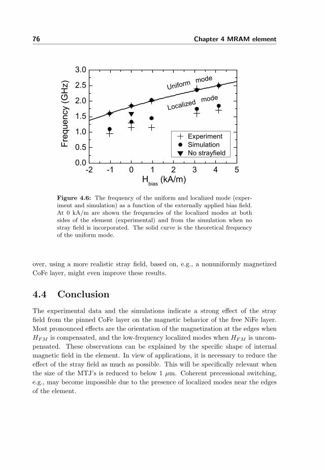
76 Chapter 4 MRAM element
-2 -1 0 1 2 3 4 50.0
0.5
1.0
1.5
2.0
2.5
3.0
Fr
eque
ncy
(GH
z)
ExperimentSimulationNo strayfield
Hbias (kA/m)
mode
modeLocalized
Uniform
Figure 4.6: The frequency of the uniform and localized mode (exper-iment and simulation) as a function of the externally applied bias field.At 0 kA/m are shown the frequencies of the localized modes at bothsides of the element (experimental) and from the simulation when nostray field is incorporated. The solid curve is the theoretical frequencyof the uniform mode.
over, using a more realistic stray field, based on, e.g., a nonuniformly magnetizedCoFe layer, might even improve these results.
4.4 Conclusion
The experimental data and the simulations indicate a strong effect of the strayfield from the pinned CoFe layer on the magnetic behavior of the free NiFe layer.Most pronounced effects are the orientation of the magnetization at the edges whenHFM is compensated, and the low-frequency localized modes when HFM is uncom-pensated. These observations can be explained by the specific shape of internalmagnetic field in the element. In view of applications, it is necessary to reduce theeffect of the stray field as much as possible. This will be specifically relevant whenthe size of the MTJ’s is reduced to below 1 µm. Coherent precessional switching,e.g., may become impossible due to the presence of localized modes near the edgesof the element.

BIBLIOGRAPHY 77
Bibliography
[1] S. A. Wolf, D. D. Awschalom, R. A. Buhrman, J. M. Daughton, S. von Molnar,M. L. Roukes, A. Y. Chtchelkanova, and D. M. Treger, Spintronics: A spin-based electronics vision for the future, Science 294, 1488-1495 (2001). 4.1
[2] B. N. Engel, J. Akerman, B. Butcher, R. W. Dave, M. DeHerrera, M. Durlam,G. Grynkewich, J. Janesky, S. V. Pietambaram, N. D. Rizzo, J. M. Slaughter,K. Smith, J. J. Sun, and S. Tehrani, A 4-Mb toggle MRAM based on a novelbit and switching method, IEEE Trans. Magn. 41, 132 (2005). 4.1
[3] H. W. Schumacher, C. Chappert, R. C. Sousa, P. P. Freitas, and J. Miltat,Quasiballistic magnetization reversal, Phys. Rev. Lett. 90, 017204 (2003). 4.1
[4] J. Jorzick, S. O. Demokritov, B. Hillebrands, M. Bailleul, C. Fermon, K. Y.Guslienko, A. N. Slavin, D. V. Berkov, and N. L. Gorn, Spin Wave Wellsin Nonellipsoidal Micrometer Size Magnetic Elements, Phys. Rev. Lett. 88,047204 (2002). 4.1, 4.3.2
[5] J. P. Park, P. Eames, D. M. Engebretson, J. Berezovksy, and P. A. Crowell,Spatially Resolved Dynamics of Localized Spin-Wave Modes in FerromagneticWires, Phys. Rev. Lett. 89, 277201 (2002). 4.3.2
[6] A. Barman, V. V. Kruglyak, R. J. Hicken, and J. M. Rowe, Imaging the de-phasing of spin wave modes in a square thin film magnetic element, Phys. Rev.B 69, 174426 (2004).
[7] M. Buess, R. Hollinger, T. Haug, K. Perzlmaier, U. Krey, D. Pescia, M. R.Scheinfrein, D. Weiss, and C. H. Back, Fourier Transform Imaging of SpinVortex Eigenmodes, Phys. Rev. Lett. 93, 077207 (2004).
[8] K. Perzlmaier, M. Buess, C. H. Back, V. E. Edimov, B. Hillebrands, and S.O. Demokritov, Spin-Wave Eigenmodes of Permalloy Squares with a ClosureDomain Structure, Phys. Rev. Lett. 94, 057202 (2005). 4.1
[9] J. H. H. Rietjens, C. Jozsa, H. Boeve, W. J. M. de Jonge, and B. Koopmans,Probing local spin modes in exchange-biased MTJ elements, J. Magn. Magn.Mater. 290, 494-497 (2005). 4.2.2
[10] M. J. Donahue and D. G. Porter, OOMMF User’s Guide, version 1.0, Intera-gency Report NISTIR 6376, NIST <http://math.nist.gov/oommf>. 4.2.3
[11] L. Landau and E. Lifshitz, On the theory of the dispersion of magnetic perme-ability in ferromagnetic bodies, Phys. Z. Sowjetunion 8, 153 (1953). 4.3.1
[12] J. D. Jackson, Classical Electrodynamics, 3rd ed. (Wiley, New York, 1999), p.196-197. 4.3.1
78 Chapter 4 MRAM element
[13] Landolt-Bornstein, Group III Condensed Matter (Springer, Berlin, 1986), Vol.19a, p. 189. 4.3.1
Chapter 5
Current-induced increase ofthe electron spin relaxationrate in a spin-LED
A microscopic time-resolved magneto-optical technique is used to investigate in de-
tail the electron spin relaxation rate in a spin-LED under operational conditions.
We have observed a current-induced decrease of the spin lifetime in the active re-
gion of the device, which scales linearly with the current and laser fluence. Device
simulations and spectral measurements show that the main origin for this effect is
an enhanced Bir-Aronov-Pikus (BAP) electron-hole spin flip scattering via an in-
creased hole density and temperature in the active layer. We discuss the role of
carrier recombination, and show that the effect persists outside the spin-LED, and
scales roughly with the current and temperature distribution in the device.1
1A large part of this Chapter is in preparation for publication as J. H. H. Rietjens, C. A. C.Bosco, P. Van Dorpe, W. Van Roy, and B. Koopmans, Current-induced increase of the electronspin relaxation rate in a spin-LED
79
80 Chapter 5 Spin-LED
5.1 Introduction
Injection of spin-polarized electrons into semiconductors and their subsequent ma-nipulation are essential ingredients for realizing functional semiconductor basedspintronic devices [1]. One of the fundamental parameters influencing the devicecharacteristics and efficiency is the spin relaxation time, τs. While most studies ofτs have been performed on bulk or quantum semiconductor systems [2–8], detailedcharacterization of τs in the active part of real devices has received little attentionso far. With the advance of spintronic devices, however, it has become of extremerelevance to understand the spin dynamics under variable operational conditions.
In this chapter, we study the spin relaxation rate of electrons in the active partof a spin-LED under operational conditions. We have performed detailed spectrallyand spatially resolved experiments as a function of applied bias, laser fluence, andtemperature. We have observed an enhanced spin relaxation rate, τs, of electrons ata current of 133 mA, which scales linearly with the injected current. We show thatthe main mechanism for this effect is an enhanced Bir-Aronov-Pikus electron-holespin flip scattering as a result of an increased hole density and temperature in theactive layer. This picture is supported by device simulations, which show that theincreased hole density results from a band re-alignment in the device. Furthermorewe discuss the role of laser photon energy, carrier recombination, and temperatureon the observed effect. Finally, we show by detailed spatial scans that the enhancedspin relaxation rate persists outside the optical window, and scales roughly with acombined current and temperature distribution in the device.
5.2 Experimental details
5.2.1 Measurement technique
We have exploited a microscopic magneto-optical pump-probe technique, Time-resolved Magnetization Modulation Spectroscopy (TiMMS) (see Section 3.3) andRefs. [9] and [10]), to study the electron spin relaxation in the active region of aspin-LED. This technique measures the spin lifetime Ts, which is related to τs andthe carrier recombination time τr via
T−1s = τ−1
s + τ−1r . (5.1)
In short, a circularly polarized pump pulse from a Ti:Sapphire laser (150 fs dura-tion, 80 MHz repetition rate) is focused in the spin-LED (spot diameter ≈ 9 µm)and excites electron spins in the active region. A second, weaker probe beam isfocused to an overlapping spot with a diameter of ≈ 4 µm, and probes the spindynamics through the magneto-optical Kerr-effect. Due to the smaller spotsize ofthe probe compared to the pump, possible complications resulting from a spatiallyinhomogeneous carrier density are reduced. The relative time delay between pump
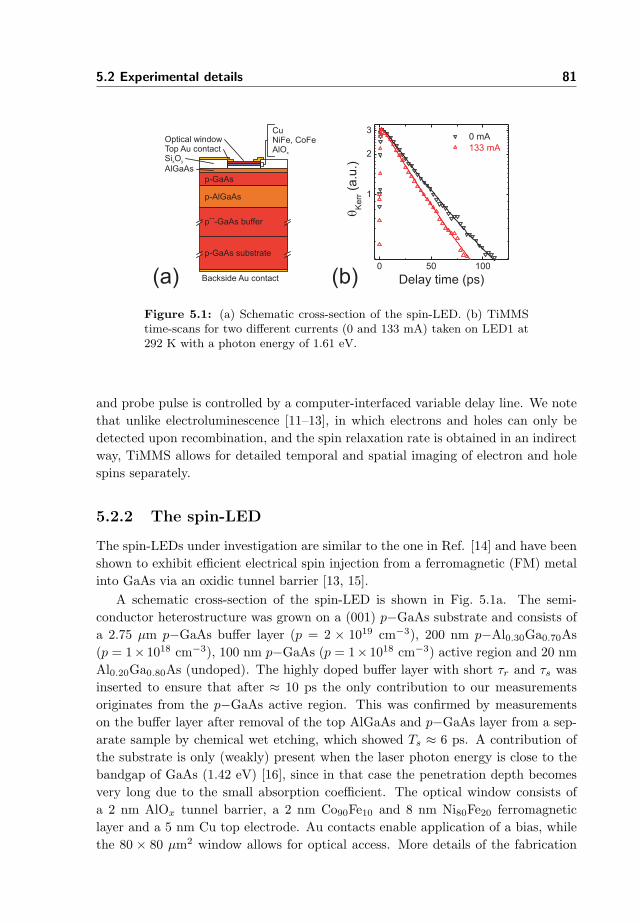
5.2 Experimental details 81
p-GaAs substrate
p -GaAs buffer++
p-AlGaAs
p-GaAs
Backside Au contact
Optical windowTop Au contactSi O
AlGaAsx y
CuNiFe, CoFeAlOx
(a) (b)0 50 100
1
2
30 mA
133 mA
qK
err
(a.u
.)
Delay time (ps)
Figure 5.1: (a) Schematic cross-section of the spin-LED. (b) TiMMStime-scans for two different currents (0 and 133 mA) taken on LED1 at292 K with a photon energy of 1.61 eV.
and probe pulse is controlled by a computer-interfaced variable delay line. We notethat unlike electroluminescence [11–13], in which electrons and holes can only bedetected upon recombination, and the spin relaxation rate is obtained in an indirectway, TiMMS allows for detailed temporal and spatial imaging of electron and holespins separately.
5.2.2 The spin-LED
The spin-LEDs under investigation are similar to the one in Ref. [14] and have beenshown to exhibit efficient electrical spin injection from a ferromagnetic (FM) metalinto GaAs via an oxidic tunnel barrier [13, 15].
A schematic cross-section of the spin-LED is shown in Fig. 5.1a. The semi-conductor heterostructure was grown on a (001) p−GaAs substrate and consists ofa 2.75 µm p−GaAs buffer layer (p = 2 × 1019 cm−3), 200 nm p−Al0.30Ga0.70As(p = 1× 1018 cm−3), 100 nm p−GaAs (p = 1× 1018 cm−3) active region and 20 nmAl0.20Ga0.80As (undoped). The highly doped buffer layer with short τr and τs wasinserted to ensure that after ≈ 10 ps the only contribution to our measurementsoriginates from the p−GaAs active region. This was confirmed by measurementson the buffer layer after removal of the top AlGaAs and p−GaAs layer from a sep-arate sample by chemical wet etching, which showed Ts ≈ 6 ps. A contribution ofthe substrate is only (weakly) present when the laser photon energy is close to thebandgap of GaAs (1.42 eV) [16], since in that case the penetration depth becomesvery long due to the small absorption coefficient. The optical window consists ofa 2 nm AlOx tunnel barrier, a 2 nm Co90Fe10 and 8 nm Ni80Fe20 ferromagneticlayer and a 5 nm Cu top electrode. Au contacts enable application of a bias, whilethe 80 × 80 µm2 window allows for optical access. More details of the fabrication
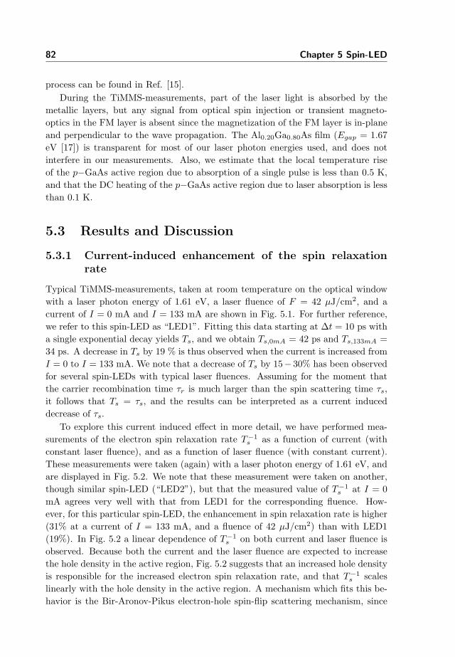
82 Chapter 5 Spin-LED
process can be found in Ref. [15].During the TiMMS-measurements, part of the laser light is absorbed by the
metallic layers, but any signal from optical spin injection or transient magneto-optics in the FM layer is absent since the magnetization of the FM layer is in-planeand perpendicular to the wave propagation. The Al0.20Ga0.80As film (Egap = 1.67eV [17]) is transparent for most of our laser photon energies used, and does notinterfere in our measurements. Also, we estimate that the local temperature riseof the p−GaAs active region due to absorption of a single pulse is less than 0.5 K,and that the DC heating of the p−GaAs active region due to laser absorption is lessthan 0.1 K.
5.3 Results and Discussion
5.3.1 Current-induced enhancement of the spin relaxationrate
Typical TiMMS-measurements, taken at room temperature on the optical windowwith a laser photon energy of 1.61 eV, a laser fluence of F = 42 µJ/cm2, and acurrent of I = 0 mA and I = 133 mA are shown in Fig. 5.1. For further reference,we refer to this spin-LED as “LED1”. Fitting this data starting at ∆t = 10 ps witha single exponential decay yields Ts, and we obtain Ts,0mA = 42 ps and Ts,133mA =34 ps. A decrease in Ts by 19 % is thus observed when the current is increased fromI = 0 to I = 133 mA. We note that a decrease of Ts by 15− 30% has been observedfor several spin-LEDs with typical laser fluences. Assuming for the moment thatthe carrier recombination time τr is much larger than the spin scattering time τs,it follows that Ts = τs, and the results can be interpreted as a current induceddecrease of τs.
To explore this current induced effect in more detail, we have performed mea-surements of the electron spin relaxation rate T−1
s as a function of current (withconstant laser fluence), and as a function of laser fluence (with constant current).These measurements were taken (again) with a laser photon energy of 1.61 eV, andare displayed in Fig. 5.2. We note that these measurement were taken on another,though similar spin-LED (“LED2”), but that the measured value of T−1
s at I = 0mA agrees very well with that from LED1 for the corresponding fluence. How-ever, for this particular spin-LED, the enhancement in spin relaxation rate is higher(31% at a current of I = 133 mA, and a fluence of 42 µJ/cm2) than with LED1(19%). In Fig. 5.2 a linear dependence of T−1
s on both current and laser fluence isobserved. Because both the current and the laser fluence are expected to increasethe hole density in the active region, Fig. 5.2 suggests that an increased hole densityis responsible for the increased electron spin relaxation rate, and that T−1
s scaleslinearly with the hole density in the active region. A mechanism which fits this be-havior is the Bir-Aronov-Pikus electron-hole spin-flip scattering mechanism, since
5.3 Results and Discussion 83
0 40 80 1200.00
0.01
0.02
0.03
0.04
0.05 (b)
T-1 s (p
s-1)
Current (mA)
(a)
0 20 40 60 80 1000.00
0.01
0.02
0.03
0.04
0.05
140 mA 0 mA
T-1 s (p
s-1)
Fluence ( J/cm2)
Figure 5.2: (a) Current dependence of the electron spin relaxation ratein the active region of LED2, taken at a laser fluence of 64 µJ/cm2. (b)Laser-fluence dependence of the electron spin relaxation rate in the sameregion at current of 0 mA (5) and 140 mA (4). All data is taken atroom temperature with a laser photon energy of 1.61 eV.
for this mechanism the spin relaxation rate scales linearly with the hole density fornon-degenerate holes [3].
A simple model to correlate the current and fluence dependence
We can apply a simple model to estimate the increase in hole density in the activeregion of the spin-LED under operational and experimental conditions. Assuminga homogeneous electron and hole density (flat bands), and a linear increase of τ−1
s
with the hole density in the active region (only a BAP-contribution to the electronspin relaxation), it follows that
T−1s ≈ τ−1
s = (τs,0p0)−1 (p0 + pI(I) + pF (F ))
≈ (τs,0p0)−1
(p0 + I
dpI(I)dI
+ FdpF (F )
dF
)(5.2)
where p0 is the intrinsic hole density due to doping (1× 1018 cm−3), pI and pF arethe electrically and optically injected hole densities, respectively, I is the current,and F is the laser fluence. Without bias (V = 0 V, I = 0 mA) and laser fluence(F = 0), we extract from Fig. 5.2b τ−1
s,0 = 0.0144 ps−1 (τs,0 = 70 ps). Using a linearfit of the data of Fig. 5.2a , and 5.2b, we find
84 Chapter 5 Spin-LED
dpI(I)dI ≈ 4.9p0 A−1, and dpF (F )
dF ≈ 0.015p0 cm2µJ−1,
respectively. We can compare these values with an estimation of the injected current-and laser-induced hole densities from experimental parameters:
dpI(I)dI ≈ τr
Ad , and dpF (F )dF ≈ fabs
~ωd .
Here, A is the surface area of the spin-LED, d is the thickness of the active region,fabs is the fraction of the fluence that is absorbed in the active region, and ~ω is thelaser photon energy. We assume that the induced hole density is equal to the inducedelectron density, which is certainly true for optical injection, but is less trivial forelectrical injection because of possible hole tunneling from the semiconductor to theFM layer. With ~ω = 1.61 eV we calculated fabs = 0.044, and using τr = 273 ps,we find
dpI(I)dI ≈ 2.7p0 A−1 and dpF (F )
dF ≈ 0.017p0 cm2µJ−1.
We observe a fair agreement for dpF /dF with our simple model, which supports ourassumption that the BAP-mechanism is responsible for the enhanced spin relaxationrate via an increased hole density. We shall discuss the somewhat higher discrepancyfor dpI/dp and our choice for the recombination time in due course. In this analysiswe neglected the fact that the slopes in Fig. 5.2b at I = 0 mA and I = 140mA are slightly different. This indicates a stronger fluence dependence of T−1
s athigher current, and a weaker current dependence of T−1
s at high fluence. We notethat the relative current induced contribution to T−1
s is highest at zero fluence, i.e.extrapolating the results of Fig. 5.2b to zero fluence yields a current induced effectof 40% at 140 mA.
Device simulation
In order to explore the physical picture of the enhanced electron spin relaxationrate in more detail, we performed simulations of the band alignment and the carrierprofile in the spin-LED using the MEDICI software package [18] (see the Appendixfor a comparison of the experimentally and simulated current-voltage characteris-tics). Figure 5.3 shows the band diagram, and carrier profiles at 0 V and 2.4 V(corresponding to I = 0 mA, and I = 163 mA). At zero bias, band bending near thep−GaAs/Al0.20Ga0.80As interface results in a sharp drop of the hole concentrationnear this interface, and in a strong local electric field. Optically injected electronswill reside near the p−GaAs/Al0.20Ga0.80As interface, and experience a low spin-flip scattering with holes due to the low local hole concentration. For high bias,the active region is pulled flat, and the hole concentration increases from 8.6× 10¹⁷
cm−3 to approximately 9.8×1017 cm−3 throughout the whole device. This increaseresults mainly from an increase in electron density (1× 1017 cm−3) in the active re-gion, where the additional hole density ensures charge neutrality. Since the electrons
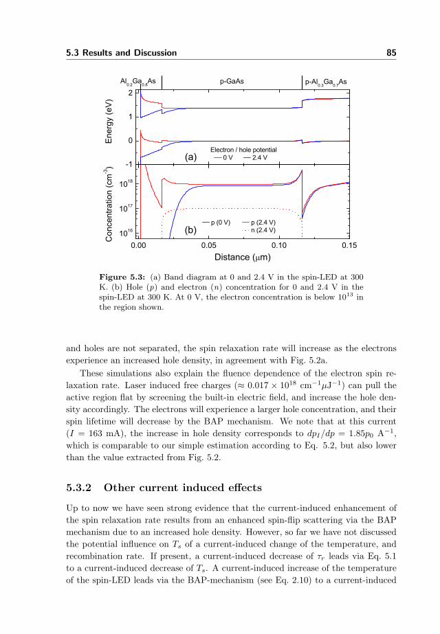
5.3 Results and Discussion 85
0.00 0.05 0.10 0.151016
1017
1018
p (0 V) p (2.4 V) n (2.4 V)
Con
cent
ratio
n (c
m-3)
Distance ( m)
-1
0
1
2
Electron / hole potential 0 V 2.4 V
(b)
Ene
rgy
(eV
)
(a)
Al0.2
Ga0.8
As p-GaAs p-Al0.3
Ga0.7
As
Figure 5.3: (a) Band diagram at 0 and 2.4 V in the spin-LED at 300K. (b) Hole (p) and electron (n) concentration for 0 and 2.4 V in thespin-LED at 300 K. At 0 V, the electron concentration is below 1013 inthe region shown.
and holes are not separated, the spin relaxation rate will increase as the electronsexperience an increased hole density, in agreement with Fig. 5.2a.
These simulations also explain the fluence dependence of the electron spin re-laxation rate. Laser induced free charges (≈ 0.017 × 1018 cm−1µJ−1) can pull theactive region flat by screening the built-in electric field, and increase the hole den-sity accordingly. The electrons will experience a larger hole concentration, and theirspin lifetime will decrease by the BAP mechanism. We note that at this current(I = 163 mA), the increase in hole density corresponds to dpI/dp = 1.85p0 A−1,which is comparable to our simple estimation according to Eq. 5.2, but also lowerthan the value extracted from Fig. 5.2.
5.3.2 Other current induced effects
Up to now we have seen strong evidence that the current-induced enhancement ofthe spin relaxation rate results from an enhanced spin-flip scattering via the BAPmechanism due to an increased hole density. However, so far we have not discussedthe potential influence on Ts of a current-induced change of the temperature, andrecombination rate. If present, a current-induced decrease of τr leads via Eq. 5.1to a current-induced decrease of Ts. A current-induced increase of the temperatureof the spin-LED leads via the BAP-mechanism (see Eq. 2.10) to a current-induced

86 Chapter 5 Spin-LED
decrease of τs. According to Fig. 5.10b the dissipated power in the spin-LED is onlyweakly non-linear. As the increase in temperature scales linearly with the dissipatedpower, the signature of a current-induced temperature rise might be similar to thatof a current-induced hole density.
In this Section we will discuss the role of recombination, and temperature inmore detail. It will become clear that the BAP-mechanism also reduces the spinrelaxation time via a temperature increase, and that only part of the current induceddecrease of Ts can be attributed to a non-constant carrier recombination rate. Westart with discussing spectral measurements of the current-induced effect.
Spectroscopic TiMMS data
The TiMMS-data presented so far have all been taken at a laser photon energyof 1.61 eV. Results from spectroscopic measurements, with laser photon energiesbetween 1.47 and 1.69 eV, and taken at a current of both 0 mA and 133 mA,are presented in Fig. 5.4. We see that Ts depends strongly on the laser photonenergy, when using a single exponential fit to the data starting at ∆t = 10 ps. Thedivergence of Ts is related to a zero crossing of the amplitude of the TiMMS-signal,see Fig. 5.4(b), which displays the amplitude of the TiMMS-signal at ∆t = 5 ps.The position of this zero crossing is very sensitive to the carrier density in the device,and therefore time-dependent in our experiment due to carrier recombination.
We performed simulations of the TiMMS-time traces versus photon energy fol-lowing the approach of Koopmans et al. [10] taking into account this time-dependentzero-crossing, the absorption profile, and depth dependence of the magneto-opticalKerr-effect [19] (discussed in detail in Sections 3.1.4 and 3.4). The simulated time-traces are also fitted with a single exponential decay in order to extract Ts,sim,yielding the lines shown in Fig. 5.4. Using τs = 41 ps, and τr = 390 ps, we cannicely match the experimental data at I = 0 mA. The range in τs and τr whichgive a reasonable match are (τs = 39 ps, τr = 480 ps) to (τs = 43 ps, τr = 300ps). In order to simulate the data at I = 133 mA, we have to take into account adecrease in τs and/or a decrease in τr, and also a spectral redshift of the TiMMSspectrum of 7.5 meV. This redshift is experimentally observed (see Fig. 5.4b), andis attributed to a shift of the band-gap due to current-induced heating of the device.The data at I = 133 mA is simulated for the cases of a decrease of (i) only τr (ii)only τs, and (iii) both τs and τr, as shown in Fig. 5.4. In each case, values for ∆τr
and ∆τs are chosen such that ∆Ts is consistent with the experimental data at lowand high photon energy. We see that the data can only be well matched at everyphoton energy if a decrease of τs is taken into account, but also that a decreasein τr cannot be excluded. We note that direct measurements of τr are in princi-ple possible by measuring the carrier dynamics in the active layer via the transientreflectivity. However, the interpretation of such measurements performed on theoptical window of the spin-LED proved less trivial. Due to complications related tothe semiconductor heterostructure, such as contributions from other layers, heating
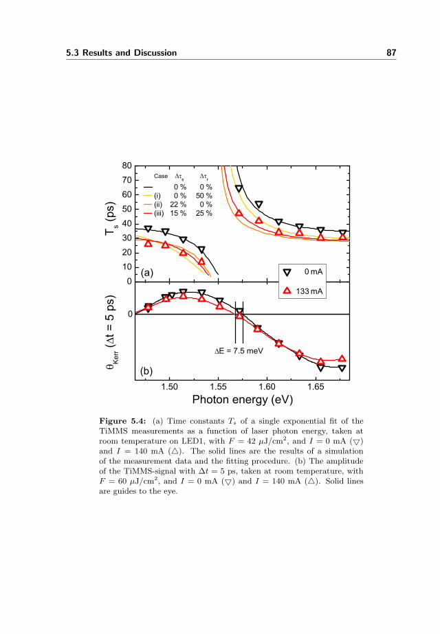
5.3 Results and Discussion 87
01020304050607080
1.50 1.55 1.60 1.65
0
0 mA
133 mA
Case s r
0 % 0 % (i) 0 % 50 % (ii) 22 % 0 % (iii) 15 % 25 %
(b)
T s (ps)
(a)
Ker
r (t =
5 p
s)
Photon energy (eV)
E = 7.5 meV
Figure 5.4: (a) Time constants Ts of a single exponential fit of theTiMMS measurements as a function of laser photon energy, taken atroom temperature on LED1, with F = 42 µJ/cm2, and I = 0 mA (5)and I = 140 mA (4). The solid lines are the results of a simulationof the measurement data and the fitting procedure. (b) The amplitudeof the TiMMS-signal with ∆t = 5 ps, taken at room temperature, withF = 60 µJ/cm2, and I = 0 mA (5) and I = 140 mA (4). Solid linesare guides to the eye.
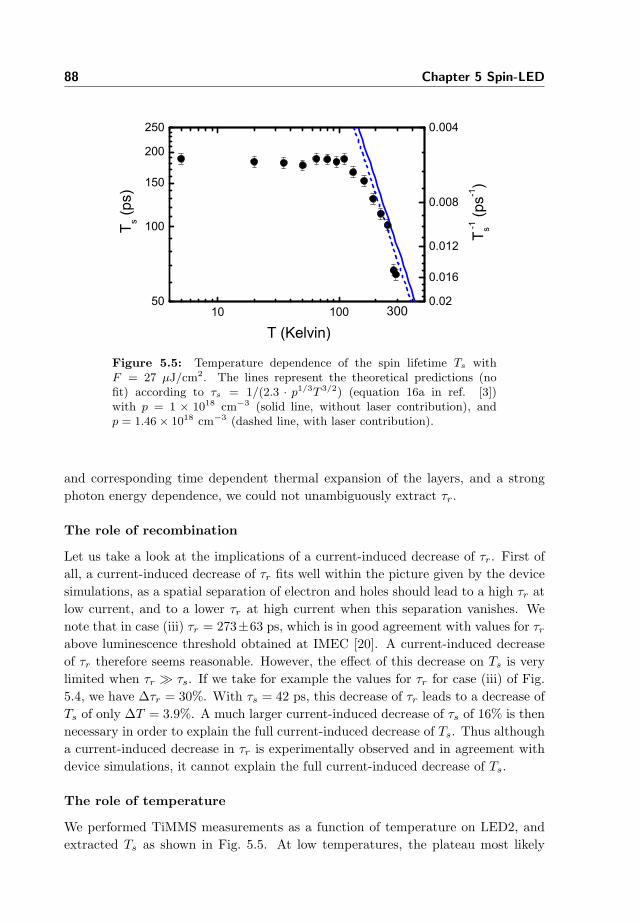
88 Chapter 5 Spin-LED
10 10050
100
150
200
250
0.02
0.016
0.012
0.008
0.004
T s (
ps)
T (Kelvin)300
T -1 s
(ps-1
)
Figure 5.5: Temperature dependence of the spin lifetime Ts withF = 27 µJ/cm2. The lines represent the theoretical predictions (nofit) according to τs = 1/(2.3 · p1/3T 3/2) (equation 16a in ref. [3])with p = 1 × 1018 cm−3 (solid line, without laser contribution), andp = 1.46× 1018 cm−3 (dashed line, with laser contribution).
and corresponding time dependent thermal expansion of the layers, and a strongphoton energy dependence, we could not unambiguously extract τr.
The role of recombination
Let us take a look at the implications of a current-induced decrease of τr. First ofall, a current-induced decrease of τr fits well within the picture given by the devicesimulations, as a spatial separation of electron and holes should lead to a high τr atlow current, and to a lower τr at high current when this separation vanishes. Wenote that in case (iii) τr = 273±63 ps, which is in good agreement with values for τr
above luminescence threshold obtained at IMEC [20]. A current-induced decreaseof τr therefore seems reasonable. However, the effect of this decrease on Ts is verylimited when τr À τs. If we take for example the values for τr for case (iii) of Fig.5.4, we have ∆τr = 30%. With τs = 42 ps, this decrease of τr leads to a decrease ofTs of only ∆T = 3.9%. A much larger current-induced decrease of τs of 16% is thennecessary in order to explain the full current-induced decrease of Ts. Thus althougha current-induced decrease in τr is experimentally observed and in agreement withdevice simulations, it cannot explain the full current-induced decrease of Ts.
The role of temperature
We performed TiMMS measurements as a function of temperature on LED2, andextracted Ts as shown in Fig. 5.5. At low temperatures, the plateau most likely
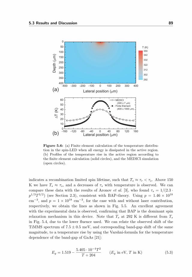
5.3 Results and Discussion 89
-160 -120 -80 -40 0 40 80 120 1600
10
20
30
40
50
60 MEDICI
(300 x 7 mm)
Finite Element
(400 x 1000 mm)
DT
(K)
Lateral position (mm)
-400 -300 -200 -100 0 100 200 300 400400
350
300
250
200
150
100
50
0
Lateral position (mm)
De
pth
(mm
)
292
302
312
322
332
342
350
T (K)
(a)
(b)
Figure 5.6: (a) Finite element calculation of the temperature distribu-tion in the spin-LED when all energy is dissipated in the active region.(b) Profiles of the temperature rise in the active region according tothe finite element calculation (solid circles), and the MEDICI simulation(open circles).
indicates a recombination limited spin lifetime, such that Ts ≈ τr < τs. Above 150K we have Ts ≈ τs, and a decreases of τs with temperature is observed. We cancompare these data with the results of Aronov et al. [3], who found τs = 1/(2.3 ·p1/3T 3/2) (see Section 2.3), consistent with BAP-theory. Using p = 1.46 × 10¹⁸
cm−3, and p = 1 × 1018 cm−3, for the case with and without laser contribution,respectively, we obtain the lines as shown in Fig. 5.5. An excellent agreementwith the experimental data is observed, confirming that BAP is the dominant spinrelaxation mechanism in this device. Note that Ts at 292 K is different from Ts
in Fig. 5.4, due to the lower fluence used. We can relate the observed shift of theTiMMS spectrum of 7.5 ± 0.5 meV, and corresponding band-gap shift of the samemagnitude, to a temperature rise by using the Varshni-formula for the temperaturedependence of the band-gap of GaAs [21]:
Eg = 1.519− 5.405 · 10−4T 2
T + 204(Eg in eV, T in K) (5.3)
90 Chapter 5 Spin-LED
With ∆Eg = 7.5± 0.5 meV, Eq. 5.3 yields ∆T = 17± 1 K.We can compare this ∆T with the results of the MEDICI-simulation (300 µm × 7
µm 2D-grid), and a simple finite element calculation (FEC) (cylindrical 2 mm × 400µm quasi 3D-grid), of the temperature distribution in the spin-LED. In the FEC itis assumed that all electrical energy (P = 0.32 W with V = 2.4 V, and I = 0.133 A)is dissipated in the active layer under the optical window in the semiconductor. Theboundary condition for the back-contact is T = 292 K, whereas all other boundarieshave Neumann-conditions with no heat transfer. Therefore, the calculated ∆T
can be regarded as an upper limit for the current-induced temperature rise. Thevalues for the thermal conductivity of each layer were taken from literature [16, 17].We used a cylindrical geometry and calculated the equilibrium temperature on anappropriate mesh of height 0.4 mm and radius 1 mm. The result is shown in Fig. 5.6,from which a maximum temperature rise under the optical window of several tens ofKelvin is observed. The differences between the MEDICI and the FEC calculationmost likely originate from the different grid sizes used. These simulations indicatethat experimentally observed temperature rise of ≈ 17 K is reasonable. Accordingto Fig. 5.5, the increase in temperature of ∆T ≈ 17 K corresponds to a decrease ofTs of ≈ 8%. From this observation we conclude that a current-induced temperaturerise also contributes to the decrease of Ts, however, it is too small to account forthe full observed effect.
We now return to the apparent discrepancy between the measured dpI/dp usingour simple model and the estimation from experimental parameters. From Fig. 5.4we have observed that the current-induced decrease of Ts is best described by acurrent-induced decrease of τs somewhere between 15% (case (iii)) and 22% (case(ii)). Of this 15− 22%, we have seen that ≈ 8% is due to the temperature rise. Theestimation of dpI/dp should thus also include the effect of temperature, which yields4.2p0 < dpI/dp < 5.7p0. Now a good agreement with the simple model is observed.Summarizing, the observed current-induced decrease of Ts is mainly caused by adecrease of τs, and partly due to the effect of a reduced τr. The current-induceddecrease of τs is mediated by the BAP-mechanism, partly via an increased holedensity and partly via a temperature rise.
5.3.3 Spatially resolved measurements
We have determined the spatial extent of the current-induced effect by performingdetailed spatially resolved measurements on LED1 at 0 A and 133 mA. Figure 5.7shows the extracted current-induced decrease of Ts as a function of position on theline scan over the spin-LED (see right inset, showing a reflection image of the spin-LED). The left inset shows a camera picture of the same spin-LED at I = 133 mAwith the luminescence clearly visible. The magnitude of the current-induced effect ison average constant in the optical window (≈ 19%, the same as in Fig. 5.1(b)), butdecreases in the surroundings with the distance to the optical window. As stated
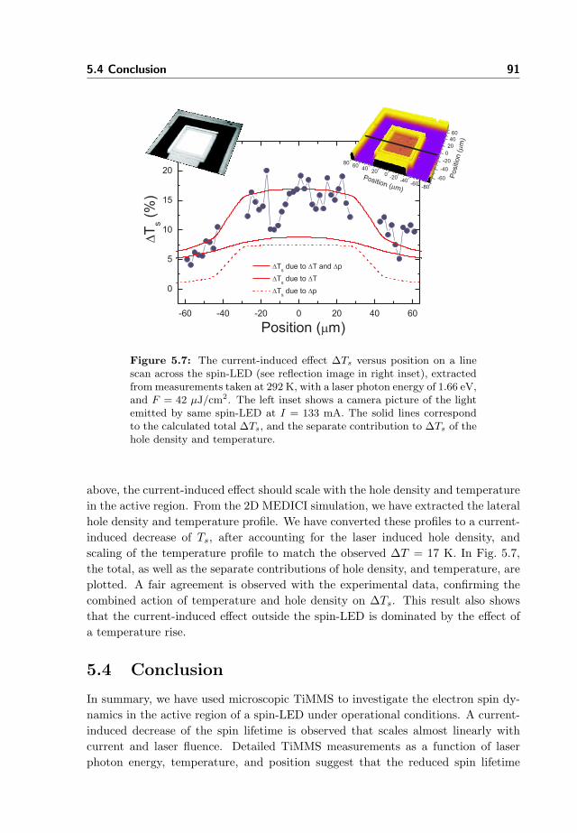
5.4 Conclusion 91
-60 -40 -20 0 20 40 60
0
5
10
15
20
25
DTs
due to DT and Dp
DTs
due to DT
DTs
due to Dp
DT
s(%
)
Position (mm)
-60
-40
-20
0
20
4060
-80-60
-40-20
020
4060
80
Position (mm)
Positio
n(m
m)
Figure 5.7: The current-induced effect ∆Ts versus position on a linescan across the spin-LED (see reflection image in right inset), extractedfrom measurements taken at 292 K, with a laser photon energy of 1.66 eV,and F = 42 µJ/cm2. The left inset shows a camera picture of the lightemitted by same spin-LED at I = 133 mA. The solid lines correspondto the calculated total ∆Ts, and the separate contribution to ∆Ts of thehole density and temperature.
above, the current-induced effect should scale with the hole density and temperaturein the active region. From the 2D MEDICI simulation, we have extracted the lateralhole density and temperature profile. We have converted these profiles to a current-induced decrease of Ts, after accounting for the laser induced hole density, andscaling of the temperature profile to match the observed ∆T = 17 K. In Fig. 5.7,the total, as well as the separate contributions of hole density, and temperature, areplotted. A fair agreement is observed with the experimental data, confirming thecombined action of temperature and hole density on ∆Ts. This result also showsthat the current-induced effect outside the spin-LED is dominated by the effect ofa temperature rise.
5.4 Conclusion
In summary, we have used microscopic TiMMS to investigate the electron spin dy-namics in the active region of a spin-LED under operational conditions. A current-induced decrease of the spin lifetime is observed that scales almost linearly withcurrent and laser fluence. Detailed TiMMS measurements as a function of laserphoton energy, temperature, and position suggest that the reduced spin lifetime
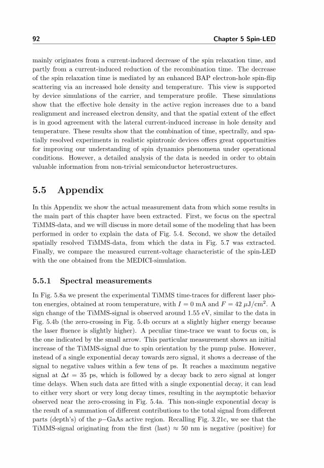
92 Chapter 5 Spin-LED
mainly originates from a current-induced decrease of the spin relaxation time, andpartly from a current-induced reduction of the recombination time. The decreaseof the spin relaxation time is mediated by an enhanced BAP electron-hole spin-flipscattering via an increased hole density and temperature. This view is supportedby device simulations of the carrier, and temperature profile. These simulationsshow that the effective hole density in the active region increases due to a bandrealignment and increased electron density, and that the spatial extent of the effectis in good agreement with the lateral current-induced increase in hole density andtemperature. These results show that the combination of time, spectrally, and spa-tially resolved experiments in realistic spintronic devices offers great opportunitiesfor improving our understanding of spin dynamics phenomena under operationalconditions. However, a detailed analysis of the data is needed in order to obtainvaluable information from non-trivial semiconductor heterostructures.
5.5 Appendix
In this Appendix we show the actual measurement data from which some results inthe main part of this chapter have been extracted. First, we focus on the spectralTiMMS-data, and we will discuss in more detail some of the modeling that has beenperformed in order to explain the data of Fig. 5.4. Second, we show the detailedspatially resolved TiMMS-data, from which the data in Fig. 5.7 was extracted.Finally, we compare the measured current-voltage characteristic of the spin-LEDwith the one obtained from the MEDICI-simulation.
5.5.1 Spectral measurements
In Fig. 5.8a we present the experimental TiMMS time-traces for different laser pho-ton energies, obtained at room temperature, with I = 0 mA and F = 42 µJ/cm2. Asign change of the TiMMS-signal is observed around 1.55 eV, similar to the data inFig. 5.4b (the zero-crossing in Fig. 5.4b occurs at a slightly higher energy becausethe laser fluence is slightly higher). A peculiar time-trace we want to focus on, isthe one indicated by the small arrow. This particular measurement shows an initialincrease of the TiMMS-signal due to spin orientation by the pump pulse. However,instead of a single exponential decay towards zero signal, it shows a decrease of thesignal to negative values within a few tens of ps. It reaches a maximum negativesignal at ∆t = 35 ps, which is followed by a decay back to zero signal at longertime delays. When such data are fitted with a single exponential decay, it can leadto either very short or very long decay times, resulting in the asymptotic behaviorobserved near the zero-crossing in Fig. 5.4a. This non-single exponential decay isthe result of a summation of different contributions to the total signal from differentparts (depth’s) of the p−GaAs active region. Recalling Fig. 3.21c, we see that theTiMMS-signal originating from the first (last) ≈ 50 nm is negative (positive) for
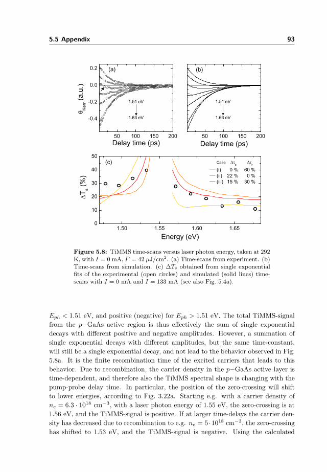
5.5 Appendix 93
1.50 1.55 1.60 1.650
10
20
30
40
50 Case
s
r
(i) 0 % 60 % (ii) 22 % 0 % (iii) 15 % 30 %
T s (%)
Energy (eV)
50 100 150 200
-0.4
-0.2
0.0
0.2
(c)
(b)
Ker
r (a.u
.)
Delay time (ps)
1.51 eV
1.63 eV
(a)
1.51 eV
1.63 eV
50 100 150 200
Delay time (ps)
Figure 5.8: TiMMS time-scans versus laser photon energy, taken at 292K, with I = 0 mA, F = 42 µJ/cm2. (a) Time-scans from experiment. (b)Time-scans from simulation. (c) ∆Ts obtained from single exponentialfits of the experimental (open circles) and simulated (solid lines) time-scans with I = 0 mA and I = 133 mA (see also Fig. 5.4a).
Eph < 1.51 eV, and positive (negative) for Eph > 1.51 eV. The total TiMMS-signalfrom the p−GaAs active region is thus effectively the sum of single exponentialdecays with different positive and negative amplitudes. However, a summation ofsingle exponential decays with different amplitudes, but the same time-constant,will still be a single exponential decay, and not lead to the behavior observed in Fig.5.8a. It is the finite recombination time of the excited carriers that leads to thisbehavior. Due to recombination, the carrier density in the p−GaAs active layer istime-dependent, and therefore also the TiMMS spectral shape is changing with thepump-probe delay time. In particular, the position of the zero-crossing will shiftto lower energies, according to Fig. 3.22a. Starting e.g. with a carrier density ofne = 6.3 · 1018 cm−3, with a laser photon energy of 1.55 eV, the zero-crossing is at1.56 eV, and the TiMMS-signal is positive. If at larger time-delays the carrier den-sity has decreased due to recombination to e.g. ne = 5 ·1018 cm−3, the zero-crossinghas shifted to 1.53 eV, and the TiMMS-signal is negative. Using the calculated
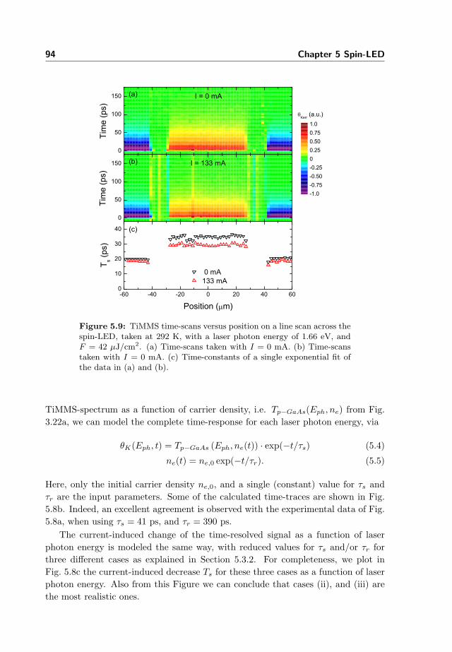
94 Chapter 5 Spin-LED
-60 -40 -20 0 20 40 600
10
20
30
40
0
50
100
150
Tim
e (p
s)
-1.0-0.75-0.50-0.2500.250.500.751.0
Kerr (a.u.)
0
50
100
150
(c)
(b) I = 133 mA
Tim
e (p
s)I = 0 mA(a)
0 mA133 mA
T s (ps
)
Position ( m)
Figure 5.9: TiMMS time-scans versus position on a line scan across thespin-LED, taken at 292 K, with a laser photon energy of 1.66 eV, andF = 42 µJ/cm2. (a) Time-scans taken with I = 0 mA. (b) Time-scanstaken with I = 0 mA. (c) Time-constants of a single exponential fit ofthe data in (a) and (b).
TiMMS-spectrum as a function of carrier density, i.e. Tp−GaAs(Eph, ne) from Fig.3.22a, we can model the complete time-response for each laser photon energy, via
θK(Eph, t) = Tp−GaAs (Eph, ne(t)) · exp(−t/τs) (5.4)
ne(t) = ne,0 exp(−t/τr). (5.5)
Here, only the initial carrier density ne,0, and a single (constant) value for τs andτr are the input parameters. Some of the calculated time-traces are shown in Fig.5.8b. Indeed, an excellent agreement is observed with the experimental data of Fig.5.8a, when using τs = 41 ps, and τr = 390 ps.
The current-induced change of the time-resolved signal as a function of laserphoton energy is modeled the same way, with reduced values for τs and/or τr forthree different cases as explained in Section 5.3.2. For completeness, we plot inFig. 5.8c the current-induced decrease Ts for these three cases as a function of laserphoton energy. Also from this Figure we can conclude that cases (ii), and (iii) arethe most realistic ones.
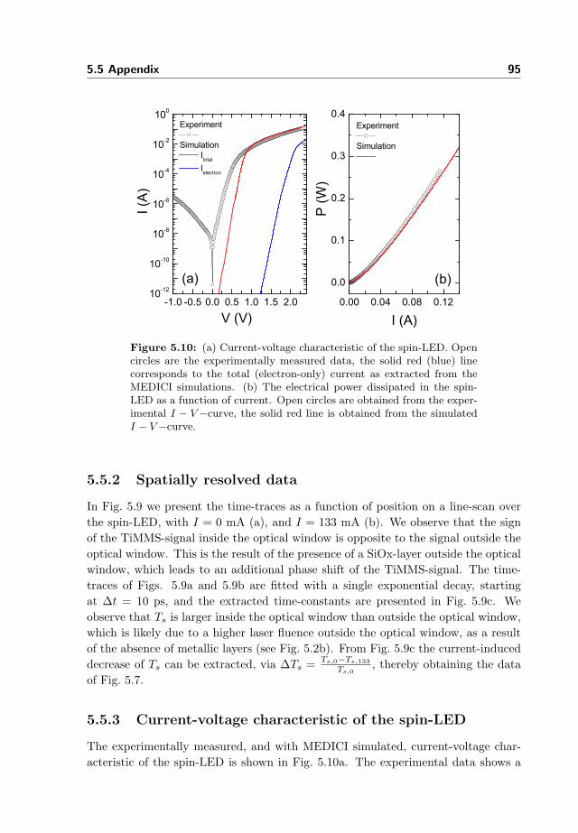
5.5 Appendix 95
-1.0 -0.5 0.0 0.5 1.0 1.5 2.010-12
10-10
10-8
10-6
10-4
10-2
100
0.00 0.04 0.08 0.12
0.0
0.1
0.2
0.3
0.4Experiment
Simulation Itotal
Ielectron
I (A
)
V (V)
(b)
Experiment
Simulation
P (W
)I (A)
(a)
Figure 5.10: (a) Current-voltage characteristic of the spin-LED. Opencircles are the experimentally measured data, the solid red (blue) linecorresponds to the total (electron-only) current as extracted from theMEDICI simulations. (b) The electrical power dissipated in the spin-LED as a function of current. Open circles are obtained from the exper-imental I − V−curve, the solid red line is obtained from the simulatedI − V−curve.
5.5.2 Spatially resolved data
In Fig. 5.9 we present the time-traces as a function of position on a line-scan overthe spin-LED, with I = 0 mA (a), and I = 133 mA (b). We observe that the signof the TiMMS-signal inside the optical window is opposite to the signal outside theoptical window. This is the result of the presence of a SiOx-layer outside the opticalwindow, which leads to an additional phase shift of the TiMMS-signal. The time-traces of Figs. 5.9a and 5.9b are fitted with a single exponential decay, startingat ∆t = 10 ps, and the extracted time-constants are presented in Fig. 5.9c. Weobserve that Ts is larger inside the optical window than outside the optical window,which is likely due to a higher laser fluence outside the optical window, as a resultof the absence of metallic layers (see Fig. 5.2b). From Fig. 5.9c the current-induceddecrease of Ts can be extracted, via ∆Ts = Ts,0−Ts,133
Ts,0, thereby obtaining the data
of Fig. 5.7.
5.5.3 Current-voltage characteristic of the spin-LED
The experimentally measured, and with MEDICI simulated, current-voltage char-acteristic of the spin-LED is shown in Fig. 5.10a. The experimental data shows a
96 Chapter 5 Spin-LED
non-linear I−V−curve, characteristic for these spin-LEDs [15]. The I−V−curve ob-tained from the MEDICI simulation shows an almost quantitative agreement withthe experimental curve for an applied bias larger than 1 V, which is the regimeabove luminescence threshold. This indicates that the MEDICI simulation is rep-resentative for the actual device. Below 1 V, the simulated current is lower thanexperimentally observed. The probable origin for this discrepancy is the fact thatMEDICI does not take into account the filling of surface states at the AlGaAsinterface by electrons tunneling from the electrode.
Figure 5.5.3b shows the dissipated power, P , in the spin-LED as a function ofcurrent extracted from both the experimental as well as the simulated I−V−curve.Again an good quantitative agreement between the experimental and simulatedcurve is observed. We note that for I > 0.05 mA, the dependence of P on I can bewell described by a linear relationship.
BIBLIOGRAPHY 97
Bibliography
[1] I. Zutic, J. Fabian, S. Das Sarma, Spintronics: Fundamentals and applications,Rev. Mod. Phys. 76, 323-410 (2004). 5.1
[2] G. L. Bir, A. G. Aronov, and G. E. Pikus, Spin relaxation of electrons due toscattering by holes, Zh. Eksp. Teor. Fiz. 69, 1382-1397 (1975) [Sov. Phys. JETP42, 705-712 (1976)]. 5.1
[3] A. G. Aronov, G. E. Pikus, and A. N. Titkov, Spin relaxation of conductionelectrons in p-type III-V compounds, Zh. Eksp. Teor. Fiz. 84, 1170-1184 (1983)[Sov. Phys. JETP 57, 680-687 (1983)]. 5.3.1, 5.5, 5.3.2
[4] K. Zerrouati, F. Fabre, G. Bacquet, J. B. J. Frandon, G. Lampel, and D. Paget,Spin-lattice relaxation in p-type gallium arsenide single crystals, Phys. Rev. B37, 1334-1341 (1988).
[5] J. M. Kikkawa, and D. D. Awschalom, Resonant spin amplification in n-typeGaAs, Phys. Rev. Lett. 80, 4313-4316 (1998).
[6] Y. Ohno, Y., R. Terauchi, F. Matsukura, and H. Ohno, Spin relaxation inGaAs(110) quantum wells, Phys. Rev. Lett. 83, 4196-4199 (1999).
[7] A. Malinowski, R. S. Britton, T. Grevatt, R. T. Harley, D. A. Ritschie, and M.Y. Simmons, Spin relaxation in GaAs/AlxGa1−xAs quantum wells, Phys. Rev.B 62, 13034-13039 (2000).
[8] P. H. Song, and K. W. Kim, Spin relaxation of conduction electrons in bulkIII-V semiconductors, Phys. Rev. B 66, 035207 (2002). 5.1
[9] B. Koopmans, J. E. M. Haverkort, W. J. M. de Jonge, and G. Karczewski,Time-resolved magnetization modulation spectroscopy: A new probe of ultrafastspin dynamics, J. Appl. Phys. 85, 6763 (1999). 5.2.1
[10] B. Koopmans, and W. J. M. de Jonge, Ultrafast spin dynamics in mag-netic semiconductor quantum wells studied by magnetization modulation spec-troscopy, Appl. Phys. B 68, 525 (1999). 5.2.1, 5.3.2
[11] R. Fiederling, M. Kleim, G. Reuscher, W. Ossau, G. Schmidt, A. Waag, and L.W. Molenkamp, Injection and detection of a spin-polarized current in a light-emitting diode, Nature (London) 402, 787-790 (1999). 5.2.1
[12] A. T. Hanbicki, B. T. Jonker, G. Itskos, G. Kioseoglou, and A. Petrou, Efficientelectrical spin injection from a magnetic metal/tunnel barrier contact into asemiconductor, Appl. Phys. Lett. 80, 1240-1242 (2002).
98 Chapter 5 Spin-LED
[13] V. F. Motsnyi, V. I. Safarov, J. De Boeck, J. Das, W. Van Roy, E.Goovaerts, and G. Borghs, Electrical spin injection in a ferromagnet/tunnelbarrier/semiconductor heterostructure, Appl. Phys. Lett. 81, 265-267 (2002).5.2.1, 5.2.2
[14] C. A. C. Bosco, D. Snouck, P. Van Dorpe, W. Van Roy, and B. Koopmans,Bias-dependent spin relaxation in a spin-LED, Mater. Sci. Eng. B 126, 107(2006). 5.2.2
[15] V. F. Motsnyi, P. Van Dorpe, W. Van Roy, E. Goovaerts, V. I. Safarov, G.Borghs, and J. De Boeck, Optical investigation of electrical spin injection intosemiconductors, Phys. Rev. B 68, 245319 (2003). 5.2.2, 5.5.3
[16] M. R. Brozel, and G. E. Stillman, Properties of Gallium Arsenide (3rd Edition),(London: INSPEC, 1996). 5.2.2, 5.3.2
[17] S. Adachi, Properties of Aluminium Gallium Arsenide, (London: IEE, 1993).5.2.2, 5.3.2
[18] For details, see http://www.synopsys.com. 5.3.1
[19] J. Zak, E. R. Moog, C. Liu, and S. D. Bader, Universal approach to magneto-optics, J. Magn. Magn. Mater. 89, 107-123 (1990). 5.3.2
[20] W. Van Roy, private communication. 5.3.2
[21] Y. P. Varshni, Temperature dependence of the energy gap in semiconductors,Physica 34, 149-154 (1967). 5.3.2
Chapter 6
Probing carrier and spindynamics in GaAs-basednanowires
We have studied the carrier and spin dynamics in multi-segmented GaP / GaAs
nanowires, and in single GaP-capped GaP / GaAs / GaP nanowires using an all-
optical technique. We have identified two different carrier relaxation processes,
carrier thermalization and recombination. The recombination time (≈ 10 ps) is
short compared to bulk GaAs, and independent of temperature, for both the multi-
segmented as well as the GaP-capped nanowires. This indicates a dominant non-
radiative recombination channel via surface and defect states. We show that our
two-color magneto-optical technique is capable of measuring spin dynamics within a
single nanowire. These measurements suggests that for these GaP-capped nanowires
the spin lifetime is recombination limited. This approach enables the study of carrier
and spin dynamics in single nanowires, and is complementary to (time-resolved)
photoluminescence.1
1A large part of this Chapter is in preparation for publication as J. H. H. Rietjens, C. A.C. Bosco, M. T. Borgstrom, E. P. A. M. Bakkers, and B. Koopmans, Probing carrier and spindynamics in GaAs-based nanowires
99
100 Chapter 6 Nanowires
6.1 Introduction
During the last decade the growth and use of semiconductor nanowires (NWs) hasseen a tremendous development [1, 2]. Nowadays it is possible to grow NWs exhibit-ing a wide range of diameters, lengths, and types of semiconductors, with the possi-bility to combine segments of different materials in a single wire, including varyingthe doping profile [3–5]. It has been demonstrated that NWs can be used as light-emitting diodes [3], photo-detectors [6], field-effect transistors [7], and bio/chemicalsensors [8, 9]. Moreover, NWs provide the possibility to integrate the superioroptical and electrical properties of III/V semiconductors with the well-establishedSi-technology [10, 11]. Yet another promising application of semiconductor NWscould be their use as potential building blocks for spintronic devices, exploiting thespin degree of freedom. The one-dimensional nature and quantum confinement ef-fects of NWs can be used to make e.g. spin-based transistors or spin-based qubits forquantum computation. For this purpose the electron spin decoherence time shouldbe long enough to perform spin operations. It is therefore important to study andcontrol the carrier and spin dynamics in individual NWs.
In this Chapter we report on the characterization of the carrier relaxation time,and electron spin dephasing time in GaAs-based NWs with a microscopic time- andspatially-resolved all-optical approach. We have chosen for the GaP/GaAs system,as GaAs is one of the main high performance III/V systems, and can have highradiative lifetimes and high spin dephasing times in bulk and quantum well sys-tems under certain temperature and doping conditions. We have studied ensemblesof multi-segmented GaP/GaAs NWs, and performed single wire experiments onGaP-capped GaP/GaAs/GaP-NWs. We will discuss the observed carrier relaxationprocesses in connection with the observed spin lifetime, and demonstrate that usingthis technique it is possible to address carrier and spin dynamics in single nanowires.
6.2 Experimental details
A microscopic all-optical time-resolved pump-probe technique is used in order todirectly measure the carrier and spin dynamics in the NW after excitation. A mode-locked Ti:Sapphire laser produces laser pulses (≈ 100 fs temporal width, 80 MHzrepetition rate) with photon energies ranging from 1.45 to 1.67 eV. The laser pulsesare divided in strong pump and weak probe pulses. Pump and probe beam are fo-cused to an overlapping spot on the sample in an optical cryostat. In the transient re-flectivity (TR) configuration, the pump beam is linearly polarized (p−polarization)and excites (non spin-polarized) electron-hole pairs in the NW, thereby changing theoptical reflection and absorption constants. The time-dependent change in opticalconstant is measured via the TR of the s−polarized probe beam. In this way thesetup is sensitive to the carrier dynamics, such as carrier thermalization and carrierrecombination, but also detects other pump related changes to the dielectric tensor
6.3 Probing ensembles of multi-segmented GaP / GaAs nanowires 101
such as heating. In the Magneto-Optical (MO) configuration, the pump beam iscircularly polarized in order to excite electron spins via the optical selection rules ofzinc-blende semiconductors. The excited spins are probed via the magneto-opticalKerr-effect (MOKE) experienced by the linearly polarized probe beam after reflec-tion from the sample. In this configuration the MO-signal depends on the spinlifetime Ts, which is related to the spin relaxation time τs, and the carrier recombi-nation time τr via T−1
s = τ−1s + τ−1
r . Time resolution is obtained by delaying theprobe beam with respect to the pump beam with a mechanical translation stage.In order to study the ensemble wires, we used an objective resulting in a spot sizeof ≈ 20 µm for pump and probe. For single wire measurements we used a differentobjective, resulting in a spot size of ≈ 3 µm of the probe (and ≈ 7 µm pump spotsize). Time-resolved measurements were performed at a temperature of 5 K androom temperature (RT).
6.3 Probing ensembles of multi-segmented GaP /GaAs nanowires
Let us first consider our measurements on an ensemble of multi-segmented GaP/ GaAs NWs. Samples for the NW growth were prepared by dispersing 20 nmdiameter Au colloids on a thermally oxidized (500 nm) Si substrate. The NWswere grown via the Vapor-Liquid-Solid growth technique by using Metallo-Organic-Vapor-Phase-Epitaxy (MOVPE) with trimethylgallium (TMG), phosphine (PH3),and arsine (AsH3) as precursors in a H2 environment. The first segment of thewire is a GaP-segment, which is followed by alternating GaAs and GaP segmentsby switching the group V precursors in the growth chamber. Details of the growthtechnique have been described in reports on the growth kinetics [12], and interfacechemical composition [5] of such wires. The diameter of the NWs is ≈ 20 nm, andthe length of the smallest segment is ≈ 25 nm, so no quantum confinement effectsare expected. A high-angle annular dark-field transmission microscope (HAADF-TEM) image of the resulting NW is shown in the inset of Fig. 6.1. The individualGaP and GaAs segments and the Au catalyst particle are clearly visible. The NWare oriented in random directions and we estimate the density to be ≈ 108 cm−2.A microscope picture of a part of the NW sample is also shown in the inset of Fig.6.1.
6.3.1 Transient reflectivity measurements
We performed time resolved transient reflectivity (TR) measurements on these wiresin order to study the carrier dynamics. With a ≈ 20 µm spot size, we estimate thatwe average over an ensemble of 102 to 103 wires. A typical TR measurement takenat a temperature of 5 K with a laser photon energy of 1.59 eV is shown in Fig. 6.1.After a fast decrease of the transient reflectivity at ∆t = 0, the signal recovers to
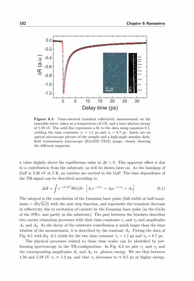
102 Chapter 6 Nanowires
0 5 10 15 20 25 30
-1.2
-1.0
-0.8
-0.6
-0.4
-0.2
0.0D
R(a
.u.)
Delay time (ps)
GaP
GaP
GaP
GaP
GaP
GaAs
GaAs
GaAs
GaAs
GaAs
Figure 6.1: Time-resolved transient reflectivity measurement on theensemble wires, taken at a temperature of 5 K, and a laser photon energyof 1.59 eV. The solid line represents a fit to the data using equation 6.1,yielding the time constants τ1 = 1.1 ps and τ2 = 8.7 ps. Insets are anoptical microscope picture of the sample and a high-angle annular dark-field transmission microscope (HAADF-TEM) image, clearly showingthe different segments.
a value slightly above the equilibrium value at ∆t < 0. This apparent offset is dueto a contribution from the substrate, as will be shown later on. As the bandgap ofGaP is 2.26 eV at 5 K, no carriers are excited in the GaP. The time dependence ofthe TR-signal can be described according to
∆R =∫
e−(t/d)2Θ(t)dt ·[A1e
−t/τ1 + A2e−t/τ2 + A3
](6.1)
The integral is the convolution of the Gaussian laser pulse (full-width at half maxi-mum = d2
√ln 2) with the unit step function, and represents the transient decrease
in reflectivity due to excitation of carriers by the Gaussian laser pulse (in the GaAsof the NWs, and partly in the substrate). The part between the brackets describestwo carrier relaxation processes with their time constants τ1 and τ2 and amplitudesA1 and A2. As the decay of the substrate contribution is much larger than the timewindow of the measurement, it is described by the constant A3. Fitting the data ofFig. 6.1 with Eq. 6.1 yields for the two time constant τ1 = 1.1 ps and τ2 = 8.7 ps.
The physical processes related to these time scales can be identified by per-forming spectroscopy in the TR-configuration. In Fig. 6.2 we plot τ1 and τ2 andthe corresponding amplitudes A1 and A2 vs. photon energy. We see that between1.50 and 1.59 eV τ1 ≈ 1.2 ps, and that τ1 decreases to ≈ 0.5 ps at higher energy.
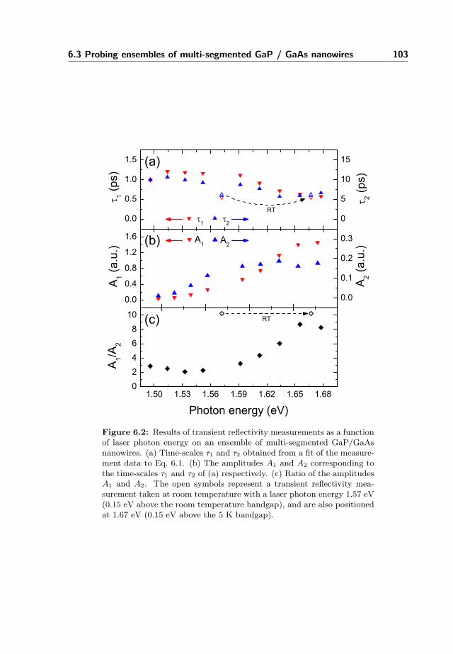
6.3 Probing ensembles of multi-segmented GaP / GaAs nanowires 103
0.0
0.5
1.0
1.5
0
5
10
15
0.0
0.1
0.2
0.3
(c)
(b)
(a)
1
2 (ps)
1 (ps)
2
0.0
0.4
0.8
1.2
1.6 A1
A1 (a
.u.)
1.50 1.53 1.56 1.59 1.62 1.65 1.680
24
68
10 RT
A1/A
2
Photon energy (eV)
RT
A2
A2 (a
.u.)
Figure 6.2: Results of transient reflectivity measurements as a functionof laser photon energy on an ensemble of multi-segmented GaP/GaAsnanowires. (a) Time-scales τ1 and τ2 obtained from a fit of the measure-ment data to Eq. 6.1. (b) The amplitudes A1 and A2 corresponding tothe time-scales τ1 and τ2 of (a) respectively. (c) Ratio of the amplitudesA1 and A2. The open symbols represent a transient reflectivity mea-surement taken at room temperature with a laser photon energy 1.57 eV(0.15 eV above the room temperature bandgap), and are also positionedat 1.67 eV (0.15 eV above the 5 K bandgap).
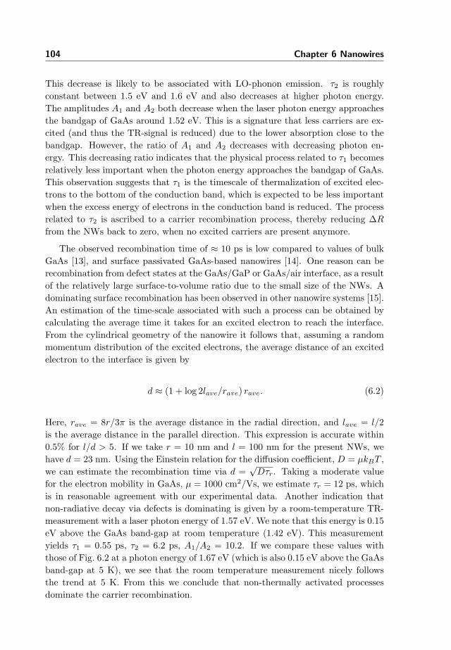
104 Chapter 6 Nanowires
This decrease is likely to be associated with LO-phonon emission. τ2 is roughlyconstant between 1.5 eV and 1.6 eV and also decreases at higher photon energy.The amplitudes A1 and A2 both decrease when the laser photon energy approachesthe bandgap of GaAs around 1.52 eV. This is a signature that less carriers are ex-cited (and thus the TR-signal is reduced) due to the lower absorption close to thebandgap. However, the ratio of A1 and A2 decreases with decreasing photon en-ergy. This decreasing ratio indicates that the physical process related to τ1 becomesrelatively less important when the photon energy approaches the bandgap of GaAs.This observation suggests that τ1 is the timescale of thermalization of excited elec-trons to the bottom of the conduction band, which is expected to be less importantwhen the excess energy of electrons in the conduction band is reduced. The processrelated to τ2 is ascribed to a carrier recombination process, thereby reducing ∆R
from the NWs back to zero, when no excited carriers are present anymore.
The observed recombination time of ≈ 10 ps is low compared to values of bulkGaAs [13], and surface passivated GaAs-based nanowires [14]. One reason can berecombination from defect states at the GaAs/GaP or GaAs/air interface, as a resultof the relatively large surface-to-volume ratio due to the small size of the NWs. Adominating surface recombination has been observed in other nanowire systems [15].An estimation of the time-scale associated with such a process can be obtained bycalculating the average time it takes for an excited electron to reach the interface.From the cylindrical geometry of the nanowire it follows that, assuming a randommomentum distribution of the excited electrons, the average distance of an excitedelectron to the interface is given by
d ≈ (1 + log 2lave/rave) rave. (6.2)
Here, rave = 8r/3π is the average distance in the radial direction, and lave = l/2is the average distance in the parallel direction. This expression is accurate within0.5% for l/d > 5. If we take r = 10 nm and l = 100 nm for the present NWs, wehave d = 23 nm. Using the Einstein relation for the diffusion coefficient, D = µkBT ,we can estimate the recombination time via d =
√Dτr. Taking a moderate value
for the electron mobility in GaAs, µ = 1000 cm2/Vs, we estimate τr = 12 ps, whichis in reasonable agreement with our experimental data. Another indication thatnon-radiative decay via defects is dominating is given by a room-temperature TR-measurement with a laser photon energy of 1.57 eV. We note that this energy is 0.15eV above the GaAs band-gap at room temperature (1.42 eV). This measurementyields τ1 = 0.55 ps, τ2 = 6.2 ps, A1/A2 = 10.2. If we compare these values withthose of Fig. 6.2 at a photon energy of 1.67 eV (which is also 0.15 eV above the GaAsband-gap at 5 K), we see that the room temperature measurement nicely followsthe trend at 5 K. From this we conclude that non-thermally activated processesdominate the carrier recombination.
6.3 Probing ensembles of multi-segmented GaP / GaAs nanowires 105
0 10 20 30 40
-0.4
-0.3
-0.2
-0.1
0.0
s = 6.0 ± 0.3
Ker
r (a.u
.)
Delay time (ps)
Figure 6.3: Time-resolved magneto-optical measurement on the en-semble wires, taken at a temperature of 5 K, and a laser photon energyof 1.57 eV. The solid line represents a single exponential fit to the data,yielding a time constant of 6.0 ps.
6.3.2 Magneto-optical measurements
The short recombination time determined above implies that the timescale of thespin signal we might detect in a MO experiment is at most of the order of 10 ps,even when the spin relaxation time is much higher. The carrier lifetime determinesin this case the spin lifetime, and thus the decrease of the MO-signal, via T−1
s =τ−1s +τ−1
r . We performed MO measurements on the ensemble of nanowires, of whicha representative result, taken at a laser photon energy of 1.57 eV, is shown in Fig. 6.3.The signal-to-noise ratio for this measurement is a factor ≈ 103 lower than for theTR-measurement. We attribute this to the effect of a strong polarization anisotropy[6] exhibited by these NWs. Due to the polarization anisotropy, the NW effectivelyacts as a polarizer, limiting the penetration of circularly polarized light. This leadsto a strongly reduced efficiency of excitation of spins via the optical selection rules,and also to a strongly reduced detection sensitivity of electron spins via the MOKE,which decreases the efficiency of optical spin injection and detection. The sharpincrease of the MO-signal at ∆t = 0 is a signature of optical spin orientation due tothe pump pulse, and is followed by a fast decay to its equilibrium value. In order toextract the time-scale of this decay, we can again use Eq. 6.1 to fit the data. SettingA2 to zero (single exponential decay) yields for the spin lifetime τ1 = Ts = 6.0 ps.Although an effect of carrier thermalization on the MO-signal is not observed, wenote that the extracted Ts is close to the recombination time τ2, which might indicatea recombination limited spin lifetime.
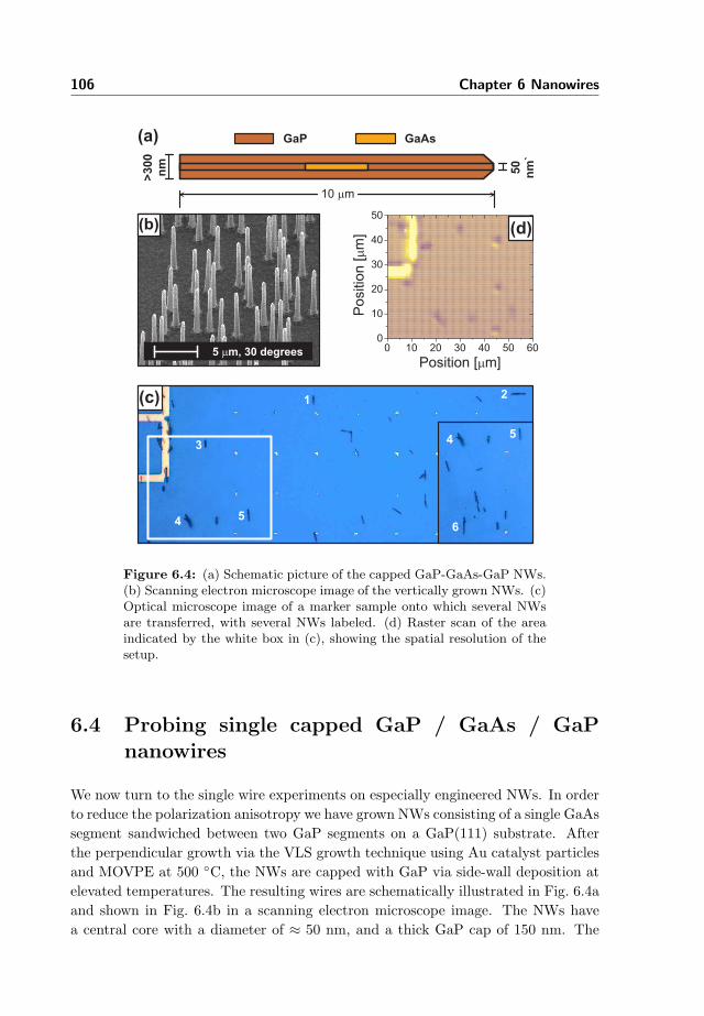
106 Chapter 6 Nanowires
0 10 20 30 40 50 600
10
20
30
40
50
Position [mm]P
ositio
n[m
m]
50
nm
`
>300
nm
GaP GaAs(a)
5 m, 30 degreesm
(b)
(c)
(d)
10 mm
3
45
12
45
6
Figure 6.4: (a) Schematic picture of the capped GaP-GaAs-GaP NWs.(b) Scanning electron microscope image of the vertically grown NWs. (c)Optical microscope image of a marker sample onto which several NWsare transferred, with several NWs labeled. (d) Raster scan of the areaindicated by the white box in (c), showing the spatial resolution of thesetup.
6.4 Probing single capped GaP / GaAs / GaPnanowires
We now turn to the single wire experiments on especially engineered NWs. In orderto reduce the polarization anisotropy we have grown NWs consisting of a single GaAssegment sandwiched between two GaP segments on a GaP(111) substrate. Afterthe perpendicular growth via the VLS growth technique using Au catalyst particlesand MOVPE at 500 ◦C, the NWs are capped with GaP via side-wall deposition atelevated temperatures. The resulting wires are schematically illustrated in Fig. 6.4aand shown in Fig. 6.4b in a scanning electron microscope image. The NWs havea central core with a diameter of ≈ 50 nm, and a thick GaP cap of 150 nm. The
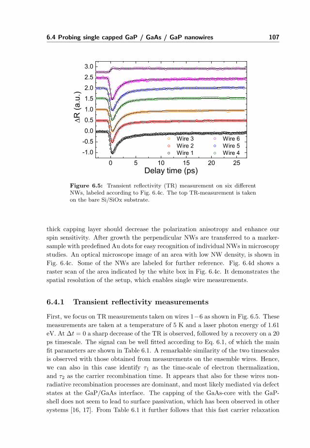
6.4 Probing single capped GaP / GaAs / GaP nanowires 107
0 5 10 15 20 25
-1.0
-0.5
0.0
0.5
1.0
1.5
2.0
2.5
3.0
Wire 3 Wire 6 Wire 2 Wire 5 Wire 1 Wire 4
R (a
.u.)
Delay time (ps)
Figure 6.5: Transient reflectivity (TR) measurement on six differentNWs, labeled according to Fig. 6.4c. The top TR-measurement is takenon the bare Si/SiOx substrate.
thick capping layer should decrease the polarization anisotropy and enhance ourspin sensitivity. After growth the perpendicular NWs are transferred to a marker-sample with predefined Au dots for easy recognition of individual NWs in microscopystudies. An optical microscope image of an area with low NW density, is shown inFig. 6.4c. Some of the NWs are labeled for further reference. Fig. 6.4d shows araster scan of the area indicated by the white box in Fig. 6.4c. It demonstrates thespatial resolution of the setup, which enables single wire measurements.
6.4.1 Transient reflectivity measurements
First, we focus on TR measurements taken on wires 1−6 as shown in Fig. 6.5. Thesemeasurements are taken at a temperature of 5 K and a laser photon energy of 1.61eV. At ∆t = 0 a sharp decrease of the TR is observed, followed by a recovery on a 20ps timescale. The signal can be well fitted according to Eq. 6.1, of which the mainfit parameters are shown in Table 6.1. A remarkable similarity of the two timescalesis observed with those obtained from measurements on the ensemble wires. Hence,we can also in this case identify τ1 as the time-scale of electron thermalization,and τ2 as the carrier recombination time. It appears that also for these wires non-radiative recombination processes are dominant, and most likely mediated via defectstates at the GaP/GaAs interface. The capping of the GaAs-core with the GaP-shell does not seem to lead to surface passivation, which has been observed in othersystems [16, 17]. From Table 6.1 it further follows that this fast carrier relaxation
108 Chapter 6 Nanowires
Table 6.1: Parameters of a fit of Eq. 6.1 to the transient reflectivitysignal of the six labeled NWs in Figure 6.5.
Wire τ1 (ps) τ2 (ps) A1 A2
1 1.3 9.2 -5.7 -1.02 1.1 10.9 -6.9 -0.83 1.4 7.2 -6.4 -0.74 1.2 5.5 -6.7 -1.25 1.2 7.5 -6.8 -1.36 1.2 12.9 -6.5 -0.6
is characteristic for all wires from which a decent TR-signal could be obtained. Thetop TR-measurement in Fig. 6.5 is taken on the bare Si/SiOx substrate, and showsa step-like signal, which we attribute to excited carriers in the Si, which have arelatively long recombination time due to the indirect bandgap of Si. We note thatthis contribution, to some extend, is present in all single wire measurements, and isalso observed in the ensemble measurement of Figs. 6.1 and 6.2.
In Fig. 6.6 we present measurements performed on different positions on a linescan over NW 5. It shows the reflection of the probe beam, the TR-signal at afixed time delay of 1 ps, and an image containing time-traces, all as a function ofposition. The three segments of the wire can be clearly identified in the reflectionscan (Fig. 6.6a), where the reflectivity of the center GaAs segment is slightly higherthan the reflectivity of the two GaP segments. In the TR-scan (Fig. 6.6b) only theGaAs segment can be recognized, indicating that only in this segment free carriersare excited. This is expected because the laser photon energy (1.6 eV) is belowthe indirect bandgap of GaP (2.26 eV), but above that of GaAs (1.52 eV). Thetime-resolved signals in color scale show that for positions < −6 µm and > 6 µm,the measurement data is similar to the top measurement of Fig. 6.2, and originatesfrom the Si substrate. Also, as expected from the TR-scan, only on the positionsthat match the GaAs segment a clear TR-signal is observed. This proves that weare indeed probing (parts of) a single nanowire.
6.4.2 Magneto-optical measurements
Let us now turn to the magneto-optical (MO) measurements taken on NWs 1 and6, which are shown in Fig 6.7. Here we see, surprisingly, an exponentially decayingsignal both in the positive as well as in the negative delay time direction. This canbe understood if we consider the fact that a single nanowire is an effective scatterer,since the width is much smaller than our laser spot. Therefore, a significant portionof the pump laser pulse is scattered in all directions, including towards the detector.This scattered pump light contains information of excited carriers when the pumpbeam arrives later at the sample than the probe beam, in a similar way as in the
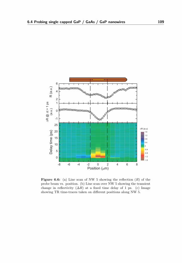
6.4 Probing single capped GaP / GaAs / GaP nanowires 109
-8 -6 -4 -2 0 2 4 6 8
0
5
10
15
20
25
Position (mm)
Dela
ytim
e(p
s) DR (a.u)
-1.6
-1.2
-0.8
-0.4
0
0.4
0.8
1.2
1.6
-1
0
1
DR
@D
t=
1p
s
(a.u
.)
2
4
6
R(a
.u.)
Figure 6.6: (a) Line scan of NW 5 showing the reflection (R) of theprobe beam vs. position. (b) Line scan over NW 5 showing the transientchange in reflectivity (∆R) at a fixed time delay of 1 ps. (c) Imageshowing TR time-traces taken on different positions along NW 5.
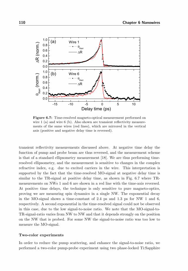
110 Chapter 6 Nanowires
-15 -10 -5 0 5 10
0.00.20.40.60.81.0
Ker
r (nor
m.)
Delay time (ps)
0.00.20.40.60.81.0
R (n
orm
.)
(b) Wire 6 Kerr
R
Wire 1 Kerr
R
(a)
Figure 6.7: Time-resolved magneto-optical measurement performed onwire 1 (a) and wire 6 (b). Also shown are transient reflectivity measure-ments of the same wires (red lines), which are mirrored in the verticalaxis (positive and negative delay time is reversed).
transient reflectivity measurements discussed above. At negative time delay thefunction of pump and probe beam are thus reversed, and the measurement schemeis that of a standard ellipsometry measurement [18]. We are thus performing time-resolved ellipsometry, and the measurement is sensitive to changes in the complexrefractive index, e.g. due to excited carriers in the wire. This interpretation issupported by the fact that the time-resolved MO-signal at negative delay time issimilar to the TR-signal at positive delay time, as shown in Fig. 6.7 where TR-measurements on NWs 1 and 6 are shown in a red line with the time-axis reversed.At positive time delays, the technique is only sensitive to pure magneto-optics,proving we are measuring spin dynamics in a single NW. The exponential decayin the MO-signal shows a time-constant of 2.4 ps and 1.3 ps for NW 1 and 6,respectively. A second exponential in the time-resolved signal could not be observedin this case, due to the low signal-to-noise ratio. We note that the MO-signal-to-TR-signal-ratio varies from NW to NW and that it depends strongly on the positionon the NW that is probed. For some NW the signal-to-noise ratio was too low tomeasure the MO-signal.
Two-color experiments
In order to reduce the pump scattering, and enhance the signal-to-noise ratio, weperformed a two-color pump-probe experiment using two phase-locked Ti:Sapphire
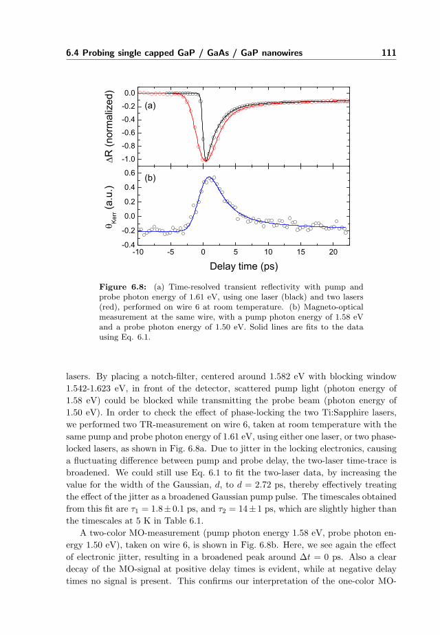
6.4 Probing single capped GaP / GaAs / GaP nanowires 111
-1.0
-0.8
-0.6
-0.4
-0.2
0.0
(b)
R (n
orm
aliz
ed)
(a)
-10 -5 0 5 10 15 20-0.4
-0.2
0.0
0.2
0.4
0.6
Ker
r (a.u
.)
Delay time (ps)
Figure 6.8: (a) Time-resolved transient reflectivity with pump andprobe photon energy of 1.61 eV, using one laser (black) and two lasers(red), performed on wire 6 at room temperature. (b) Magneto-opticalmeasurement at the same wire, with a pump photon energy of 1.58 eVand a probe photon energy of 1.50 eV. Solid lines are fits to the datausing Eq. 6.1.
lasers. By placing a notch-filter, centered around 1.582 eV with blocking window1.542-1.623 eV, in front of the detector, scattered pump light (photon energy of1.58 eV) could be blocked while transmitting the probe beam (photon energy of1.50 eV). In order to check the effect of phase-locking the two Ti:Sapphire lasers,we performed two TR-measurement on wire 6, taken at room temperature with thesame pump and probe photon energy of 1.61 eV, using either one laser, or two phase-locked lasers, as shown in Fig. 6.8a. Due to jitter in the locking electronics, causinga fluctuating difference between pump and probe delay, the two-laser time-trace isbroadened. We could still use Eq. 6.1 to fit the two-laser data, by increasing thevalue for the width of the Gaussian, d, to d = 2.72 ps, thereby effectively treatingthe effect of the jitter as a broadened Gaussian pump pulse. The timescales obtainedfrom this fit are τ1 = 1.8±0.1 ps, and τ2 = 14±1 ps, which are slightly higher thanthe timescales at 5 K in Table 6.1.
A two-color MO-measurement (pump photon energy 1.58 eV, probe photon en-ergy 1.50 eV), taken on wire 6, is shown in Fig. 6.8b. Here, we see again the effectof electronic jitter, resulting in a broadened peak around ∆t = 0 ps. Also a cleardecay of the MO-signal at positive delay times is evident, while at negative delaytimes no signal is present. This confirms our interpretation of the one-color MO-
112 Chapter 6 Nanowires
measurement, that the signal at negative delay times is due to pump scattering. Wecan fit the full time-resolved MO-signal with Eq. 6.1, by fixing the value of d and set-ting A3 to zero, as no magneto-optical contribution from the substrate is expected.This way, we find for the two time constants τ1 = 2.6± 0.5 ps, and τ2 = 20± 16 ps.As there is a reasonable agreement with the timescales of the TR-measurement, theMO-measurement points towards a recombination limited spin lifetime.
6.5 Conclusion
Summarizing, we have performed time-resolved all-optical experiments on segmentedGaP / GaAs nanowires, thereby addressing both carrier as well as spin dynamicsin ensemble and single nanowires. The carrier recombination is observed to rangebetween 5 and 15 ps for all addressed single nanowires, which is in the range asthose obtained from the ensemble wires. This, and the fact that the carrier recom-bination time is independent of temperature, indicates a strong contribution of non-radiative recombination via defect states at the GaAs/air and GaAs/GaP interface.By performing two-color experiments on single nanowires, we have demonstratedthat our technique is capable of measuring spin dynamics within a single nanowire.These measurements suggests that for these nanowires the spin lifetime is recombi-nation limited. This approach enables studying carrier and spin dynamics in singlenanowires and is complementary to (time-resolved) photoluminescence.
BIBLIOGRAPHY 113
Bibliography
[1] C. M. Lieber, Nanoscale Science and Technology: Building a Big Future fromSmall Things, MRS Bull. 28, 486 (2003). 6.1
[2] M. Law, J. Goldberger, and P. Yang, Semiconductor nanowires and nanotubes,Annu. Rev. Mater. Res. 34, 83 (2004). 6.1
[3] X. Duan, Y. Huang, Y. Cui, J. Wang. and C. M. Lieber, Indium phosphidenanowires asbuilding blocks for nanoscaleelectronic and optoelectronic devices,Nature (London) 409, 66-69 (2001). 6.1
[4] M. S. Gudiksen, L. J. Lauhon, J. Wang, D. C. Smith, and C. M. Lieber, Growthof nanowire superlattice structures for nanoscale photonics and electronics, Na-ture (London) 415, 617 (2002).
[5] M. T. Borgstrom, M. A. Verheijen, G. Immink, T. de Smet, and E. P. A. M.Bakkers, Interface study on heterostructured GaP-GaAs nanowires, Nanotech-nology 17, 4010-4013 (2006). 6.1, 6.3
[6] J. Wang, M. S. Gudiksen, X. Duan, Y. Cui, and C. M. Lieber, Highly Po-larized Photoluminescence and Photodetection from Single Indium PhosphideNanowires, Science 293 1455 (2001). 6.1, 6.3.2
[7] J. Xiang, W. Lu, Y. Hu, Y. Wu, H. Yan, and C. M. Lieber, Ge/Si nanowireheterostructures as high-performance field-effect transistors, Nature (London)441, 04796 (2006). 6.1
[8] E. Stern, J. F. Klemic, D. A. Routenberg, P. N. Wyrembak, D. B. Turner-Evans, A. D. Hamilton, D. A. LaVan, T. M. Fahmyl, and M. A. Reed, Label-free immunodetection with CMOS-compatiblesemiconducting nanowires, Nature(London) 445, 7127 (2007). 6.1
[9] M. C. McAlpine, H. Ahmad, D. Wang, and J. R. Heath, Highly orderednanowire arrays on plasticsubstrates for ultrasensitive flexiblechemical sensors,Nat. Mater. 6, 379-384 (2007). 6.1
[10] T. Martensson, C. Patrik, T. Svensson, B. A. Wacaser, M. W. Larsson, W.Seifert, K. Deppert, A. Gustafsson, L. R. Wallenberg, and L. Samuelson, Epi-taxial III-V nanowires on silicon, Nano Lett. 4, 1987-1990 (2004). 6.1
[11] E. P. A. M. Bakkers, J. A. van Dam, S. De Franceschi, L. P. Kouwenhoven, M.Kaiser, M. Verheijen, H. Wondergem, and P. van der Sluis, Epitaxial growth ofInP nanowires on germanium, Nat. Mater. 3, 769-773 (2004). 6.1
[12] M. A. Verheijen, G. Immink, G., T. de Smet, M. T. Borgstrom, and E. P.A. M. Bakkers, Growth Kinetics of Heterostructured GaP-GaAs Nanowires, J.Am. Chem. Soc. 128, 1353-1359 (2006). 6.3
114 Chapter 6 Nanowires
[13] R. J. Nelson, and R. G. Sobers, Minority-carrier lifetime and internal quantumefficiency of surface-free GaAs, J. Appl. Phys. 49, 6103 (1978). 6.3.1
[14] N. Skold, L. S. Karlsson, M. W. Larsson, M.-E. Pistol, W. Seifert, J. Tragardh,and L. Samuelson, Growth and Optical Properties of Strained GaAs-GaxIn1−xPCore-Shell Nanowires, Nano Lett. 5, 1943-1947 (2005). 6.3.1
[15] L. V. Titova, T. B. Hoang, H. E. Jackson, L. M. Smith, J. M. Yarrison-Rice,J. L. Lensch, and L. J. Lauhon, Low-temperature photoluminescence imagingand time-resolvedspectroscopy of single CdS nanowires, Appl. Phys. Lett. 89,053119 (2006). 6.3.1
[16] M. Matilla, T. Hakkarainen, H. Lipsanen, H. Jiang, and E. I. Kauppinen, En-hanced luminescence from catalyst-free grown InP nanowires, Appl. Phys. Lett.90, 033101 (2007). 6.4.1
[17] L. V. Titova, T. B. Hoang, J. M. Yarrison-Rice, H. E. Jackson, Y. Kim, H. J.Joyce, Q. Gao, H. H. Tan, C. Jagadish, X. Zhang, J. Zou, and L. M. Smith,Dynamics of Strongly Degenerate ElectronHole Plasmas and Excitons inSingleInP Nanowires, Nano Lett. 7, 3383-3387 (2007). 6.4.1
[18] S. N. Jasperson, and S. E. Schnatterly, An improved method for high reflectivityellipsometry based on a new polarization modulation technique, Rev. Sci. Instr.40, 761-767 (1969). 6.4.2
Chapter 7
Optical control over electrong factor and spin decoherencein (In,Ga)As/GaAs quantumdots
We have studied the dependence of the electron in-plane g factor and spin deco-
herence time on the built-in electric field (Ei) at the position of a single layer of
self-assembled (In,Ga)As/GaAs quantum dots (QDs). Control of Ei is achieved by
inducing screening charges in a p− i− n GaAs matrix with a continuous wave (cw)
laser. Using a time-resolved pump-probe technique to measure the spin dynamics
via the magneto-optical Kerr effect, we observe a large hole spin decoherence time of
440 ps. Measurements as a function of the cw laser power and, thus, of Ei show that
the electron spin decay time in the QDs depends strongly on Ei and decreases from
310 to 110 ps with increasing Ei. We attribute this effect to increasing tunneling
rates of electrons out of the QDs at high Ei. We observe a slight increase of the
electron g factor from 0.40±0.03 to 0.46±0.04 with increasing Ei, which might be
a result of a changing wavefunction as a result of a different confinement potential
due to Ei.1
1This Chapter is published as J. H. H. Rietjens, G. W. W. Quax, C. A. C. Bosco, R. Notzel,A. Yu. Silov, and B. Koopmans, Optical control over electron g factor and spin decoherence in(In,Ga)As/GaAs quantum dots, J. Appl. Phys. 103, 07B116 (2008)
115
116 Chapter 7 Quantum dots
7.1 Introduction
Semiconductor quantum dots (QDs) are good candidates for buildings blocks offuture spintronic devices, such as single photon emitters for quantum informationapplications [1], and qubits for quantum computation [2]. In the latter application,the electron spin in a quantum dot forms a two-level quantum system that is thebasis of the qubit. Two key ingredients for full functionality of the qubit are a longspin decoherence time and the ability to manipulate each spin. Spin decoherencetimes should be longer than the time needed for performing spin operations. Oneway to enable local spin manipulation that might lead to scalable qubits is g factorengineering in a solid state environment. Methods reported for g factor engineeringinclude the use of parabolic quantum wells and a gate voltage [3, 4] strain engineeringof the quantum dot growth [5], and electrical tunability of the molecular spin state g
factor in quantum dot molecules [6]. Besides this application driven research, somefundamental issues still exist, such as the precise dependence of the electron andhole g factor and spin decoherence time on the size, shape, and composition of theQDs [7, 8]. In this paper, we study the dependence of the electron g factor andspin decoherence time on the built-in electric field (Ei) at the position of a singlelayer of self-assembled (In,Ga)As/GaAs QDs by a time-resolved magneto-opticaltechnique. Control over Ei is achieved by screening Ei with photoexcited carriersby continuous wave (cw) laser excitation. The tunability of the electron g factorand spin decoherence time will be discussed.
7.2 Experimental details
7.2.1 Quantum dot growth and properties
The self-assembled (In,Ga)As/GaAs QDs are grown by molecular beam epitaxy ata temperature of 525◦C. The single layer of QDs is situated at the center of theintrinsic region of a GaAs p − i − n heterostructure which is grown on a p-dopedGaAs substrate, as shown in Fig. 7.1(a). The heavily p++ and n−− regions havea doping concentration of 5 × 1018 cm−3, which results in a built-in electric fieldover the 60 nm intrinsic region of ≈ 240 kV/cm. The (In,Ga)As QDs are grown onGaAs via the Stranski-Krastanov growth method. Atomic force microscope imagestaken at the same sample right after the quantum dot growth indicated that theQDs have a height of 6.7± 1.5 nm and an average diameter of 24.8± 5.0 nm. Thedot density was determined to be 4.5×1010 cm−2. Photoluminescence (PL) spectrawere taken with a cw laser operating at 1.55 eV as a function of excitation power(Pexc). A PL spectrum taken with Pexc = 0.4 kW/cm2 is shown in Fig. 7.1(b). Ithas a peak at 1.269 eV and a full width at half maximum of 80 meV owing to thesize distribution and, therefore, the ground state energy levels of the QDs. The PLspectra exhibit a Stark shift as a function of Pexc, with saturation when Pexc > 0.2kW/cm2. The saturation indicates the full quenching of Ei and by mapping Ei via
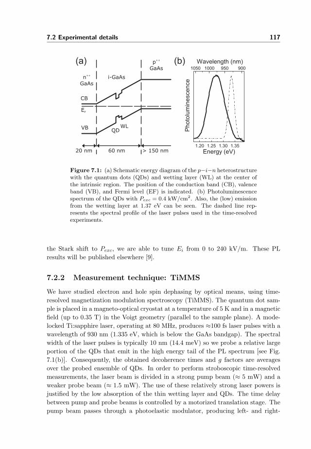
7.2 Experimental details 117
1.20 1.25 1.30 1.35
1050 1000 950 900
Ph
oto
lum
ine
sce
nce
Energy (eV)
Wavelength (nm)
i-GaAs
p
GaAs
++
n
GaAs
++
CB
VB
EF
QDWL
20 nm 60 nm > 150 nm
(a) (b)
Figure 7.1: (a) Schematic energy diagram of the p−i−n heterostructurewith the quantum dots (QDs) and wetting layer (WL) at the center ofthe intrinsic region. The position of the conduction band (CB), valenceband (VB), and Fermi level (EF) is indicated. (b) Photoluminescencespectrum of the QDs with Pexc = 0.4 kW/cm2. Also, the (low) emissionfrom the wetting layer at 1.37 eV can be seen. The dashed line rep-resents the spectral profile of the laser pulses used in the time-resolvedexperiments.
the Stark shift to Pexc, we are able to tune Ei from 0 to 240 kV/m. These PLresults will be published elsewhere [9].
7.2.2 Measurement technique: TiMMS
We have studied electron and hole spin dephasing by optical means, using time-resolved magnetization modulation spectroscopy (TiMMS). The quantum dot sam-ple is placed in a magneto-optical cryostat at a temperature of 5 K and in a magneticfield (up to 0.35 T) in the Voigt geometry (parallel to the sample plane). A mode-locked Ti:sapphire laser, operating at 80 MHz, produces ≈100 fs laser pulses with awavelength of 930 nm (1.335 eV, which is below the GaAs bandgap). The spectralwidth of the laser pulses is typically 10 nm (14.4 meV) so we probe a relative largeportion of the QDs that emit in the high energy tail of the PL spectrum [see Fig.7.1(b)]. Consequently, the obtained decoherence times and g factors are averagesover the probed ensemble of QDs. In order to perform stroboscopic time-resolvedmeasurements, the laser beam is divided in a strong pump beam (≈ 5 mW) and aweaker probe beam (≈ 1.5 mW). The use of these relatively strong laser powers isjustified by the low absorption of the thin wetting layer and QDs. The time delaybetween pump and probe beams is controlled by a motorized translation stage. Thepump beam passes through a photoelastic modulator, producing left- and right-
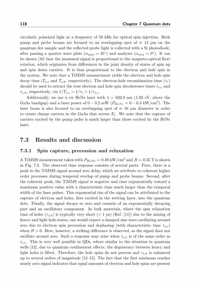
118 Chapter 7 Quantum dots
circularly polarized light at a frequency of 50 kHz for optical spin injection. Bothpump and probe beams are focused to an overlapping spot of ≈ 12 µm on thequantum dot sample and the reflected probe light is collected with a Si photodiode,after passing a quarter wave plate (αqwp = 45◦) and analyzer (αana = 0◦). It canbe shown [10] that the measured signal is proportional to the magneto-optical Kerrrotation, which originates from differences in the joint density of states of spin upand spin down carriers. It is thus proportional to the electron and hole spin inthe system. We note that a TiMMS measurement yields the electron and hole spindecay time (Ts,e and Ts,h, respectively). The electron-hole recombination time (τr)should be used to extract the true electron and hole spin decoherence times τs,e andτs,h, respectively, via 1/Ts,e = 1/τr + 1/τs,e.
Additionally, we use a cw HeNe laser with λ = 632.8 nm (1.92 eV, above theGaAs bandgap) and a laser power of 0− 3.2 mW (PHeNe = 0− 0.4 kW/cm2). Thelaser beam is also focused to an overlapping spot of ≈ 16 µm diameter in orderto create charge carriers in the GaAs that screen Ei. We note that the capture ofcarriers excited by the pump pulse is much larger than those excited by the HeNelaser.
7.3 Results and discussion
7.3.1 Spin capture, precession and relaxation
A TiMMS measurement taken with PHeNe = 0.38 kW/cm2 and B = 0.35 T is shownin Fig. 7.2. The observed time response consists of several parts. First, there is apeak in the TiMMS signal around zero delay, which we attribute to coherent higherorder processes during temporal overlap of pump and probe beams. Second, afterthe coherent peak, the TiMMS signal is negative and rises exponentially toward amaximum positive value with a characteristic time much larger than the temporalwidth of the laser pulses. This exponential rise of the signal can be attributed to thecapture of electron and holes, first excited in the wetting layer, into the quantumdots. Finally, the signal decays to zero and consists of an exponentially decayingpart and an oscillatory component. In bulk materials, where the spin relaxationtime of holes (τs,h) is typically very short (< 1 ps) (Ref. [11]) due to the mixing ofheavy and light hole states, one would expect a damped sine wave oscillating aroundzero due to electron spin precession and dephasing (with characteristic time τs,e)when B > 0. Here, however, a striking difference is observed, as the signal does notoscillate around zero. Such a response may arise when τs,h is of the same order asτs,e. This is very well possible in QDs, where similar to the situation in quantumwells [12], due to quantum confinement effects, the degeneracy between heavy andlight holes is lifted. Therefore, the hole spins do not precess and τs,h is enhancedup to several orders of magnitude [13–15]. The fact that the first minimum reachesnearly zero signal indicates that equal amounts of electron and hole spins are present
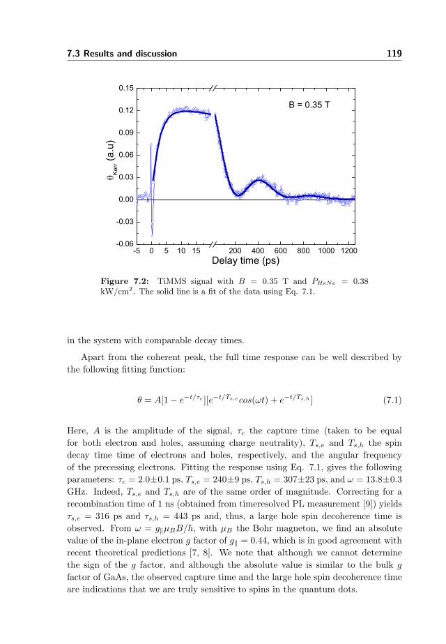
7.3 Results and discussion 119
-5 0 5 10 15 200 400 600 800 1000 1200-0.06
-0.03
0.00
0.03
0.06
0.09
0.12
0.15
B = 0.35 T
Ker
r (a.u
)
Delay time (ps)
Figure 7.2: TiMMS signal with B = 0.35 T and PHeNe = 0.38kW/cm2. The solid line is a fit of the data using Eq. 7.1.
in the system with comparable decay times.
Apart from the coherent peak, the full time response can be well described bythe following fitting function:
θ = A[1− e−t/τc ][e−t/Ts,ecos(ωt) + e−t/Ts,h ] (7.1)
Here, A is the amplitude of the signal, τc the capture time (taken to be equalfor both electron and holes, assuming charge neutrality), Ts,e and Ts,h the spindecay time time of electrons and holes, respectively, and the angular frequencyof the precessing electrons. Fitting the response using Eq. 7.1, gives the followingparameters: τc = 2.0±0.1 ps, Ts,e = 240±9 ps, Ts,h = 307±23 ps, and ω = 13.8±0.3GHz. Indeed, Ts,e and Ts,h are of the same order of magnitude. Correcting for arecombination time of 1 ns (obtained from timeresolved PL measurement [9]) yieldsτs,e = 316 ps and τs,h = 443 ps and, thus, a large hole spin decoherence time isobserved. From ω = g‖µBB/~, with µB the Bohr magneton, we find an absolutevalue of the in-plane electron g factor of g‖ = 0.44, which is in good agreement withrecent theoretical predictions [7, 8]. We note that although we cannot determinethe sign of the g factor, and although the absolute value is similar to the bulk g
factor of GaAs, the observed capture time and the large hole spin decoherence timeare indications that we are truly sensitive to spins in the quantum dots.
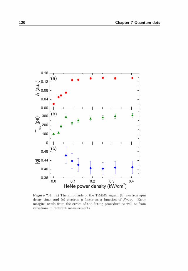
120 Chapter 7 Quantum dots
0.00
0.04
0.08
0.12
0.16
(c)
(b)
A (a
.u.)
(a)
0
100
200
300
T s,e (p
s)
0.0 0.1 0.2 0.3 0.40.36
0.40
0.44
0.48
HeNe power density (kW/cm2)
|g|
Figure 7.3: (a) The amplitude of the TiMMS signal, (b) electron spindecay time, and (c) electron g factor as a function of PHeNe. Errormargins result from the errors of the fitting procedure as well as fromvariations in different measurements.
7.4 Conclusion 121
7.3.2 Electric field dependence
We have performed similar measurements as a function of PHeNe, from which wehave extracted the amplitude A of the TiMMS signal, the electron spin decay timeτe and the in-plane electron g factor g‖, as shown in Fig. 7.3. Discussion of the holespin decay times is beyond the scope of this paper. We note that in the analysis ofsome measurements, we omitted the exponential rise part of Eq. 7.1. We observethat A strongly depends on PHeNe [Fig. 7.3(a)], rising from 0.02 at low PHeNe (highEi ) to 0.14 when Ei is fully quenched. A similar dependence on PHeNe is found forτe. These observations can be attributed to the increased loss of electron spin dueto tunneling of electrons from the QDs to the GaAs at high Ei. As shown in Fig.7.1, at high Ei, a triangular barrier between the QDs and the GaAs exists throughwhich electrons can tunnel. As it is difficult to correct for the exact contribution oftunneling, we cannot conclude that the observed decrease in τe indicates a decreasein the electron spin decoherence time τse. Figure 7.3(c) shows the dependence ofthe electron g factor on PHeNe. Although the uncertainty in the determination ofg‖ is rather large as a result of the combination of relative low B and small g‖, theseresults indicate a slight increase of g‖ from 0.40± 0.03 at high PHeNe to 0.46± 0.04at smaller PHeNe (thus, increasing Ei). It is known that the electron g factor canchange when the overlap of the wavefunction with the surrounding material changes,however, it is not trivial to predict what the change will be for these particular QDs.
7.4 Conclusion
In conclusion, we have performed time-resolved magneto-optical measurements ona single layer of selfassembled (In,Ga)As/GaAs QDs as a function of the built-inelectric field Ei. We have observed electron spin precession and large hole spindecoherence times in the QDs. The decrease of the observed electron spin decaytime with increasing Ei can be attributed to enhanced tunneling of electrons out ofthe QDs. Also, we have observed a slight increase of the electron in-plane g factorfrom 0.40± 0.03 to 0.46± 0.04 with increasing Ei, however, additional experimentsare needed to fully resolve the behavior of g‖ at high Ei.
Note added
We already mentioned that the electronic properties of quantum dots, and in par-ticular the electron and hole g factors, depend strongly on the size and shape ofthe dots. According to calculations of Pryor and Flatte, for InAs self-assembleddots with a circular base, a height of ≈ 3 nm, and an optical gap of 1.3 eV, theelectron g factor is close to +0.4, while the hole g factor is close to −0.15, for bothin-plane directions. These calculation also show that dots with increased heightshow a decreased magnitude of electron g factors, and an increased magnitude ofthe hole g factors. Elongation of the base of the dot has a more rigorous effect
122 Chapter 7 Quantum dots
on the hole g factor, indicated by a change from −0.15 to −0.8 when the aspectratio of the elliptical base is increased from 1 to 1.4 (again for an optical gap of 1.3).Further analysis of the atomic force microscopy images of the samples in the presentstudy revealed an average dot elongation of about 1.6. Together with an averagedot height of ≈ 6− 7 nm, this could imply a higher magnitude of the hole g factorcompared to the electron g factor. If this is the case, the correct interpretation ofthe experimental data presented in this Chapter is that the observed precession isin fact precession of the hole spin. In Figures 7.2 and 7.3, the labels for electronand hole should then be interchanged.
BIBLIOGRAPHY 123
Bibliography
[1] Z. Yuan, B. E. Kardynal, R. M. Stevenson, A. J. Shields, C. J. Lobo, K. Cooper,N. S. Beattie, D. A. Ritchie, and M. Pepper, Electrically Driven Single-PhotonSource, Science 295, 102 (2002). 7.1
[2] D. Loss and D. P. DiVincenzo, Quantum computation with quantum dots, Phys.Rev. A 57, 120 (1998). 7.1
[3] G. Salis, Y. Kato, K. Ensslin, D. C. Driscoll, A. C. Gossard, and D. D.Awschalom, Electrical control of spin coherence in semiconductor nanostruc-tures, Nature (London) 414, 619-622 (2001). 7.1
[4] Y. Kato, R. C. Myers, D. C. Driscoll, A. C. Gossard, J. Levy, and D. D.Awschalom, Gigahertz electron spin manipulation using voltage-controlled g-tensor modulation, Science 299, 1201-1204 (2003). 7.1
[5] T. Nakaoka, T. Saito, J. Tatebayashi, S. Hirose, T. Usuki, N. Yokoyama, and Y.Anakawa, Tuning of g factor in self-assembled In(Ga)As quantum dots throughstrain engineering, Phys. Rev. B 71, 205301 (2005). 7.1
[6] M. F. Doty, M. Scheibner, I. V. Ponomarev, E. A. Stinaff, A. S. Bracker, V. L.Korenev, T. L. Reinecke, and D. Gammon, Electrically Tunable g Factors inQuantum Dot Molecular Spin States, Phys. Rev. Lett. 97, 197202 (2006). 7.1
[7] C. E. Pryor and M. E. Flatte, Lande g Factors and Orbital Momentum Quench-ing in Semiconductor Quantum Dots, Phys. Rev. Lett. 96, 026804 (2006). 7.1,7.3.1
[8] W. Sheng and A. Babinski, Zero g factors and nonzero orbital momenta inself-assembled quantum dots, Phys. Rev. B 75, 033316 (2007). 7.1, 7.3.1
[9] G. W. W. Quax, All-optical control of the g factor in self-assembled(In,Ga)As/GaAs quantum dots, Ph.D. Thesis, Eindhoven University of Tech-nology, Eindhoven, The Netherlands (2008). 7.2.1, 7.3.1
[10] B. Koopmans, M. van Kampen, and W. J. M. de Jonge, Electron and Hole SpinDynamics in Magnetic Semiconductors, Phys. Status Solidi B 215, 217 (2000).7.2.2
[11] D. J. Hilton and C. L. Tang, Optical Orientation and Femtosecond Relaxationof Spin-Polarized Holes in GaAs, Phys. Rev. Lett. 89, 146601 (2002). 7.3.1
[12] R. W. Martin, R. J. Nicholas, G. J. Rees, S. K. Haywood, N. J. Mason, and P.J. Walker, Two-dimensional spin confinement in strained-layer quantum wells,Phys. Rev. B 42, 9237-9240 (1990). 7.3.1
124 Chapter 7 Quantum dots
[13] K. Gundogdu, K. C. Hall, E. J. Koerperick, C. E. Pryor, M. E. Flatte, T. F.Boggess, O. B. Shchekin, and D. G. Deppe, Electron and hole spin dynamicsin semiconductor quantum dots, Appl. Phys. Lett. 86, 113111 (2005). 7.3.1
[14] S. Laurent, B. Eble, O. Krebs, A. Lemaıtre, B. Urbaszek, X. Marie, T. Amand,and P. Voisin, Electrical Control of Hole Spin Relaxation in Charge TunableInAs/GaAs Quantum Dots, Phys. Rev. Lett. 94, 147401 (2005).
[15] L. M. Woods, T. L. Reinecke, and R. Kotlyar, Hole spin relaxation in quantumdots, Phys. Rev. B 69, 125330 (2004). 7.3.1
[16] J. Pingenot, C. E. Pryor, and M. E. Flatte, Method for full Bloch sphere controlof a localized spin via a single electrical gate, Appl. Phys. Lett. 92, 222502(2008).
Summary
Spin dynamics in hybrid spintronic devices andsemiconductor nanostructures
The research described in this Thesis is positioned in the field of Spintronics. Theaim of this research field is to enable spin-based electronics (in contrast to contem-porary charge based electronics), which should lead to improved device performanceand new device functionalities. A well known example of a spintronics device is thegiant magnetoresistive sensor used in computer hard disk drives to read the mag-netic information. The development of this sensor followed only ten years after thediscovery of the giant magnetoresistance (GMR) effect, a discovery which has beenawarded with the Nobel Prize in physics in 2007. Another example of a spintronicdevice is the magnetoresistive random access memory (MRAM), which has the po-tential to become a universal non-volatile memory. In order to fully exploit thespin degree of freedom in conventional semiconductor devices, one has to be able toinject, manipulate, transport, and detect a spin polarization in a semiconductor sys-tem. In conventional semiconductors (such as silicon or gallium arsenide), a createdspin polarization will not last forever as a result of several spin scattering mecha-nisms. Therefore, only a limited amount of time is available for spin manipulationand transport, which is essential for obtaining device functionality. Knowledge andcontrol of the dynamic properties of spin in (hybrid) semiconductor devices is thusessential.
In this Thesis we have used time-resolved microscopic optical techniques to studyspin and magnetization dynamics in hybrid spintronic devices and semiconductornanostructures. The technique involves a so-called pump-probe scheme, in whichthe system under investigation is perturbed by a pump pulse, and in which theresponse of the system to this perturbation is measured by an optical probe pulse.In order to study magnetization dynamics in a ferromagnetic layer, the pump pulseis a magnetic field pulse, and the perturbation is measured via the magneto-opticalKerr-effect of the optical probe pulse. In case of semiconductor materials, the pumppulse is an optical pulse which creates a non-equilibrium spin polarization, whilethe evolution of this spin polarization is measured via (again) the magneto-opticalKerr-effect.
125
126 Summary
The basics of magnetization dynamics, and spin relaxation and precession aredescribed in Chapter 2 of this Thesis. Also, we discuss the implications of opticalexcitation in the medium to high fluence regime on the spin dynamics. A detaileddescription of the experimental magneto-optical techniques is given in Chapter 3. Inorder to interpret the magneto-optical Kerr-signal originating from magnetic mul-tilayers, and semiconductor heterostructures, we have performed a detailed anal-ysis, thereby accounting for multiple interface reflections and the photon energyof the laser light. We discuss the applicability of the magneto-optical techniquesand analysis with illustrative examples, such as the development of perpendicularlymagnetized electrodes for spin injection, a system of two cobalt-platinum multilayerblocks suited for demagnetization experiments, and spin relaxation, precession anddiffusion in a lateral spin injection device.
The main systems investigated in this Thesis are presented and discussed in thenext Chapters, and involve a building block for an MRAM, a spin light-emittingdiode, GaAs based nanowires, and (In,Ga)As quantum dots.
Chapter 4 presents spatio-temporal measurement of the magnetization dynam-ics in the free-magnetic layer of an MRAM-element. The observation of a non-uniform magnetization precession, in the form of the occurrence of localized modesat the edges of the micron sized element, implies an obstacle for uniform preces-sional switching of the magnetization. It is shown that the presence of a significantstrayfield from the pinned layer is responsibly for these localized modes, and thatthis strayfield manifests itself in the domain structure of the magnetization of thefree layer.
The dependence of the electron spin relaxation rate on the current through aspin-LED is investigated in Chapter 5. The main observation is a current-inducedincrease of the electron spin relaxation rate. Detailed measurements as a function ofcurrent, laser fluence, laser photon energy, and spatial position, together with devicesimulations, give a non-trivial picture of the spin relaxation in the spin-LED. Thedominant contribution to the current-induced increase of the electron spin relaxationrate is by an increased hole density and temperature via the Bir-Aronov-Pikus spinflip mechanism.
In Chapter 6 the carrier and spin dynamics in GaAs-based nanowires is investi-gated. Spectroscopic measurements on an ensemble of multi-segmented GaP-GaAsnanowires show a rapid recombination rate of the optically excited carriers. Thisrapid recombination rate is attributed to a strong non-radiative recombination viadefect or surface states, as a result of the large surface-to-volume ratio of these wires.It is shown that the experimental technique is capable of performing measurementson individual GaP-GaAs-GaP nanowires, and that it is possible to study a singlesegment of such a nanowire. Measurements on several nanowires show again a rapidrecombination rate, while the spin lifetime seems to be limited by this rapid re-combination. This limits the accurate determination of the intrinsic spin relaxationmechanisms.

Summary 127
The influence of an internal electric field on the g factor of electron and holes ina single layer of self-assembled (In,Ga)As quantum dots is the topic of Chapter 7.Measurement of spin relaxation and precession as a function of the internal electricfield, show a decreasing spin lifetime and a small increase of the g factor when theinternal electric field increases. Increasing tunnel probabilities of carriers out of thequantum dots at high internal electric field, and changing carrier wavefunctions dueto a different confinement potential might explain these effect. These results mightenable g factor (and thereby) spin manipulation in such quantum dots.

128 Summary
Samenvatting
Spin dynamics in hybrid spintronic devices andsemiconductor nanostructures
Het onderzoek beschreven in dit proefschrift kan worden ondergebracht in het onder-zoeksgebied ‘Spintronica’. Dit onderzoeksgebied bestudeert en zoekt naar toepassin-gen die gebruik maken van de ‘spin’ van het electron. Het elektron zelf is het el-ementaire deeltje met een elektrische lading waarop de hedendaagse elektronica isgebaseerd. Een electron is echter ook een klein magneetje: het heeft een magnetischmoment dat ‘spin’ genoemd wordt. Het actieve gebruik van deze ‘spin’ in nieuwe‘spintronische’ apparaatjes (ofwel devices), zal leiden tot betere prestaties en nieuwefunctionaliteiten. Een zeer bekend ‘spintronisch’ device is de zogenaamde reuzen-magneto-weerstand sensor, die gebruikt wordt in de leeskop van harde schijven voorhet lezen van de magnetische informatie. De ontwikkeling van deze revolutionairesensor volgde slechts tien jaar na de ontdekking van het reuzen-magneto-weerstandeffect, een ontdekking die bekroond is met de Nobelprijs voor de natuurkunde in2007. Deze sensor heeft de stormachtige groei van de opslagcapaciteit van een hard-disk gedurende het afgelopen decennium mogelijk gemaakt. Een ander voorbeeldis het magnetische random-access-memory, dat in de toekomst mogelijk een uni-verseel niet-vluchtig geheugen zal vormen, waardoor de soms lange opstarttijd vaneen computer tot het verleden behoort.
Om de ‘spin’ van het electron volledig uit te buiten in huidige en toekomstigehalfgeleider devices, moeten een aantal problemen worden opgelost. Deze bestaanonder andere uit het injecteren van een significante hoeveelheid ‘spin’ (ook wel spinpolarisatie) in een halfgeleider, en het transporteren, manipuleren, en detecteren vandeze spin-polarisatie. In de meest gebruikte halfgeleiders zoals silicium en galliumarsenide (GaAs), verdwijnt deze spin-polarisatie zeer snel, in typisch een miljardstevan een seconde, door allerlei spin-relaxatie mechanismen. Hierdoor is er maareen beperkte tijd beschikbaar voor het uitvoeren van spin manipulatie en transport,terwijl dit essentieel is voor het maken van een werkend en functioneel device. Kennisvan en controle over de dynamische eigenschappen van ‘spin’ in halfgeleider devices(of in halfgeleider-metaal, de zogenaamde hybride devices) is dus essentieel.
129
130 Samenvatting
Voor het onderzoek beschreven in dit proefschrift, is gebruikt gemaakt van eentijd-, plaats- en spectraal opgeloste optische techniek om de dynamica van ‘spin’en magnetisatie (de geordende spins in een magnetisch materiaal) te bestuderen inhybride spintronische devices en in halfgeleider nanostructuren. Deze stroboscopis-che techniek werkt volgens het pump-probe principe. Hierbij wordt een systeemverstoord (‘gepompt’) door een ‘pump’-puls en wordt deze verstoring gemeten dooreen ‘probe’-puls, waarbij de tijd tussen ‘pump’ en ‘probe’ puls nauwkeurig gecon-troleerd kan worden tot beneden de picoseconde (een miljoenste van een miljoenstevan een seconde). Om de magnetisatie dynamica te meten in een ferromagnetischelaag, wordt als pomp een magnetische veld puls gebruikt en wordt de respons van demagnetisatie gemeten met een laser puls via het magneto-optische Kerr-effect. Omspin dynamica in halfgeleiders te meten, wordt als pomp een laser puls gebruikt dieeen spin polarisatie creeert in de halfgeleider. Het verval en gedrag van deze spinpolarisatie wordt wederom gemeten met een laser puls via het magneto-optischeKerr-effect.
Na een introductie van het onderzoeksgebied Spintronica, wordt in Hoofdstuk 2van dit proefschrift een beschrijving gegeven van magnetisatie dynamica in ferro-magnetische materialen, en van spin dynamica in halfgeleiders. Met name de spinrelaxatie mechanismen in GaAs komen aan bod en de implicaties van spin relax-atie en precessie in n−gedoteerd GaAs na optische excitatie met een relatief sterkelaser puls worden met enkele numerieke modellen uitgewerkt. In Hoofdstuk 3 wor-den de experimentele technieken in detail beschreven, waarbij het magneto-optischeKerr-effect een centrale rol inneemt. Met name wordt aandacht besteed aan deanalyse van het Kerr-effect dat afkomstig is uit magnetische multilagen en halfgelei-der heterostructuren, waarbij rekening wordt gehouden met meervoudige grensvlakreflecties en de golflengte van de laser pulse. Met enkele illustratieve voorbeelden(zoals de ontwikkeling van loodrecht gemagnetiseerde electroden voor spin injectie,een systeem van twee blokken met cobalt-platina multilagen voor demagnetisatieexperimenten, en spin relaxatie, precessie en diffusie in een lateraal spin injectiedevice) wordt de kracht van deze technieken en analyse toegelicht.
De belangrijkste devices en structuren die in het kader van dit proefschrift zijnonderzocht, worden gepresenteerd in de Hoofdstukken 4 tot en met 7. Het betrefthier een bouwsteen van een magnetisch geheugen, een spin-LED, halfgeleider nan-odraden gemaakt van GaAs, en zogenaamde quantum dots bestaande uit een mixvan indium arsenide en gallium.
Hoofdstuk 4 beschrijft de tijd- en plaats-opgeloste metingen van de magnetisatiedynamica in de vrije laag van een magnetische tunneljunctie (met afmetingen van13 bij 9 micrometer), die een bouwsteen vormt van een magnetisch geheugen. Dezemetingen laten een niet-uniforme respons van de magnetisatie op een magnetischeveld puls zien. De precessie van de magnetisatie die volgt op deze magnetische pulsheeft aan de randen van de vrije laag een andere frequentie en uitdoving dan inhet midden van het element. Dit gedrag bemoeilijkt het snel uniform precessioneel
Samenvatting 131
switchen van de magnetisatie van de vrije laag. Aangetoond wordt dat de oorzaakvan dit gedrag het magnetisch strooiveld afkomstig van de niet-vrije laag van detunneljunctie is, en dat dit strooiveld ook de domein structuur van de vrije beınvloed.
In Hoofdstuk 5 wordt aangetoond dat de effectiviteit van de spin relaxatie vanelektronen in de actieve laag van een spin-LED toeneemt met de stroom door dezespin-LED. Gedetailleerde experimenten, waarbij zowel de stroom, het laser vermo-gen, de golflengte van de laser, en de plaats op de spin-LED zijn gevarieerd, latenzien dat de dominante bijdrage aan de toegenomen effectiviteit van spin relaxatiekan worden toegeschreven aan een verhoogde gaten-dichtheid en temperatuur inde active laag van de spin-LED. Het relaxatie-mechanisme dat hiervoor zorgt ishet zogenaamde Bir-Aronov-Pikus-mechanisme. Deze waarnemingen zijn in goedeovereenstemming met numerieke simulaties van de stroom, gaten-dichtheid, en tem-peratuur van de spin-LED.
De dynamica van ladingsdragers en spins in halfgeleider nanodraden gebaseerdof GaAs wordt besproken in Hoofdstuk 6. Spectroscopische metingen aan een groteverzameling nanodraden bestaande uit segmenten van gallium fosfide (GaP) enGaAs laten een zeer snelle recombinatie zien van ladingsdragers na optische ex-citatie met een laser puls. Deze zeer snelle recombinatie wordt toegeschreven aaneen sterke niet-stralende recombinatie aan defecten in het rooster of aan het opper-vlak van de nanodraden, tengevolge van de grote oppervlakte-volume verhouding.Gedemonstreerd wordt dat de experimentele techniek het mogelijk maakt om metin-gen te verrichten aan individuele nanodraden, en dat zelfs een enkel segment in eenGaP-GaAs-GaP nanodraad kan worden geıdentificeerd. Metingen aan verscheidenenanodraden laten wederom een zeer snelle recombinatie van ladingsdragers zien.Magneto-optische metingen duiden op een spin levensduur die gelimiteerd wordtdoor deze snelle recombinatie, wat een nauwkeurige meting van de intrinsieke spinlevensduur bemoeilijkt.
In Hoofdstuk 7 wordt de invloed van een intern elektrisch veld op de spin relax-atie en de g factor van elektronen en gaten in een enkele laag van zelf-samengestelde(In,Ga)As quantum dots onderzocht. Het actief kunnen veranderen van de g factormoet het mogelijk maken om spins in quantum dots te kunnen manipuleren. Metin-gen van de spin relaxatie en precessie als functie van het intern elektrisch veld,laten zien dat de spin levensduur verminderd en de g factor enigszins groter wordt,naarmate de sterkte van het intern elektrisch veld stijgt. Deze afhankelijkheid vanhet elektrisch veld kan mogelijk worden toeschreven aan een veranderende opsluit-ingspotentiaal van ladingsdragers in de quantum dot, en aan veranderde waarschi-jnlijkheden voor ladingsdragers om uit de quantum dot te tunnelen.

132 Samenvatting
List of publications
J. H. H. Rietjens, C. A. C. Bosco, P. Van Dorpe, W. Van Roy, and B. KoopmansCurrent-induced increase of the electron spin relaxation rate in a spin-LEDIn preparation
J. H. H. Rietjens, C. A. C. Bosco, M. T. Borgstrom, E. P. A. M. Bakkers, and B.KoopmansProbing carrier and spin dynamics in GaAs-based nanowiresIn preparation
G. Malinowski, F. Dalla Longa, J. H. H. Rietjens, P. V. Paluskar, R. Huijink, H. J.M Swagten, and B. KoopmansControl of speed and efficiency of ultrafast demagnetization by direct transfer of spinangular momentumNat. Phys. 4, 855 (2008).
J. H. H. Rietjens, G. W. W. Quax, C. A. C. Bosco, R. Notzel, A. Yu. Silov, and B.KoopmansOptical control over electron g factor and spin decoherence in (In,Ga)As/GaAsquantum dotsJ. Appl. Phys. 103, 07B116 (2008)
G. W. W. Quax, T. E. J. Campbell Ricketts, A. M. Yakunin, T. van Lippen, R.Notzel, P. M. Koenraad, C. A. C. Bosco, J. H. H. Rietjens, B. Koopmans, and A.Yu. SilovAll-optical control of the exciton g-factor in InAs/GaAs quantum dotsPhyica. E 40, 1832-1835 (2008)
J. H. H. Rietjens, C. Jozsa, H. Boeve, W. J. M. de Jonge, and B. KoopmansEffect of stray field on local spin modes in exchange-biased magnetic tunnel junctionelementsAppl. Phys. Lett. 87, 172508 (2005)
133

134 List of publications
J. H. H. Rietjens, C. Jozsa, H. Boeve, W. J. M. de Jonge, and B. KoopmansProbing local spin modes in exchange-biased MTJ elementsJ. Magn. Magn. Mater. 290, 494-497 (2005).
C. Jozsa, J. H. H. Rietjens, M. van Kampen, E. Smalbrugge, M. K. Smit, W. J. M.de Jonge, and B. KoopmansRetrieving pulse profiles from pump-probe measurements on magnetization dynam-icsJ. Appl. Phys. 95, 7447 - 7449 (2004)
About the author
Jeroen Henricus Hubertus Rietjens was born on October 18th 1978 in Weert, theNetherlands. He grew up in Nederweert and attended the Philips van Horne Sc-holengemeenschap in Weert, where he received his VWO-diploma in June 1997.
Between September 1997 and April 2004 he studied Applied Physics at the Eind-hoven University of Technology (TU/e). He did internships at the group Plasma andMaterials Processing (TU/e), Vanderlande Industries, and at the Institute for As-tronomy in Honolulu, Hawaii. His final project was carried out in the group Physicsof Nanostructures (TU/e), and concerned precessional magnetization dynamics inmicron sized ferromagnetic elements. He received is Master in Applied Physics (cumlaude) in April 2004, and was awarded the Mignot Award for best master thesis ofthe Eindhoven University of Technology of 2004.
Between April 2004 and December 2008 he has been working as a PhD-candidatein the group Physics of Nanostructures (TU/e) on a research project within theNanoNed initiative. His research focused on the magnetization and spin dynamicsin hybrid spintronic devices and semiconductor nanostructures. This work has ledto several publications in renowned scientific journals and presentations at interna-tional conferences.
Besides his professional activities, he has been a member of the board of the study-association for Applied Physics “Johannes Diderik van der Waals”, and is at presentSecretary of VENI, the alumni-association of Applied Physics in Eindhoven, andTreasurer of Stichting Natuurkunst, a foundation whose main activity was the real-ization of a grand public artwork, SOH19 States of Nature, at the entrance of thecampus of the TU/e.
135

136
Dankwoord
Met deze laatste woorden van mijn proefschrift wil ik graag iedereen bedanken dieop zijn of haar manier een bijdrage heeft geleverd aan het totstandkomen van ditwerk.
In het bijzonder gaat mijn dank uit naar mijn promotoren, Bert Koopmans enHenk Swagten, en commissielid Wim de Jonge. Zij hebben niet alleen deze pro-motieplaats mogelijk gemaakt, maar ook gezorgd voor goede begeleiding, aanstur-ing, kritische vragen, op de juiste momenten gezonde motiverende prikkels, en nietin de laatste plaats voor de fantastische sfeer in de groep Fysica van Nanostructuren.Het zijn deze zaken die mij houvast hebben geboden en mij in staat hebben gesteldom mijn promotieonderzoek tot een goed einde te brengen.
Bert, bedankt voor je vertrouwen, je enthousiasme en geduld, je grondige kennisen het bijna altijd vinden van antwoorden en mogelijke oplossingen op mijn vragenover theorie en experiment. Het was een eer om in jouw groep te mogen werken, ikheb er ontzettend veel van geleerd. Henk, bedankt voor je adviezen en luisterendoor, zowel in N-laag als af en toe in de trein naar Weert, zowel met betrekking totmijn onderzoek als (ver) daarbuiten en voor de goede correcties en suggesties bij hetschrijven van dit proefschrift. Wim, bedankt voor je interesse in mijn onderzoek ende soms confronterende (maar wel noodzakelijke) vragen tijdens de werkbesprekin-gen. De gesprekken over de meest uiteenlopende zaken die volgden op het ‘evengoedendag zeggen’ vormden een welkome afleiding. Het was me een genoegen me temogen verdiepen in de meest onwaarschijnlijke problemen met computers en internetdie alleen jou leken te overkomen.
Bedankt ook mijn co-promotor Erik Bakkers en Magnus Borgstrom van PhilipsResearch voor de samenwerking op het gebied van halfgeleider nanodraden, metname voor het leveren van de samples en voor verhelderende discussies. Hetzelfdegeldt voor Wim Van Roy, Pol Van Dorpe en Reinier Vanheertum van IMEC Leu-ven, voor de samenwerking met de spin-LED en de spin injectie devices, en voorGuido Quax en Andrei Silov voor het quantum dot project. Deze samenwerkingenhebben mij de mogelijkheid geboden om met systemen te werken die niet binnen degroep FNA vervaardigd konden worden en hebben in alle gevallen geleid tot mooieresultaten en vormen ieder een essentieel onderdeel van dit proefschrift.
De nog niet genoemde commissieleden Andrea Fiore, Paul van Loosdrecht en
137
138 Dankwoord
Gerd Bacher wil ik danken het plaatsnemen in de promotiecommissie en voor hetkritisch lezen van mijn proefschrift.
Vanzelfsprekend gaat veel dank uit naar iedereen van de groep FNA voor hetvormen van een gezonde werkomgeving, de sportieve afleiding met zaal- en veld-voetbal, en de gezelligheid in de koffiekamer tijdens de pauze, Sinterklaas-, Kerst-en champagnepartijtjes en tijdens groepsuitjes en conferenties. Jurgen, Oleg, Ger-rie, Jef en Jeroen, bedankt voor jullie assistentie bij experimenten en technischeproblemen. Karin, bedankt voor al het administratieve werk en de vele op maatgesneden adviezen met betrekking tot het gezinsleven. Uiteraard gaat mijn dankuit naar de promovendi en post-docs met wie ik gedurende mijn verblijf in de groepFNA heb gewerkt: de laserlabpers Carlos, Francesco, Greg en Csaba, de groeiersParesh, Jurgen, Corine, Reinoud en Coen, de molecuulmannen Francisco en Wiebe,de NMR-ers Sabine en Harm, de STM-ers Muriel en Omer, en de schrijvers van2004 Veronica, Karel en Corne.
Van de vele afstudeerders en stagiaires die in de groep FNA hebben gewerkt, gaatmijn speciale dank uit naar Sebastiaan Rieter, Paul Claassen, William Hermkens,Wim van Hemmen en Joost van Bree. Het was me een genoegen om jullie te mogenbegeleiden en te profiteren van het vele goede werk dat jullie hebben verricht.
Tijdens mijn promotieonderzoek ben ik ook vele malen geholpen door personenbuiten de groep FNA. Met name wil ik Marius, Han, Henk, Frank, Ginny en Marcovan de werkplaats, Rens, Toon en Marieke van de receptie, en Karin Raijmakers enJan Millenaar graag hartelijk bedanken voor de meest uiteenlopende hulp.
Natuurlijk ben ik ook veel dank verschuldigd aan personen die de gedurendemijn promotieonderzoek mijn zogenaamde neven- en sociale activiteiten tot eenwaar plezier hebben gemaakt en daarmee ook voor motivatie en inspiratie voor mijnonderzoek hebben gezorgd.
In het bijzonder wil ik alle (bestuurs)leden van Stichting Natuurkunst bedankenvoor de prettige samenwerking en het gigantisch mooie resultaat dat we samenhebben bereikt en dat hopelijk tot in de lengte van dagen te aanschouwen zal zijnop de campus van de TU/e. Ook de bestuursleden van alumnivereniging VENI(Saskia, Jan-Jaap, Igor, Sonja, Erik, Patrick, Wiebe, Daniel en Thijs) dank ik voorde vele gezellige vergaderingen en het goede werk dat we samen hebben verricht. Veeldank aan de Heeren van Evolutie voor vele ontspannende en hilarische momententijdens uitstapjes, etentjes en andere activiteiten. Hetzelfde geldt voor de ledenvan Stiefelcommissie Natuurkunde, met name tijdens het befaamde Stiefelweekend.Dank ook aan mijn teamgenoten van Eindhoven AV3/4 (het spijt me dat mijn knietot tweemaal toe roet in het eten heeft gegooid), en aan de Snarfjes, Aanhangsnarfjesen Babysnarfjes.
Tenslotte wil ik mijn grote dank uitspreken aan mijn familie, die gedurende mijngehele onderzoeksperiode, maar zeker ook in de laatste fase een enorme steun zijngeweest. Mijn ouders Henk en Corry, mijn zus Ellen en Wilfred, mijn schoonoudersWiel en Lenie en schoonbroer Hubert, heel, heel veel dank. Femke, ook tot jou

Dankwoord 139
wil ik nog enkele woorden richten. Jouw komst was een moment was een momentvan grote blijdschap, het was heerlijk om je te zien opgroeien en te zien spelen metHuub. De klap van jouw verlies zullen we misschien nooit te boven komen, vergetenzal ik je in ieder geval nooit.
Als allerlaatste gaat mijn dank uit naar degenen die het dichtst bij mij staan.Willy, ik kan onmogelijk in woorden uitdrukken hoeveel je voor me betekent enhoeveel steun ik aan je heb gehad. We hebben gedurende de tijd van mijn pro-motieonderzoek vele grote stappen gezet die onze relatie alleen maar hebben verri-jkt. Samen met Huub en Guus, die ons iedere dag weer laten beseffen hoe gelukkigwe zijn en die de gouden gave bezitten om op willekeurige momenten met een on-schuldige opmerking, handeling of boevenstreek een lach op ons gezicht te toveren,zie ik de toekomst vol vertrouwen tegemoet.
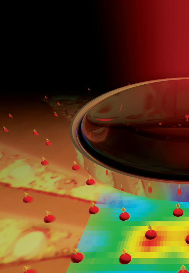


![arXiv:2002.08678v2 [cond-mat.mtrl-sci] 14 Jun 2020 · 2020. 6. 16. · based spintronic devices. PACS numbers: Spin-orbit coupling (SOC) is the quantum effect of rel-ativistic nature,](https://static.fdocuments.us/doc/165x107/612db7ba1ecc515869425cf9/arxiv200208678v2-cond-matmtrl-sci-14-jun-2020-2020-6-16-based-spintronic.jpg)