Spectroscopy and ab initio studies of optical transitions ...
13
Spectroscopy and ab initio studies of optical transitions in nanostructured ZnO R. Plugaru a) , A. Dinescu a) , F. Comanescu a) , M. Purica a) , S. Mihaiu b) , E. Vasile c) , F. Babarada d) , N. Plugaru e) a) National Institute for Research and Development in Microtechnologies-IMT Bucharest b) Institute of Physical Chemistry "I.G. Murgulescu" Romanian Academy c) METAV S.A.-CD, Bucharest d) University “Politehnica” Bucharest e) National Institute for Materials Physics, Bucharest-Magurele Project 11-048/2007 NANOXI
Transcript of Spectroscopy and ab initio studies of optical transitions ...

Spectroscopy and ab initio studies of optical transitions in
nanostructured ZnO
R. Plugarua), A. Dinescua), F. Comanescua), M. Puricaa), S. Mihaiub), E. Vasilec), F. Babaradad), N. Plugarue)
a) National Institute for Research and Development in Microtechnologies-IMT Bucharestb) Institute of Physical Chemistry "I.G. Murgulescu" Romanian Academy c) METAV S.A.-CD, Bucharestd) University “Politehnica” Buchareste)National Institute for Materials Physics, Bucharest-Magurele
Project 11-048/2007 NANOXI

Layout
• Overview• Experimetal
SynthesisXRD, SEM, TEMUV-VIS and Fluorescence Spectroscopy
• DFT study• Conclusions
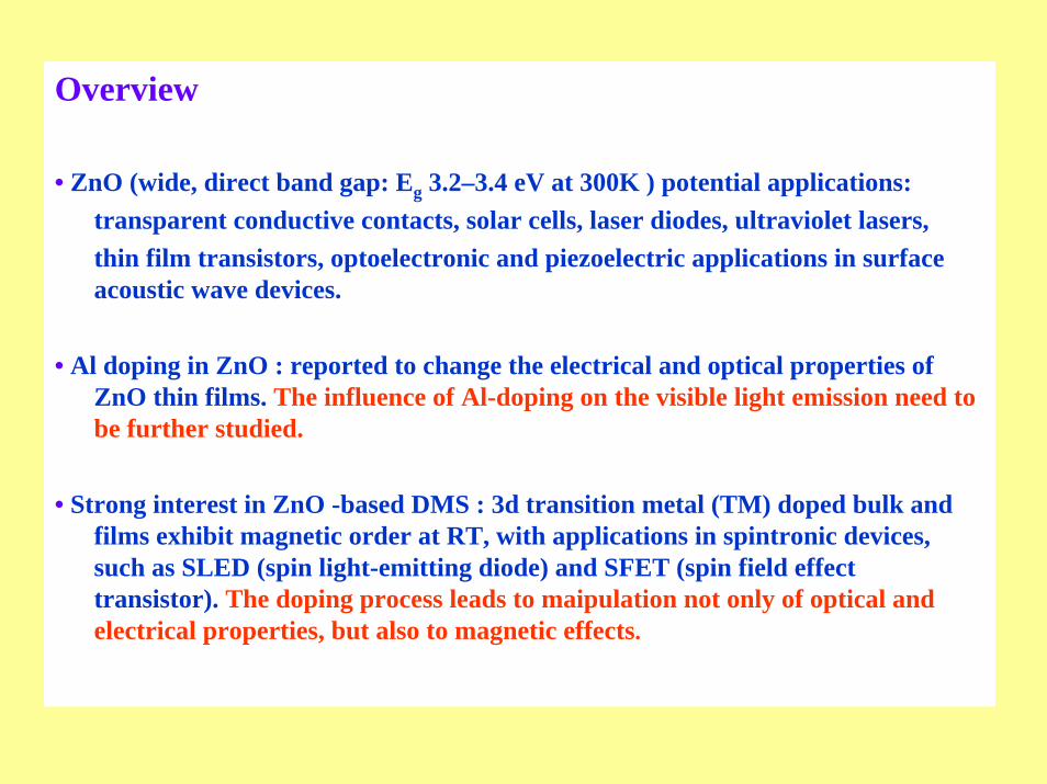
Overview
• ZnO (wide, direct band gap: Eg 3.2–3.4 eV at 300K ) potential applications: transparent conductive contacts, solar cells, laser diodes, ultraviolet lasers, thin film transistors, optoelectronic and piezoelectric applications in surface acoustic wave devices.
• Al doping in ZnO : reported to change the electrical and optical properties of ZnO thin films. The influence of Al-doping on the visible light emission need to be further studied.
• Strong interest in ZnO -based DMS : 3d transition metal (TM) doped bulk and films exhibit magnetic order at RT, with applications in spintronic devices, such as SLED (spin light-emitting diode) and SFET (spin field effect transistor). The doping process leads to maipulation not only of optical and electrical properties, but also to magnetic effects.

Synthesis of ZnO:Al layers (0.5% and 5%Al)0.05M ZAD in
Absolute Ethanol
Stirring at 60 0C15 min
TEA TEA / Zn=1:5 molar ratio
Stirring at 50 0C105 min
A3+ solutionZn/Al =19:1 atomic ratio
Clear and homogeneous sol
Dip Coating
Glass andSi/SiOx substrates
Repeating
After 24 h
Preheating at 500 0C for 5 min
Annealing at 500 0C for 1h
Al doped-ZnO
0.05M ZAD in Absolute Ethanol0.05M ZAD in
Absolute Ethanol
Stirring at 60 0C15 min
Stirring at 60 0C15 min
TEA TEA / Zn=1:5 molar ratio
TEA TEA / Zn=1:5 molar ratio
Stirring at 50 0C105 min
Stirring at 50 0C105 min
A3+ solutionZn/Al =19:1 atomic ratio
A3+ solutionZn/Al =19:1 atomic ratio
Clear and homogeneous solClear and homogeneous sol
Dip Coating
Glass andSi/SiOx substrates
Repeating
After 24 h
Preheating at 500 0C for 5 minPreheating at 500 0C for 5 min
Annealing at 500 0C for 1h
Al doped-ZnO
•Sol-gel method on Si/SiO2 and glass.
•Multilayers : n = 1 - 10 layers
•Thickness: ~10 nm/ layer
Solutions prepared from: • Zinc acetate dihydrate (p.a ):
Zn(CH3COO)2x2H2O (ZAD)• Aluminiumnitrat-nonahydrat:
Al(NO3)3·9H2O(ANN)• absolute ethanol - CH3CH2OH• Triethanolamine - (CH3CH2OH)3N (TEA)
DTG, DTA and TG analysis of Al doped ZnO gel.
Preparation procedure of ZnO:Al multilayers by sol-gel process.

XRD and SEMSi/SiO2 Glass
200 nm
SEM images of the surface of ZnO:0.5%Al 10 layers films grown on Si/SiO2 and glass substrates.
XRD patterns of ZnO:0.5%Al, 5 layers and 10 layers on Si/SiO2 and glass substrates.

HRTEMSi/SiO2 Glass
HRTEM images and corresponding SAED patterns of ZnO:0.5%Al 10 layers films grown on Si/SiO2 and glass substrates.

UV-VIS Spectroscopy
0
10
20
30
40
50
60
70
80
90
100
190 290 390 490 590 690 790 890
Wavelength [nm]
Tran
smitt
ance
[%]
10 layers ZnO:0.5%Al
4 layers ZnO
4 layers ZnO:5%Al
0
10
20
30
40
50
60
70
80
90
100
190 290 390 490 590 690 790 890
Wavelength [nm]
Tran
smitt
ance
[%]
10 layers
1 layer treated
1 layer untreated
Optical transmission of ZnO, ZnO:0.5%Al and ZnO:5% Al layers.
0
0,4
0,8
1,2
1,6
2
200 300 400 500 600 700 800 900
Wavelength [nm]
Abs
orba
nce
[a.u
.]
10 layers ZnO:0.5%Al4 layers ZnO:0.5%Al1 layer ZnO:0.5%Al
0
0,4
0,8
1,2
1,6
2
200 300 400 500 600 700 800 900
Wavelength [nm]
Abs
orba
nce
[a.u
.]
4 layers ZnO:5%Al4 layers ZnO:0.5%Al4 layers ZnO
UV–VIS absorption spectra of ZnO, ZnO:0.5%Al and ZnO:5%Al layers.

Fluorescence
Fluorescence properties of ZnO and ZnO:0.5%Al layers grown on Si/SiO2 and glass substrates, at an excitation wavelength of 350 nm.
300 350 400 450 5000
50
100
150
200
250
300
350
400
450
500
Inte
nsity
[a.u
.]
Wavelength [nm]
1 layer ZnO 3 layers ZnO 4 layers ZnO
300 350 400 450 500 550 600
0
20
40
60
80
100
120
Inte
nsity
[a.u
.]
Wavelength [nm]
1 layer ZnO untreated 1 layer ZnO treated 2 layers ZnO 3 layers ZnO 4 layers ZnO
350 400 450 500 550 6000
100
200
300
400
500
λex=350 nm
Inte
nsity
[a.u
.]
Wavelength [nm]
1 layer ZnO:0.5% Al untreated 1 layer ZnO:0.5% Al treated 2 layers ZnO:0.5% Al 3 layers ZnO:Al 0.5% Al 4 layers ZnO:Al 0.5% Al 5 layers ZnO:Al 0.5% Al 10 layers ZnO:Al 0.5 l
350 400 450 500 550 600
0
20
40
60
80
100
120
140
160
λex=350 nm
Wavelength [nm]
Inte
nsity
[a.u
.] 1 layer ZnO:0.5 % Al untreated 1 layer ZnO:0.5% Al treated 2 layers ZnO:0.5% Al 3 layers ZnO:0.5% Al 4 layers ZnO:0.5% Al 5 layers ZnO:0.5% Al 10 layers ZnO:0.5% Al
387nm383nm386nm383nm
Absorption and fluorescence emission in the bulk ZnO and nc ZnO.[N. Goswami, D.K. Sharma / Physica E 42 (2010) 1675–1682]

Raman Spectroscopy

DFT study
L(S)DA and LSDA+U, CPA-FPLO code [1].
- wurtzite-type Zn1-xTMxO (TM= Al, Ti, Mn) x= 2, 5 and 10 %- substitutional disorder at Zn site.- no lattice relaxation ==> only electronic effects.
Al:ZnO

Ti:ZnO Mn:ZnO

Table 1. Magnetic moment per 3d ion, m, and per formula unit, M, in Ti/Mn:ZnO.
----------------------------------------------------------------------------------x (3d) (at.%) 2 5 10
------------------------------------------------------------------------------------m (μB/at) Ti 0.90 1.13 1.28
Mn 4.71 4.71 4.71
M (μB/f.u.) Ti 0.02 0.06 0.13
Mn 0.10 0.25 0.50-----------------------------------------------------------------------------------

Conclusions• Al-doped ZnO multilayered films with hexagonal wurtzite structure were grown by sol-gel route on Si/SiO2 and glass substrates.
• The substrate effect on films structure: a) Si/SiO2 substrate : nanostructured ZnO:0.5% at.Al layers (crystallites of 3-15 nm) with preferential (002) orientation; b) Glass substrate : nanostructured ZnO:0.5at%Al (crystallites of 6-10 nm) randomly oriented.
• Thickness of 10 layers : about 100 nm. The ZnO crystal structure could be observed starting with 4-5 layers deposition.
• The transmittance of the 1-10 layers of ZnO:0.5at%Al is in the range of 80%-90% in the visible and near infra-red regions.
• Fluorescence emission shows the presence of defects, interstitial Zn, OVs.
• The optical band edge of ZnO is shifted to a shorter wavelength when increasing Al concentration (blue shift). Optical transmittance spectra and Moss–Burstein theory..
• Ab-initio calculations predict : i) Al, Ti, Mn behave as donors; ii) different effects on conductivity and magnetism; iii) local magnetic moments in T and Mn:ZnO.