Spectrometer gratings based on direct-write e-beam lithography
26
U.D . Zeitner, T. Flügel - Paul, T. Harzendorf , M. Heusinger, E. - B. Kley Fraunhofer Institut für Angewandte Optik und Feinmechanik Jena, Germany 10. October 2017 Spectrometer gratings based on direct-write e-beam lithography 3μm Electron-beam lithography for grating fabrication Examples of astro-gratings: CUBES UV-transmission grating CarbonSat high-resolution gratings Sub- structures for ultra-wide-band gratings
Transcript of Spectrometer gratings based on direct-write e-beam lithography
U.D. Zeitner, T. Flügel-Paul, T. Harzendorf,
M. Heusinger, E.-B. KleyFraunhofer Institut für Angewandte Optik und Feinmechanik
Jena, Germany
10. October 2017
Spectrometer gratings based on
direct-write e-beam lithography
3µm
Electron-beam lithography for grating fabrication
Examples of astro-gratings:
CUBES UV-transmission grating
CarbonSat high-resolution gratings
Sub- structures for ultra-wide-band gratings

High Performance Applications of Gratings
Spectrometers for Astronomy
and Earth Observation
relevant parameters:
spectral dispersion
bandwidth
efficiency / polarization
wavefront
straylight
size, …
often extreme demands
to obtain required performance
Manipulation/Compression of
Ultra-Short Laser Pulses
chirped Pulse
compressed
Pulse
Sentinel 4 (ESA)

1. Resist exposure with
e-beam lithography
Grating Technology at the IOF
2. Resist development
3. Chromium etching
(RIE)
4. Deep etching into
substrate (ICP)
resist
Cr-layer
SiO2-Substrate
e-
optional:
multiple iterations
of the process for
multi-level elements5. Removal of Cr-layer

HR layer
stack
substrate
grating
0th order
-1st order
1µm
Gratings on dielectric layer stacks
• highly efficient reflection gratings
• transmission gratings with tailored polarization properties

SB350 OS
(Vistec)
The Vistec SB350 OS e-beam writer
max. writing field: 300mm x 300mm
max. substrate thickness: 15mm
resolution (direct write): <50nm
address grid: 1nm
stitching error: < 12nm P-V / < 2.2nm RMS
placement error: < 14nm P-V
writing strategy: variable shaped beam /
cell projection
huge flexibility to
tailor the structure
parameters!
angular
apertures
e-beam
electron opticsvery fast
writing process!

+ 6.3nm
- 6.6nm
19mm
50m
m
wavefront placement
PV 12.8nm <10.3 nm
rms 1.4nm <1.1 nm
wave-front measurement(1µm period grating + technology, Littrow-Mount)
position [mm]
pe
rio
d v
aria
tio
n [p
m]
- Asphere-Test CGH
- Puls compression gratings
- Spectrometer gratings (space application)
Applications requiring
this accuracy
period variation < 5 pm
Key Performance: Writing Accuracy

Accuracy of writing process: straylight
0 2 4 6 8 10
10-2
10-1
100
101
102
BS
DF
[sr-1
]
[°]
20140711 #22 8Pass, Std I
20130917 FIMAS_uze147e_3
Wein-Formula with =2nm
Optimization of e-beam writing process
optimized writing process
significant reduction of
peak number and intensity
FIMAS EBB
reflex from
substrate
angle wrt. -1st diffraction order
BSDF of -1st DO:
51526 sr -1
conventional e-beam
writing process
Examples of realized
spectrometer gratings

CUBES – UV Transmission Grating
CUBES (Cassegrain U-Band Brazilian ESO-Spectrograph
Requirements:
• spectral band: 300nm – 400nm
• line density: 3448 lines/mm p=290nm
• AOI: 31°
• grating size: 250 x 250 mm² ; mosaic of 2x [250mm x 130mm]
Challenges:
• commercial VPH gratings difficult in the UV
Solution:
• Binary fused silica gratings
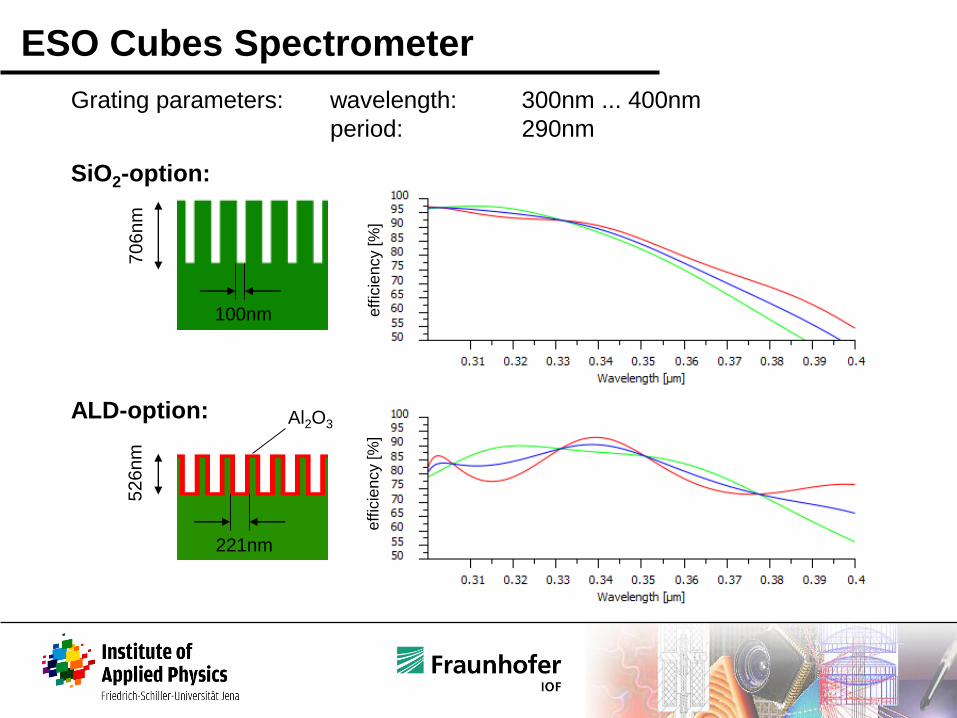
ESO Cubes Spectrometer
Grating parameters: wavelength: 300nm ... 400nm
period: 290nm
ALD-option:
SiO2-option:
706nm
100nm
526nm
221nm
eff
icie
ncy [%
]e
ffic
iency [%
]
Al2O3
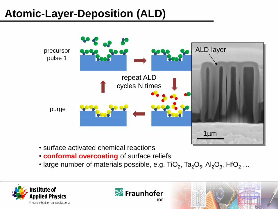
precursor
pulse 1purge
purge
precursor
pulse 2
repeat ALD
cycles N times
• surface activated chemical reactions
• conformal overcoating of surface reliefs
• large number of materials possible, e.g. TiO2, Ta2O5, Al2O3, HfO2 …
Atomic-Layer-Deposition (ALD)
1µm
ALD-layer

CUBES – UV Transmission Grating
realized grating during efficiency
measurement
grating size: 250mm x 130mm
design
best fit of measurement data

Tiling for Larger Gratings
arrangement of 2 reflection gratings
(420mm x 210mm)
active alignment for
wave-front optimization
single grating
210mm x 210mm
also possible for
transmission gratings
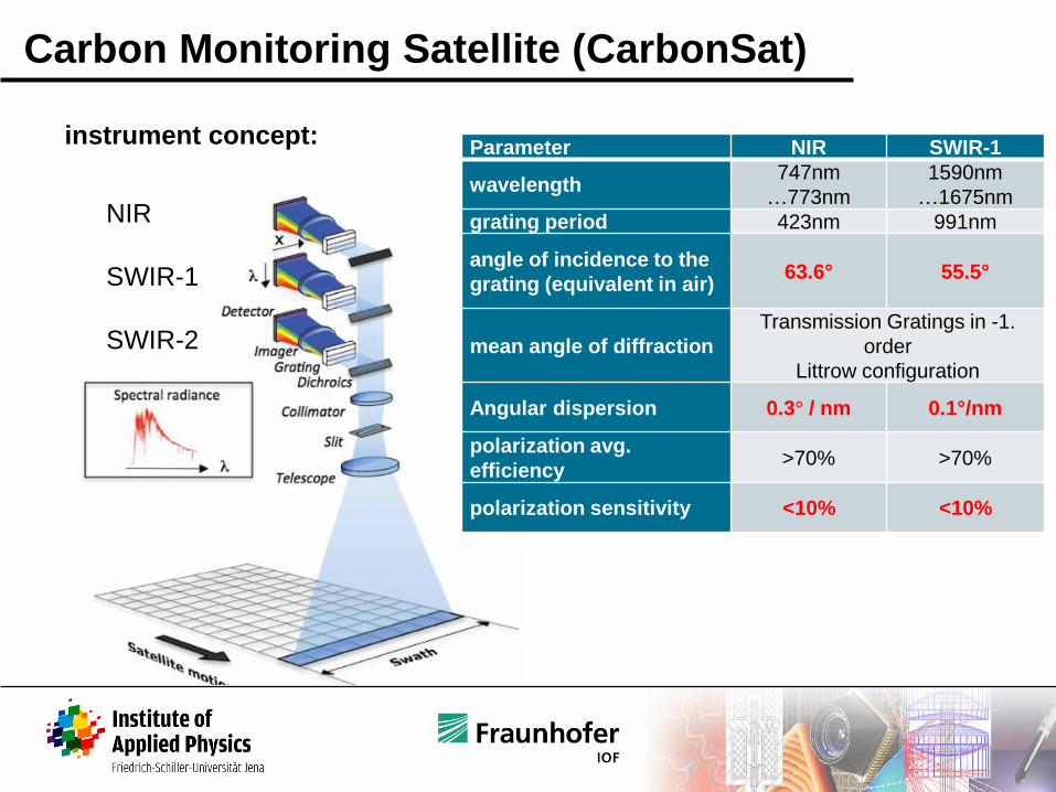
Parameter NIR SWIR-1
wavelength747nm
…773nm
1590nm
…1675nm
grating period 423nm 991nm
angle of incidence to the
grating (equivalent in air)63.6° 55.5°
mean angle of diffraction
Transmission Gratings in -1.
order
Littrow configuration
Angular dispersion 0.3° / nm 0.1°/nm
polarization avg.
efficiency>70% >70%
polarization sensitivity <10% <10%
Carbon Monitoring Satellite (CarbonSat)
instrument concept:
NIR
SWIR-1
SWIR-2
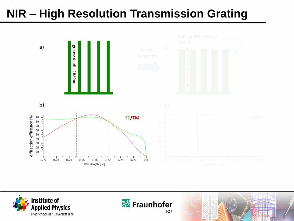
NIR – High Resolution Transmission Grating

NIR – High Resolution Transmission Grating
use high-refractive-index (dielectric) coating to reduce depth

Optical Performance
NIR-grating
SWIR-1-grating
AOI: 64°
AOI: 55°

Direct Glass-to-Glass Bonding
• achieved alignment accuracy: 0.25mrad (< 1 arcmin)
• bond strength up to 2/3 of bulk fused silica
• current TRL: 6
Advantages: adhesive free glass-to-glass connection
no additional optical interface
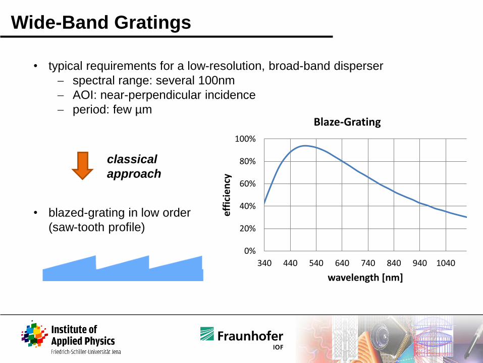
Wide-Band Gratings
• blazed-grating in low order
(saw-tooth profile)
classical
approach
• typical requirements for a low-resolution, broad-band disperser
spectral range: several 100nm
AOI: near-perpendicular incidence
period: few µm
0%
20%
40%
60%
80%
100%
340 440 540 640 740 840 940 1040
effi
cie
ncy
wavelength [nm]
Blaze-Grating

Echelle or Echellette Structures
Electron Beam Lithography
Ion Beam Etching of Mask
Wet Chemical Etching of Silicon
„Blaze Angle“ can be adjusted by crystalline orientation
of Silicon substrate

Echelle or Echellette Structures
period = 2µmperiod = 30µm
also lower line
densities possible
currently shown on 6” size substrates
(up to 12” possible)
integrated cross-
dispersion grating
by direct-write
structuring

Alternative: Effective Index Gratings
sub-wavelength pattern with varying fill factor
Ph. Lalanne et al. 1998
Advantages: only one lithography step
tailoring of dispersion properties
=
blazed grating local effective index
local fill-factor variationsub-wavelength
structures

Effective Medium Gratings
grating period
top view
FLEX (fluorescence explorer);
[500nm – 800nm]GAIA (global astrometic interferometer
for astrophysics); [750nm – 800nm]
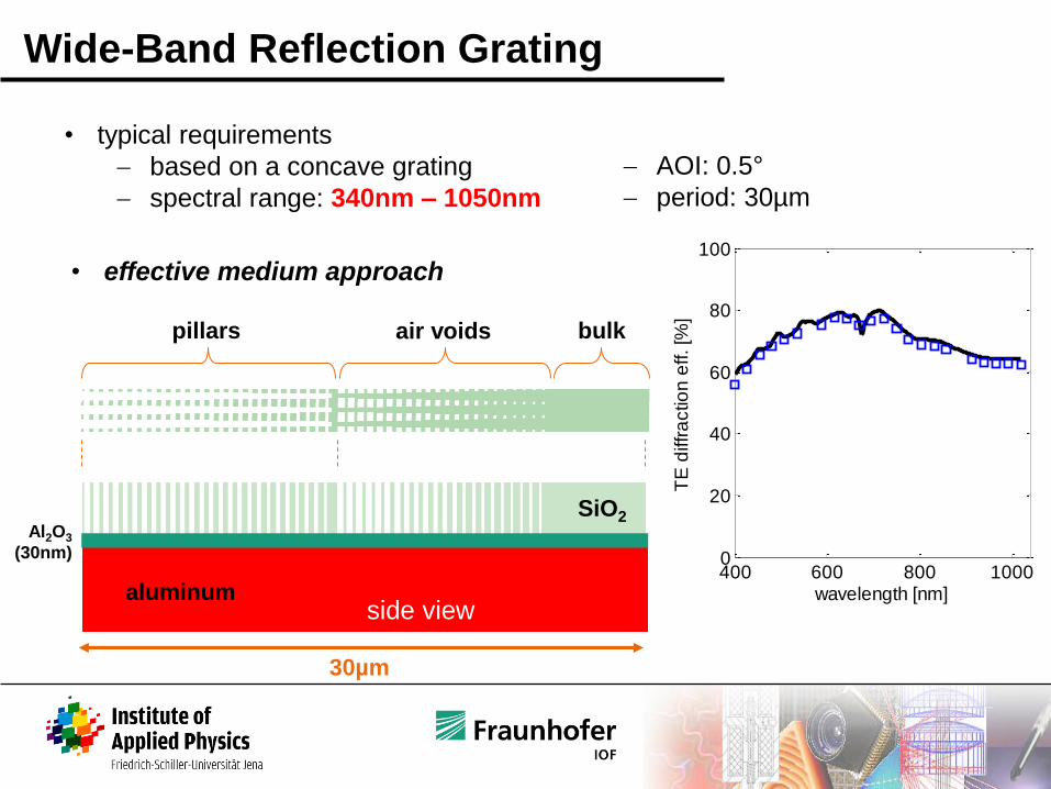
Wide-Band Reflection Grating
• typical requirements
based on a concave grating
spectral range: 340nm – 1050nm
side view
top view
30µm
pillars air voids bulk
aluminum
SiO2Al2O3
(30nm)
AOI: 0.5°
period: 30µm
• effective medium approach
400 600 800 10000
20
40
60
80
100
wavelength [nm]
TE
diffr
actio
n e
ff. [%
]
400 600 800 10000
20
40
60
80
100
wavelength [nm]
TM
diffr
actio
n e
ff. [%
]

Wide-Band Reflection Grating …
… realized by E-beam lithography
measured diffraction efficiency:
very weak spectral dependency of diffraction efficiency
including reduced UV
reflectivity of Al-layer

• Direct write electron-beam lithography has a huge potential for
the realization of high-performance gratings
• It offers a unique flexibility and the accuracy to meet even
extreme requirements
• Atomic-Layer-Deposition (ALD) considerably extends the
flexibility to access the full potential of advanced grating designs
• Realization of GRISMs by direct bonding
• Examples are:
• high resolution gratings with low polarization sensitivity
• echelle-type gratings with integrated cross-disperser
• ultra-wide-band gratings for lower resolution spectrometers
Summary
Sub-period engineering by combining
E-Beam lithography and Atomic-Layer-Deposition
To make use of the large flexibility and the
advantageous optical properties requires talking with
the grating manufacturer already during the design of
the instrument !!!
(not after PDR…)
L
L

![2 LASER INTERFERENCE LITHOGRAPHY - uni-halle.de · 2 LASER INTERFERENCE LITHOGRAPHY (LIL) 9 2 LASER INTERFERENCE LITHOGRAPHY (LIL) Laser interference lithography [3~22] (LIL) is a](https://static.fdocuments.us/doc/165x107/5eae180eecc7e273a41a4e88/2-laser-interference-lithography-uni-hallede-2-laser-interference-lithography.jpg)