SPD CNC - Tapmatic
12
FYS 3180/4180 H-09 Department of Physics http://www.uio.no/studier/emner/matnat/fys/FYS3180/h09/ http://www.fys.uio.no/studier/kurs/fys3180/ Characterization of defects in proton-irradiated Si using deep level transient spectroscopy Prosjektoppgave i FYS3180/4180, Fall-2009 Physical Electronics Micro- and Nanotechnology Laboratory (MiNaLab) University of Oslo Abstract In this investigation, dominant crystal defects in high purity silicon material subjected to proton irradiation will be studied using electrical measurement techniques, especially deep level transient spectroscopy (DLTS). The crystal defects are of point like nature, with an extension of a few Å to 1 nm, and the majority of the defects are of vacancy type. The positions in the energy band gap of the electron states caused by these defects will be determined as well as the kinetics of the thermal stability of the defects. Finally, on the basis of these results, the radiation hardness of the silicon material will be estimated and compared with requirements in high energy physics experiments at the Large Hadron Collider (LHC) at CERN and in satellite (space) experiments. Content I. Introduction…………………………... p. 2 (a) Energy bands and defect states…… p. 2 (b) Emission and capture processes….. p. 4 II. Experimental…………......................... p. 6 (a) DLTS……………………………... p. 6 (b) Samples…………………………... p. 10 (c) Instrumentation………………….... p. 11 III. Definition of tasks……......................... p. 12 IV. References……………......................... p. 12 1
Transcript of SPD CNC - Tapmatic

FYS 3180/4180
H-09 Department of Physics http://www.uio.no/studier/emner/matnat/fys/FYS3180/h09/ http://www.fys.uio.no/studier/kurs/fys3180/
Characterization of defects in proton-irradiated Si using
deep level transient spectroscopy
Prosjektoppgave i FYS3180/4180, Fall-2009
Physical Electronics
Micro- and Nanotechnology Laboratory (MiNaLab) University of Oslo
Abstract
In this investigation, dominant crystal defects in high purity silicon material subjected to proton irradiation will be studied using electrical measurement techniques, especially deep level transient spectroscopy (DLTS). The crystal defects are of point like nature, with an extension of a few Å to 1 nm, and the majority of the defects are of vacancy type. The positions in the energy band gap of the electron states caused by these defects will be determined as well as the kinetics of the thermal stability of the defects. Finally, on the basis of these results, the radiation hardness of the silicon material will be estimated and compared with requirements in high energy physics experiments at the Large Hadron Collider (LHC) at CERN and in satellite (space) experiments.
Content I. Introduction…………………………... p. 2 (a) Energy bands and defect states…… p. 2 (b) Emission and capture processes….. p. 4 II. Experimental…………......................... p. 6 (a) DLTS……………………………... p. 6 (b) Samples…………………………... p. 10 (c) Instrumentation………………….... p. 11 III. Definition of tasks……......................... p. 12 IV. References……………......................... p. 12
1

I. Introduction
I.(a) Energy band structure and defect states in semiconductors
Semiconductor materials in use for electronic devices are normally crystalline in nature and
the most common ones, like silicon (Si), germanium (Ge) and gallium arsenide (GaAs), all
display a diamond structure. The diamond structure can be regarded as composed of two
partially overlapping face centred cubic structures with a single atom at each lattice point.
Figure 1 shows an example for Si, which is the dominant semiconductor since more than 40
years. Between the lattice atoms and electrons there is a superposition of periodic Coulomb
potentials from each lattice atom and the super-positioned potential exhibits the same
periodicity as the crystal structure. This periodic potential lowers the total energy of the
electrons in the crystal, leading to crystal binding, and the electrons are forced to assume
certain energies only. More specifically, an energy interval with no electron states allowed
emerges in materials with insulating and semiconducting properties. This energy interval is
labelled the energy band gap (Eg) and is schematically illustrated in Figure 2 (Eg≈1.11 eV for
silicon at room temperature). The semi-infinite interval of energies with a lower limit at the
upper edge of Eg is called the conduction band (Ec) and correspondingly, the energy interval
with an upper limit at the lower edge of Eg is called the valence band (Ev).
In reality, any semiconductor is not perfect and will contain defects and impurities, either
intentionally or unintentionally introduced. As a result, the crystalline periodicity is
interrupted and energy states may appear within Eg, which affect the electrical properties of
the semiconductor. A prime example is the introduction of group V impurities (P, As, Sb) or
Figure 1. Tetrahedron formed by a Si-atom (centre) and the bonds to its four nearest neighbours.
Figure 2. Simplified illustration of the energy band gap in a semiconductor[1]. Dark dots represent filled electron states and white dots show empty states (holes).
2

group III impurities (B, Al, Ga, In) on substitutional lattice sites in the silicon structure (so-
called doping). The former ones will give rise to shallow electron states in Eg with respect to
Ec and readily become positively ionized by thermal excitation of electrons to the almost
empty conduction band (n-type doping). Correspondingly, the group III elements will cause
shallow electron states in Eg with respect to Ev and readily become negatively ionized by
thermal excitation of electrons from the almost fully occupied valence band (p-type doping).
Consequently, the electrical conductivity of the Si material can be drastically changed, either
by current transport via the almost free electrons in the conduction band (n-type conductivity)
or via the valence electrons ‘jumping’ to nearby empty states, so-called holes (p-type
conductivity)[1]. In addition, native (intrinsic) crystalline defects and unintentionally
introduced residual impurities can appear in the material and some fundamental examples like
vacancies and self-interstitials are schematically illustrated in Figure 3.
In silicon, the main residual impurities are oxygen, carbon and hydrogen[2]. Especially,
oxygen can occur with high concentrations in as-grown single crystalline silicon material
(~1x1018 cm-3, compared to the atomic density of ~5x1022 cm-3) and these oxygen atoms
occupy normally a bond-centred interstitial configuration (Oi), as illustrated in some detail by
Figure 4(a). The Oi atoms do not give rise to any energy state in Eg but they are likely to
capture monovacancies (V’s) in order to release the crystal strain associated with the Oi
configuration. The resulting defect formed is shown in Figure 4(b) and is labelled the
vacancy-oxygen (VO) centre[3]. The VO centre contains two dangling bonds from the two
unsaturated Si atoms and an electron energy state appears at ~0.18 eV below Ec. Another
prominent defect in silicon is the divacancy centre (V2)[4] which consists of two V’s in
nearest neighbour lattice positions, as displayed in Figure 4(c). The V2 centre appears in
particular after a silicon material has been exposed to irradiation with energetic particles, like
protons and electrons in high energy physics experiments or in the Van Allen radiation belt,
Figure 3. Illustration of fundamental point defects; vacancy (top right), self-interstitial (bottom right), substitutional impurity (top left) and interstitial impurity (bottom left). Open circles illustrate crystal host atoms and filled dark circles indicate impurity atoms.
3

Figure 4. Visualization of the atomic structure of the Oi (a), VO (b) and V2 (c) defects.
EC
EV
0.23 eV
0.20 eV
0.43 eV
Electron and charge states for V2
Figure 5. Illustration of electron states and charge states for the V2 centre in silicon.
2-
-
0
+
and it causes three different electron states in Eg corresponding to four charge states of V2 (+,
0, -1, -2), as depicted in Figure 5.
I.(b) Emission and capture of electrons/holes by energy states in the band gap
Let us consider an electron state at an energy ET below Ec and with a concentration of NT.
Figure 6(a) shows the total ‘traffic’ of electrons and holes to and from this state. The rate of
emission of an electron to Ec and a hole to Ev are denoted by en and ep, respectively. The rate
of capture of an electron from Ec or a hole from Ev are ncn and pcp, respectively, where cn and
cp are the so-called capture coefficients, and n and p are the concentrations of electrons in the
conduction band and holes in the valence band, respectively.
4

Figure 6. The total ‘traffic’ of charge carriers to and from a state is shown in (a). The special case of recombination is given in (b), trapping and emission in (c), and generation in (d).
}ET
Three typical situations can be identified; first, as shown in Figure 6(b), a state may act as a
recombination centre for pairs of electrons and holes. Second, as shown in Figure 6(c), a state
can act as a trap, and trapping and emission of electrons (or holes) are the dominating
processes. Third, as shown in Figure 6(d), a state can act as a generation centre for pairs of
electrons and holes.
According to Shockley and Read[5], the capture coefficient for a state can be expressed as:
cn(p) = σn(p)vth
where σn(p) is the capture cross section for electrons (holes) and vth is the thermal velocity,
vth = (3kT/m*n(p))½
with m*n(p) as the effective mass for electrons (holes), T as the absolute temperature, and k as
Boltzmann’s constant.
For the emission rate, the following relation holds[5]:
en(p)(T) = vth σn(p)NC(V)exp(-ET/kT) (1)
where NC(V) is the effective density of states in the conduction (valence) band.
5

II. Experimental
II.(a) Sample analysis by deep level transient spectroscopy (DLTS)
DLTS is the main technique to be used for the sample analysis, and in this section a brief
introduction to the basic principles of DLTS is given. The technique was first introduced by
Lang in 1974[6] and from DLTS one can obtain information about energy positions of states
in the band gap, capture cross sections for electrons and holes, average concentration of
energy states (defects) as well as concentration-versus-depth profiles of the states. In
particular, a hallmark of DLTS is a very high sensitivity reaching detection limits on the order
of 10-5 relative to the doping concentration.
DLTS requires a good rectifying junction in a semiconductor material, either a pn-junction or
a Schottky barrier junction, and it is based on measurements of the junction capacitance. The
basic structure of a pn-junction is given in Figure 7, and with the junction is associated a
depletion region, W , which is depleted of free charge carriers (electrons and holes). As a
result of W , a capacitance, , builds up at the junction and is given by rC
WACr
ε= with )11(2
da
r
NNqVW +=
ε
where ε is the permittivity (dielectric constant) of the material, A is the diode area, is total
bias over the junction, q is the elementary charge, is the acceptor doping concentration
and is the donor concentration.
rV
aN
dN
normally used for DLTS
measurem r ents, and fo a
Figure 7. Schematics of a pn-junction showing the ionized and dopants in the p- and n-regions, respectively.
−aN +
dN
W denotes the depletion region.
In practice, an asymmetrically doped junction, like p+n ( >> ) or a Schottky junction, is
normally used for DLTS measurements and for a p+n-junction is simplified to
aN dN
rC
rC = r
d
VqNA2
ε .
6
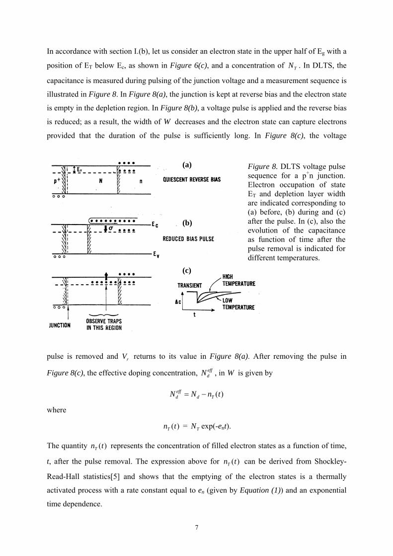
In accordance with section I.(b), let us consider an electron state in the upper half of Eg with a
position of ET below Ec, as shown in Figure 6(c), and a concentration of . In DLTS, the
capacitance is measured during pulsing of the junction voltage and a measurement sequence is
illustrated in Figure 8. In Figure 8(a), the junction is kept at reverse bias and the electron state
is empty in the depletion region. In Figure 8(b), a voltage pulse is applied and the reverse bias
is reduced; as a result, the width of
TN
W decreases and the electron state can capture electrons
provided that the duration of the pulse is sufficiently long. In Figure 8(c), the voltage
(a) Figure 8. DLTS voltage pulse sequence for a p+n junction. Electron occupation of state ET and depletion layer width are indicated corresponding to (a) before, (b) during and (c) after the pulse. In (c), also the evolution of the capacitance as function of time after the pulse removal is indicated for different temperatures.
(b)
(c)
pulse is removed and returns to its value in Figure 8(a). After removing the pulse in
Figure 8(c), the effective doping concentration, , in
rV
effdN W is given by
)(tnNN Tdeffd −=
where
)(tnT = exp(-ent). TN
The quantity represents the concentration of filled electron states as a function of time,
t, after the pulse removal. The expression above for can be derived from Shockley-
Read-Hall statistics[5] and shows that the emptying of the electron states is a thermally
activated process with a rate constant equal to en (given by Equation (1)) and an exponential
time dependence.
)(tnT
)(tnT
7

Hence, the capacitance after removing the pulse becomes
)(tC = r
Td
r
effd
VtnNqA
VqNA
2))((
2−
=εε
and assuming << one obtains: TN dN
)()( tCCtC r Δ−=
where
d
Tr
NNCtC
2)( =Δ exp(-ent).
The recovery of the capacitance as a function time occurs faster with increasing temperature,
as illustrated in Figure 8(c), and by taking the difference between and as a
function of temperature a DLTS spectrum is obtained, Figure 9. A maximum in the DLTS
signal occurs when the time interval - is on the order of the inverse rate constant (en)-1.
)( 1tC )( 2tC
2t 1t
Figure 9. Illustration of how a DLTS spectrum can be obtained. The left hand side shows )(tCCr Δ+ at various temperatures while the right hand-side shows the corre-sponding DLTS signal given by - as a function of temperature.
)( 1tC )( 1tC
8

In reality, the procedure outlined in Figure 9 for extracting the DLTS signal is rather sensitive
to noise in the capacitance measurements and instead, a sampling (weighting) function, ,
of the type shown in Figure 10 is frequently used. This sampling function is of lock-in type
and the DLTS signal, S(ti), is deduced according to
)(tw
S(ti) = ∫+
Δid
d
tt
ti
dttwtCt
)()(1
where td is a delay time of the capacitance meter. For td<<ti, S(ti) has a maximum amplitude
when
enti = 2.52
and the maximum value becomes
Smax = 0.102d
Tr
NNC .
Thus, can be deduced from Smax and by varying ti (the so-called time window) different
values of en at the peak maximum are obtained versus temperature. Then, by applying
Equation (1), ET and σn can be extracted using an Arrhenius plot provided that vth and NC are
known.
TN
Figure 10. Illustration of )(tCΔ and the use of a
sampling (weighting) function of lock-in type. )(tw
9

II.(b) Samples to be studied
All the samples to be used in this study are cut from a silicon wafer having a highly n-doped
(n+) substrate with a lightly n-doped (n-) epitaxial layer grown by chemical vapour deposition
at ITME[7], see the schematic in Figure 11(a). The wafers were subsequently processed by
SINTEF/MiNaLab into pads of p+-n--n+ diodes. The p+-layer was realized by ion implantation
of boron. The thickness of the epitaxial n--layer is ~20 µm and the doping concentration, ,
in the layer is about 3x1013 cm-3.
dN
After processing, rectangular samples with a size of about 2x2 mm2 were cut form the wafers,
and a photo of the processed and diced wafer is shown in Figure 11(b).
Finally, the samples were irradiated with 1.5 MeV protons at room temperature to doses
between 5x10⁹ and 6x10¹⁰ H+/cm2. The irradiations were undertaken at UiO/MiNaLab and the
samples have then been stored in a freezer at -20 °C.
(a) (b)
Figure 11. In (a), a schematic visualization of the p+-n--n+ samples is given. The front contact is the middle square, isolated by dark ditches of silicon dioxide (SiO2). The thickness of the epitaxial layer is about 20 µm with ≈3x1013 cm-3. The dimensions in (a) are not to scale. In (b), a photograph of a processed and diced wafer (∅ = 150 mm) is shown. The p+-n--n+ samples can be seen as small (2 mm)2 squares located in the areas that are covered with aluminium (grey). The rest of the structures on the wafer are irrelevant for this investigation.
dN
10

II.(c) Instrumentation for the measurements
The experimental setup to be used is designed for electrical measurements in the temperature
range from 77 K (LN2) to 400 K. The measurements include capacitance versus voltage and
current versus voltage and spectroscopic techniques like DLTS,. A block diagram of the
components in the setup and their interconnections is depicted in Figure 12 together with a
photograph of the sample cryostat. A core part of the setup is the capacitance meter
(HP4280A) which enables recording of capacitance transients, )(tCΔ , with a sampling rate of
1 MHz.
Figure 12. Block diagram of the DLTS setup to be used in this study. The photograph shows the sample cryostat and the LN2 Dewar.
11

III. Definition of tasks
• Determine the energy position and electron capture cross section of the dominant electron
states in the energy band gap of proton-irradiated high purity epitaxial silicon (n-type)
• Determine the concentration and generation rate of the dominant electron states as a
function of proton dose
• On the basis of comparison with literature data, identify the origin of the dominant
electron states
• Perform isothermal annealing studies to determine the thermal stability and annealing
kinetics of the dominant electron states
• Conclude about the radiation hardness of the investigated samples (devices/detectors) and
possibly predict their lifetime in (i) the Large Hadron Collider (LHC) at CERN and (ii) a
satellite exposed to the Van Allen radiation belt.
IV. References
[1] B.G. Streetman and S. Banerjee, Solid State Electronic Devices, Prentice Hall
International Inc., 6th edition (2006).
[2] See for example, M. Mikelsen, Thermal evolution of irradiation induced defects in Silicon
and Silicon Carbide, PhD thesis, University of Oslo (2007), and references therein.
[3] J.W. Corbett, G.D. Watkins, R.M. Chrenko and R.S. McDonald, Phys. Rev. 121, 1015
(1961); G.D. Watkins and J.W. Corbett, Phys. Rev. 121, 1001 (1961).
[4] J.W. Corbett and G.D. Watkins, Phys. Rev. Lett. 7, 314 (1961); G.D. Watkins and J.W.
Corbett, Phys. Rev. 138, A543 (1965).
[5] W. Shockley and W.T. Read, Phys. Rev 87, 835 (1952).
[6] D.V. Lang, J. Appl. Phys. 45, 3023 (1974).
[7] Institute of Electronic Materials Technology (ITME), Warszaw, Poland.
12