Sony Scd Xb940 Sm
73
SERVICE MANUAL SUPER AUDIO CD PLAYER AEP Model UK Model SPECIFICATIONS SCD-XB940 Model Name Using Similar Mechanism NEW CD Mechanism Type CDM55B-DVBU3 Base Unit Name DVBU3 Optical Pick-up Name KHM-220AAA/J1N – Continued on next page – Photo: Black type Ver 1.1 2002.05 9-929-212-12 Sony Corporation 2002E0500-1 Home Audio Company C 2002.05 Published by Sony Engineering Corporation
-
Upload
pietertje58 -
Category
Documents
-
view
53 -
download
2
description
Sony Scd Xb940 Sm
Transcript of Sony Scd Xb940 Sm

SERVICE MANUAL
SUPER AUDIO CD PLAYER
AEP ModelUK Model
SPECIFICATIONS
SCD-XB940
Model Name Using Similar Mechanism NEW
CD Mechanism Type CDM55B-DVBU3
Base Unit Name DVBU3
Optical Pick-up Name KHM-220AAA/J1N
– Continued on next page –
Photo: Black type
Ver 1.1 2002.05
9-929-212-12 Sony Corporation2002E0500-1 Home Audio Company
C 2002.05 Published by Sony Engineering Corporation

2
SAFETY-RELATED COMPONENT WARNING!!
COMPONENTS IDENTIFIED BY MARK 0 OR DOTTEDLINE WITH MARK 0 ON THE SCHEMATIC DIAGRAMSAND IN THE PARTS LIST ARE CRITICAL TO SAFEOPERATION. REPLACE THESE COMPONENTS WITHSONY PARTS WHOSE PART NUMBERS APPEAR ASSHOWN IN THIS MANUAL OR IN SUPPLEMENTS PUB-LISHED BY SONY.
Notes on chip component replacement• Never reuse a disconnected chip component.• Notice that the minus side of a tantalum capacitor may be dam-
aged by heat.
Flexible Circuit Board Repairing• Keep the temperature of the soldering iron around 270 ˚C dur-
ing repairing.• Do not touch the soldering iron on the same conductor of the
circuit board (within 3 times).• Be careful not to apply force on the conductor when soldering
or unsoldering.
CAUTIONUse of controls or adjustments or performance of proceduresother than those specified herein may result in hazardous ra-diation exposure.

3
TABLE OF CONTENTS
1. SERVICING NOTES ............................................... 4
2. GENERAL ................................................................... 5
3. DISASSEMBLY ......................................................... 8
4. DIAGRAMS4-1. Notes for Printed Wiring Board and
Schematic Diagram ......................................................... 114-2. Printed Wiring Board – TK Board – .............................. 124-3. Schematic Diagram – TK Board – ................................ 134-4. Printed Wiring Board
– MAIN Board (Component Side) – .............................. 144-5. Printed Wiring Board
– MAIN Board (Conductor Side) – ................................ 154-6. Schematic Diagram – MAIN Board (1/6) – .................. 164-7. Schematic Diagram – MAIN Board (2/6) – .................. 174-8. Schematic Diagram – MAIN Board (3/6) – .................. 184-9. Schematic Diagram – MAIN Board (4/6) – .................. 194-10. Schematic Diagram – MAIN Board (5/6) – .................. 204-11. Schematic Diagram – MAIN Board (6/6) – .................. 214-12. Printed Wiring Board – AUDIO Board – ...................... 224-13. Schematic Diagram – AUDIO Board – ......................... 234-14. Printed Wiring Board – HP Board – .............................. 244-15. Schematic Diagram – HP Board – ................................. 244-16. Printed Wiring Board – LOADING Board – ................. 254-17. Schematic Diagram – LOADING Board – ................... 254-18. Printed Wiring Board – DISPLAY Board – .................. 264-19. Schematic Diagram – DISPLAY Board – ..................... 274-20. Printed Wiring Board – POWER Board – ..................... 284-21. Schematic Diagram – POWER Board – ........................ 294-22. Printed Wiring Boards
– AC SW/TRANSFORMER Boards – ........................... 304-23. Schematic Diagram
– AC SW/TRANSFORMER Boards – ........................... 31
5. EXPLODED VIEWS ................................................ 36
6. ELECTRICAL PARTS LIST ............................... 40

4
The laser diode in the optical pick-up block may suffer electro-static break-down because of the potential difference generatedby the charged electrostatic load, etc. on clothing and the humanbody.During repair, pay attention to electrostatic break-down and alsouse the procedure in the printed matter which is included in therepair parts.The flexible board is easily damaged and should be handled withcare.
NOTES ON LASER DIODE EMISSION CHECKThe laser beam on this model is concentrated so as to be focusedon the disc reflective surface by the objective lens in the opticalpick-up block. Therefore, when checking the laser diode emis-sion, observe from more than 30 cm away from the objective lens.
MODEL IDENTIFICATION
– Back Panel –
SECTION 1SERVICING NOTES
NOTES ON HANDLING THE OPTICAL PICK-UPBLOCK OR BASE UNIT
Part No.
HOW TO OPEN THE TRAY WHEN POWER SWITCHTURNS OFFThere are two different methods to open the tray.
• Method-1Insert a screw driver (3) into the aperture of the unit bottom, andturn it in the direction of the arrow (to OUT direction).
tray
screw driver (3)
*To close the disc table, turn the screw driver (3) in the reverse direction (to IN direction).
Model Part No.
AEP 4-227-711-0s
UK 4-227-711-1s
tray
A
B
cam (CDM55)
screw driver (3)
• Method-2
1 Insert a screw driver (3) into the aperture of the unit bottom,and move the cam (CDM55) in the direction of arrow A.
2 Pull the tray in the direction of arrow B.
ABOUT THE “E01” DISPLAY“E01” is displayed when the above occurs in communication witha system controller (IC605) and a display controller (IC203) at thetime of starting.In this case, please check soldering, disconnection, etc. of eachIC.
Ver 1.1

5
SECTION 2GENERAL
This section is extracted frominstruction manual.
6

7

8
4 connector(CN992)
4 connector(CN351)
7 two claws
2 loading panel ass’y
qd front panel section
9 knob (AMS)
6 seven screws(BV/RING)
qa connector(CN201)
qs DISPLAY board
q; eight screws(BVTP2.6 × 8)
7 two claws
3 wire (flat type) (10 core)(CN601)
5 holder
1 Pull out the tray.(Refer to page 4, “HOW TO OPEN THETRAY WHEN POWER SWITCH TRANS OFF”.)
q; five screws(BVTP2.6 × 8)
8
COVER (4095269)
FRONT PANEL SECTION
Note: Follow the disassembly procedure in the numerical order given.
SECTION 3DISASSEMBLY
1 two screws
1 two screws
1 two screws
1 two screws
3 cover (4095269)
2
2
9
AUDIO/MAIN BOARD
MECHANISM DECK (CDM55B-DVBU3)
6 three connectors(CN301, 304, 351)
2 two wires (flat type) (18 core)(CN602, 603)
3 two connectors(CN605, 610)
4 five screws(BVTT3 × 8)
5 MAIN board
9 two PC board holders
7 three screws(BV/RING)
2 wire (flat type) (10 core)(CN601)
2 two wires (flat type) (16 core)(CN608, 611)
q; AUDIO board
8 screw(BVTT3 × 8)
1 Pull out the tray.(Refer to page 4, “HOW TO OPEN THE TRAY WHEN POWER SWITCH TRANS OFF”.)
5 screw(BVTT3 × 8)
6 mechanism deck(CDM55B-DVBU3)
4 connector(CN605)
3 two wires (flat type) (18 core)(CN602, 603)2 loading panel ass’y
1 Pull out the tray.(Refer to page 4, “HOW TO OPEN THE TRAY WHEN POWER SWITCH TRANS OFF”.)
10
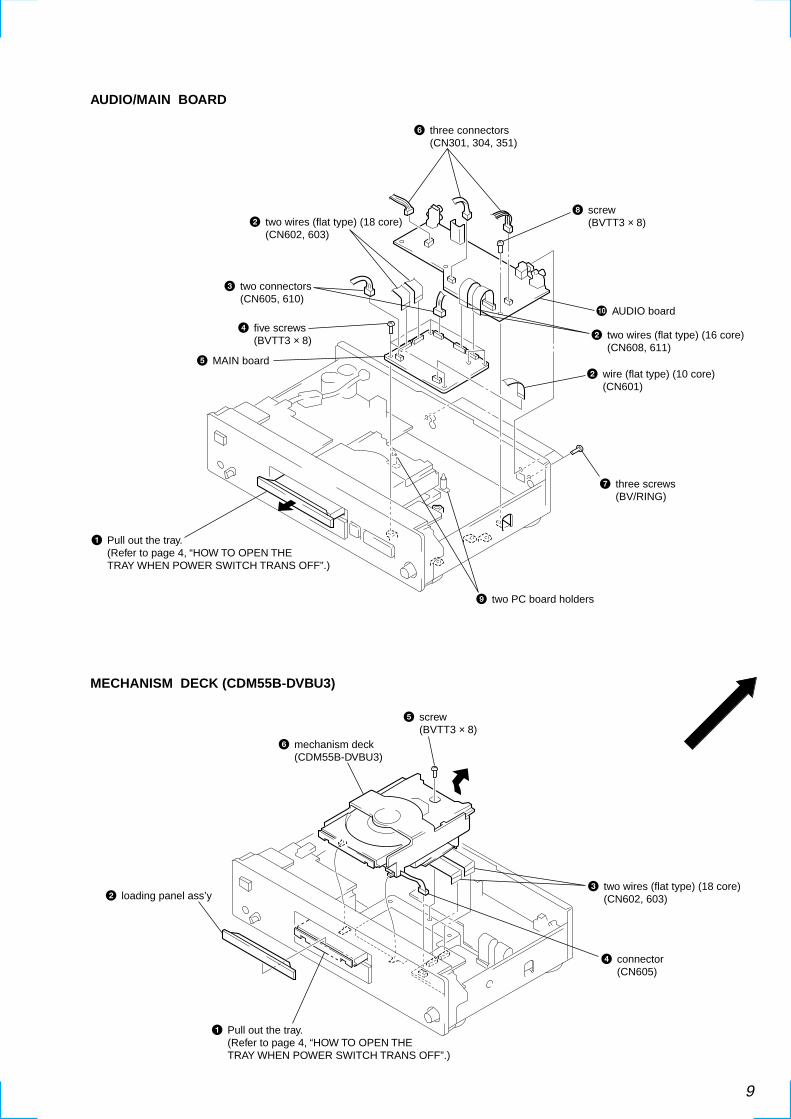
TRAY
1 Remove the tray. (Careful of the claw.)
claw
claw

1111
SECTION 4DIAGRAMS
4-1. NOTE FOR PRINTED WIRING BOARDS AND SCHEMATIC DIAGRAMS
Note on Printed Wiring Board:• X : parts extracted from the component side.• Y : parts extracted from the conductor side.• a : Through hole.• b : Pattern from the side which enables seeing.(The other layers' patterns are not indicated.)
Caution:Pattern face side: Parts on the pattern face side seen from(Conductor Side) the pattern face are indicated.Parts face side: Parts on the parts face side seen from(Component Side) the parts face are indicated.
• Main board is multi-layer printed board.However, the patterns of intermediate-layer have not been in-cluded in the diagram.
• Indication of transistor
C
B
These are omitted.
E
Q
Note on Schematic Diagram:• All capacitors are in µF unless otherwise noted. pF: µµF
50 WV or less are not indicated except for electrolyticsand tantalums.
• All resistors are in Ω and 1/4 W or less unless otherwise
specified.• f : internal component.• 5 : fusible resistor.• C : panel designation.
• U : B+ Line.• V : B– Line.• Voltages and waveforms are dc with respect to ground
under no-signal conditions.no mark : STOP
• Voltages are taken with a VOM (Input impedance 10 MΩ).Voltage variations may be noted due to normal produc-tion tolerances.
• Waveforms are taken with a oscilloscope.Voltage variations may be noted due to normal produc-tion tolerances.
• Circled numbers refer to waveforms.• Signal path.J : SACDc : CDI : DIGITAL OUT
• Circuit Boards Location
TRANSFORMER board POWER board
TK board
AUDIO board
MAIN boardDISPLAY board
LOADING board
HP board
AC SW board
Note: The components identified by mark 0 or dotted linewith mark 0 are critical for safety.Replace only with part number specified.
1212
SCD-XB940
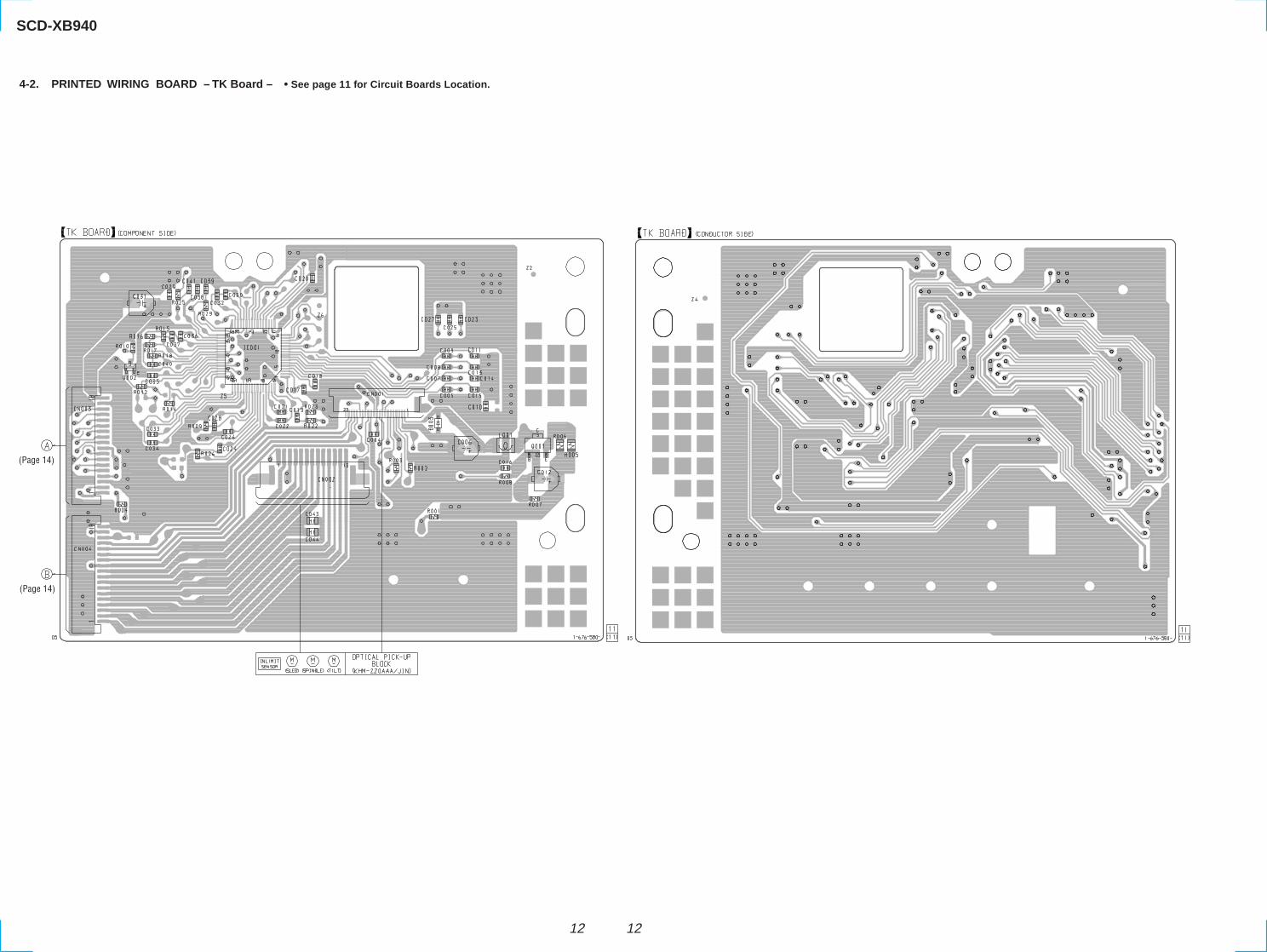
4-2. PRINTED WIRING BOARD – TK Board – • See page 11 for Circuit Boards Location.
(Page 14)
(Page 14)
1313
SCD-XB940
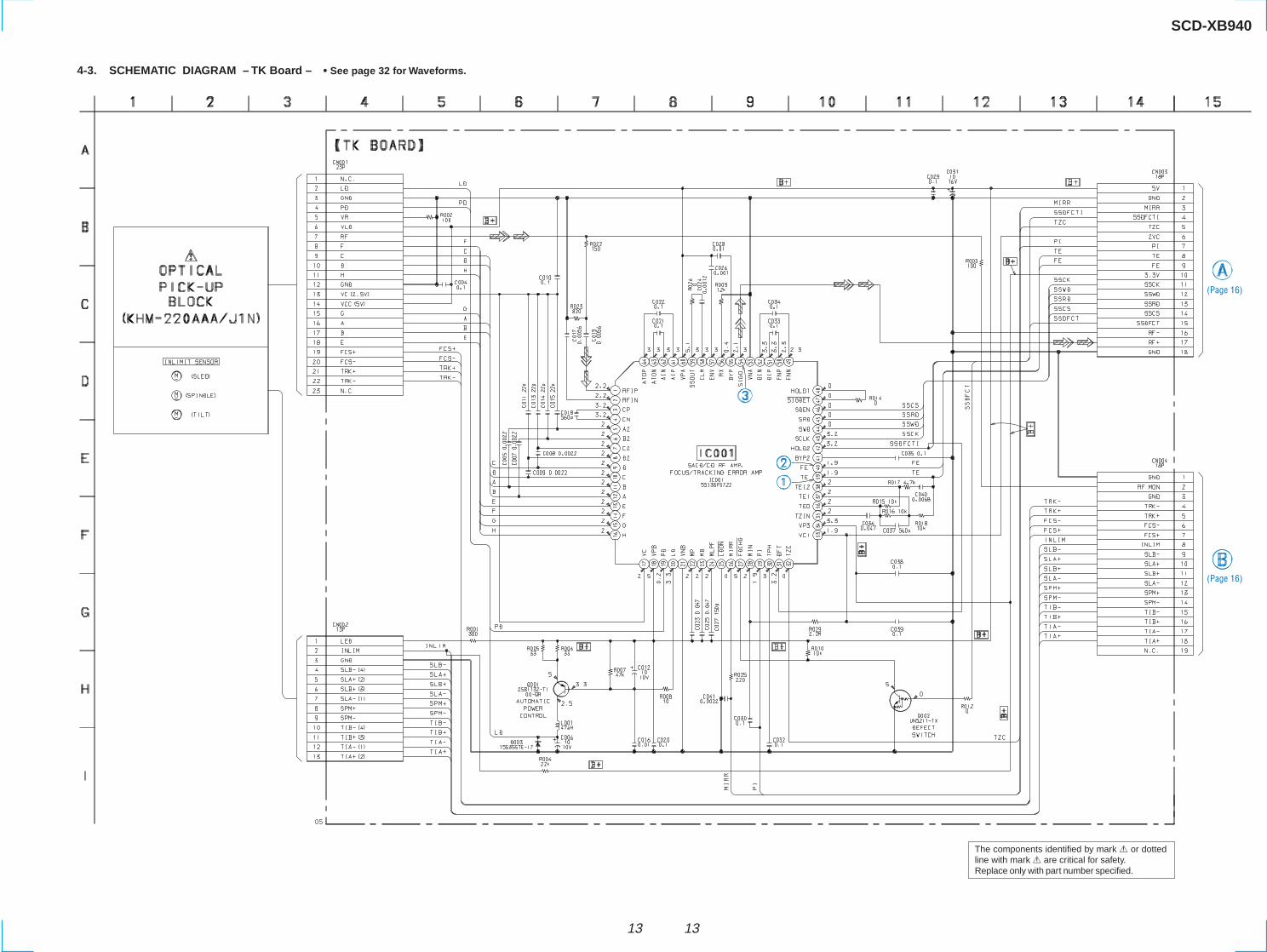
4-3. SCHEMATIC DIAGRAM – TK Board – • See page 32 for Waveforms.
The components identified by mark 0 or dottedline with mark 0 are critical for safety.Replace only with part number specified.
(Page 16)
(Page 16)
1414
SCD-XB940
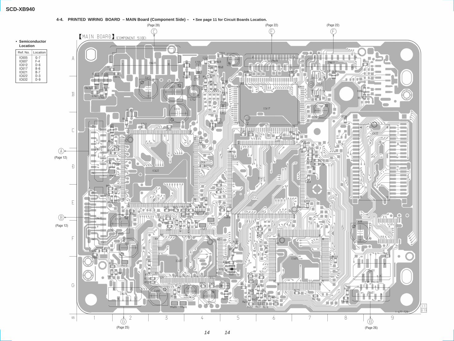
4-4. PRINTED WIRING BOARD – MAIN Board (Component Side) – • See page 11 for Circuit Boards Location.
• SemiconductorLocation
Ref. No. Location
IC605 G-7IC607 F-4IC612 D-6IC617 B-6IC621 B-7IC622 D-3IC632 D-9
(Page 12)
(Page 12)
(Page 28)
(Page 25) (Page 26)
(Page 22) (Page 22)

1515
SCD-XB940
4-5. PRINTED WIRING BOARD – MAIN Board (Conductor Side) – • See page 11 for Circuit Boards Location.
• SemiconductorLocation
Ref. No. Location
D600 G-3D604 G-3D605 E-3D606 G-2D607 E-2D608 G-2D609 G-3D610 G-3D612 G-9
IC600 G-6IC606 G-6IC609 D-9IC610 F-4IC613 G-4IC614 F-2IC615 G-2IC616 C-2IC618 C-4IC619 E-1IC620 A-4IC623 C-6IC624 A-7IC625 B-6IC627 B-4IC628 D-3IC629 B-4IC630 B-4
Q601 G-3Q602 E-4Q603 F-4

1616
SCD-XB940
4-6. SCHEMATIC DIAGRAM – MAIN Board (1/6) – • See page 32 for Waveforms.
(Page 29)
(Page 13)
(Page 13)
(Page 27)
(Page 19) (Page 20)
(Page 21)
(Page20)
(Page 20)
(Page 17)
(Page 18)

1717
SCD-XB940
4-7. SCHEMATIC DIAGRAM – MAIN Board (2/6) –
(Page 16)
(Page 20)
(Page 21)
(Page 18)
(Page 21)

1818
SCD-XB940
4-8. SCHEMATIC DIAGRAM – MAIN Board (3/6) – • See page 32 for Waveforms. • See page 34 for IC Block Diagram.
(Page 16)
(Page 17)
(Page 19)
(Page 20)
(Page 21)
(Page 23)
(Page 23)
(Page 25)

1919
SCD-XB940
4-9. SCHEMATIC DIAGRAM – MAIN Board (4/6) – • See page 32 for Waveform.
(Page 16)
(Page 18)
(Page 20)

2020
SCD-XB940
4-10. SCHEMATIC DIAGRAM – MAIN Board (5/6) –
(Page 16)
(Page 19)
(Page 17) (Page 16) (Page 16)
(Page 18)
(Page 21)

2121
SCD-XB9404-11. SCHEMATIC DIAGRAM – MAIN Board (6/6) – • See page 32 for Waveforms. • See page 34 for IC Block Diagram.
(Page 17)
(Page 16)
(Page 17)
(Page 20)
(Page 18)

2222
SCD-XB9404-12. PRINTED WIRING BOARD – AUDIO Board – • See page 11 for Circuit Boards Location.
• SemiconductorLocation
Ref. No. Location
D302 C-2D303 F-2D321 E-13
IC301 E-17IC302 E-11IC303 F-11IC304 C-11IC305 B-11IC306 C-19IC307 E-6IC308 A-6IC309 C-18IC331 C-3IC352 A-16IC401 F-15IC402 D-9IC403 D-7IC501 C-14IC502 B-9IC503 B-7
Q301 F-1Q302 F-2Q303 F-3Q351 A-19Q403 C-2Q503 C-2
(Page 28)
(Page 24)
(Page 14) (Page 14)
(Page28)

2323
SCD-XB940
4-13. SCHEMATIC DIAGRAM – AUDIO Board – • See page 32 for Waveforms. • See page 34 for IC Block Diagrams.
The components identified by mark 0 or dottedline with mark 0 are critical for safety.Replace only with part number specified.
(Page 29)
(Page 18)
(Page 18)
(Page 29)
(Page 24)

2424
SCD-XB940
4-14. PRINTED WIRING BOARD – HP Board – • See page 11 for Circuit Boards Location. 4-15. SCHEMATIC DIAGRAM – HP Board –
(Page 22)
(Page 23)

2525
SCD-XB940
4-16. PRINTED WIRING BOARD – LOADING Board – • See page 11 for Circuit Boards Location. 4-17. SCHEMATIC DIAGRAM – LOADING Board –
05
(OPEN/CLOSE)
(Page 14)
(Page 18)

2626
SCD-XB940
4-18. PRINTED WIRING BOARD – DISPLAY Board – • See page 11 for Circuit Boards Location.
• SemiconductorLocation
Ref. No. Location
D201 A-3
IC201 C-9IC202 C-6IC203 B-4IC271 A-4
Q201 C-7Q202 C-7Q203 C-7
(Page 14) (Page 28)

2727
SCD-XB940
4-19. SCHEMATIC DIAGRAM – DISPLAY Board – • See page 32 for Waveforms.
(Page 29)
(Page 16)
2828
SCD-XB940
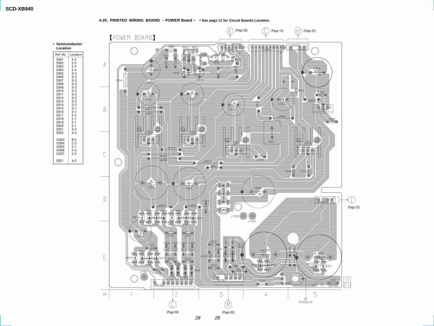
4-20. PRINTED WIRING BOARD – POWER Board – • See page 11 for Circuit Boards Location.
• SemiconductorLocation
Ref. No. Location
D901 E-5D902 E-5D903 E-4D904 E-4D905 D-3D906 D-3D907 D-3D908 D-3D909 D-2D910 D-2D911 D-2D912 D-2D913 D-2D914 D-2D915 D-1D916 D-1D917 E-2D918 E-1D919 E-1D920 E-1D921 A-2D922 A-3
IC903 B-5IC904 C-3IC905 C-1IC906 C-5IC907 C-2
Q921 A-2
(Page 30) (Page 30)
(Page 22)
(Page 26) (Page 14) (Page 22)

2929
SCD-XB9404-21. SCHEMATIC DIAGRAM – POWER Board –
The components identified by mark 0 or dottedline with mark 0 are critical for safety.Replace only with part number specified.
(Page 27)
(Page 16)
(Page 23)
(Page 23)
(Page 31)
(Page 31)

3030
SCD-XB940
4-22. PRINTED WIRING BOARDS – AC SW/TRANSFORMER Boards – • See page 11 for Circuit Boards Location.
TOTRANSFORMER
BOARD
TOAC SWBOARD
(Page 28)(Page 28)
3131
SCD-XB940
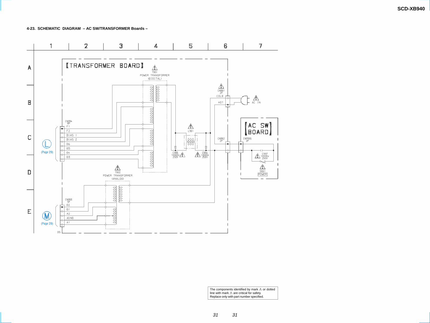
4-23. SCHEMATIC DIAGRAM – AC SW/TRANSFORMER Boards –
The components identified by mark 0 or dottedline with mark 0 are critical for safety.Replace only with part number specified.
(Page 29)
(Page 29)

3232
• Waveforms– TK Board –
1 IC001 el (TE) (CD PLAY)
2 IC001 r; (FE) (CD PLAY)
3 IC001 tf (SIGO) (CD PLAY)
Approx.100 mVp-p
Approx.60 mVp-p
Approx.1.4 Vp-p
2 IC607 yk (ADC1) (CD PLAY)
3 IC607 yl (ADC0) (CD PLAY)
– MAIN Board –
1 IC607 <z/, (X2/CLKIN)
4 IC605 tf (X0)
5 IC617 5 (SDCK)
3.5 Vp-p
27 MHz
Approx.60 mVp-p
Approx.100 mVp-p
3.5 Vp-p
12.5 MHz
4 Vp-p
296 ns
7 IC617 rh (BCKA)
8 IC621 8 (X2Q)
6 IC617 rs (BCKD)
9 IC621 qa (2CK)
q; IC623 1
2.1 Vp-p
88.5 ns
3.8 Vp-p
177 ns
3.7 Vp-p
354 ns
3.1 Vp-p
177 ns
3.4 Vp-p
354 ns
qa IC617 qf (MCKI)IC622 <zxc (SCKI), IC623 8
qs IC622 ql (RFIN2) (CD PLAY)
qd IC622 oa (SDCK)
2 IC301 rf (LVCKO2),IC309 1 (CLK)
3 IC301 rl (BCKI)
– AUDIO Board –
1 IC301 qs (XOUT)
4 IC301 t; (LRCKI)
5 IC301 ta (SBCKI)
6 IC309 5 (Q)
qf IC622 <z/, (BCLK)
qg IC622 <z/. (LRCK)
2.9 Vp-p
29.5 ns
Approx.1.4 Vp-p
3.8 Vp-p
296 ns
3.4 Vp-p
354 ns
3.5 Vp-p
22.7 µs
1.7 Vp-p
45 MHz
3.2 Vp-p
88.5 ns
3.4 Vp-p
354 ns
3.5 Vp-p
22.7 µs
3.4 Vp-p
354 ns
4.4 Vp-p
177 ns

33
2 IC203 ea (EXTAL)
– DISPLAY Board –
1 IC201 tk (OSCO)
4.1 Vp-p
484 ns
3.8 Vp-p
8 MHz

34
• IC Block Diagrams– MAIN Board –
IC621 SN74LV74APWR
IC628 MSM54V16258BSL-40TS-K
14
1 2 3 4 5 6 7
13 12 11 10 9 8VCC
GND
CKCLR
CKCLR
QPR
Q
QPR
Q
D
D
NC
A8 A7 A6 A5 A4 VSS
A0 A1 A2 A3 VCC
VCC
DQ0
DQ1
DQ2
DQ3
VCC
DQ4
DQ5
DQ6
DQ7
WE
RAS
NC
28 2627 232425
18 2019 222121 43 65 87 109
VSS
DQ15
DQ14
DQ13
DQ12
VSS
DQ11
DQ10
DQ9
DQ8
4344 4142 3940 3738 3536 31
I/OSE
LECT
OR
OUTPUTBUFFER
INPUTBUFFER
OUTPUTBUFFER
INPUTBUFFER
SENSEAMPLIFIER
COLUMNDECODERS
MEMORYCELLS
WORDDRIVERS
ROWDECODERS
COLUMNADDRESSBUFFERS
LCAS
30
UCAS
29
OE
I/OCONTROLLER
I/OCONTROLLER
15 16 1711 – 14
NC
34 – 32
ROWADDRESSBUFFERS
INTERNALADDRESSCOUNTER
REFRESHCONTROL
CLOCK
TIMINGGENERATOR

35
– AUDIO Board –
IC309 TC7W74F
IC401, 501 CXA8042AS
6CL
R7
PR
8
VCC
5
Q
RS Q
3
Q
2
D
4
GND
1
CK
QDC
123456789
10
11
121314
28272625242322212019
1817
1615
SWITCHINGCIRCUIT
CONSTANTCURRENTCIRCUIT
REFERENCEVOLTAGECIRCUIT
CONTROLCIRCUIT
I01+ IN2–IN2+NCIN1+IN1–NCC4C3GND2VEE2
VEE1C6
C5CIREF
I02–NC
I01–I02+
NCVCC2
C2C1
VCC1
VREF
VCNTGND1RIREF

36
(1) COVER SECTION
SECTION 5EXPLODED VIEWS
The components identified bymark 0 or dotted line with mark0 are critical for safety.Replace only with part numberspecified.
• Items marked “*” are not stocked since theyare seldom required for routine service. Somedelay should be anticipated when orderingthese items.
• The mechanical parts with no reference num-ber in the exploded views are not supplied.
• Hardware (# mark) list and accessories andpacking materials are given in the last of theelectrical parts list.
NOTE:• -XX and -X mean standardized parts, so they
may have some difference from the originalone.
• Color Indication of Appearance PartsExample:KNOB, BALANCE (WHITE) . . . (RED)
↑ ↑Parts Color Cabinet's Color
7
7
3
7
8
4
56
4
5
1
2
#1
#1
Front panel section
Ref. No. Part No. Description Remark Ref. No. Part No. Description Remark
1 X-4952-805-1 PANEL ASSY, LOADING (BLACK)1 X-4952-806-1 PANEL ASSY, LOADING (SILVER)2 3-704-515-31 SCREW (BV/RING)3 4-210-291-01 SCREW (CASE3 TP2) (AEP: BLACK)3 4-210-291-11 SCREW (CASE3 TP2) (AEP: SILVER)
3 4-210-082-01 SCREW (CASE) (UK)4 4-970-123-11 FOOT (F50180S) (BLACK)4 4-970-123-31 FOOT (F50180S) (SILVER)
5 4-972-889-01 CUSHION6 1-792-598-11 WIRE (FLAT TYPE) (10 CORE)7 4-227-843-01 SCREW (TP), FLAT HEAD (AEP: BLACK)7 4-227-843-11 SCREW (TP), FLAT HEAD (AEP: SILVER)7 4-210-082-01 SCREW (CASE) (UK)
* 8 4-997-138-02 COVER (4095269) (BLACK)* 8 4-997-138-42 COVER (4095269) (SILVER)

37
(2) FRONT PANEL SECTION
not supplied
#3
not supplied
supplied withJ601
supplied with RV601
#2
58
58
58
66
64
65
51
52
53
54
55
63
62
61
56
57
58
59
5860
54
Ref. No. Part No. Description Remark Ref. No. Part No. Description Remark
51 4-227-839-01 PANEL, FRONT (BLACK)51 4-227-839-11 PANEL, FRONT (SILVER)52 4-227-834-01 KNOB (AMS) (BLACK)52 4-227-834-11 KNOB (AMS) (SILVER)53 3-354-931-01 KNOB (DIA. 10) (BLACK)
53 3-354-931-41 KNOB (DIA. 10) (SILVER)54 3-354-981-01 SPRING (SUS), RING55 4-942-568-41 EMBLEM (NO. 5), SONY (for BLACK)55 4-942-568-61 EMBLEM (NO. 5), SONY (for SILVER)56 4-227-832-01 BASE (L), PANEL (BLACK)
56 4-227-832-11 BASE (L), PANEL (SILVER)57 4-998-790-31 KNOB, POWER (BLACK)57 4-998-790-41 KNOB, POWER (SILVER)
58 4-951-620-01 SCREW (2.6X8), +BVTP59 1-677-735-11 AC SW BOARD60 1-677-734-11 HP BOARD61 4-227-841-01 EMBLEM (SACD) (for BLACK)61 4-227-841-11 EMBLEM (SACD) (for SILVER)
62 4-227-184-01 BASE (M), PANEL (BLACK)62 4-227-184-11 BASE (M), PANEL (SILVER)63 4-227-835-01 PLATE, INDICATION64 4-227-183-01 BASE (R), PANEL (BLACK)64 4-227-183-11 BASE (R), PANEL (SILVER)
65 4-227-833-01 BUTTON (PLAY) (A. H. X. x) (BLACK)65 4-227-833-11 BUTTON (PLAY) (A. H. X. x) (SILVER)66 A-4725-091-A DISPLAY BOARD, COMPLETE
38
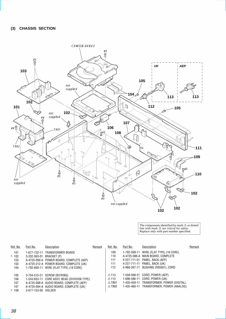
(3) CHASSIS SECTION
#5
#5
CDM55B-DVBU3
notsupplied
notsupplied
notsupplied
#4
#4
T902
T901
#5
#5
#5
#5
#5
not supplied
#5
UK AEP
113 113
112 105
105
104
107
108106
111
109
110
102
102102
101102
103
102
Ref. No. Part No. Description Remark Ref. No. Part No. Description Remark
101 1-677-732-11 TRANSFORMER BOARD* 102 3-332-563-01 BRACKET (P)
103 A-4725-090-A POWER BOARD, COMPLETE (AEP)103 A-4725-212-A POWER BOARD, COMPLETE (UK)104 1-792-600-11 WIRE (FLAT TYPE) (18 CORE)
105 3-704-515-21 SCREW (BV/RING)106 1-543-653-11 CORE ASSY, BEAD (DIVISION TYPE)107 A-4725-088-A AUDIO BOARD, COMPLETE (AEP)107 A-4725-094-A AUDIO BOARD, COMPLETE (UK)
* 108 3-677-153-00 HOLDER
109 1-792-599-11 WIRE (FLAT TYPE) (16 CORE)110 A-4725-086-A MAIN BOARD, COMPLETE111 4-227-711-01 PANEL, BACK (AEP)111 4-227-711-11 PANEL, BACK (UK)112 4-966-267-11 BUSHING (FBS001), CORD
0113 1-558-568-21 CORD, POWER (AEP)0113 1-696-586-11 CORD, POWER (UK)0T901 1-435-459-11 TRANSFORMER, POWER (DIGITAL)0T902 1-435-460-11 TRANSFORMER, POWER (ANALOG)
The components identified by mark 0 or dottedline with mark 0 are critical for safety.Replace only with part number specified.
39
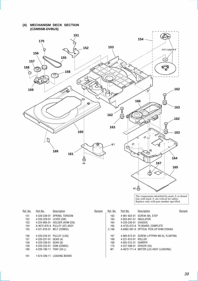
(4) MECHANISM DECK SECTION(CDM55B-DVBU3)
not supplied
170
M1
153
151154
152
155156
157
168158
159
160
169161
162
162
162
163
166
163
163
164
165167
#6
#6
Ref. No. Part No. Description Remark Ref. No. Part No. Description Remark
151 4-220-239-01 SPRING, TORSION152 4-220-229-01 LEVER (SW)153 4-224-895-01 HOLDER (KHM-220)154 A-4672-876-A PULLEY (AT) ASSY155 4-221-816-01 BELT (CDM55)
156 4-220-234-01 PULLEY (LDG)157 4-220-237-01 GEAR (A)158 4-220-238-01 GEAR (B)159 4-220-233-01 CAM (CDM55)160 4-226-180-11 TRAY (55-L)
161 1-674-336-11 LOADING BOARD
162 4-981-923-01 SCREW (M), STEP163 3-053-847-01 INSULATOR164 4-220-230-01 CHASSIS165 A-4725-072-A TK BOARD, COMPLETE
0166 A-6062-397-A OPTICAL PICK-UP KHM-220AAA
167 4-985-672-01 SCREW (+PTPWH M2.6), FLOATING168 4-221-815-01 ROLLER169 4-925-315-31 DAMPER170 4-227-598-01 SPACER (55)M1 A-4672-771-A MOTOR (LD) ASSY (LOADING)
The components identified by mark 0 or dottedline with mark 0 are critical for safety.Replace only with part number specified.
40
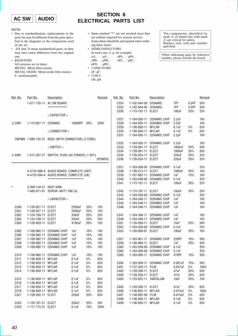
SECTION 6ELECTRICAL PARTS LISTAC SW AUDIO
Ref. No. Part No. Description Remark Ref. No. Part No. Description Remark
1-677-735-11 AC SW BOARD************
< CAPACITOR >
0C997 1-113-927-11 CERAMIC 10000PF 20% 250V
< CONNECTOR >
CNP995 1-690-122-31 REED (WITH CONNECTOR) (2 CORE)
< SWITCH >
0S991 1-572-267-21 SWITCH, PUSH (AC POWER) (1 KEY)(POWER)
**************************************************************
A-4725-088-A AUDIO BOARD, COMPLETE (AEP)A-4725-094-A AUDIO BOARD, COMPLETE (UK)
**********************
* 3-309-144-21 HEAT SINK7-685-871-01 SCREW +BVTT 3X6 (S)
< CAPACITOR >
C300 1-126-927-11 ELECT 2200uF 20% 10VC301 1-126-927-11 ELECT 2200uF 20% 10VC302 1-124-700-11 ELECT 330uF 20% 25VC303 1-124-700-11 ELECT 330uF 20% 25VC304 1-126-929-11 ELECT 4700uF 20% 10V
C305 1-109-982-11 CERAMIC CHIP 1uF 10% 10VC306 1-109-982-11 CERAMIC CHIP 1uF 10% 10VC307 1-109-982-11 CERAMIC CHIP 1uF 10% 10VC308 1-109-982-11 CERAMIC CHIP 1uF 10% 10VC309 1-109-982-11 CERAMIC CHIP 1uF 10% 10V
C310 1-109-982-11 CERAMIC CHIP 1uF 10% 10VC311 1-136-850-11 MYLAR 0.1uF 5% 63VC312 1-136-850-11 MYLAR 0.1uF 5% 63VC313 1-136-850-11 MYLAR 0.1uF 5% 63VC314 1-136-850-11 MYLAR 0.1uF 5% 63V
C315 1-136-850-11 MYLAR 0.1uF 5% 63VC316 1-136-850-11 MYLAR 0.1uF 5% 63VC317 1-136-850-11 MYLAR 0.1uF 5% 63VC318 1-136-850-11 MYLAR 0.1uF 5% 63VC321 1-128-202-11 ELECT 220uF 20% 63V
C322 1-125-781-21 ELECT 220uF 20% 35VC323 1-117-775-31 ELECT 0.1uF 10% 250V
NOTE:• Due to standardization, replacements in the
parts list may be different from the parts speci-fied in the diagrams or the components usedon the set.
• -XX and -X mean standardized parts, so theymay have some difference from the originalone.
• RESISTORSAll resistors are in ohms.METAL: Metal-film resistor.METAL OXIDE: Metal oxide-film resistor.F: nonflammable
• Items marked “*” are not stocked since theyare seldom required for routine service.Some delay should be anticipated when order-ing these items.
• SEMICONDUCTORSIn each case, u: µ, for example:uA. . : µA. . uPA. . : µPA. .uPB. . : µPB. . uPC. . : µPC. .uPD. . : µPD. .
• CAPACITORSuF: µF
• COILSuH: µH
The components identified bymark 0 or dotted line with mark0 are critical for safety.Replace only with part numberspecified.
When indicating parts by referencenumber, please include the board.
C324 1-102-944-00 CERAMIC 7PF 0.5PF 50VC325 1-102-944-00 CERAMIC 7PF 0.5PF 50VC326 1-115-197-11 ELECT 100uF 20% 25V
C327 1-164-505-11 CERAMIC CHIP 2.2uF 16VC328 1-164-505-11 CERAMIC CHIP 2.2uF 16VC329 1-136-850-11 MYLAR 0.1uF 5% 63VC330 1-136-850-11 MYLAR 0.1uF 5% 63VC331 1-164-505-11 CERAMIC CHIP 2.2uF 16V
C332 1-164-505-11 CERAMIC CHIP 2.2uF 16VC333 1-128-091-11 ELECT 1000uF 20% 50VC334 1-128-091-11 ELECT 1000uF 20% 50VC335 1-126-024-11 ELECT 220uF 20% 25VC336 1-126-024-11 ELECT 220uF 20% 25V
C337 1-163-038-00 CERAMIC CHIP 0.1uF 25VC338 1-126-013-11 ELECT 1000uF 20% 16VC339 1-107-682-11 CERAMIC CHIP 1uF 10% 16VC340 1-163-038-00 CERAMIC CHIP 0.1uF 25VC341 1-115-197-11 ELECT 100uF 20% 25V
C342 1-115-197-11 ELECT 100uF 20% 25VC343 1-163-038-00 CERAMIC CHIP 0.1uF 25VC344 1-164-346-11 CERAMIC CHIP 1uF 16VC345 1-164-346-11 CERAMIC CHIP 1uF 16VC346 1-164-346-11 CERAMIC CHIP 1uF 16V
C347 1-164-346-11 CERAMIC CHIP 1uF 16VC348 1-164-346-11 CERAMIC CHIP 1uF 16VC351 1-126-059-11 ELECT 10uF 20% 50VC352 1-163-038-00 CERAMIC CHIP 0.1uF 25VC353 1-126-009-81 ELECT 100uF 20% 16V
C357 1-163-001-11 CERAMIC CHIP 220PF 10% 50VC358 1-126-960-11 ELECT 1uF 20% 50VC363 1-163-038-00 CERAMIC CHIP 0.1uF 25VC364 1-163-038-00 CERAMIC CHIP 0.1uF 25VC392 1-163-005-11 CERAMIC CHIP 470PF 10% 50V
C393 1-163-009-11 CERAMIC CHIP 0.001uF 10% 50VC401 1-137-420-11 FILM 0.047uF 5% 100VC402 1-128-200-11 ELECT 47uF 20% 63VC403 1-128-200-11 ELECT 47uF 20% 63VC404 1-125-822-11 TANTALUM 10uF 20% 10V
C405 1-128-200-11 ELECT 47uF 20% 63VC406 1-136-802-11 MYLAR 0.015uF 5% 100VC407 1-130-892-00 FILM 0.015uF 5% 63VC408 1-136-850-11 MYLAR 0.1uF 5% 63VC409 1-136-850-11 MYLAR 0.1uF 5% 63V

41
Ref. No. Part No. Description Remark Ref. No. Part No. Description Remark
AUDIO
C410 1-130-892-00 FILM 0.015uF 3% 100VC412 1-130-339-11 FILM 0.0056uF 3% 100VC413 1-130-339-11 FILM 0.0056uF 3% 100VC414 1-136-252-00 FILM 0.0015uF 3% 100VC415 1-136-252-00 FILM 0.0015uF 3% 100V
C416 1-136-816-11 FILM 0.0022uF 5% 100VC417 1-136-257-00 FILM 0.0039uF 3% 100VC420 1-128-201-11 ELECT 100uF 20% 63VC421 1-128-201-11 ELECT 100uF 20% 63VC422 1-137-506-11 ELECT 0.47uF 10% 63V
C423 1-136-808-11 FILM 100PF 5% 100VC424 1-163-021-11 CERAMIC CHIP 0.01uF 10% 50VC451 1-163-239-11 CERAMIC CHIP 33PF 5% 50VC452 1-164-505-11 CERAMIC CHIP 2.2 uF 16VC453 1-125-859-21 FILM 0.001uF 5% 50V
C501 1-137-420-11 FILM 0.047uF 5% 100VC502 1-128-200-11 ELECT 47uF 20% 63VC503 1-128-200-11 ELECT 47uF 20% 63VC504 1-125-822-11 TANTALUM 10uF 20% 10VC505 1-128-200-11 ELECT 47uF 20% 63V
C506 1-136-802-11 MYLAR 0.015uF 5% 100VC507 1-130-892-00 FILM 0.015uF 5% 63VC508 1-136-850-11 MYLAR 0.1uF 5% 63VC509 1-136-850-11 MYLAR 0.1uF 5% 63VC510 1-130-892-00 FILM 0.015uF 3% 100V
C512 1-130-339-11 FILM 0.0056uF 3% 100VC513 1-130-339-11 FILM 0.0056uF 3% 100VC514 1-136-252-00 FILM 0.0015uF 3% 100VC515 1-136-252-00 FILM 0.0015uF 3% 100VC516 1-136-816-11 FILM 0.0022uF 5% 100V
C517 1-136-257-00 FILM 0.0039uF 3% 100VC520 1-128-201-11 ELECT 100uF 20% 63VC521 1-128-201-11 ELECT 100uF 20% 63VC522 1-137-506-11 ELECT 0.47uF 10% 63VC523 1-136-808-11 CERAMIC CHIP 100PF 5% 100V
C524 1-163-021-11 CERAMIC CHIP 0.01uF 10% 50VC551 1-163-239-11 CERAMIC CHIP 33PF 5% 50VC552 1-164-505-11 CERAMIC CHIP 2.2uF 16VC553 1-125-859-21 FILM 0.001uF 5% 50V
< CONNECTOR >
* CN301 1-564-506-11 PLUG, CONNECTOR 3PCN302 1-770-646-11 CONNECTOR, FFC/FPC 16PCN303 1-770-646-11 CONNECTOR, FFC/FPC 16P
* CN304 1-564-506-11 PLUG, CONNECTOR 3PCN351 1-506-468-11 PIN, CONNECTOR 3P
< DIODE >
D302 8-719-016-74 DIODE 1SS352-TPH3D303 8-719-977-13 DIODE DTZ-TT11-6.8CD321 8-719-210-39 DIODE EC10QS04-TE12L5
< GROUND TERMINAL >
EB301 1-537-770-21 TERMINAL BOARD, GROUND
< IC >
IC301 8-759-653-12 IC CXD9556QIC302 8-759-231-53 IC M5F7805L
IC303 8-759-231-53 IC M5F7805LIC304 8-759-604-86 IC M5F7807LIC305 8-759-604-90 IC M5F7907L
IC306 8-759-445-59 IC BA033TIC307 8-759-231-58 IC M5F7812LIC308 8-759-245-86 IC M5F7912LIC309 8-759-180-84 IC TC7W74F (TE12R)IC331 8-759-711-85 IC NJM4580E-D-TE2
IC352 8-749-921-12 IC GP1F32T (DIGITAL OUT CD OPTICAL)IC401 8-759-371-51 IC CXA8042ASIC402 8-759-443-33 IC OPA2132PAIC403 8-759-686-08 IC OPA2604AU/2K5IC501 8-759-371-51 IC CXA8042AS
IC502 8-759-443-33 IC OPA2132PAIC503 8-759-686-08 IC OPA2604AU/2K5
< JACK >
J301 1-774-727-11 JACK, PIN 2P (ANALOG OUT)J351 1-770-905-21 JACK, PIN 1P (DIGITAL OUT CD COAXIAL)
< SHORT >
JW304 1-216-295-00 SHORT 0JW305 1-216-295-00 SHORT 0
< RESISTOR/NOISE FILTER/FERRITE BEAD >
L302 1-216-042-00 METAL CHIP 510 5% 1/10WL303 1-216-295-00 SHORT 0L304 1-216-042-00 METAL CHIP 510 5% 1/10WL306 1-216-061-00 METAL CHIP 3.3K 5% 1/10WL307 1-216-049-11 METAL CHIP 1K 5% 1/10W
L308 1-216-057-00 METAL CHIP 2.2K 5% 1/10WL309 1-424-122-11 FILTER, NOISEL310 1-424-122-11 FILTER, NOISEL311 1-424-122-11 FILTER, NOISEL312 1-424-122-11 FILTER, NOISE
L321 1-424-122-11 FILTER, NOISEL322 1-424-153-11 FILTER, NOISEL351 1-216-295-00 SHORT 0L352 1-414-234-22 FERRITE BEADL353 1-414-234-22 FERRITE BEAD
L354 1-414-234-22 FERRITE BEADL401 1-424-122-11 FILTER, NOISEL402 1-424-122-11 FILTER, NOISEL501 1-424-122-11 FILTER, NOISEL502 1-424-122-11 FILTER, NOISE
< TRANSISTOR >
Q301 8-729-027-38 TRANSISTOR DTA144EKA-T146Q302 8-729-900-53 TRANSISTOR DTC114EKA-T146Q303 8-729-027-38 TRANSISTOR DTA144EKA-T146Q351 8-729-120-28 TRANSISTOR 2SC1623-T1-L5L6Q403 8-729-141-74 TRANSISTOR 2SC3624A-T2L15L16
Q503 8-729-141-74 TRANSISTOR 2SC3624A-T2L15L16
< RESISTOR >
R301 1-216-033-00 METAL CHIP 220 5% 1/10W0R302 1-212-857-00 FUSIBLE 10 5% 1/4W F
The components identified by mark 0 or dottedline with mark 0 are critical for safety.Replace only with part number specified.

42
Ref. No. Part No. Description Remark Ref. No. Part No. Description Remark
AUDIO DISPLAY
R303 1-216-097-00 RES-CHIP 100K 5% 1/10WR304 1-216-097-00 RES-CHIP 100K 5% 1/10WR305 1-216-105-00 RES-CHIP 220K 5% 1/10W
R306 1-216-033-00 METAL CHIP 220 5% 1/10WR307 1-216-081-00 METAL CHIP 22K 5% 1/10WR308 1-216-045-00 RES-CHIP 680 5% 1/10WR309 1-216-105-00 RES-CHIP 220K 5% 1/10WR310 1-216-025-00 RES-CHIP 100 5% 1/10W
R311 1-216-025-00 RES-CHIP 100 5% 1/10WR312 1-216-295-00 SHORT 0R321 1-216-061-00 METAL CHIP 3.3K 5% 1/10WR331 1-216-033-00 METAL CHIP 220 5% 1/10WR332 1-216-033-00 METAL CHIP 220 5% 1/10W
R353 1-216-055-00 METAL CHIP 1.8K 5% 1/10WR354 1-216-063-00 RES-CHIP 3.9K 5% 1/10WR355 1-216-057-00 METAL CHIP 2.2K 5% 1/10WR356 1-216-033-00 METAL CHIP 220 5% 1/10WR357 1-216-021-00 METAL CHIP 68 5% 1/10W
R358 1-216-097-00 RES-CHIP 100K 5% 1/10WR361 1-216-295-00 SHORT 0R371 1-216-053-00 METAL CHIP 1.5K 5% 1/10WR373 1-216-041-00 METAL CHIP 470 5% 1/10WR374 1-216-045-00 METAL CHIP 680 5% 1/10W
R375 1-216-057-00 METAL CHIP 2.2K 5% 1/10WR376 1-216-055-00 METAL CHIP 1.8K 5% 1/10WR392 1-216-041-00 METAL CHIP 470 5% 1/10WR398 1-216-049-11 RES-CHIP 1K 5% 1/10WR399 1-216-049-11 RES-CHIP 1K 5% 1/10W
R401 1-216-023-00 METAL CHIP 82 5% 1/10WR402 1-216-017-91 METAL CHIP 47 5% 1/10WR403 1-216-017-91 METAL CHIP 47 5% 1/10WR404 1-216-023-00 METAL CHIP 82 5% 1/10WR405 1-216-001-00 METAL CHIP 10 5% 1/10W
R406 1-216-001-00 METAL CHIP 10 5% 1/10WR407 1-259-971-11 CARBON MELF 10 2% 1/8WR408 1-259-971-11 CARBON MELF 10 2% 1/8WR409 1-259-989-11 CARBON MELF 330 2% 1/8WR410 1-259-989-11 CARBON MELF 330 2% 1/8W
R411 1-259-977-11 CARBON MELF 33 2% 1/8WR412 1-259-977-11 CARBON MELF 33 2% 1/8WR415 1-259-997-11 CARBON MELF 1.5K 2% 1/8WR416 1-259-997-11 CARBON MELF 1.5K 2% 1/8WR417 1-259-926-11 CARBON MELF 2K 2% 1/8W
R418 1-259-926-11 CARBON MELF 2K 2% 1/8WR419 1-259-995-11 CARBON MELF 1K 2% 1/8WR420 1-259-995-11 CARBON MELF 1K 2% 1/8WR423 1-260-026-11 CARBON MELF 330K 2% 1/8WR424 1-259-975-11 CARBON MELF 22 2% 1/8W
R426 1-259-971-11 CARBON MELF 10 2% 1/8WR427 1-216-105-00 RES-CHIP 220K 5% 1/10WR431 1-259-992-11 CARBON MELF 560 2% 1/8WR432 1-216-057-00 METAL CHIP 2.2K 5% 1/10WR451 1-216-085-00 METAL CHIP 33K 5% 1/10W
R452 1-216-104-00 METAL CHIP 200K 5% 1/10WR453 1-216-107-00 METAL CHIP 270K 5% 1/10WR454 1-216-119-00 METAL CHIP 820K 5% 1/10WR455 1-216-019-00 METAL CHIP 56 5% 1/10WR463 1-216-057-00 METAL CHIP 2.2K 5% 1/10W
R501 1-216-023-00 METAL CHIP 82 5% 1/10WR502 1-216-017-91 METAL CHIP 47 5% 1/10WR503 1-216-017-91 METAL CHIP 47 5% 1/10WR504 1-216-023-00 METAL CHIP 82 5% 1/10WR505 1-216-001-00 METAL CHIP 10 5% 1/10W
R506 1-216-001-00 METAL CHIP 10 5% 1/10WR507 1-259-971-11 CARBON MELF 10 2% 1/8WR508 1-259-971-11 CARBON MELF 10 2% 1/8WR509 1-259-989-11 CARBON MELF 330 2% 1/8WR510 1-259-989-11 CARBON MELF 330 2% 1/8W
R511 1-259-977-11 CARBON MELF 33 2% 1/8WR512 1-259-977-11 CARBON MELF 33 2% 1/8WR515 1-259-997-11 CARBON MELF 1.5K 2% 1/8WR516 1-259-997-11 CARBON MELF 1.5K 2% 1/8WR517 1-259-926-11 CARBON MELF 2K 2% 1/8W
R518 1-259-926-11 CARBON MELF 2K 2% 1/8WR519 1-259-995-11 CARBON MELF 1K 2% 1/8WR520 1-259-995-11 CARBON MELF 1K 2% 1/8WR523 1-260-026-11 CARBON MELF 330K 2% 1/8WR524 1-259-975-11 CARBON MELF 22 2% 1/8W
R526 1-259-971-11 CARBON MELF 10 2% 1/8WR527 1-216-105-00 RES-CHIP 220K 5% 1/10WR531 1-259-992-11 CARBON MELF 560 2% 1/8WR532 1-216-057-00 METAL CHIP 2.2K 5% 1/10WR551 1-216-085-00 METAL CHIP 33K 5% 1/10W
R552 1-216-104-00 METAL CHIP 200K 5% 1/10WR553 1-216-107-00 METAL CHIP 270K 5% 1/10WR554 1-216-119-00 METAL CHIP 820K 5% 1/10WR555 1-216-019-00 METAL CHIP 56 5% 1/10WR563 1-216-057-00 METAL CHIP 2.2K 5% 1/10W
R1001 1-216-295-00 SHORT 0R1002 1-216-001-00 METAL CHIP 10 5% 1/10WR1003 1-216-295-00 SHORT 0
< RELAY >
RY301 1-755-295-11 RELAY
< VIBRATOR >
X321 1-760-955-11 VIBRATOR, CRYSTAL (45MHz)**************************************************************
A-4725-091-A DISPLAY BOARD, COMPLETE************************
3-350-124-11 CUSHION (EJECT)
< CAPACITOR >
C201 1-163-038-00 CERAMIC CHIP 0.1uF 25VC202 1-163-117-00 CERAMIC CHIP 100PF 5% 50VC203 1-163-117-00 CERAMIC CHIP 100PF 5% 50VC204 1-163-038-00 CERAMIC CHIP 0.1uF 25VC205 1-163-104-00 CERAMIC CHIP 30PF 5% 50V
C206 1-163-033-00 CERAMIC CHIP 0.022uF 50VC207 1-163-038-00 CERAMIC CHIP 0.1uF 25VC208 1-126-177-11 ELECT 100uF 20% 10VC209 1-165-319-11 CERAMIC CHIP 0.1uF 50VC210 1-163-038-00 CERAMIC CHIP 0.1uF 25V

43
Ref. No. Part No. Description Remark Ref. No. Part No. Description Remark
C211 1-126-154-11 ELECT 47uF 20% 6.3VC212 1-163-038-00 CERAMIC CHIP 0.1uF 25VC213 1-163-009-11 CERAMIC CHIP 0.001uF 10% 50VC214 1-163-038-00 CERAMIC CHIP 0.1uF 25VC215 1-163-038-00 CERAMIC CHIP 0.1uF 25V
C216 1-163-117-00 CERAMIC CHIP 100PF 5% 50VC217 1-163-117-00 CERAMIC CHIP 100PF 5% 50VC218 1-163-117-00 CERAMIC CHIP 100PF 5% 50VC219 1-163-117-00 CERAMIC CHIP 100PF 5% 50VC220 1-163-117-00 CERAMIC CHIP 100PF 5% 50V
C221 1-163-117-00 CERAMIC CHIP 100PF 5% 50VC222 1-163-117-00 CERAMIC CHIP 100PF 5% 50VC223 1-163-117-00 CERAMIC CHIP 100PF 5% 50VC224 1-163-117-00 CERAMIC CHIP 100PF 5% 50VC225 1-163-038-00 CERAMIC CHIP 0.1uF 25V
C226 1-163-005-11 CERAMIC CHIP 470PF 10% 50VC227 1-163-005-11 CERAMIC CHIP 470PF 10% 50VC271 1-163-038-00 CERAMIC CHIP 0.1uF 25VC272 1-163-021-11 CERAMIC CHIP 0.01uF 10% 50V
< CONNECTOR >
* CN202 1-770-641-11 CONNECTOR, FFC/FPC 10P
< DIODE >
D201 8-719-016-74 DIODE 1SS352-TPH3
< FLUORESCENT INDICATOR TUBE >
FL201 1-517-966-11 TUBE, FLUORESCENT INDICATOR
< IC >
IC201 8-759-337-52 IC LC75721EIC202 8-759-459-85 IC NJL63H400A ( )IC203 8-752-915-71 IC CXP84120-087QIC271 8-759-342-61 IC PST575DMT
< TRANSISTOR >
Q201 8-729-900-53 TRANSISTOR DTC114EKA-T146Q202 8-729-900-53 TRANSISTOR DTC114EKA-T146Q203 8-729-900-53 TRANSISTOR DTC114EKA-T146
< RESISTOR >
R204 1-216-097-00 RES-CHIP 100K 5% 1/10WR213 1-216-025-00 RES-CHIP 100 5% 1/10WR215 1-216-025-00 RES-CHIP 100 5% 1/10WR217 1-216-025-00 RES-CHIP 100 5% 1/10WR219 1-216-073-00 METAL CHIP 10K 5% 1/10W
R220 1-216-097-00 RES-CHIP 100K 5% 1/10WR221 1-216-025-00 RES-CHIP 100 5% 1/10WR222 1-216-073-00 METAL CHIP 10K 5% 1/10WR223 1-216-073-00 METAL CHIP 10K 5% 1/10WR224 1-216-073-00 METAL CHIP 10K 5% 1/10W
R225 1-216-097-00 RES-CHIP 100K 5% 1/10WR227 1-216-073-00 METAL CHIP 10K 5% 1/10WR230 1-216-073-00 METAL CHIP 10K 5% 1/10WR231 1-216-073-00 METAL CHIP 10K 5% 1/10WR232 1-216-073-00 METAL CHIP 10K 5% 1/10W
R233 1-216-073-00 METAL CHIP 10K 5% 1/10W
R234 1-216-073-00 METAL CHIP 10K 5% 1/10WR235 1-216-073-00 METAL CHIP 10K 5% 1/10WR236 1-216-073-00 METAL CHIP 10K 5% 1/10WR237 1-216-025-00 RES-CHIP 100 5% 1/10W
R238 1-216-025-00 RES-CHIP 100 5% 1/10WR239 1-216-025-00 RES-CHIP 100 5% 1/10WR240 1-216-025-00 RES-CHIP 100 5% 1/10WR241 1-216-025-00 RES-CHIP 100 5% 1/10WR242 1-216-073-00 METAL CHIP 10K 5% 1/10W
R251 1-216-069-00 METAL CHIP 6.8K 5% 1/10WR252 1-216-045-00 METAL CHIP 680 5% 1/10WR253 1-216-049-11 RES-CHIP 1K 5% 1/10WR254 1-216-053-00 METAL CHIP 1.5K 5% 1/10WR257 1-216-069-00 METAL CHIP 6.8K 5% 1/10W
R260 1-216-061-00 METAL CHIP 3.3K 5% 1/10WR261 1-216-073-00 METAL CHIP 10K 5% 1/10WR262 1-216-073-00 METAL CHIP 10K 5% 1/10WR264 1-216-077-00 RES-CHIP 15K 5% 1/10WR266 1-216-001-00 METAL CHIP 10 5% 1/10W
R271 1-216-097-00 RES-CHIP 100K 5% 1/10W
< COMPOSITION CIRCUIT BLOCK >
RB201 1-234-520-11 CIRCUIT BLOCK, COMPOSITION 10KRB202 1-234-521-11 CIRCUIT BLOCK, COMPOSITION 15KRB203 1-234-521-11 CIRCUIT BLOCK, COMPOSITION 15K
< SWITCH >
S201 1-475-543-11 ENCODER, ROTARY(l AMS L PUSH ENTER)
S251 1-762-875-21 SWITCH, KEYBOARD (A)S252 1-762-875-21 SWITCH, KEYBOARD (G)S253 1-762-875-21 SWITCH, KEYBOARD (X)S254 1-762-875-21 SWITCH, KEYBOARD (x)
< VIBRATOR >
X201 1-781-472-21 VIBRATOR, CERAMIC (8MHz)**************************************************************
1-677-734-11 HP BOARD*********
< CAPACITOR >
C601 1-163-038-00 CERAMIC CHIP 0.1uF 25VC602 1-163-038-00 CERAMIC CHIP 0.1uF 25VC603 1-163-038-00 CERAMIC CHIP 0.1uF 25V
< JACK >
J601 1-770-307-11 JACK (LARGE TYPE) (PHONES)
< NOISE FILTER/SHORT/COIL >
L601 1-424-122-11 FILTER, NOISEL602 1-424-122-11 FILTER, NOISEL603 1-424-122-11 FILTER, NOISEL604 1-424-122-11 FILTER, NOISEL605 1-216-295-00 SHORT 0
L606 1-216-295-00 SHORT 0L607 1-216-295-00 SHORT 0L608 1-414-180-11 INDUCTOR 3.3uH
DISPLAY HP

44
Ref. No. Part No. Description Remark Ref. No. Part No. Description Remark
HP LOADING MAIN
L609 1-414-180-11 INDUCTOR 3.3uHL610 1-414-180-11 INDUCTOR 3.3uH
< VARIABLE RESISTOR >
RV601 1-227-185-11 RES, VAR, CARBON 1K/1K (PHONE LEVEL)**************************************************************
1-674-336-11 LOADING BOARD**************
< CONNECTOR >
* CN151 1-568-943-11 PIN, CONNECTOR 5P
< SWITCH >
S1 1-771-799-11 SWITCH, LEVER (SLIDE) (OPEN/CLOSE)**************************************************************
A-4725-086-A MAIN BOARD, COMPLETE*********************
< CAPACITOR >
C606 1-162-970-11 CERAMIC CHIP 0.01uF 10% 25VC607 1-126-246-11 ELECT CHIP 220uF 20% 4VC608 1-126-246-11 ELECT CHIP 220uF 20% 4VC609 1-115-156-11 CERAMIC CHIP 1uF 10VC612 1-126-246-11 ELECT CHIP 220uF 20% 4V
C614 1-162-970-11 CERAMIC CHIP 0.01uF 10% 25VC616 1-126-206-11 ELECT CHIP 100uF 20% 6.3VC617 1-162-970-11 CERAMIC CHIP 0.01uF 10% 25VC618 1-162-970-11 CERAMIC CHIP 0.01uF 10% 25VC619 1-115-467-11 CERAMIC CHIP 0.22uF 10% 10V
C620 1-107-826-11 CERAMIC CHIP 0.1uF 10% 16VC621 1-162-970-11 CERAMIC CHIP 0.01uF 10% 25VC624 1-162-970-11 CERAMIC CHIP 0.01uF 10% 25VC625 1-162-970-11 CERAMIC CHIP 0.01uF 10% 25VC626 1-115-156-11 CERAMIC CHIP 1uF 10V
C627 1-162-970-11 CERAMIC CHIP 0.01uF 10% 25VC628 1-125-822-11 TANTALUM 10uF 20% 10VC629 1-162-970-11 CERAMIC CHIP 0.01uF 10% 25VC630 1-125-822-11 TANTALUM 10uF 20% 10VC631 1-162-970-11 CERAMIC CHIP 0.01uF 10% 25V
C632 1-162-970-11 CERAMIC CHIP 0.01uF 10% 25VC633 1-162-970-11 CERAMIC CHIP 0.01uF 10% 25VC634 1-162-970-11 CERAMIC CHIP 0.01uF 10% 25VC635 1-162-968-11 CERAMIC CHIP 0.0047uF 10% 50VC636 1-162-968-11 CERAMIC CHIP 0.0047uF 10% 50V
C637 1-162-968-11 CERAMIC CHIP 0.0047uF 10% 50VC638 1-162-968-11 CERAMIC CHIP 0.0047uF 10% 50VC639 1-107-826-11 CERAMIC CHIP 0.1uF 10% 16VC640 1-125-822-11 TANTALUM 10uF 20% 10VC641 1-162-970-11 CERAMIC CHIP 0.01uF 10% 25V
C642 1-165-176-11 CERAMIC CHIP 0.047uF 10% 16VC643 1-165-176-11 CERAMIC CHIP 0.047uF 10% 16VC644 1-107-826-11 CERAMIC CHIP 0.1uF 10% 16VC645 1-107-826-11 CERAMIC CHIP 0.1uF 10% 16VC646 1-162-970-11 CERAMIC CHIP 0.01uF 10% 25V
C647 1-162-970-11 CERAMIC CHIP 0.01uF 10% 25VC650 1-107-826-11 CERAMIC CHIP 0.1uF 10% 16V
C651 1-107-826-11 CERAMIC CHIP 0.1uF 10% 16VC652 1-107-826-11 CERAMIC CHIP 0.1uF 10% 16VC653 1-162-970-11 CERAMIC CHIP 0.01uF 10% 25V
C654 1-162-970-11 CERAMIC CHIP 0.01uF 10% 25VC655 1-162-970-11 CERAMIC CHIP 0.01uF 10% 25VC656 1-162-970-11 CERAMIC CHIP 0.01uF 10% 25VC657 1-162-970-11 CERAMIC CHIP 0.01uF 10% 25VC658 1-162-970-11 CERAMIC CHIP 0.01uF 10% 25V
C659 1-125-822-11 TANTALUM 10uF 20% 10VC660 1-164-677-11 CERAMIC CHIP 0.033uF 10% 16VC661 1-164-677-11 CERAMIC CHIP 0.033uF 10% 16VC662 1-110-563-11 CERAMIC CHIP 0.068uF 10% 16VC663 1-110-563-11 CERAMIC CHIP 0.068uF 10% 16V
C664 1-162-923-11 CERAMIC CHIP 47PF 5% 50VC665 1-162-923-11 CERAMIC CHIP 47PF 5% 50VC666 1-162-927-11 CERAMIC CHIP 100PF 5% 50VC667 1-162-927-11 CERAMIC CHIP 100PF 5% 50VC668 1-164-230-11 CERAMIC CHIP 220PF 5% 50V
C669 1-164-230-11 CERAMIC CHIP 220PF 5% 50VC670 1-107-826-11 CERAMIC CHIP 0.1uF 10% 16VC671 1-107-826-11 CERAMIC CHIP 0.1uF 10% 16VC672 1-115-467-11 CERAMIC CHIP 0.22uF 10% 10VC673 1-124-779-00 ELECT CHIP 10uF 20% 16V
C674 1-124-778-00 ELECT CHIP 22uF 20% 6.3VC675 1-115-467-11 CERAMIC CHIP 0.22uF 10% 10VC676 1-115-467-11 CERAMIC CHIP 0.22uF 10% 10VC677 1-165-176-11 CERAMIC CHIP 0.047uF 10% 16VC680 1-117-681-11 ELECT CHIP 100uF 20% 16V
C681 1-117-681-11 ELECT CHIP 100uF 20% 16VC682 1-107-826-11 CERAMIC CHIP 0.1uF 10% 16VC683 1-165-176-11 CERAMIC CHIP 0.047uF 10% 16VC684 1-107-826-11 CERAMIC CHIP 0.1uF 10% 16VC685 1-162-967-11 CERAMIC CHIP 0.0033uF 10% 50V
C686 1-162-967-11 CERAMIC CHIP 0.0033uF 10% 50VC687 1-162-970-11 CERAMIC CHIP 0.01uF 10% 25VC688 1-162-970-11 CERAMIC CHIP 0.01uF 10% 25VC689 1-162-970-11 CERAMIC CHIP 0.01uF 10% 25VC690 1-162-970-11 CERAMIC CHIP 0.01uF 10% 25V
C691 1-162-970-11 CERAMIC CHIP 0.01uF 10% 25VC692 1-162-970-11 CERAMIC CHIP 0.01uF 10% 25VC693 1-125-822-11 TANTALUM 10uF 20% 10VC694 1-162-970-11 CERAMIC CHIP 0.01uF 10% 25VC695 1-162-970-11 CERAMIC CHIP 0.01uF 10% 25V
C696 1-162-927-11 CERAMIC CHIP 100PF 5% 50VC697 1-162-970-11 CERAMIC CHIP 0.01uF 10% 25VC698 1-162-970-11 CERAMIC CHIP 0.01uF 10% 25VC700 1-107-548-11 ELECT CHIP 22uF 20% 16VC701 1-162-970-11 CERAMIC CHIP 0.01uF 10% 25V
C702 1-162-970-11 CERAMIC CHIP 0.01uF 10% 25VC703 1-162-970-11 CERAMIC CHIP 0.01uF 10% 25VC704 1-124-779-00 ELECT CHIP 10uF 20% 16VC705 1-110-563-11 CERAMIC CHIP 0.068uF 10% 16VC706 1-107-826-11 CERAMIC CHIP 0.1uF 10% 16V
C707 1-165-176-11 CERAMIC CHIP 0.047uF 10% 16VC708 1-164-677-11 CERAMIC CHIP 0.033uF 10% 16VC709 1-162-970-11 CERAMIC CHIP 0.01uF 10% 25VC710 1-125-822-11 TANTALUM 10uF 20% 10VC711 1-162-927-11 CERAMIC CHIP 100PF 5% 50V

45
Ref. No. Part No. Description Remark Ref. No. Part No. Description Remark
MAIN
C712 1-107-826-11 CERAMIC CHIP 0.1uF 10% 16VC713 1-107-826-11 CERAMIC CHIP 0.1uF 10% 16VC714 1-125-822-11 TANTALUM 10uF 20% 10VC715 1-107-826-11 CERAMIC CHIP 0.1uF 10% 16VC716 1-107-826-11 CERAMIC CHIP 0.1uF 10% 16V
C717 1-107-826-11 CERAMIC CHIP 0.1uF 10% 16VC718 1-107-826-11 CERAMIC CHIP 0.1uF 10% 16VC719 1-107-826-11 CERAMIC CHIP 0.1uF 10% 16VC720 1-107-826-11 CERAMIC CHIP 0.1uF 10% 16VC721 1-107-826-11 CERAMIC CHIP 0.1uF 10% 16V
C722 1-107-826-11 CERAMIC CHIP 0.1uF 10% 16VC723 1-107-826-11 CERAMIC CHIP 0.1uF 10% 16VC724 1-107-826-11 CERAMIC CHIP 0.1uF 10% 16VC725 1-107-826-11 CERAMIC CHIP 0.1uF 10% 16VC726 1-107-826-11 CERAMIC CHIP 0.1uF 10% 16V
C727 1-126-206-11 ELECT CHIP 100uF 20% 6.3VC728 1-107-826-11 CERAMIC CHIP 0.1uF 10% 16VC729 1-125-822-11 TANTALUM 10uF 20% 10VC730 1-162-970-11 CERAMIC CHIP 0.01uF 10% 25VC731 1-125-822-11 TANTALUM 10uF 20% 10V
C732 1-162-970-11 CERAMIC CHIP 0.01uF 10% 25VC733 1-107-826-11 CERAMIC CHIP 0.1uF 10% 16VC734 1-125-822-11 TANTALUM 10uF 20% 10VC735 1-125-822-11 TANTALUM 10uF 20% 10VC736 1-162-970-11 CERAMIC CHIP 0.01uF 10% 25V
C737 1-162-970-11 CERAMIC CHIP 0.01uF 10% 25VC738 1-162-970-11 CERAMIC CHIP 0.01uF 10% 25VC739 1-162-945-11 CERAMIC CHIP 22PF 5% 50VC740 1-162-945-11 CERAMIC CHIP 22PF 5% 50VC741 1-162-945-11 CERAMIC CHIP 22PF 5% 50V
C742 1-162-970-11 CERAMIC CHIP 0.01uF 10% 25VC743 1-162-970-11 CERAMIC CHIP 0.01uF 10% 25VC744 1-162-970-11 CERAMIC CHIP 0.01uF 10% 25VC745 1-162-970-11 CERAMIC CHIP 0.01uF 10% 25VC746 1-162-970-11 CERAMIC CHIP 0.01uF 10% 25V
C747 1-125-822-11 TANTALUM 10uF 20% 10VC748 1-125-822-11 TANTALUM 10uF 20% 10VC749 1-162-970-11 CERAMIC CHIP 0.01uF 10% 25VC751 1-162-970-11 CERAMIC CHIP 0.01uF 10% 25VC752 1-124-778-00 ELECT CHIP 22uF 20% 6.3V
C753 1-162-970-11 CERAMIC CHIP 0.01uF 10% 25VC754 1-162-970-11 CERAMIC CHIP 0.01uF 10% 25VC755 1-162-970-11 CERAMIC CHIP 0.01uF 10% 25VC756 1-162-970-11 CERAMIC CHIP 0.01uF 10% 25VC757 1-162-970-11 CERAMIC CHIP 0.01uF 10% 25V
C759 1-162-970-11 CERAMIC CHIP 0.01uF 10% 25VC760 1-162-970-11 CERAMIC CHIP 0.01uF 10% 25VC762 1-164-346-11 CERAMIC CHIP 1uF 16VC763 1-164-346-11 CERAMIC CHIP 1uF 16V
< CONNECTOR >
CN600 1-790-675-11 PIN, CONNECTOR (PC BOARD) 7PCN601 1-784-369-21 CONNECTOR, FFC/FPC 10PCN602 1-793-990-11 CONNECTOR, FFC/FPC 18PCN603 1-793-990-11 CONNECTOR, FFC/FPC 18PCN605 1-790-669-21 PIN, CONNECTOR (PC BOARD) 9P
CN608 1-784-375-21 CONNECTOR, FFC/FPC 16P
CN610 1-794-296-11 PIN, CONNECTOR (PC BOARD) 6PCN611 1-784-375-21 CONNECTOR, FFC/FPC 16P
< DIODE >
D600 8-719-988-61 DIODE 1SS355TE-17D604 8-719-988-61 DIODE 1SS355TE-17D605 8-719-941-86 DIODE DAN202UT106D606 8-719-941-86 DIODE DAN202UT106D607 8-719-988-61 DIODE 1SS355TE-17
D608 8-719-941-09 DIODE DAP202UT106D609 8-719-941-09 DIODE DAP202UT106D610 8-719-988-61 DIODE 1SS355TE-17D612 8-719-988-61 DIODE 1SS355TE-17
< FERRITE BEAD >
FB600 1-500-283-11 FERRITE BEADFB601 1-500-283-11 FERRITE BEADFB604 1-500-283-11 FERRITE BEADFB605 1-500-283-11 FERRITE BEADFB606 1-500-283-11 FERRITE BEAD
FB607 1-500-283-11 FERRITE BEADFB608 1-500-283-11 FERRITE BEADFB609 1-500-283-11 FERRITE BEADFB610 1-500-283-11 FERRITE BEADFB611 1-500-283-11 FERRITE BEAD
FB612 1-500-283-11 FERRITE BEADFB613 1-500-283-11 FERRITE BEADFB615 1-500-283-11 FERRITE BEADFB616 1-500-283-11 FERRITE BEADFB617 1-500-283-11 FERRITE BEAD
FB618 1-500-283-11 FERRITE BEADFB619 1-500-283-11 FERRITE BEADFB620 1-500-283-11 FERRITE BEADFB621 1-500-283-11 FERRITE BEADFB636 1-500-283-11 FERRITE BEAD
< EMI FILTER >
FL600 1-234-177-21 FILTER, CHIP EMIFL601 1-234-177-21 FILTER, CHIP EMIFL603 1-234-177-21 FILTER, CHIP EMIFL604 1-234-177-21 FILTER, CHIP EMIFL605 1-234-177-21 FILTER, CHIP EMI
FL606 1-233-893-21 FILTER, CHIP EMIFL607 1-234-177-21 FILTER, CHIP EMIFL608 1-234-177-21 FILTER, CHIP EMIFL610 1-234-177-21 FILTER, CHIP EMIFL611 1-234-177-21 FILTER, CHIP EMI
FL612 1-233-893-21 FILTER, CHIP EMIFL613 1-234-177-21 FILTER, CHIP EMIFL614 1-234-177-21 FILTER, CHIP EMIFL616 1-234-177-21 FILTER, CHIP EMIFL617 1-239-400-11 FILTER, CHIP EMI
FL618 1-234-177-21 FILTER, CHIP EMIFL619 1-239-400-11 FILTER, CHIP EMIFL620 1-234-177-21 FILTER, CHIP EMIFL621 1-234-177-21 FILTER, CHIP EMIFL622 1-234-177-21 FILTER, CHIP EMI
FL623 1-234-177-21 FILTER, CHIP EMI

46
Ref. No. Part No. Description Remark Ref. No. Part No. Description Remark
MAIN
FL624 1-234-177-21 FILTER, CHIP EMIFL625 1-234-177-21 FILTER, CHIP EMIFL626 1-234-177-21 FILTER, CHIP EMIFL627 1-234-177-21 FILTER, CHIP EMI
FL628 1-234-177-21 FILTER, CHIP EMI
< IC >
IC600 8-759-362-00 IC BR9040F-E2IC605 8-759-663-92 IC MB91107PFV-G-BNDIC606 8-759-645-76 IC TC74VHCT32AFTIC607 8-759-598-87 IC CXD8791AQIC609 8-759-573-65 IC IDT71V016S20PHAU-TL
IC610 8-759-337-40 IC NJM2904V (TE2)IC612 8-759-591-83 IC CXD9515QIC613 8-759-338-78 IC BA10324AFV-E2IC614 8-759-522-13 IC BA5981FP-E2IC615 8-759-567-26 IC BA5983FP-E2
IC616 8-759-548-96 IC SN74LV02APWRIC617 8-752-400-60 IC CXD2751QIC618 8-759-449-58 IC LM7131BCM5XIC619 8-759-486-55 IC NJM2370U33-TE2IC620 8-752-356-45 IC CXD2301Q
IC621 8-759-549-23 IC SN74LV74APWRIC622 8-759-567-27 IC CXD8784RIC623 8-759-549-25 IC SN74LVU04APWRIC624 8-759-585-52 IC SN74AHC1GU04DBVRIC625 8-759-676-10 IC MSM51V17805B-60TS-K
IC627 8-759-585-51 IC SN74AHC1G32DBVRIC628 8-759-597-78 IC MSM54V16258BSL-40TSKIC629 8-759-585-51 IC SN74AHC1G32DBVRIC630 8-759-585-51 IC SN74AHC1G32DBVRIC632 8-759-679-85 IC MR27V402D-16MPZ060
< COIL >
L602 1-410-369-11 INDUCTOR CHIP 1uHL603 1-410-369-11 INDUCTOR CHIP 1uHL604 1-410-369-11 INDUCTOR CHIP 1uHL605 1-410-369-11 INDUCTOR CHIP 1uH
< TRANSISTOR >
Q601 8-729-015-74 TRANSISTOR UN5111-TXQ602 8-729-230-63 TRANSISTOR 2SD1819A-QRS-TXQ603 8-729-230-63 TRANSISTOR 2SD1819A-QRS-TX
< RESISTOR >
R601 1-216-833-11 RES-CHIP 10K 5% 1/16WR603 1-216-821-11 METAL CHIP 1K 5% 1/16WR604 1-216-829-11 METAL CHIP 4.7K 5% 1/16WR605 1-216-809-11 METAL CHIP 100 5% 1/16WR606 1-216-809-11 METAL CHIP 100 5% 1/16W
R607 1-216-809-11 METAL CHIP 100 5% 1/16WR608 1-216-809-11 METAL CHIP 100 5% 1/16WR609 1-216-864-11 METAL CHIP 0 5% 1/16WR610 1-216-809-11 METAL CHIP 100 5% 1/16WR611 1-216-833-11 RES-CHIP 10K 5% 1/16W
R612 1-216-833-11 RES-CHIP 10K 5% 1/16WR613 1-216-825-11 METAL CHIP 2.2K 5% 1/16WR614 1-216-833-11 RES-CHIP 10K 5% 1/16WR615 1-216-833-11 RES-CHIP 10K 5% 1/16W
R616 1-216-833-11 RES-CHIP 10K 5% 1/16W
R617 1-216-833-11 RES-CHIP 10K 5% 1/16WR618 1-216-813-11 METAL CHIP 220 5% 1/16WR619 1-216-833-11 RES-CHIP 10K 5% 1/16WR620 1-216-813-11 METAL CHIP 220 5% 1/16WR621 1-216-813-11 METAL CHIP 220 5% 1/16W
R622 1-216-813-11 METAL CHIP 220 5% 1/16WR624 1-216-813-11 METAL CHIP 220 5% 1/16WR625 1-216-833-11 RES-CHIP 10K 5% 1/16WR626 1-216-813-11 METAL CHIP 220 5% 1/16WR627 1-216-833-11 RES-CHIP 10K 5% 1/16W
R628 1-216-813-11 METAL CHIP 220 5% 1/16WR629 1-216-833-11 RES-CHIP 10K 5% 1/16WR631 1-216-813-11 METAL CHIP 220 5% 1/16WR632 1-216-833-11 RES-CHIP 10K 5% 1/16WR634 1-216-813-11 METAL CHIP 220 5% 1/16W
R636 1-216-833-11 RES-CHIP 10K 5% 1/16WR638 1-216-813-11 METAL CHIP 220 5% 1/16WR639 1-216-833-11 RES-CHIP 10K 5% 1/16WR640 1-216-809-11 METAL CHIP 100 5% 1/16WR641 1-216-809-11 METAL CHIP 100 5% 1/16W
R643 1-216-809-11 METAL CHIP 100 5% 1/16WR644 1-216-805-11 METAL CHIP 47 5% 1/16WR645 1-216-809-11 METAL CHIP 100 5% 1/16WR646 1-216-833-11 RES-CHIP 10K 5% 1/16WR647 1-216-833-11 RES-CHIP 10K 5% 1/16W
R648 1-216-809-11 METAL CHIP 100 5% 1/16WR649 1-216-833-11 RES-CHIP 10K 5% 1/16WR650 1-216-809-11 METAL CHIP 100 5% 1/16WR651 1-216-813-11 METAL CHIP 220 5% 1/16WR652 1-216-809-11 METAL CHIP 100 5% 1/16W
R653 1-216-809-11 METAL CHIP 100 5% 1/16WR655 1-216-833-11 RES-CHIP 10K 5% 1/16WR656 1-216-845-11 METAL CHIP 100K 5% 1/16WR657 1-216-821-11 METAL CHIP 1K 5% 1/16WR674 1-216-833-11 RES-CHIP 10K 5% 1/16W
R675 1-216-841-11 METAL CHIP 47K 5% 1/16WR680 1-216-833-11 RES-CHIP 10K 5% 1/16WR681 1-216-864-11 METAL CHIP 0 5% 1/16WR683 1-216-864-11 METAL CHIP 0 5% 1/16WR684 1-216-845-11 METAL CHIP 100K 5% 1/16W
R686 1-216-833-11 RES-CHIP 10K 5% 1/16WR687 1-216-845-11 METAL CHIP 100K 5% 1/16WR689 1-216-845-11 METAL CHIP 100K 5% 1/16WR690 1-216-801-11 METAL CHIP 22 5% 1/16WR691 1-216-833-11 RES-CHIP 10K 5% 1/16W
R692 1-216-801-11 METAL CHIP 22 5% 1/16WR694 1-216-833-11 RES-CHIP 10K 5% 1/16WR695 1-216-801-11 METAL CHIP 22 5% 1/16WR696 1-216-833-11 RES-CHIP 10K 5% 1/16WR698 1-216-801-11 METAL CHIP 22 5% 1/16W
R699 1-216-833-11 RES-CHIP 10K 5% 1/16WR700 1-216-801-11 METAL CHIP 22 5% 1/16WR701 1-216-833-11 RES-CHIP 10K 5% 1/16WR702 1-216-864-11 METAL CHIP 0 5% 1/16WR703 1-216-805-11 METAL CHIP 47 5% 1/16W
R704 1-216-833-11 RES-CHIP 10K 5% 1/16W

47
Ref. No. Part No. Description Remark Ref. No. Part No. Description Remark
R706 1-216-833-11 RES-CHIP 10K 5% 1/16WR707 1-216-821-11 METAL CHIP 1K 5% 1/16WR708 1-216-821-11 METAL CHIP 1K 5% 1/16WR709 1-216-821-11 METAL CHIP 1K 5% 1/16W
R711 1-216-821-11 METAL CHIP 1K 5% 1/16WR712 1-216-833-11 RES-CHIP 10K 5% 1/16WR713 1-216-833-11 RES-CHIP 10K 5% 1/16WR719 1-216-821-11 METAL CHIP 1K 5% 1/16WR720 1-216-817-11 METAL CHIP 470 5% 1/16W
R721 1-216-817-11 METAL CHIP 470 5% 1/16WR722 1-216-817-11 METAL CHIP 470 5% 1/16WR723 1-216-817-11 METAL CHIP 470 5% 1/16WR724 1-216-864-11 METAL CHIP 0 5% 1/16WR725 1-216-844-11 METAL CHIP 82K 5% 1/16W
R726 1-216-844-11 METAL CHIP 82K 5% 1/16WR727 1-216-844-11 METAL CHIP 82K 5% 1/16WR728 1-216-844-11 METAL CHIP 82K 5% 1/16WR729 1-216-833-11 RES-CHIP 10K 5% 1/16WR730 1-216-839-11 METAL CHIP 33K 5% 1/16W
R731 1-216-833-11 RES-CHIP 10K 5% 1/16WR733 1-216-815-11 METAL CHIP 330 5% 1/16WR734 1-216-836-11 METAL CHIP 18K 5% 1/16WR735 1-216-834-11 METAL CHIP 12K 5% 1/16WR739 1-216-833-11 RES-CHIP 10K 5% 1/16W
R740 1-216-833-11 RES-CHIP 10K 5% 1/16WR741 1-216-833-11 RES-CHIP 10K 5% 1/16WR742 1-216-833-11 RES-CHIP 10K 5% 1/16WR744 1-216-833-11 RES-CHIP 10K 5% 1/16WR745 1-216-833-11 RES-CHIP 10K 5% 1/16W
R746 1-216-817-11 METAL CHIP 470 5% 1/16WR747 1-216-815-11 METAL CHIP 330 5% 1/16WR748 1-216-809-11 METAL CHIP 100 5% 1/16WR749 1-216-821-11 METAL CHIP 1K 5% 1/16WR750 1-216-833-11 RES-CHIP 10K 5% 1/16W
R751 1-218-889-11 METAL CHIP 56K 0.5% 1/16WR752 1-218-899-11 METAL CHIP 150K 0.5% 1/16WR753 1-218-899-11 METAL CHIP 150K 0.5% 1/16WR754 1-218-889-11 METAL CHIP 56K 0.5% 1/16WR755 1-216-840-11 METAL CHIP 39K 5% 1/16W
R756 1-216-840-11 METAL CHIP 39K 5% 1/16WR757 1-216-835-11 METAL CHIP 15K 5% 1/16WR758 1-216-835-11 METAL CHIP 15K 5% 1/16WR759 1-216-833-11 RES-CHIP 10K 5% 1/16WR760 1-216-841-11 METAL CHIP 47K 5% 1/16W
R761 1-216-841-11 METAL CHIP 47K 5% 1/16WR762 1-216-844-11 METAL CHIP 82K 5% 1/16WR763 1-216-844-11 METAL CHIP 82K 5% 1/16WR764 1-216-841-11 METAL CHIP 47K 5% 1/16WR765 1-216-841-11 METAL CHIP 47K 5% 1/16W
R766 1-216-833-11 RES-CHIP 10K 5% 1/16WR767 1-216-847-11 METAL CHIP 150K 5% 1/16WR768 1-216-847-11 METAL CHIP 150K 5% 1/16WR769 1-216-847-11 METAL CHIP 150K 5% 1/16WR770 1-216-296-00 SHORT 0
R771 1-216-138-00 METAL CHIP 3.3 5% 1/8WR772 1-216-848-11 METAL CHIP 180K 5% 1/16WR773 1-216-848-11 METAL CHIP 180K 5% 1/16WR774 1-216-848-11 METAL CHIP 180K 5% 1/16W
R775 1-216-844-11 METAL CHIP 82K 5% 1/16W
R776 1-216-843-11 METAL CHIP 68K 5% 1/16WR777 1-216-837-11 METAL CHIP 22K 5% 1/16WR778 1-216-837-11 METAL CHIP 22K 5% 1/16WR779 1-216-833-11 RES-CHIP 10K 5% 1/16WR780 1-216-833-11 RES-CHIP 10K 5% 1/16W
R781 1-216-851-11 METAL CHIP 330K 5% 1/16WR782 1-216-830-11 METAL CHIP 5.6K 5% 1/16WR783 1-216-833-11 RES-CHIP 10K 5% 1/16WR784 1-216-833-11 RES-CHIP 10K 5% 1/16WR785 1-216-833-11 RES-CHIP 10K 5% 1/16W
R786 1-216-841-11 METAL CHIP 47K 5% 1/16WR787 1-216-843-11 METAL CHIP 68K 5% 1/16WR788 1-216-843-11 METAL CHIP 68K 5% 1/16WR789 1-216-830-11 METAL CHIP 5.6K 5% 1/16WR790 1-218-897-11 METAL CHIP 120K 0.5% 1/16W
R791 1-216-852-11 METAL CHIP 390K 5% 1/16WR792 1-216-845-11 METAL CHIP 100K 5% 1/16WR793 1-216-840-11 METAL CHIP 39K 5% 1/16WR794 1-216-844-11 METAL CHIP 82K 5% 1/16WR795 1-216-844-11 METAL CHIP 82K 5% 1/16W
R796 1-216-833-11 RES-CHIP 10K 5% 1/16WR797 1-216-833-11 RES-CHIP 10K 5% 1/16WR798 1-216-852-11 METAL CHIP 390K 5% 1/16WR799 1-216-845-11 METAL CHIP 100K 5% 1/16WR800 1-216-836-11 METAL CHIP 18K 5% 1/16W
R801 1-216-833-11 RES-CHIP 10K 5% 1/16WR802 1-216-833-11 RES-CHIP 10K 5% 1/16WR803 1-216-851-11 METAL CHIP 330K 5% 1/16WR804 1-216-849-11 METAL CHIP 220K 5% 1/16WR805 1-216-833-11 RES-CHIP 10K 5% 1/16W
R806 1-218-897-11 METAL CHIP 120K 0.5% 1/16WR807 1-216-833-11 RES-CHIP 10K 5% 1/16WR808 1-218-907-11 METAL CHIP 330K 0.5% 1/16WR810 1-218-907-11 METAL CHIP 330K 0.5% 1/16WR811 1-216-833-11 RES-CHIP 10K 5% 1/16W
R812 1-216-809-11 METAL CHIP 100 5% 1/16WR813 1-216-815-11 METAL CHIP 330 5% 1/16WR814 1-216-815-11 METAL CHIP 330 5% 1/16WR815 1-216-833-11 RES-CHIP 10K 5% 1/16WR818 1-216-805-11 METAL CHIP 47 5% 1/16W
R819 1-216-829-11 METAL CHIP 4.7K 5% 1/16WR820 1-216-845-11 METAL CHIP 100K 5% 1/16WR821 1-216-805-11 METAL CHIP 47 5% 1/16WR822 1-216-809-11 METAL CHIP 100 5% 1/16WR823 1-216-829-11 METAL CHIP 4.7K 5% 1/16W
R824 1-218-871-11 METAL CHIP 10K 0.5% 1/16WR825 1-218-871-11 METAL CHIP 10K 0.5% 1/16WR826 1-216-809-11 METAL CHIP 100 5% 1/16WR827 1-216-838-11 METAL CHIP 27K 5% 1/16WR828 1-216-836-11 METAL CHIP 18K 5% 1/16W
R829 1-216-803-11 METAL CHIP 33 5% 1/16WR830 1-218-875-11 METAL CHIP 15K 0.5% 1/16WR831 1-218-871-11 METAL CHIP 10K 0.5% 1/16WR832 1-218-831-11 METAL CHIP 220 0.5% 1/16WR833 1-216-821-11 METAL CHIP 1K 5% 1/16W
R834 1-216-825-11 METAL CHIP 2.2K 5% 1/16W
MAIN

48
Ref. No. Part No. Description Remark Ref. No. Part No. Description Remark
R835 1-216-838-11 METAL CHIP 27K 5% 1/16WR836 1-216-825-11 METAL CHIP 2.2K 5% 1/16WR838 1-216-809-11 METAL CHIP 100 5% 1/16WR839 1-218-871-11 METAL CHIP 10K 0.5% 1/16W
R840 1-218-871-11 METAL CHIP 10K 0.5% 1/16WR841 1-218-847-11 METAL CHIP 1K 0.5% 1/16WR842 1-218-855-11 METAL CHIP 2.2K 0.5% 1/16WR843 1-218-855-11 METAL CHIP 2.2K 0.5% 1/16WR844 1-218-855-11 METAL CHIP 2.2K 0.5% 1/16W
R845 1-216-833-11 RES-CHIP 10K 5% 1/16WR847 1-216-833-11 RES-CHIP 10K 5% 1/16WR848 1-216-833-11 RES-CHIP 10K 5% 1/16WR849 1-216-801-11 METAL CHIP 22 5% 1/16WR850 1-216-801-11 METAL CHIP 22 5% 1/16W
R851 1-216-801-11 METAL CHIP 22 5% 1/16WR852 1-218-853-11 METAL CHIP 1.8K 0.5% 1/16WR853 1-216-813-11 METAL CHIP 220 5% 1/16WR854 1-216-813-11 METAL CHIP 220 5% 1/16WR855 1-216-805-11 METAL CHIP 47 5% 1/16W
R856 1-216-831-11 METAL CHIP 6.8K 5% 1/16WR857 1-216-849-11 METAL CHIP 220K 5% 1/16WR858 1-216-819-11 METAL CHIP 680 5% 1/16WR859 1-216-819-11 METAL CHIP 680 5% 1/16WR860 1-216-819-11 METAL CHIP 680 5% 1/16W
R861 1-216-833-11 RES-CHIP 10K 5% 1/16WR862 1-216-801-11 METAL CHIP 22 5% 1/16WR863 1-216-801-11 METAL CHIP 22 5% 1/16WR864 1-216-801-11 METAL CHIP 22 5% 1/16WR865 1-216-801-11 METAL CHIP 22 5% 1/16W
R866 1-216-801-11 METAL CHIP 22 5% 1/16WR867 1-216-801-11 METAL CHIP 22 5% 1/16WR868 1-216-801-11 METAL CHIP 22 5% 1/16WR869 1-216-801-11 METAL CHIP 22 5% 1/16WR870 1-216-805-11 METAL CHIP 47 5% 1/16W
R871 1-216-809-11 METAL CHIP 100 5% 1/16WR873 1-216-833-11 RES-CHIP 10K 5% 1/16WR876 1-216-833-11 RES-CHIP 10K 5% 1/16WR878 1-216-821-11 METAL CHIP 1K 5% 1/16WR881 1-216-821-11 METAL CHIP 1K 5% 1/16W
R882 1-216-821-11 METAL CHIP 1K 5% 1/16WR883 1-216-821-11 METAL CHIP 1K 5% 1/16WR885 1-216-833-11 RES-CHIP 10K 5% 1/16WR886 1-216-833-11 RES-CHIP 10K 5% 1/16WR887 1-216-833-11 RES-CHIP 10K 5% 1/16W
R889 1-216-833-11 RES-CHIP 10K 5% 1/16WR890 1-216-833-11 RES-CHIP 10K 5% 1/16WR895 1-216-809-11 METAL CHIP 100 5% 1/16WR897 1-216-833-11 RES-CHIP 10K 5% 1/16WR898 1-216-809-11 METAL CHIP 100 5% 1/16W
R899 1-216-809-11 METAL CHIP 100 5% 1/16WR901 1-216-833-11 RES-CHIP 10K 5% 1/16WR902 1-216-833-11 RES-CHIP 10K 5% 1/16WR903 1-216-833-11 RES-CHIP 10K 5% 1/16WR904 1-216-833-11 RES-CHIP 10K 5% 1/16W
R905 1-216-833-11 RES-CHIP 10K 5% 1/16WR906 1-216-833-11 RES-CHIP 10K 5% 1/16WR908 1-216-803-11 METAL CHIP 33 5% 1/16WR909 1-216-815-11 METAL CHIP 330 5% 1/16W
R910 1-216-803-11 METAL CHIP 33 5% 1/16W
R911 1-216-803-11 METAL CHIP 33 5% 1/16WR912 1-216-833-11 RES-CHIP 10K 5% 1/16WR913 1-216-296-00 SHORT 0R914 1-216-833-11 RES-CHIP 10K 5% 1/16WR916 1-216-864-11 METAL CHIP 0 5% 1/16W
R918 1-216-833-11 RES-CHIP 10K 5% 1/16WR919 1-216-833-11 RES-CHIP 10K 5% 1/16WR920 1-216-805-11 METAL CHIP 47 5% 1/16WR921 1-216-805-11 METAL CHIP 47 5% 1/16W
< COMPOSITION CIRCUIT BLOCK >
* RB601 1-233-270-11 NETWORK, RES (8 GANG) 10K* RB602 1-233-270-11 NETWORK, RES (8 GANG) 10K* RB603 1-233-270-11 NETWORK, RES (8 GANG) 10K
< CHECKER TERMINAL >
TP600 1-535-757-11 CHIP, CHECKERTP602 1-535-757-11 CHIP, CHECKERTP603 1-535-757-11 CHIP, CHECKERTP608 1-535-757-11 CHIP, CHECKERTP609 1-535-757-11 CHIP, CHECKER
TP613 1-535-757-11 CHIP, CHECKER
< VIBRATOR >
X600 1-781-185-21 VIBRATOR, CERAMIC (12.5MHz)X601 1-781-408-11 VIBRATOR, CERAMIC (27MHz)
**************************************************************
A-4725-090-A POWER BOARD, COMPLETE (AEP)A-4725-212-A POWER BOARD, COMPLETE (UK)
***********************
7-685-871-01 SCREW +BVTT 3X6 (S)
< CAPACITOR >
C901 1-110-578-11 ELECT (BLOCK) 3300uF 20% 25VC902 1-110-578-11 ELECT (BLOCK) 3300uF 20% 25VC903 1-126-017-11 ELECT 6800uF 20% 16VC904 1-126-939-11 ELECT 10000uF 20% 16VC905 1-111-235-61 ELECT 10000uF 20% 25V
C906 1-126-065-11 ELECT 330uF 20% 63VC907 1-126-064-11 ELECT 220uF 20% 63VC908 1-136-177-00 MYLAR 1uF 5% 50VC909 1-136-177-00 MYLAR 1uF 5% 50VC913 1-124-703-51 ELECT 2200uF 20% 25V
C914 1-126-768-11 ELECT 2200uF 20% 16VC915 1-126-943-11 ELECT 2200uF 20% 25VC916 1-126-964-11 ELECT 10uF 20% 50VC917 1-136-850-11 MYLAR 0.1uF 5% 63VC920 1-136-177-00 MYLAR 1uF 5% 50V
C921 1-137-352-11 MYLAR 0.033uF 5% 100VC922 1-137-352-11 MYLAR 0.033uF 5% 100VC923 1-136-850-11 MYLAR 0.1uF 5% 63VC924 1-126-768-11 ELECT 2200uF 20% 16VC925 1-136-177-00 MYLAR 1uF 5% 50V
C926 1-126-964-11 ELECT 10uF 20% 50VC927 1-126-943-11 ELECT 2200uF 20% 25V
MAIN POWER

49
Ref. No. Part No. Description Remark Ref. No. Part No. Description Remark
C928 1-136-177-00 MYLAR 1uF 5% 50VC971 1-104-760-11 CERAMIC CHIP 0.047uF 10% 50VC972 1-136-161-00 MYLAR 0.047uF 5% 50V
C973 1-136-161-00 MYLAR 0.047uF 5% 50VC974 1-136-161-00 MYLAR 0.047uF 5% 50VC975 1-136-161-00 MYLAR 0.047uF 5% 50VC976 1-136-161-00 MYLAR 0.047uF 5% 50VC977 1-136-161-00 MYLAR 0.047uF 5% 50V
C978 1-136-161-00 MYLAR 0.047uF 5% 50VC991 1-130-471-00 MYLAR 0.001uF 5% 50VC992 1-130-471-00 MYLAR 0.001uF 5% 50VC993 1-130-471-00 MYLAR 0.001uF 5% 50V
< CONNECTOR >
CN903 1-691-765-11 PLUG (MICRO CONNECTOR) 3P* CN904 1-568-936-11 PIN, CONNECTOR 9P* CN905 1-568-955-11 PIN, CONNECTOR 6P
< DIODE >
D901 8-719-210-39 DIODE EC10QS04-TE12L5D902 8-719-210-39 DIODE EC10QS04-TE12L5D903 8-719-210-39 DIODE EC10QS04-TE12L5D904 8-719-210-39 DIODE EC10QS04-TE12L5D905 8-719-210-33 DIODE EC10DS2TE12L
D906 8-719-210-33 DIODE EC10DS2TE12LD907 8-719-210-33 DIODE EC10DS2TE12LD908 8-719-210-33 DIODE EC10DS2TE12LD909 8-719-210-39 DIODE EC10QS04-TE12L5D910 8-719-210-39 DIODE EC10QS04-TE12L5
D911 8-719-210-39 DIODE EC10QS04-TE12L5D912 8-719-210-39 DIODE EC10QS04-TE12L5D913 8-719-210-39 DIODE EC10QS04-TE12L5D914 8-719-210-39 DIODE EC10QS04-TE12L5D915 8-719-210-39 DIODE EC10QS04-TE12L5
D916 8-719-210-39 DIODE EC10QS04-TE12L5D917 8-719-210-33 DIODE EC10DS2TE12LD918 8-719-210-33 DIODE EC10DS2TE12LD919 8-719-210-33 DIODE EC10DS2TE12LD920 8-719-210-33 DIODE EC10DS2TE12L
D921 8-719-978-98 DIODE DTZ-TT11-33CD922 8-719-977-22 DIODE UDZ-TE-17-9.1B
< GROUND TERMINAL >
EB901 1-537-770-21 TERMINAL BOARD, GROUND
< IC >
IC903 8-759-450-47 IC BA05TIC904 8-759-445-59 IC BA033TIC905 8-759-394-35 IC BA12TIC906 8-759-450-47 IC BA05TIC907 8-759-394-35 IC BA12T
< NOISE FILTER >
L902 1-424-122-11 FILTER, NOISEL903 1-424-122-11 FILTER, NOISEL904 1-424-122-11 FILTER, NOISEL905 1-424-122-11 FILTER, NOISEL906 1-424-122-11 FILTER, NOISE
L907 1-424-122-11 FILTER, NOISEL908 1-424-122-11 FILTER, NOISE
< TRANSISTOR >
Q921 8-729-041-38 TRANSISTOR 2SB1241TV2Q
< RESISTOR >
0R901 1-217-796-11 FUSIBLE 33 5% 5W FR902 1-216-295-00 SHORT 0R921 1-216-061-00 METAL CHIP 3.3K 5% 1/10WR922 1-216-061-00 METAL CHIP 3.3K 5% 1/10WR923 1-216-174-00 RES-CHIP 100 5% 1/8W
R925 1-216-174-00 RES-CHIP 100 5% 1/8WR926 1-216-689-11 METAL CHIP 39K 0.5% 1/10WR927 1-216-109-00 METAL CHIP 330K 5% 1/10WR951 1-216-295-00 SHORT 0R952 1-216-295-00 SHORT 0
R953 1-216-295-00 SHORT 00R954 1-212-869-00 FUSIBLE 33 5% 1/4W F
R955 1-216-295-00 SHORT 0**************************************************************
A-4725-072-A TK BOARD, COMPLETE*******************
< CAPACITOR >
C004 1-107-826-11 CERAMIC CHIP 0.1uF 10% 16VC005 1-162-966-11 CERAMIC CHIP 0.0022uF 10% 50VC006 1-125-822-11 TANTALUM 10uF 20% 10VC007 1-162-966-11 CERAMIC CHIP 0.0022uF 10% 50VC008 1-162-966-11 CERAMIC CHIP 0.0022uF 10% 50V
C009 1-162-966-11 CERAMIC CHIP 0.0022uF 10% 50VC010 1-107-826-11 CERAMIC CHIP 0.1uF 10% 16VC011 1-162-919-11 CERAMIC CHIP 22PF 5% 50VC012 1-125-822-11 TANTALUM 10uF 20% 10VC013 1-162-919-11 CERAMIC CHIP 22PF 5% 50V
C014 1-162-919-11 CERAMIC CHIP 22PF 5% 50VC015 1-162-919-11 CERAMIC CHIP 22PF 5% 50VC016 1-162-970-11 CERAMIC CHIP 0.01uF 10% 25VC017 1-164-172-11 CERAMIC CHIP 0.0056uF 10% 25VC018 1-164-739-11 CERAMIC CHIP 560PF 5% 50V
C019 1-164-172-11 CERAMIC CHIP 0.0056uF 10% 25VC020 1-107-826-11 CERAMIC CHIP 0.1uF 10% 16VC021 1-107-826-11 CERAMIC CHIP 0.1uF 10% 16VC022 1-107-826-11 CERAMIC CHIP 0.1uF 10% 16VC023 1-165-176-11 CERAMIC CHIP 0.047uF 10% 16V
C024 1-164-730-11 CERAMIC CHIP 0.0012uF 10% 50VC025 1-165-176-11 CERAMIC CHIP 0.047uF 10% 16VC026 1-162-964-11 CERAMIC CHIP 0.001uF 10% 50VC027 1-164-217-11 CERAMIC CHIP 150PF 5% 50VC028 1-162-970-11 CERAMIC CHIP 0.01uF 10% 25V
C029 1-107-826-11 CERAMIC CHIP 0.1uF 10% 16VC030 1-107-826-11 CERAMIC CHIP 0.1uF 10% 16VC031 1-125-822-11 TANTALUM 10uF 20% 10VC032 1-107-826-11 CERAMIC CHIP 0.1uF 10% 16VC033 1-107-826-11 CERAMIC CHIP 0.1uF 10% 16V
C034 1-107-826-11 CERAMIC CHIP 0.1uF 10% 16V
The components identified by mark 0 or dottedline with mark 0 are critical for safety.Replace only with part number specified.
POWER TK

50
Ref. No. Part No. Description Remark Ref. No. Part No. Description Remark
C035 1-107-826-11 CERAMIC CHIP 0.1uF 10% 16VC036 1-165-176-11 CERAMIC CHIP 0.047uF 10% 16VC037 1-164-739-11 CERAMIC CHIP 560PF 5% 50VC038 1-107-826-11 CERAMIC CHIP 0.1uF 10% 16V
C039 1-107-826-11 CERAMIC CHIP 0.1uF 10% 16VC040 1-162-969-11 CERAMIC CHIP 0.0068uF 10% 25VC041 1-162-966-11 CERAMIC CHIP 0.0022uF 10% 50V
< CONNECTOR >
CN001 1-573-363-21 CONNECTOR, FFC/FPC 23PCN002 1-566-529-11 CONNECTOR, FPC (ZIF) 13PCN003 1-784-870-21 CONNECTOR, FFC (LIF (NON-ZIF))18PCN004 1-784-870-21 CONNECTOR, FFC (LIF (NON-ZIF))18P
< DIODE >
D003 8-719-988-61 DIODE 1SS355TE-17
< IC >
IC001 8-759-567-24 IC SSI33P3722
< COIL >
L001 1-412-031-11 INDUCTOR CHIP 47uH
< TRANSISTOR >
Q001 8-729-903-46 TRANSISTOR 2SB1132-T100-QRQ002 8-729-015-76 TRANSISTOR UN5211-TX
< RESISTOR >
R001 1-216-815-11 METAL CHIP 330 5% 1/16WR002 1-216-809-11 METAL CHIP 100 5% 1/16WR003 1-216-809-11 METAL CHIP 100 5% 1/16WR004 1-216-837-11 METAL CHIP 22K 5% 1/16WR005 1-216-013-00 METAL CHIP 33 5% 1/10W
R006 1-216-013-00 METAL CHIP 33 5% 1/10WR007 1-216-841-11 METAL CHIP 47K 5% 1/16WR008 1-216-797-11 METAL CHIP 10 5% 1/16WR009 1-216-834-11 METAL CHIP 12K 5% 1/16WR010 1-216-833-11 RES-CHIP 10K 5% 1/16W
R012 1-216-864-11 METAL CHIP 0 5% 1/16WR014 1-216-864-11 METAL CHIP 0 5% 1/16WR015 1-216-833-11 RES-CHIP 10K 5% 1/16WR016 1-216-833-11 RES-CHIP 10K 5% 1/16WR017 1-216-829-11 METAL CHIP 4.7K 5% 1/16W
R018 1-216-833-11 RES-CHIP 10K 5% 1/16WR022 1-216-811-11 METAL CHIP 150 5% 1/16WR023 1-216-820-11 METAL CHIP 820 5% 1/16WR025 1-216-813-11 METAL CHIP 220 5% 1/16WR026 1-216-864-11 METAL CHIP 0 5% 1/16W
R029 1-216-861-11 METAL CHIP 2.2M 5% 1/16W**************************************************************
1-677-732-11 TRANSFORMER BOARD*******************
< CAPACITOR >
0C995 1-113-927-11 CERAMIC 10000PF 20% 250V0C996 1-113-927-11 CERAMIC 10000PF 20% 250V
< CONNECTOR >
0CN991 1-573-047-11 PIN, CONNECTOR (PC BOARD) 2PCN992 1-568-226-11 PIN, CONNECTOR 2P
* CN993 1-564-520-11 PLUG, CONNECTOR 5P* CN994 1-564-523-11 PLUG, CONNECTOR 8P
< LINE FILTER >
0L901 1-424-485-11 FILTER, LINE**************************************************************
MISCELLANEOUS**************
6 1-792-598-11 WIRE (FLAT TYPE) (10 CORE)104 1-792-600-11 WIRE (FLAT TYPE) (18 CORE)106 1-543-653-11 CORE ASSY, BEAD (DIVISION TYPE)109 1-792-599-11 WIRE (FLAT TYPE) (16 CORE)
0113 1-558-568-21 CORD, POWER (AEP)
0113 1-696-586-11 CORD, POWER (UK)0166 A-6062-397-A OPTICAL PICK-UP KHM-220AAA
M1 A-4672-771-A MOTOR (LD) ASSY (LOADING)0T901 1-435-459-11 TRANSFORMER, POWER (DIGITAL)0T902 1-435-460-11 TRANSFORMER, POWER (ANALOG)************************************************************
**************HARDWARE LIST**************
#1 7-685-885-09 SCREW +BVTT 4X16 (S)#2 7-685-646-79 SCREW +BVTP 3X8 TYPE2 N-S#3 7-685-871-01 SCREW +BVTT 3X6 (S)#4 7-685-870-01 SCREW +BVTT 3X5 (S)#5 7-685-872-09 SCREW +BVTT 3X8 (S)
#6 7-685-533-19 SCREW +BTP 2.6X6 TYPE2 N-S************************************************************
ACCESSORIES & PACKING MATERIALS*******************************
1-418-994-11 REMOTE COMMANDER (RM-SX90)1-590-925-31 CORD, CONNECTION4-227-858-11 MANUAL, INSTRUCTION (ENGLISH, FRENCH)4-227-858-21 MANUAL, INSTRUCTION
(GERMAN, SPANISH, DUTCH) (AEP)4-227-858-31 MANUAL, INSTRUCTION
(SWEDISH, ITALIAN, PORTUGUESE) (AEP)
4-983-956-01 COVER, BATTERY (for RM-SX90)
TK TRANSFORMER
The components identified by mark 0 or dottedline with mark 0 are critical for safety.Replace only with part number specified.
SCD-XB940
SERVICE MANUAL
SCD-XB940
SUPPLEMENT-1File this supplement with the service manual.
AEP ModelUK Model
Subject:1. Addition of Test Mode2. Addition of Block Diagram and IC Pin
Function Description
TABLE OF CONTENTS
1. TEST MODE .............................................................. 22. DIAGRAMS2-1. Block Diagram – RF/SERVO Section – ........................ 92-2. Block Diagram – MAIN Section (1/2) – ....................... 102-3. Block Diagram – MAIN Section (2/2) – ....................... 112-4. Block Diagram – AUDIO Section – .............................. 122-5. Block Diagram
– DISPLAY/POWER SUPPLY Section – ...................... 132-6. IC Pin Function Description ........................................... 14

2
1. TEST MODEJigs• Disc
Model Type *1 Category Application
HLX-503/ SL 12 cm adjustment and checkHLX-504
HLX-501/ DL 12 cm adjustment and checkHLX-505
PATD-012 CD 12 cm adjustment and check
HYBRID 12 cm adjustment and check-L1
HYBRID 12 cm adjustment and check-L0
SL 8 cm Check
CD 8 cm Check
HYBRID 8 cm Check-L1
*1 SL: Single LayerDL: Dual Layer
*2 Normally do not use.• Remote Commander• Extension cable (MAIN board (CN601) ↔ DISPLAY board
(CN202)) (Part No. J-2501-195-A)
How to Enter the Test ModeWith [ AMS ] controller pressed, turn the [POWER] switchON. Then, immediately press x button. If x button is notpressed, the set will start in normal mode. When the Test mode isactivated, “Test Mode Menu” is displayed.
How to Exit the Test ModeTurn the [POWER] switch OFF, and the Test mode is deactivated.
Selection of Test ModeTo select “Test Mode Menu”, perform as follows.(1) Rotating [ AMS ] controller, select the menu and press
[ AMS ] controller to enter. (If the remote commanderis available, select and enter the number directly.)
(2) To return to the previous step, press X button.
Contents of “Test Mode Menu”
DISPLAY Contents of Menu
0. Syscon Diag Self diagnosis
1. Auto Adjust Servo adjustment (Auto)
2. Manual Opr Manual operation adjustment
3. Mecha Aging Mechanism aging
4. Emg History Servo emergency history informationdisplay
5. Ver Info Version information display
6. RF Jit Disp RF jitter measured value display
7. PDM Mode Normally do not use
8. CDM Adjust Normally do not use
9. Set Up Init Initializing and restart
10. Sld Ship Pos Sled ship position
Execution of Test Mode Menu0. Syscon Diag menuFrom the “Test Mode Menu”, rotate [ AMS ] controllercounterclockwise to select “0. Syscon Diag”. Press [ AMS ]controller, and “SELF DIAG Menu” will be displayed. Rotating
l L
*2
l L
[ AMS ] controller can select the following menu.
DISPLAY Contents of Menu
0. All (SELF) Self diagnosis of all items 1. – 7.
1. SRAM Self diagnosis of SRAM
2. EEPROM Self diagnosis of EEPROM
3. HGA Self diagnosis of HGA
4. Servo DSP Self diagnosis of servo DSP
5. ARP Self diagnosis of ARP
6. SACD Chip Self diagnosis of SACD chip
7. SD Bus Self diagnosis of SD Bus
8. Diag Hist Self diagnosis emergency history display
(1) 0. All (SELF)From the “SELF DIAG Menu” display, rotate [ AMS ]controller clockwise to select “0. All (SELF)”, and press[ AMS ] controller. Then, the self diagnosis of items 1. –7.will be executed in the following order. At successful completion,“All Success” is displayed and the set returns to the first step.
“0. All (SELF)” → “SRAM Check” → “ExSRAM Start” →“ExRAM OK” → “EEPROM Check” → “EEPROM Start” →“Check 00” → “Check 10” → “Check 20” → “Check 30” →“Check 40” → “Check 50” → “Check 60” → “Check 70” →“Check 80” → “Check 90” → “Check A0” → “Check B0” →“Check C0” → “Check D0” → “Check E0” → “Check F0” →“ EEPROM OK” → “HGA Check” → “HGA Start” → “HGAOK” → “Servo DSP” → “SDSP Start” → “SDSP OK” → “ARPRegister” → “ARP Reg Start” → “ARP Reg OK” → “ARP Data”→ “ ARP DBus Start” → “ARP DBus OK” → “ARP Address” →“ ARP ABus Start” → “ARP ABus OK” → “ARP DRAM” →“ARP DRAM Start” → “Wait ...” → “ARP DRAM OK” → “DSDChp Bus” → “DSD Bus Start” → “DSD Bus OK” → “DSD ChpDRAM” → “DSD DRAM Start” → “Wait ...” → “DSD DRAMOK” → “SDBus Check” → “SDBus Start” → “Wait ...” → “SDBusOK” → “All Success” → “ 0. All (SELF)”
In case of an error in the Self Diag mode, the diagnosis restartingmethod can be selected in three ways, “QUIT”, “REPEAT” and“CONTINUE”, which function as follows:
QUIT : Quit diagnosis and return to the menu.REPEAT : Restart diagnosis from the address where an
error occurred.CONTINUE : Restart diagnosis from the address next to the
one where an error occurred.
• The error codes are listed in Self diagnosis error code list. (seepage 8)
(2) 1. SRAMFrom the “SELF DIAG Menu” display, rotate [ AMS ]controller clockwise to select “1. SRAM” and press[ AMS ] controller.Then, “ExSRAM Start” → “ExRAM OK” → “1. SRAM” will bedisplayed and the check will finish.
(3) 2. EEPROMFrom the “SELF DIAG Menu” display, rotate [ AMS ]controller clockwise to select “2. EEPROM” and press[ AMS ] controller.Then, the following will be displayed and the check will finish.“EEPROM Start” → “Check 00” → “Check 10” → “Check 20”→ “Check 30” → “Check 40” → “Check 50” → “Check 60” →“Check 70” → “Check 80” → “Check 90” → “Check A0” →“Check B0” → “Check C0” → “Check D0” → “Check E0” →
l L
l L
l Ll L
l L
l L
l L
l L
l L
l L

3
“Check F0” → “EEPROM OK” → “2. EEPROM”
(4) 3. HGAFrom the “SELF DIAG Menu” display, rotate [ AMS ]controller clockwise to select “3. HGA” and press [ AMS ]controller.Then, “HGA Start” → “HGA OK” → “3. HGA” will be displayedand the check will finish.
(5) 4. Servo DSPFrom the “SELF DIAG Menu” display, rotate [ AMS ]controller clockwise to select “4. Servo DSP” and press[ AMS ] controller.Then, “SDSP Start” → “SDSP OK” → “4. Servo DSP” will bedisplayed and the check will finish.
(6) 5. ARP CheckFrom the “SELF DIAG Menu” display, rotate [ AMS ]controller clockwise to select “5. ARP”.• Checking items
DISPLAY Contents of Check
0. All Check Check of all items 1. – 4.
1. ARP Register ARP register check
2. ARP Data ARP data check
3. ARP Address ARP address check
4. ARP DRAM ARM DRAM check
1 1. ARP RegisterFrom the “5. ARP” display, press [ AMS ] controller, andthen “1. ARP Register” will be displayed.Press [ AMS ] controller once more, and then “ARP RegStart” → “ARP Reg OK” will be displayed and the check willfinish.
2 2. ARP DataFrom the “1. ARP Register” display, rotate [ AMS ] con-troller clockwise to select “2. ARP Data”.Press [ AMS ] controller, and then “ARP DBus Start” →“ARP DBus OK” → “2. ARP Data” will be displayed and thecheck will finish.
3 3. ARP AddressFrom the “1. ARP Register” display, rotate [ AMS ] con-troller clockwise to select “3. ARP Address”.Press [ AMS ] controller, and then “ARP ABus Start” →“ARP ABus OK” → “3. ARP Address” will be displayed and thecheck will finish.
4 4. ARP DRAMFrom the “1. ARP Register” display, rotate [ AMS ] con-troller clockwise to select “4. ARP DRAM”.Press [ AMS ] controller, and then “ARP DRAM Start” →“Wait ...” → “ARP DRAM OK” → “4. ARP DRAM” will be dis-played and the check will finish.
5 0. All CheckFrom the “1. ARP Register” display, rotate [ AMS ] con-troller counterclockwise to select “0. All Check”.Press [ AMS ] controller, and then the following will bedisplayed and the check will finish.“ARP Register” → “ARP Reg Start” → “ARP Reg OK” → “ARPData” → “ARP DBus Start” → “ARP DBus OK” → “ARP Ad-dress” → “ARP ABus Start” → “ARP ABus OK” → “ARP DRAM”→ “ARP DRAM Start” → “Wait ...” → “ARP DRAM OK” →“Diag Success” → “0. All Check”
(7) 6. SACD ChipFrom the “SELF DIAG Menu” display, rotate [ AMS ]controller clockwise to select “6. SACD Chip”.• Checking items
DISPLAY Contents of Check
0. All Check Check of all items 1. and 2.
1. DSD Chp Bus Check presence of error in SACD DSDChp Bus
2. DSD Chp DRAM Check presence of error in SACD DSDChp DRAM
1 1. DSD Chp BusFrom the “6. SACD Chip” display, press [ AMS ] controller,and then “1. DSD Chp Bus” will be displayed.Press [ AMS ] controller once more, and then “DSD BusStart” → “DSD Bus OK” → “1. DSD Chp Bus” will be dis-played and the check will finish.
2 2. DSD Chp DRAMFrom the “1. DSD Chp Bus” display, rotate [ AMS ] con-troller clockwise to select “2. DSD Chp DRAM”.Press [ AMS ] controller, and then “DSD DRAM Start” →“Wait ...” → “DSD DRAM OK” → “DSD Chp DRAM” will bedisplayed and the check will finish.
3 0. All CheckFrom the “1. DSD Chp Bus” display, rotate [ AMS ] con-troller counterclockwise to select “0. All Check”.Press [ AMS ] controller, and then the following will bedisplayed and the check will finish.“DSD Chp Bus” → “DSD Bus Start” → “DSD Bus OK” →“DSD Chp DRAM” → “DSD DRAM Start” → “Wait ...” →“DSD DRAM OK” → “Diag Success” → “0. All Check”
(8) 7. SDBusFrom the “SELF DIAG Menu” display, rotate [ AMS ]controller clockwise to select “7. SDBus”.Press [ AMS ] controller, and then “SDBus Start” →“Wait ...” → “SDBus OK” → “7. SDBus” will be displayed andthe check will finish.
(9) 8. Diag HistFrom the “SELF DIAG Menu” display, rotate [ AMS ]controller clockwise to select “8. Diag Hist”.Press [ AMS ] controller, and then “1.” will be displayed,and as the [ AMS ] controller is rotated clockwise, “2.” –“10.” will be displayed.
1. Auto Adjust MenuFrom the “Test Mode Menu”, rotate [ AMS ] controllerclockwise to select “1. Auto Adjust”.Press [ AMS ] controller, and then “Auto Adj Menu” willbe displayed, where you can select the following menu by rotatingthe [ AMS ] controller.
DISPLAY Contents of Adjustment
0. All (Adjust) Adjustment of all items 1. – 3.
1. SACD-SL SACD-SL adjustment
2. CD CD adjustment
3. SACD-DL SACD-DL adjustment
4. HYBRID HYBRID adjustment
5. All-Adj LFO Adjustment of all items 1. – 3. withLFO value
6. Memory Check Memory check
l L
l Ll L
l L
l L
l L
l L
l L
l L
l L
l L
l L
l L
l L
l L
l L
l L
l L
l L
l L
l L
l L
l L
l L
l L
l Ll L
l L
l L
l L

4
(1) 0. All (Adjust)From the “Auto Adj Menu”, rotate [ AMS ] controller clockwise to select “0. All (Adjust)”. Press [ AMS ] con-troller, and then the servo setting data in the EEPROM will becleared and initialized. After that, set the disc following the mes-sage and press [ AMS ] controller, so that the adjustments1. – 3. are executed in order.1 In setting a disc, the disc type and size necessary for adjust-
ment are displayed such as “Set SACD-SL 12”, and accord-ingly set the specified disc.
2 Each time the adjustment for one disc finished, the disc isejected. Replace it with the disc specified by the message.
3 In performing auto adjustment that requires the Loop FilterOffset value to be adjusted, from the “Auto Adj Menu”, rotate[ AMS ] controller clockwise to select “5. All-AdjLFO”. Set default value to the servo setting in the EEPROM,and then perform the Loop Filter Offset adjustment.For details of the adjustment, see (6) 5. All-Adj LFO.
(2) 1. SACD-SL (Single Layer Disc) AdjustmentFrom the “Auto Adj Menu”, rotate [ AMS ] controller toselect “1. SACD-SL”, and press [ AMS ] controller.Following the message “Set SACD-SL 12”, insert the disc andpress [ AMS ] controller. Then, the adjustment will be exe-cuted in the adjustment values will be written to the EEPROM.Upon completion, “Remove Disc” message is displayed and theCD is ejected.
(3) 2. CD (CD Disc) AdjustmentFrom the “Auto Adj Menu”, rotate [ AMS ] controller toselect “2. CD”, and press [ AMS ] controller. Followingthe message “Set CD 12”, insert the disc and press [ AMS ]controller. Then, the adjustment will be executed in theadjustmentvalues will be written to the EEPROM.Upon completion, “Remove Disc” message is displayed and theCD is ejected.
(4) 3. SACD-DL (Dual Layer Disc) AdjustmentFrom the “Auto Adj Menu”, rotate [ AMS ] controller toselect “3. SACD-DL”, and press [ AMS ] controller. Fol-lowing the message “Set SACD-DL 12”, insert the disc and press[ AMS ] controller. Then, the adjustment will be executedin the following steps and the adjustment values will be written tothe EEPROM.Upon completion, “Remove Disc” message is displayed and theCD is ejected.
(5) 4. HYBRID (Hybrid Disc CD Layer) AdjustmentFrom the “Auto Adj Menu”, rotate [ AMS ] controller toselect “4. HYBRID”, and press [ AMS ] controller. Fol-lowing the message “Set HYBRID 12”, insert the disc and press[ AMS ] controller. Then, the adjustment will be executedin the following steps and the adjustment values will be written tothe EEPROM.However, if a hybrid disc (12 cm) is not available, skip this adjust-ment. In this case, press the x button to quit the adjustment.Upon completion, “Remove Disc” message is displayed and theCD is ejected.
(6) 5. All-Adj LFOFrom the “Auto Adj Menu”, rotate [ AMS ] controllerclockwise to select “5. All-Adj LFO”.Press [ AMS ] controller, and then “Press Enter” will bedisplayed, and press it once more, and then “EepDfltSet” → “L.F.OFFSET=09” will be displayed. From the “L.F. OFFSET=09”display, rotate [ AMS ] controller, and then the L.F.OFFSETvalue can be increased or decreased as shown below.
l Ll L
l L
l L
l L
l L
l L
l L
“L.F. OFFSET = 09”Offset value(00 ← 01 ← 02 ← 03 ← 04 ← 05 ← 06 ←07 ← 08 ← 09 → 0A → 0B → 0C → 0D →0E → 0F → 10 → 11 → 12 → 13 → 14 →15 → 16 →17 → 18 → 19 → 1A → 1B →1C → 1D .... → F8 → F9 → FA → FB → FC→ FD → FE → FF)
Select L.F. OFFSET value and press [ AMS ] controller,and then the CD, SACD-SL and SACD-DL will be adjusted withthe L.F. OFFSET value specified here.The subsequent operation is similar to that in (1) 0. All (Adjust).
(7) 6. Memory CheckThe Memory Check displays the contents of servo setting storedin the EEPROM.From the “Auto Adj Menu”, rotate [ AMS ] controllerclockwise to select “6. Memory Check”. “EEPROM Data” will bedisplayed if [ AMS ] controller is pressed, or “CD” →“HYBR” → “SL” → “DL-L0” → “DL-L1” will be displayed if[ AMS ] controller is rotated clockwise.At each mode display, press [ AMS ] controller and rotate[ AMS ] controller, and then the following willbe displayed. (oo: HEX)
1 Contents of CD servo settingCD FG = oo TG = ooCD F0 = oo T0 = ooCD L0 = oo EB = ooCD JT = oo MT = oo
2 Contents of HYBR servo settingH1 FG = oo TG = ooH1 F0 = oo T0 = ooH1 L0 = oo EB = ooH1 JT = oo
3 Contents of SL servo settingSL FG = oo TG = ooSL F0 = oo T0 = ooSL L0 = oo EB = ooSL JT = oo MT = oo
4 Contents of DL-L0 servo settingD0 FG = oo TG = ooD0 F0 = oo T0 = ooD0 L0 = oo EB = ooD0 JT = oo MT = oo
5 Contents of DL-L1 servo settingD1 FG = oo TG = ooD1 F0 = oo T0 = ooD1 L0 = oo EB = ooD1 JT = oo
• How to See Error CodeIf a fatal error occurred during adjustment and the adjustment couldnot continue, the adjustment is interrupted and the error is dis-played.[Example]
Error 15 11 35DSP error code
Mechanism errorService command
This case shows “Focus ON command, DSP error, Sequence in-terrupted during Focus ON operation”.
l L
l L
l L
l L
l L
l L
l Ll L
l L
l Ll L
l L
l L
l L
l L
l L
l L
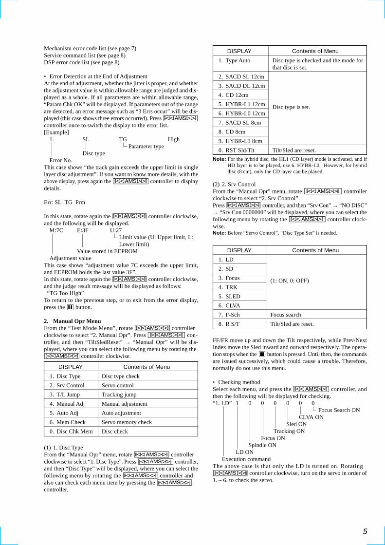
5
Mechanism error code list (see page 7)Service command list (see page 8)DSP error code list (see page 8)
• Error Detection at the End of AdjustmentAt the end of adjustment, whether the jitter is proper, and whetherthe adjustment value is within allowable range are judged and dis-played as a whole. If all parameters are within allowable range,“Param Chk OK” will be displayed. If parameters out of the rangeare detected, an error message such as “3 Errs occur” will be dis-played (this case shows three errors occurred). Press [ AMS ]controller once to switch the display to the error list.[Example]
1. SL TG HighParameter type
Disc typeError No.
This case shows “the track gain exceeds the upper limit in singlelayer disc adjustment”. If you want to know more details, with theabove display, press again the [ AMS ] controller to displaydetails.
Err: SL TG Prm
In this state, rotate again the [ AMS ] controller clockwise,and the following will be displayed.
M:7C E:3F U:27Limit value (U: Upper limit, L:Lower limit)
Value stored in EEPROMAdjustment value
This case shows “adjustment value 7C exceeds the upper limit,and EEPROM holds the last value 3F”.In this state, rotate again the [ AMS ] controller clockwise,and the judge result message will be displayed as follows: “TG Too High”To return to the previous step, or to exit from the error display,press the X button.
2. Manual Opr MenuFrom the “Test Mode Menu”, rotate [ AMS ] controllerclockwise to select “2. Manual Opr”. Press [ AMS ] con-troller, and then “TiltSledReset” → “Manual Opr” will be dis-played, where you can select the following menu by rotating the[ AMS ] controller clockwise.
DISPLAY Contents of Menu
1. Disc Type Disc type check
2. Srv Control Servo control
3. T/L Jump Tracking jump
4. Manual Adj Manual adjustment
5. Auto Adj Auto adjustment
6. Mem Check Servo memory check
0. Disc Chk Mem Disc check
(1) 1. Disc TypeFrom the “Manual Opr” menu, rotate [ AMS ] controllerclockwise to select “1. Disc Type”. Press [ AMS ] controller,and then “Disc Type” will be displayed, where you can select thefollowing menu by rotating the [ AMS ] controller andalso can check each menu item by pressing the [ AMS ]controller.
l L
l L
l Ll L
l L
DISPLAY Contents of Menu
1. Type Auto Disc type is checked and the mode forthat disc is set.
2. SACD SL 12cm
3. SACD DL 12cm
4. CD 12cm
5. HYBR-L1 12cm Disc type is set.6. HYBR-L0 12cm
7. SACD SL 8cm
8. CD 8cm
9. HYBR-L1 8cm
0. RST Sld/Tlt Tilt/Sled are reset.
Note: For the hybrid disc, the HL1 (CD layer) mode is activated, and ifHD layer is to be played, use 6. HYBR-L0. However, for hybriddisc (8 cm), only the CD layer can be played.
(2) 2. Srv ControlFrom the “Manual Opr” menu, rotate [ AMS ] controllerclockwise to select “2. Srv Control”.Press [ AMS ] controller, and then “Srv Con” → “NO DISC”→ “Srv Con 0000000” will be displayed, where you can select thefollowing menu by rotating the [ AMS ] controller clock-wise.Note: Before “Servo Control”, “Disc Type Set” is needed.
DISPLAY Contents of Menu
1. LD
2. SD
3. Focus (1: ON, 0: OFF)4. TRK
5. SLED
6. CLVA
7. F-Sch Focus search
8. R S/T Tilt/Sled are reset.
FF/FR move up and down the Tilt respectively, while Prev/NextIndex move the Sled inward and outward respectively. The opera-tion stops when the x button is pressed. Until then, the commandsare issued successively, which could cause a trouble. Therefore,normally do not use this menu.
• Checking methodSelect each menu, and press the [ AMS ] controller, andthen the following will be displayed for checking.“1. LD” 1 0 0 0 0 0 0
Focus Search ONCLVA ON
Sled ONTracking ON
Focus ONSpindle ON
LD ONExecution command
The above case is that only the LD is turned on. Rotating[ AMS ] controller clockwise, turn on the servo in order of1. – 6. to check the servo.
l L
l L
l L
l L
l L
l L
l L
l Ll L
l Ll L

6
Also, with the servo of 1. – 6. turned on, press the [CHECK] but-ton on the remote commander, so that you can check the disc type,jitter, etc. To return to original display, press the [CHECK] buttonagain.[Example]
SL 18 2A 020520Sector address
CLV statusJitter value
Disc typeCAUTION: In 7. F-Sch menu, the servo is not applied, thus causing opti-
cal system to be damaged if used together with other menu.Never use it.
(3) 3. T/L JumpThis adjustment is not normally used.
(4) 4. Manual AdjThis adjustment is not normally used.
(5) 5. Auto AdjThis adjustment is not normally used.
(6) 6. Mem CheckFrom the “Manual Opr” menu, rotate [ AMS ] controllerclockwise to select “6. Mem Check”. Press [ AMS ]controller, and then “EEPROM Data” will be displayed, whereyou can select the following menu by rotating the [ AMS ]controller clockwise.
DISPLAY Contents of Menu
CD
HYBR
SL Servo setting check
DL-L0
DL-L1
1 Select each menu and press [ AMS ] controller, andthen the contents of servo setting stored in the EEPROM willbe displayed.
2 The contents of servo setting are same as those in (7) 6.Memory Check of Auto Adjust menu. (See page 4)
3 In this menu, default value can be written to the EEPROM.Press the [CLEAR] buttonon on the Remote commander,“Deflt Set? Y/N” message will be displayed, and then press[ AMS ] controller. When “EepDfltSet” message is dis-played, default value can be written to the EEPROM. To can-cel default value setting, press the X button.
CAUTION: If you do “EepDfltSet”, after “EepDfltSet”, “Auto Adjust-ment” is needed. (see page 3)
(7) 7. Disc Chk MemFrom the “Manual Opr” menu, rotate [ AMS ] controllerclockwise to select “0. Disc Chk Mem”. Press [ AMS ]controller, and then “Disc Check” will be displayed, where youcan select the following menu by rotating the [ AMS ]controller clockwise.
DISPLAY Contents of Menu
1. SL Disc Chk
2. CD Disc Chk Disc Type Check
3. DL Disc Chk
0. Rst Sld/Tlt Tilt and Sled are reset.
• Select the menu 1. – 3. and press the [ AMS ] control-
ler, and “New 3D” will be displayed, and then each displaycorresponding to the selected menu 1. – 3. will return.
3. Mecha Aging MenuThis is the mechanism aging mode.From the “Test Mode Menu”, rotate [ AMS ] controllerclockwise to select “3. Mecha Aging”. Press [ AMS ] con- controller, and “Mecha Aging” → “Abort Stop Key” → “PressOpen Key” will be displayed. Press A button → G button inthis order, and the tray will be opened and closed repeatedly, andits count will be displayed. Up to 2,147,483,647 times can becounted. In such a case, the disc type is also checked.[Example]
C: 2526Number of counts
To quit this operation, press x and X buttons. (Simultaneously,the count is cleared.)
4. Emg History MenuFrom the “Test Mode Menu”, rotate [ AMS ] controllerclockwise to select “4. Emg History”. Press [ AMS ] con-troller, and “EMG History” message will be displayed. Rotatingthe [ AMS ] controller clockwise switches to the followingdisplay where the servo emergency history (1. – 10.) and the laserlighting hours are displayed.
1. 1F 060800002. 2F 060800003. 00 000000004. 00 000000005. 00 000000006. 00 000000007. 00 000000008. 00 000000009. 00 00000000
10. 00 00000000LASR 0hCD 0hSACD 0h
Clear History?
1 How to see code[Example]
11 06 04 C701History buffer 2byte DSP error code(see page 8)
History disc type (see page 8)Mechanism mode (see page 8)
Mechanism error code (see page 7)This case shows “DSP error, Spin up mode, SL 12cm, CLV un-lock at Sled ON”.Also, at this time, pressing [ AMS ] controller causes allemergency information (16 bytes) to be displayed every 4 bytesfor 4 items.[Example]
1-1 00000000Emergency information 1
Item No.: Variable each time the [ AMS ] controller ispressed
2 Laser lighting hours[Example]
LASR 14hCD 6hSACD 8h
LASR displayed value is the total of CD and SACD laser lightinghours. (The time less than minutes is omitted.)
l Ll L
l L
l L
l Ll L
l L
l L
l Ll L
l L
l L
l L
l L
l L
l L

7
3 History clear• How to clear all history dataFor the items with “Clear History?” message, press [ AMS ]controller, and all emergency history data and all laser lightinghours are cleared to 0.
• How to clear individual data1 Emergency history clearPress [DISPLAY MODE], [CLEAR] buttons on the remote com-mander in this order.
2 Laser lighting hour clearPress [SACD/CD], [CLEAR] buttons on the remote commanderin this order.
3 Setup clearPress [REPEAT], [CLEAR] buttons on the remote commander inthis order.Five backup data of [PLAY MODE], [CLEAR], [SACD/CD],[TIME/TEXT], [DIGITAL FILTER] are cleared to the initial data.
5. Ver Info MenuFrom the “Test Mode Menu”, rotate [ AMS ] controllerclockwise to select “5. Ver Info”. Press[ AMS ] control-ler, and “Version Info” message will be displayed. Rotating the[ AMS ] controller clockwise switches to the following dis-play where the ROM version, date of creation, servo DSP version,and checksum are displayed.[Example]
V1.00 00/02/14SrvDSP 1.000RomCsum 711C
6. RF Jit DispFrom the “Test Mode Menu”, rotate [ AMS ] controllerclockwise to select “6. RF Jit Disp”. Press [ AMS ] control-ler, and then “Set Disc” message will be displayed. Set a disc andpress [ AMS ] controller, and “Sinup...” will be displayed,then the jitter will be measured and displayed. To exit from thismode, press the X button. <Jitter measurement and display example>
CD 22 2A 000000Sector address
CLV statusJitter value
Disc type (auto check)SL : Single layer discHC : Hybrid layer disc, CD layerHD: Hybrid layer disc, SACD layerDL : Dual layer discCD : CD disc1 The disc type is checked automatically.2 For a hybrid disc, rotating the [ AMS ] controller can
switch the layer during jitter adjustment. Also, rotating the[ AMS ] controller can jump to inner track, middle track,or outer track.However, the address is fixed. Music cannot besearched. For a dual layer disc, a jump between layers is pos-sible.1. Play HD-HL02. Play CD-HL13. Jp Md1 Track4. Jp Inn Track5. Jp Out Track6. Jp DL0 -> DL17. Jp DL1 -> DL0
3 Press A button to change the disc.
l L
l L
l L
l L
l L
7. PDM Mode MenuThis mode is not normally used.
8. CDM Adj MenuThis mode is not normally used.
9. Set Up Init MenuFrom the “Test Mode Menu”, rotate [ AMS ] controllerclockwise to select “7. Set Up Init”. Press [ AMS ]controller, and “Initialized” will be displayed, then “Reset? Y/N”will be displayed. Press again [ AMS ] controller, and“Restart ...” will be displayed, and then the player will be resetand restarted. (At the restart, the set exits from the Test mode.)
10. Sld Ship Pos MenuMoving sled the fuctory set up position.
Mechanism error code
EmergencyCategory Emergancy Name Code
Electrical SSI ERR 10DSP ERR 11EEP ERR 12EEP HOURS METER WRITE ERR 13DSP BUSY TIME OUT 14EEP CHECK SUM NG 15DSP BUSY TIME OUT ESCAPE 16
Mechanism TILT SLED RESET NG 20TILT MOVE NG 21TILT REQ POSI NG 22SLED MOVE NG 23SLED REQ POSI NG 24
Adjustment ADJ TRK BAL NG 30ADJ TRK GAIN 31ADJ FCS BAL NG 32ADJ FCS BIAS NG 33ADJ FCS GAIN 34ADJ TILT NG 35ADJ EQ BOOST NG 36ADJ GD NG 37ADJ LAST JITTER NG 38ADJ GAIN RANGE OVER 3F
Focus FOCUS NG F1FOCUS JUMP COUNT OVER 41
Spindle CLV LOCK NG 1FSPDL BRAKE COUNT OVER 51
Sheek SACD REQ ADR NG 60CD REQ ADR NG 61CD REQ INDEX NG 62SACD SEEK COUNT OVER 63CD SA SEARCH COUNT OVER 64CD INDEX SEARCH COUNT OVER 65
Date SACD INFO NG 70CD INFO TIME OUT 71
Other RECOVERY DISC CHECK NG DFRECOVERY COUNT OVER 81DISC CHECK ERR DFDISC CHECK TIME OUT 83INVALID CMD CODE 84INVALID CMD 85DUMMY JOB 86NEXT MODE NONE 87
l L
l L
l L
l L
l L
l L
l L

8
History disc type
Display Contents
0x00 TBD0x01 CheckErr0x02 NoDisc0x03 SacdSl080x04 SacdSl120x05 SacdDl080x06 SacdDl120x07 Cd080x08 Cd120x09 Hl080x0a Hl12
0x: Hex.
Mechanism mode
Display Contents
0x00 Reset0x01 DriveInit0x02 PonReady0x03 MechInit0x04 Stop0x05 DiscCheck0x06 SpinUp0x07 SpinDown0x08 Seek0x09 Trace0x0a Pause0x0b Recovery0x0c RecoDc0x0d SrvcStop0x0e Srvc
0x: Hex.
Self diagnosis error code
Display Contents
00 Normal end01 SRAM Read/Write NG02 HGA NG03 EEPROM NG04 ARP Resister NG05 ARP DATA BUS NG06 ARP ADDRESS BUS NG07 ARP RAM Read/Write NG08 Servo DSP Resister NG09 SACD CHIP DRAM NG10 SACD CHIP DRAM TIME OUT11 SACD CHIP BUS NG12 SDBUS NG13 SDBUS TIME OUT
Service command
Display Contents code
Tray Open Tray open 01Tray Close Tray close 02Set Disc Type Set Disc Type 03Sled Go Home Sled move Home position 04Tilt Go Home Tilt move Home Position 05Sled Tilt Reset Sled/Tilt Reset 06Tray Down Tray chuck Down 07All Servo Stop All Servo stop 10Ld On Laser diode ON 11Ld Off Laser diode OFF 12Focus Search Focus Search 13Focus Off Focus Servo OFF 14Focus Search On Focus Servo ON 15Tracking On Tracking Servo ON 17Tracking Off Tracking Servo OFF 18Sled On Sled Servo ON 19Sled Off Sled Servo OFF 1ASled Move Fwd Sled Move Foward 1BSled Move Rev Sled Move Reverse 1CSled Direct Move Sled Direct Move 1DSpdl Start disc size cheking and
spendle start 20Spdl Stop Spingdle stop 21Cav On Spindle with
normal speed ON 22Clva On CLVA Servo ON 26Tilt Move Down Tilt Move Down 2BTilt Move Up Tilt Move Up 2CTilt Direct Move Tilt Direct Move 2DLj (L0 -> L1) LayerJump
(Tracking/Sled Servo ON) 3ALj (L1 -> L0) 3BFj (L0 -> L1) FocusJump
(Tracking/Sled Servo OFF) 3CFj (L1 -> L0) 3D
DSP error codeTask code (Upper Column)
Code* Contents
2 Traking balance adjustment3 Focus Search4 Focus jump5 Traking ON6 1, 2 Track jump7 Middle Track jump8 Large Track jump9 Sled movec Sled ONd Sereal
*Code: Hex.
Error code (Lower column)
Code* Contents
2 Sequence Command in Sequence3 Invalid Parameter4 Sequence Stop by “time out”5 Sequence Stop except “time out”6 Not FOK7 Not LOCK8 Servo ON in servo ON9 Defect Continuation Detecta Focus OFFb Tracking OFFc ACK Error
*Code: Hex.

99
SCD-XB940
2. DIAGRAMS
2-1. BLOCK DIAGRAM – RF/SERVO Section –
1
5678
13141516
1211109
20
19
17
23
1413
23
5
9
6
7
1615
2326
20
INVERTERQ601
LASERDIODE
46454443
44
69
22
434241
68
48
39
40
29 67
28
DETECTOR
OPTICAL PICK-UPBLOCK
(KHM-220AAA/JIN)
AUTOMATICPOWER
CONTROLQ001
32
85
48
66
97
26
39
321
23 65 7 9 8 50
27
DEFECTSWITCH
Q002
(FOCUS)(TRACKING)
2-AXISDEVICE
VC(2.5V)
FOCUSCOIL
DRIVE
TE GAINCONTROL AMP
IC610 (1/2)TILTMOTORDRIVE
SPINDLEMOTORDRIVE
SPINDLEERROR AMPIC613 (1/2)
LOADINGMOTORDRIVE
15 –
18
STANDBY
STANDBY
STANDBY
STANDBY
TRACKINGCOIL
DRIVE
M
M
4, 5
117
– 12
0, 1
22 –
125
60 –
64
74, 8
1, 8
4, 9
3, 9
6
1211
FCS+FCS–
TRK+TRK–
INLIMITSENSOR
2
5
20
9
231718
6
MSLED
MOTORDRIVE
11, 1
213
, 14
M
SPM+SPM–
LDM+LDM–
7 5
10
3
8
1
46
49
92
80
RF
ABCD
EFGH
RFIP
A2B2C2D2
EF
GH
ABCD
47
54
5859
64
63
61
62
50
49
51
52
20
2126
42
2831
38
SDENSRDSWDSCLK
HOLD1
TE
FE
PI
MIN
TZC
SIGDET
SIGO
MIRR
HOLD2
DFT
25
LDON
LD
PD
VC
VC1
LD
PD
2VC
(SPINDLE)
(TILT)
(SLED)
M1(LOADING)
CENTER VOLTAGEGENERATORIC613 (2/2)
2.5VC
2VC
1.6V
DVD RF, CDRF
+5V+3.3V
CENTER VOLTAGEGENERATORIC610 (2/2)
57
+3.3V
2VC
4
3
2
1
GIO5
ADC0
GIO6GIO7GIO8
ADC1
ADC2
DAB2
GIO2
ADC3
DAB0
GIO4
GIO1
DAB1
DAB3
TRREF
TRIN
DFCT1
GIO11
DIGITAL SERVOSIGNAL PROCESSOR
IC607
FDCH
GFCD+
TLTB
TE GAIN
TRD+
TLTA
TRD–
FCD–
SSDFCT
INLIMSP ERROR
LOCK
MCK1
LOCK, MCK1
MCKX601
27MHZ
FGAEF
X1
RS
GIO10
HINTHCS
HMR
EA0,
1HD
0 –
7AD
C5 –
9
X2
VRBA
, VRB
I – 3
,VR
TO
HRD
TIA+, – TIB+, –
FCD+FCD–
TRD+TRD–
TILTATILTB
SLB–, +
SLA–, +
HD8 – 15
5
6
7
8
9
11
12
14
HA0, 1
HD0 – 15
HD0 – 19
XSDPRDXSDPWRXSDPCSXSDPINT
GAIN CONTROLQ601, 602
S1(OPEN/CLOSE)
OCSW1
OCSW2
13
10
15
XSDPRD, XSDPWR,XSDPCS, XSDPINT
FCSON
XSDPRST
RSTX
SPGAIN
LDMM/DMM, LDMP/DMP
XDRV MUTE
SDPLSTOP
OCSW1, OCSW2
D604
D600
D606 (2/2)D610
MDSOMDPO
D609
FGIN
ADC4
PWM
2PW
M0
PWM
1
STVC
SLDA
SLDB
GIO0
D606(1/2)
D608
LDMM/DMM
LDMP/DMP
26
3
STVC
STVCSLDB
SLDA
D607
D605
108
109
128
FOCUS/TRACKING COIL DRIVE,TILT MOTOR DRIVE
IC614
SPINDLE/SLED/LOADINGMOTOR DRIVE
IC615
ATOP
ATON
AIP
AIN
SSOUT
FNP
FNN
CLM
DIP
DIN(Page 10)
(Page 11)
(Page 11)
(Page 10)
(Page 11)
(Page 11)
(Page 11)
(Page 11)
(Page 11)
(Page 10)
(Page 11)
(Page 11)
(Page 11)
(Page 11)
(Page 11)
DATA BUS
ADDRESS BUS
SACD/CD RF AMP,FOBUS/TRACKING ERROR AMP
IC001
• SIGNAL PATH
: SACD
: CD
05

1010
SCD-XB940
19
1327142829
58
29
5121
4952
113111
5556
596061
868783
123
84
MA0
– 9
16 –
19,
22
– 26
97, 9
8, 1
00 –
105
63 –
68,
70,
71
73 –
76,
79
– 82
COAXIAL
OPTICAL
OPTICALTRANCEIVER
IC352
IC352
BUFFERQ351
DIGITAL OUTCD
J351
107108109
148152151150
9193959496
18
52
1001
11
9
91 –
98
SD0
– 7
9 –
16
82 –
89
WAD
0 –
7
1(Page 9)
24(Page 11)
2(Page 9)
11(Page 9)
23(Page 11)
22(Page 11)
21(Page 11)
20(Page 11)
19(Page 11)
SWITCHINGIC616 (1/2)
SWITCHINGIC616 (2/2)
SWITCHINGIC627
SWITCHINGIC629
SWITCHINGIC630
80
81
22
17(Page 11)
16(Page 11)
05
18(Page 11)
6
13
WCK
WRFD
TRSTXRST
7 8 9 10 11
XMSL
ATM
SCK
MSD
IM
SDO
MSR
EDY
14
Q
DCK
Q
Q Q
DCK
INVERTERIC624
28
27
256FSO IN
LT64FSO
SDATAL, SDATAR
CDDATA,
12
11
8
2
65
3
9
46
42
TIMINGIC621
69686766
XOE
BCKD
BCKA
XRASXCASXWE
227
236
48
2 –
5, 2
4 –
27
51, 5
2, 5
5 –
63
9 –
13, 1
6 –
21
70 –
77
47
SDATAR
SDATAL
DSAR
DSAL 26
25CDBCK, CDLRCK
(Page 12)
(Page 12)
(Page 12)
(Page 12)
17 110DVD RFCD RF
DVD RF, CD RF
D-RAMIC628
DQ1
– 16
A0 –
8
WEOE
RASUCASLCAS
HD0
– 15HD0 – 15
MA0 – 8
RFIN2
LOCKMCK1
MDSOMDPO
MD2MUTE
DFCTNORF
FWONXMRXRD
XWATXRSTXINT
XCS
D0 –
7A0
– 7
XMWRXDEXRASXCAS
RFIN1
RF INLOCK
LOCK, MCK1
MDSO, MDPO
HD0 – 15
HD0 – 19
MD2, MUTE,DFCT, NORF
FWON, XARPWR,XARPRD, XARPCS
XARPWT, XARPRST, XARPINT
AVDRST
XCE
SHRMUT, SHRLT, SCK1, SOUT1, SIN1, SHRRDY
LOCKMCK1
MDSOMDSP
RF SIGNALDECODER
IC622
HD8 – 15
HA0 – 7
MD2MUTE
DFCTNORF
FWONXARPWRXARPRD
XARPWTXARPRSTXARPINT
XARPCS
SCKI
SD0
– 7
SDCKXSHDXSAKXSRQSDEF
RFD
PLCKO
DOUT
DATABCLKLRCK
CDDATACD BCKCD LRCK
DSD DECODERIC617
99 SDEFXSRQXSAKXSHDSDCK
ADIN
XCE CLK
D0 –
7
A/D CONVERTERIC620
A0 –
10
DQ0
– 7
D-RAMIC625
OERASCASWE
DQ0
– 7
A0 –
10
SHRMUT
SHRLT
SOUT1SIN1SHRRDY
SCK1
MCK
I
SMUT
E
XCE
DATA BUS
ADDRESS BUS
2 –
5, 7
– 1
0,31
– 3
4, 3
6 –
39
154
– 15
7, 1
59 –
162
,16
4 –
167,
169
– 1
7213
6 –
139,
141
– 1
44,
146,
147
COUNTERIC309
CLOCKIC623
• SIGNAL PATH
: SACD
: CD
: DIGITAL OUT
2-2. BLOCK DIAGRAM – MAIN Section (1/2) –

1111
SCD-XB940
2-3. BLOCK DIAGRAM – MAIN Section (2/2) –
59
117116118115
9998103102
104109110111
108
71
2223 3
106107
54
114
57
93
9192
64
94
105
63
24 8
25 1
6 33
74
5742
53 54
5 35
4 36
3 16
157 79156 26155 28
145 82144 83143 84
112 41
6
12
10 65113 17
125 39124 40
142 69135 71
141 66
146 – 148, 149 – 154 13 – 20, 22 – 29 1 – 9, 32 – 40D0 – 15 A0 – 17
85 – 100 1 – 3, 102 – 109, 111 – 118, 120D16 – 31 A00 – 19
7 – 10, 13 – 16,29 – 32, 35 – 38
1 – 5, 18 – 21,24 – 27, 42 – 44
I/O0 – 15 A0 – 15
126 – 133
HD0 – 7 HA17 – 19, HA0 – 5
63
586039383762
21
22
2019
1817
6
7
40
41
17
22
23
16
32
33
3
6
7
8
10
13
14
15
12
24
21
20
19
18
31
30
9
29
DATA BUS4
ADDRESS BUS
DATA BUS
ADDRESS BUS5
(Page 9) (Page 10)
(Page 10)
(Page 10)
(Page 10)
(Page 12)
(Page 12)
(Page 9)
(Page 9)
(Page 9)
(Page 9)
(Page 9)
(Page 9)
(Page 9)
(Page 9)
(Page 9)
(Page 9)
(Page 10)
(Page 10)
(Page 10)
(Page 10)
(Page 10)
(Page 13)
(Page 13)
(Page 9)
(Page 13)
05
IFSI0, IFSO0, IFSCO, XVIFCS
RSTX
XFRRST
IFBSY
AVDRST AVDRSTXARPINT
XARPRSTXARPWT
XARPCSXARPRDXARPWR
FWON
NORFDFCT
MUTEMD2
OCSW2OCSW1
LDMP/DMPLDMM/DMM
XSDPINTXSDPCS
XSDPWRXSDPRD
XARPWT, XARPRST,XARPINT
FWON, XARPWR,XARPRD, XARPCS
MD2, MUTE,DFCT, NORF
LOCK
SPGAIN
OCSW1, OCSW2
XDRV MUTE
SPDLSTOP
XSDPRST
FCSON
XSDPRD, XSDPWR,XSDPCS, XSDPINT
MCK
LDMM/DMM,LDMP/DMP
HD0 – 15
HD8 – 15 HD0 – 15 HD0 – 16 HD0 – 15HA1 – 16 HA1 – 18 HA0 – 19HA0 – 5,HA17 – 19
HA0 – 19
MCK
SDSPRDSDSPWRSDPCSSDPIT
MD2MUTEDFCTNORF
FWONARPWRARPRDARPCS
ARPWT
AVDRST
XIFINT
ARPRSTARPINT
FCSON
SDPRST
SPDLSTOP
XDRVMUTE
LDMM/DMMLDMP/DMP
OCSW1
SPGAIN
LOCK
OCSW2
XECS
XEWC
XEBSY
DO
DI
SK
CS
WC
R/B
RST
WAITHINT1HINT3
HRDHWRHHWRL
XRAMDE
XRAMWE
RAMLBRAMUB
CS4CPUCK
CS1
EXPANDERIC612
S-RAMIC609
ROMIC632
OE
CS
WE
LBUB
XOE
XCE
HD0 – 15
HA0 – 19
OU0
RSTX
CSOL
SO0
SC0
TRG0
RDYINT1INT3
RXDWR0XWR1X
CS0X
CS4XCLK
CS1X
SC2
WD1X
CS0HRAS1
SC1SO1SI1
CS1H
OCPA1
OCPA2
OCPA0CS7X
CS6XTRG1
XCE
SHRMUTSHRLTSCK1SOUT1SIN1SHRRDY
INITLATCHSHIFT
DATAMODE
A22
A23
SI2
SO2
SC2
CTS
XDIAGON
SI2
SO2
JIGCLK
CTS
DIAGN
RXD
TXD
SYSTEMCONTROLLER
IC605
X1 X0
X60012.5MHz
XCE, SHRMUT, SHRLT
SHRMUT, SHRLT, SCK1,SOUT1, SIN1, SHRRDY
INIT, LATCH, SHIFT,DATA, MODE
AMUTEZ
CN600
(FOR CHECK)
EEPROMIC600
SWITCHINGIC606 (1/3)
SWITCHINGIC606 (2/3)
SWITCHINGIC606 (3/3)
IFSI0
IFSO0
IFSCO
XVIFCS

1212
SCD-XB940
2-4. BLOCK DIAGRAM – AUDIO Section –
212
2827
13
6
513
2
1
7
76
13
22827
2524 5
4
21
SWITCHINGCIRCUIT
SWITCHINGCIRCUIT
CONTROLCIRCUIT
PHONE LEVEL
CONSTANTCURRENTCIRCUIT
CONTROLCIRCUIT
CONSTANTCURRENTCIRCUIT
484950
53
52
6
71
2
35
6
7
1
10
5 7
15
18
4524
258
51
302831323334
1719
2224
15
1810X321
45MHZ
12 13
XOUT XIN
44
MUTINGCONTROL
Q303
RV601-1
PHONES J601
ANALOG OUTJ301
PHONE LEVELRV601-2
RELAYDRIVE
Q301, Q302
5
CD DATA,CD BCK,CD LRCK
SDATA L, SDATA R
LT64FSO
DIGITAL FILTER,D/A CONVERTER
IC301
CD DATACD BCKCD LRCK
SDATA L
SDATA R
256FSO IN
INIT
LATCH
SHIFTDATA
MODE
(Page 10)
INIT, LATCH,SHIFT, DATA, MODE
IN2–IN2+
IN1+IN1–
VEE1VCC1
I01+I02–
I01–I02+
+7V –7V
CIREF
+5V
CURRENT PULSEIC401
CURRENT PULSEIC501
I-VCONVERSION
IC402 AUDIO FILTERIC403 (1/2) AUDIO FILTER
IC403 (2/2)
RY301
HEADPHONEAMP
IC331 (1/2)
+7V –7V
+5V
IN2– IO1+IO2–
IO1–IO2+
IN2+
IN1+IN1–
VCC1 VEE1
I-VCONVERSION
IC502 AUDIO FILTERIC503 (1/2) AUDIO FILTER
IC503 (2/2)
HEAD PHONEAMP
IC331 (2/2)
R
L
DATAIBCKILRCKI
SDATA L
SDATA R
SBCKI
INITNREGCLRLATCHSHIFTSCDATAMODE
LVCK02
L1 (–)L1 (+)
L2 (+)L2 (–)
R2 (–)R2 (+)
R1 (+)R1 (–)
AMUTEZ
25
(Page 10) 26
(Page 10)
(Page 10)
27
28
(Page 11) 32
(Page 11) 33
CIREF
• SIGNAL PATH
: SACD
: CD05
MUTINGQ403
MUTINGQ503

1313
SCD-XB940
47 51
52
53
46
6335
62
64
61
44
4143
32
30
50
494860
56
31
1 –
3439
– 5
253
, 54
P1 –
34
3G –
16G
1G, 2
G
31
29
ROTARYENCODERS201 (1/2)
SEGMENTDRIVEQ201
GRIDDRIVE
Q202, 203
–33VREGULATOR
Q921
+12VREGULATOR
IC905
+12VREGULATOR
IC907
+5VREGULATOR
IC906
+5VREGULATOR
IC903
LINEFILTERL901
+3.3VREGULATOR
IC904
+3.3VREGULATOR
IC306
+5VREGULATOR
IC303
+3.3VREGULATOR
IC619
+5VREGULATOR
IC302
+7VREGULATOR
IC304
–7VREGULATOR
IC305
+12VREGULATOR
IC307
–12VREGULATOR
IC308
REMOTECONTROLRECEIVER
IC202
RESETSIGNAL
GENERATORIC271
IFBSY(Page 11)
(Page 11)
+5V
IFSI0, IFSO0, IFSCO, XIFCS
XFRRSTD201
IFSI0
IFSO0IFSCOXIFCS
ACK
RESET
SOUT
SINSCKREQ
SIRCS
CP
CS
DA
RESET OUT
KEY 0
JOG2JOG1
EXTAL XTAL
DISPLAY CONTROLLERIC203
FLUORESCENTINDICATOR TUBE DRIVE
IC201
X2018MHz
FL CLK
FLT
FL DATA
FL RST
P35
S201 (2/2),S251 – 254
F1
F2
FLUORESCENTINDICATOR
TUBEFL201
POWER TRANSFORMER(DIGITAL)
T901
F1, F2
RECTD917 – 920
RECTD913 – 916
RECTD909 – 912
RECTD905 – 908
RECTD901 – 904
+5V
–33V
TODISPLAYSECTION
+12V(M +12V)
+12V
+5V
+3.3V
POWER
S901
AC IN
POWER TRANSFORMER(ANALOG)
T902
+5V(D +5V)
+3.3V
+5V
+5V
+7V
–7V
+12V
–12V
AUDIOSECTION
+3.3VRF SIGNAL DECODER
(IC622)
RF, MAINSECTION
30(Page 11)
05
2-5. BLOCK DIAGRAM – DISPLAY/POWER SUPPLY Section –

1414
2-6. IC PIN FUNCTION DESCRIPTION• MAIN BOARD IC605 MB91107PFV-G-BND (SYSTEM CONTROLLER)
Pin No. Pin Name I/O Description
1, 2 O Address signal output to the expander (IC612) and ROM (IC632)
3 A19/P63 O Address signal output to the expander (IC612)
4, 5 O Address signal output terminal Not used (open)
6, 7 O Test signal output terminal for check (fixed at “H” in this set)
8 A24/P70 O Address signal output terminal (fixed at “H” in this set)
9 AVCC — Power supply terminal (+3.3V) (for A/D converter)
10 AVRH — Reference voltage input (high) terminal (for A/D converter)
11 AVSS/AVRL — Ground terminal (for A/D converter) and Reference voltage input (low) terminal
12 to 15 AN0 to AN3 I Analog input terminal (for A/D converter)
16 TRG0/PH0 O Reset signal output to the expander (IC612) “L”: reset
17 TRG1/PH1 O SACD/CD mode signal output to the digital filter (IC301)
18 TRG2/PH2/CS6X O Serial data output to the digital filter (IC301)
19 TRG3/PH3/CS7X O Shift signal output to the digital filter (IC301)
20 OCPA0/PH4 O Latch signal output to the digital filter (IC301)
21 OCPA1/PH5 O Initial signal output to the digital filter (IC301)
22 OCPA2/PH6 O Audio muting signal output terminal “L”: muting
23 OCPA3/PH7 O Filter control signal output terminal
24 VCC — Power supply terminal (+3.3V) (digital system)
25 INT0/PG0 I External interrupt request signal input terminal Not used (fixed at “H”)
26 INT1/PG1 I Interrupt request 1 signal input from the expander (IC612)
27 INT2/PG2 I External interrupt request signal input terminal Not used (fixed at “H”)
28 INT3/PG3 I Interrupt request 3 signal input from the expander (IC612)
29 to 32 I External interrupt request signal input terminal Not used (fixed at “H”)
33 SI0/RF0 I Serial data input from the display controller (IC203) and EEPROM (IC600)
34 VSS — Ground terminal (digital system)
35 SO0/PF1 O Serial data output to the display controller (IC203) and EEPROM (IC600)
36 SC0/PF2 O Clock signal output to the display controller (IC203) and EEPROM (IC600)
37 SI1/PF3 I Serial data input from the DSD decoder (IC617)
38 SO1/PF4 O Serial data output to the DSD decoder (IC617)
39 SC1/PF5 O Clock signal output to the DSD decoder (IC617)
40 SI2/PF6 I Serial data input terminal for check
41 SO2/PF7 O Serial data output terminal for check
42 SC2/PE0 O Clock signal output terminal for check
43 DREQ0/PE1 I External transfer request signal input terminal
44 DACK0/PE2 O External transfer request acknowledge signal output terminal
45 EOP0/PE3 O Not used (open)
46 DREQ1/PE4 I External transfer request signal input terminal Not used (fixed at “H”)
47 DACK1/PE5 O External transfer request acknowledge signal output terminal Not used (fixed at “H”)
48 EOP1/PE6 O Not used (open)
49 DREQ2/PE7 I External transfer request signal input terminal Not used (open)
50 DACK2/PI0 O External transfer request acknowledge signal output terminal Not used (open)
51 EOP2/PI1/ATGX O Not used (open)
A17/P61, A18/P62
A20/P64, A21/P65
A22/P66, A23/P67
INT4/PG4 to INT7/PG7
Pin No. Pin Name I/O Description
52 VSS — Ground terminal (digital system)
53 X1 O System clock output terminal (12.5MHz)
54 X0 I System clock input terminal (12.5MHz)
55 VCC — Power supply terminal (+3.3V) (digital system)
56 RAS0/PB0 O Control signal output terminal Not used (fixed at “H”)
57 CS0L/PB1 O Interrupt request signal output to the display controller (IC203)
58 CS0H/PB2 O Muting signal output to the DSD decoder (IC617) “L”: muting
59 DW0X/PB3 O Not used (open)
60 RAS1/PB4 O Latch signal output to the DSD decoder (IC617)
61 CS1L/PB5 O Not used (open)
62 CS1H/PB6 I Ready signal input from the DSD decoder (IC617) “L”: ready
63 DW1X/PB7 O Write enable signal output terminal “L”: active
64 C — Bypass capacitor terminal for internal capacitor
65 CS0X O Chip select signal output to the ROM (IC632) “L”: active
66 CS1X/PA1 O Chip select signal output to the expander (IC612) and S-RAM (IC632) “L”: active
67, 68 O Chip select signal output terminal “L”: active (fixed at “H” in this set)
69 CS4X/PA4 O Chip select signal output to the expander (IC612) “L”: active
70 CS5X/PA5 O Chip select signal output terminal “L”: active (fixed at “H” in this set)
71 CLK/PA6 O Clock signal output to the expander (IC612)
72 NMIX I Non maskable interrupt signal input terminal “L”: active (fixed at “H” in this set)
73 HSTX I Hardware standby signal input terminal “L”: active (fixed at “H” in this set)
74 RSTX I Reset signal input from the display controller (IC203)
75 VSS — Ground terminal (digital system)
76 MD0 I Mode set signal input terminal (fixed at “H”)
77, 78 MD1, MD2 I Mode set signal input terminal (fixed at “L”)
79 RDY/P80 I Wait signal input from the expander (IC612)
80 BGRNTX/P81 O External bus release acknowledge signal output terminal (fixed at “H” in this set)
81 BRQ/P82 I External bus release request signal input terminal (fixed at “L” in this set)
82 RDX O Read strobe signal output to the expander (IC612)
83 WR0X O Write strobe 0 signal output to the expander (IC612)
84 WR1X/P85 O Write strobe 1 signal output to the expander (IC612)
85 to 92 I/O Two-way data bus with the S-RAM (IC609) and ROM (IC632)
93 to 100 D24 to D31 I/OTwo-way data bus with the servo digital signal processor (IC607), S-RAM (IC609), expander (IC612) , RF signal decoder (IC622), and ROM (IC632)
101 VSS — Ground terminal (digital system)
102 A00 OAddress signal output to the servo digital signal processor (IC607), expander (IC612) , and RF signal decoder (IC622)
103 A01 OAddress signal output to the servo digital signal processor (IC607), S-RAM (IC609), expander (IC612) , RF signal decoder (IC622), and ROM (IC632)
104 to 107 A02 to A05 OAddress signal output to the S-RAM (IC609), expander (IC612), RF signal decoder (IC622), and ROM (IC632)
108, 109 A06, A07 O Address signal output to the S-RAM (IC609), RF signal decoder (IC622), and ROM (IC632)
110 VCC — Power supply terminal (+3.3V) (digital system)
111 to 118 A08 to A15 O Address signal output to the S-RAM (IC609) and ROM (IC632)
119 VSS — Ground terminal (digital system)
120 A16/P60 O Address signal output to the S-RAM (IC609) and ROM (IC632)
CS2X/PA2, CS3X/PA3
D16/P20 to D23/P27

15
• MAIN BOARD IC607 CXD8791AQ (DIGITAL SERVO SIGNAL PROCESSOR)
Pin No. Pin Name I/O Description
1 HRD/HRXD I Data read strobe signal input from the expander (IC612)
2 HWR/HFS I Data write strobe signal input from the expander (IC612)
3 HCS I Chip select signal input from the expander (IC612)
4, 5 HA1, HA0/HCK I Address signal input from the system controller (IC605)
6 VDD — Power supply terminal (+3.3V) (digital system)
7 to 9 PWM0 to PWM2 O Sled motor control signal output to the sled motor drive (IC615)
10 VSS — Ground terminal (digital system)
11, 12 EMU1, EMU0 I/O Emulator signal input/output terminal Not used (open)
13 TDO O Test data output terminal Not used (open)
14 TCK I Test clock input terminal Not used (open)
15 TDI I Test data input terminal Not used (open)
16 TMS I Test mode select signal input terminal Not used (open)
17 TRST I Test reset signal input terminal Not used (open)
18 VDD — Power supply terminal (+3.3V) (digital system)
19 VSS — Ground terminal (digital system)
20 TRREF I Tracking reference signal input from the SSI33P3722 (IC001)
21 TRIN I Mirror detect signal input from the SSI33P3722 (IC001)
22 FGREF I FG reference clock signal input from the RF signal decoder (IC622)
23 FGIN I FG signal input terminal
24 PGREF I PG reference signal input terminal Not used (open)
25 PGIN I PG signal input terminal Not used (open)
26 RS I Reset signal input from the expander (IC612)
27 LG I Not used (open)
28 DFCT1 I Defect signal input terminal
29 HEAD I Head signal input terminal Not used (open)
30 CLKODIS I CLKOUT1 (pin ea ) disable signal input terminal “H”: disable (fixed at “L” in this set)
31 CLKOUT1 O Master clock output terminal Not used (open)
32 VDD — Power supply terminal (+3.3V) (digital system)
33 VSS — Ground terminal (digital system)
34 to 37 GIO15 to GIO12 — Not used (open)
38 GIO11 O Defect control signal output terminal
39 GIO10 O Function control signal input from the expander (IC612)
40 GIO9 — Not used (open)
41 GIO8 O Clock signal output to the SSI33P3722 (IC001)
42 GIO7 O Serial write data output to the SSI33P3722 (IC001)
43 GIO6/TMC2 I Serial read data input from the SSI33P3722 (IC001)
44 GIO5/TMC1 O Serial data enable output to the SSI33P3722 (IC001)
45 VDD — Power supply terminal (+3.3V) (digital system)
46 GIO4/TMC0 I Standby signal input from the tilt motor drive (IC614)
47 GIO3/INT5 — Not used (open)
48 GIO2/INT4 O Tilt motor control signal output to the tilt motor drive (IC614)
49 GIO1/INT3 O Tilt motor control signal output to the tilt motor drive (IC614)
50 GIO0/INT2 I Interrupt signal input terminal
51 VSS — Ground terminal (digital system)
52 TESTC I Test signal input terminal (fixed at “L”)
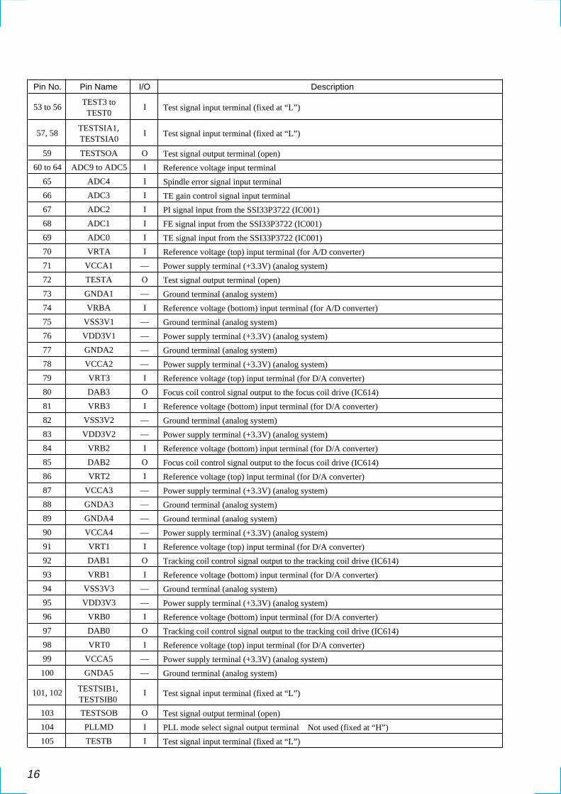
16
Pin No. Pin Name I/O Description
53 to 56 I Test signal input terminal (fixed at “L”)
57, 58 I Test signal input terminal (fixed at “L”)
59 TESTSOA O Test signal output terminal (open)
60 to 64 ADC9 to ADC5 I Reference voltage input terminal
65 ADC4 I Spindle error signal input terminal
66 ADC3 I TE gain control signal input terminal
67 ADC2 I PI signal input from the SSI33P3722 (IC001)
68 ADC1 I FE signal input from the SSI33P3722 (IC001)
69 ADC0 I TE signal input from the SSI33P3722 (IC001)
70 VRTA I Reference voltage (top) input terminal (for A/D converter)
71 VCCA1 — Power supply terminal (+3.3V) (analog system)
72 TESTA O Test signal output terminal (open)
73 GNDA1 — Ground terminal (analog system)
74 VRBA I Reference voltage (bottom) input terminal (for A/D converter)
75 VSS3V1 — Ground terminal (analog system)
76 VDD3V1 — Power supply terminal (+3.3V) (analog system)
77 GNDA2 — Ground terminal (analog system)
78 VCCA2 — Power supply terminal (+3.3V) (analog system)
79 VRT3 I Reference voltage (top) input terminal (for D/A converter)
80 DAB3 O Focus coil control signal output to the focus coil drive (IC614)
81 VRB3 I Reference voltage (bottom) input terminal (for D/A converter)
82 VSS3V2 — Ground terminal (analog system)
83 VDD3V2 — Power supply terminal (+3.3V) (analog system)
84 VRB2 I Reference voltage (bottom) input terminal (for D/A converter)
85 DAB2 O Focus coil control signal output to the focus coil drive (IC614)
86 VRT2 I Reference voltage (top) input terminal (for D/A converter)
87 VCCA3 — Power supply terminal (+3.3V) (analog system)
88 GNDA3 — Ground terminal (analog system)
89 GNDA4 — Ground terminal (analog system)
90 VCCA4 — Power supply terminal (+3.3V) (analog system)
91 VRT1 I Reference voltage (top) input terminal (for D/A converter)
92 DAB1 O Tracking coil control signal output to the tracking coil drive (IC614)
93 VRB1 I Reference voltage (bottom) input terminal (for D/A converter)
94 VSS3V3 — Ground terminal (analog system)
95 VDD3V3 — Power supply terminal (+3.3V) (analog system)
96 VRB0 I Reference voltage (bottom) input terminal (for D/A converter)
97 DAB0 O Tracking coil control signal output to the tracking coil drive (IC614)
98 VRT0 I Reference voltage (top) input terminal (for D/A converter)
99 VCCA5 — Power supply terminal (+3.3V) (analog system)
100 GNDA5 — Ground terminal (analog system)
101, 102 I Test signal input terminal (fixed at “L”)
103 TESTSOB O Test signal output terminal (open)
104 PLLMD I PLL mode select signal output terminal Not used (fixed at “H”)
105 TESTB I Test signal input terminal (fixed at “L”)
TESTSIA1, TESTSIA0
TEST3 to TEST0
TESTSIB1, TESTSIB0

17
Pin No. Pin Name I/O Description
106 VDD — Power supply terminal (+3.3V) (digital system)
107 VSS — Ground terminal (digital system)
108 X2/CLKIN I Clock input terminal (27MHz)
109 X1 O Clock output terminal (27MHz)
110 VDD — Power supply terminal (+3.3V) (digital system)
111 VSS — Ground terminal (digital system)
112 VCCA6 — Power supply terminal (+3.3V) (analog system)
113 LF I/O LF signal input/output terminal
114 GNDA6 — Ground terminal (analog system)
115 VDD — Power supply terminal (+3.3V) (digital system)
116 VSS — Ground terminal (digital system)
117 HD7/HIO I/OTwo-way data bus with the system controller (IC605), S-RAM (IC609), expander (IC612) , RF signal decoder (IC622), and ROM (IC632)
118 to 120 I/OTwo-way data bus with the system controller (IC605), S-RAM (IC609), expander (IC612) , RF signal decoder (IC622), and ROM (IC632)
121 VDD — Power supply terminal (+3.3V) (digital system)
122 to 125 I/OTwo-way data bus with the system controller (IC605), S-RAM (IC609), expander (IC612) , RF signal decoder (IC622), and ROM (IC632)
126 VSS — Ground terminal (digital system)
127 SRPRN I Parallel/serial mode select signal input terminal “L”: parallel mode (fixed at “L” in this set)
128 HINT/HTXD O Interrupt signal output to the expander (IC612)
HD6/HO6, HD4/HO4
HD3/HO3, HD0/HO0
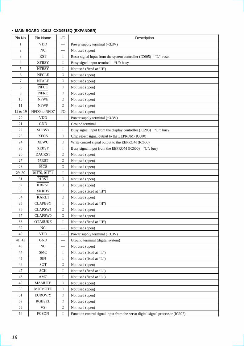
18
• MAIN BOARD IC612 CXD9515Q (EXPANDER)
Pin No. Pin Name I/O Description
1 VDD — Power supply terminal (+3.3V)
2 NC — Not used (open)
3 RST I Reset signal input from the system controller (IC605) “L”: reset
4 XFBSY I Busy signal input terminal “L”: busy
5 NFBSY I Not used (fixed at “H”)
6 NFCLE O Not used (open)
7 NFALE O Not used (open)
8 NFCE O Not used (open)
9 NFRE O Not used (open)
10 NFWE O Not used (open)
11 NFWP O Not used (open)
12 to 19 NFD0 to NFD7 I/O Not used (open)
20 VDD — Power supply terminal (+3.3V)
21 GND — Ground terminal
22 XIFBSY I Busy signal input from the display controller (IC203) “L”: busy
23 XECS O Chip select signal output to the EEPROM (IC600)
24 XEWC O Write control signal output to the EEPROM (IC600)
25 XEBSY I Busy signal input from the EEPROM (IC600) “L”: busy
26 DACRST O Not used (open)
27 57RST O Not used (open)
28 01CS O Not used (open)
29, 30 01IT0, 01IT1 I Not used (open)
31 01RST O Not used (open)
32 KRRST O Not used (open)
33 XKRDY I Not used (fixed at “H”)
34 KARLT O Not used (open)
35 CLAPBSY I Not used (fixed at “H”)
36 CLAPSW1 O Not used (open)
37 CLAPSW0 O Not used (open)
38 OTASUKE I Not used (fixed at “H”)
39 NC — Not used (open)
40 VDD — Power supply terminal (+3.3V)
41, 42 GND — Ground terminal (digital system)
43 NC — Not used (open)
44 SMC I Not used (fixed at “L”)
45 SIN I Not used (fixed at “L”)
46 SOT O Not used (open)
47 SCK I Not used (fixed at “L”)
48 AMC I Not used (fixed at “L”)
49 MAMUTE O Not used (open)
50 MICMUTE O Not used (open)
51 EUROV/Y O Not used (open)
52 RGBSEL O Not used (open)
53 VS O Not used (open)
54 FCSON I Function control signal input from the servo digital signal processor (IC607)
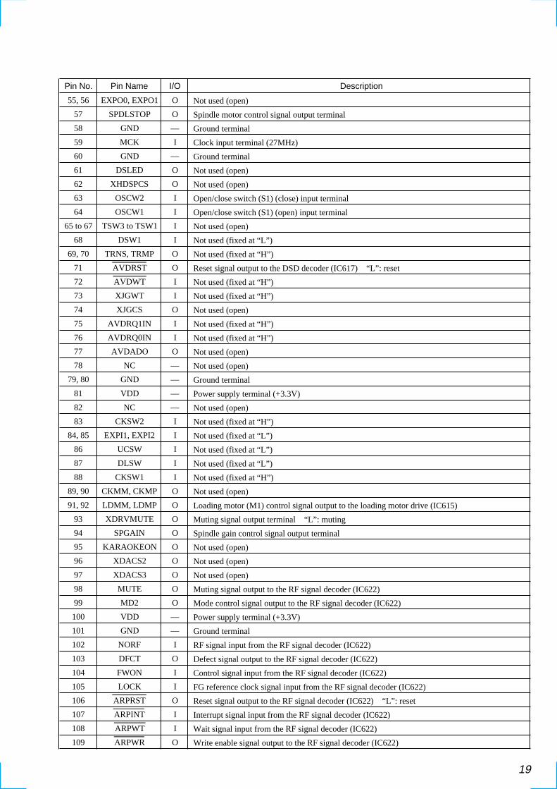
19
Pin No. Pin Name I/O Description
55, 56 EXPO0, EXPO1 O Not used (open)
57 SPDLSTOP O Spindle motor control signal output terminal
58 GND — Ground terminal
59 MCK I Clock input terminal (27MHz)
60 GND — Ground terminal
61 DSLED O Not used (open)
62 XHDSPCS O Not used (open)
63 OSCW2 I Open/close switch (S1) (close) input terminal
64 OSCW1 I Open/close switch (S1) (open) input terminal
65 to 67 TSW3 to TSW1 I Not used (open)
68 DSW1 I Not used (fixed at “L”)
69, 70 TRNS, TRMP O Not used (fixed at “H”)
71 AVDRST O Reset signal output to the DSD decoder (IC617) “L”: reset
72 AVDWT I Not used (fixed at “H”)
73 XJGWT I Not used (fixed at “H”)
74 XJGCS O Not used (open)
75 AVDRQ1IN I Not used (fixed at “H”)
76 AVDRQ0IN I Not used (fixed at “H”)
77 AVDADO O Not used (open)
78 NC — Not used (open)
79, 80 GND — Ground terminal
81 VDD — Power supply terminal (+3.3V)
82 NC — Not used (open)
83 CKSW2 I Not used (fixed at “H”)
84, 85 EXPI1, EXPI2 I Not used (fixed at “L”)
86 UCSW I Not used (fixed at “L”)
87 DLSW I Not used (fixed at “L”)
88 CKSW1 I Not used (fixed at “H”)
89, 90 CKMM, CKMP O Not used (open)
91, 92 LDMM, LDMP O Loading motor (M1) control signal output to the loading motor drive (IC615)
93 XDRVMUTE O Muting signal output terminal “L”: muting
94 SPGAIN O Spindle gain control signal output terminal
95 KARAOKEON O Not used (open)
96 XDACS2 O Not used (open)
97 XDACS3 O Not used (open)
98 MUTE O Muting signal output to the RF signal decoder (IC622)
99 MD2 O Mode control signal output to the RF signal decoder (IC622)
100 VDD — Power supply terminal (+3.3V)
101 GND — Ground terminal
102 NORF I RF signal input from the RF signal decoder (IC622)
103 DFCT O Defect signal output to the RF signal decoder (IC622)
104 FWON I Control signal input from the RF signal decoder (IC622)
105 LOCK I FG reference clock signal input from the RF signal decoder (IC622)
106 ARPRST O Reset signal output to the RF signal decoder (IC622) “L”: reset
107 ARPINT I Interrupt signal input from the RF signal decoder (IC622)
108 ARPWT I Wait signal input from the RF signal decoder (IC622)
109 ARPWR O Write enable signal output to the RF signal decoder (IC622)
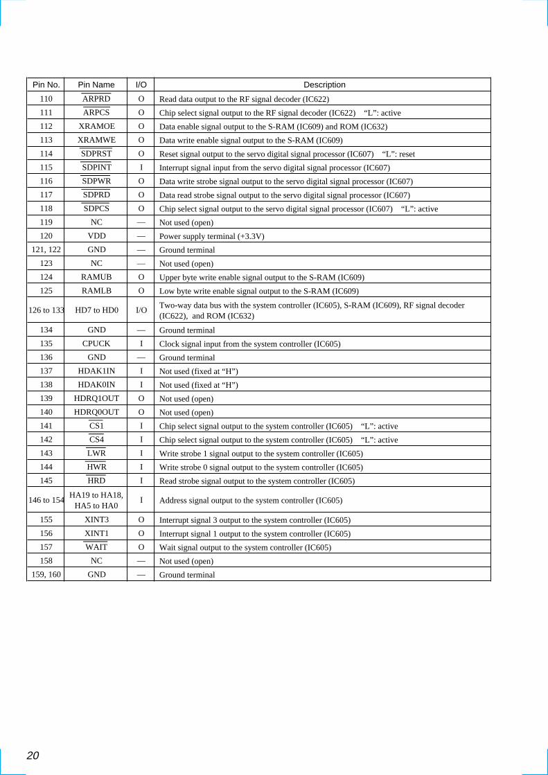
20
Pin No. Pin Name I/O Description
110 ARPRD O Read data output to the RF signal decoder (IC622)
111 ARPCS O Chip select signal output to the RF signal decoder (IC622) “L”: active
112 XRAMOE O Data enable signal output to the S-RAM (IC609) and ROM (IC632)
113 XRAMWE O Data write enable signal output to the S-RAM (IC609)
114 SDPRST O Reset signal output to the servo digital signal processor (IC607) “L”: reset
115 SDPINT I Interrupt signal input from the servo digital signal processor (IC607)
116 SDPWR O Data write strobe signal output to the servo digital signal processor (IC607)
117 SDPRD O Data read strobe signal output to the servo digital signal processor (IC607)
118 SDPCS O Chip select signal output to the servo digital signal processor (IC607) “L”: active
119 NC — Not used (open)
120 VDD — Power supply terminal (+3.3V)
121, 122 GND — Ground terminal
123 NC — Not used (open)
124 RAMUB O Upper byte write enable signal output to the S-RAM (IC609)
125 RAMLB O Low byte write enable signal output to the S-RAM (IC609)
126 to 133 HD7 to HD0 I/OTwo-way data bus with the system controller (IC605), S-RAM (IC609), RF signal decoder (IC622), and ROM (IC632)
134 GND — Ground terminal
135 CPUCK I Clock signal input from the system controller (IC605)
136 GND — Ground terminal
137 HDAK1IN I Not used (fixed at “H”)
138 HDAK0IN I Not used (fixed at “H”)
139 HDRQ1OUT O Not used (open)
140 HDRQ0OUT O Not used (open)
141 CS1 I Chip select signal output to the system controller (IC605) “L”: active
142 CS4 I Chip select signal output to the system controller (IC605) “L”: active
143 LWR I Write strobe 1 signal output to the system controller (IC605)
144 HWR I Write strobe 0 signal output to the system controller (IC605)
145 HRD I Read strobe signal output to the system controller (IC605)
146 to 154 I Address signal output to the system controller (IC605)
155 XINT3 O Interrupt signal 3 output to the system controller (IC605)
156 XINT1 O Interrupt signal 1 output to the system controller (IC605)
157 WAIT O Wait signal output to the system controller (IC605)
158 NC — Not used (open)
159, 160 GND — Ground terminal
HA19 to HA18, HA5 to HA0

21
Pin No. Pin Name I/O Description
1 XSRQ O Data request signal output to the RF signal decoder (IC622)
2 XSHD I Header flag signal input from the RF signal decoder (IC622)
3 VDD — Power supply terminal (+3.3V)
4 VSS — Ground terminal
5 SDCK I Serial data clock signal input from the RF signal decoder (IC622)
6 SMUTE I Muting signal input from the system controller (IC605) “L”: muting
7 XMSLAT I Latch signal input from the system controller (IC605)
8 MSCK I Clock signal input from the system controller (IC605)
9 MSDATI I Serial data input from the system controller (IC605)
10 MSDATO O Serial data output to the system controller (IC605)
11 MSREDY O Ready signal input from the system controller (IC605) “L”: ready
12 XMSDOE O Data enable signal output terminal Not used (open)
13 XRST I Reset signal input from the expander (IC612)
14 MCKI I Master clock signal input terminal
15 VSS — Ground terminal
16 CK75S I Master clock select signal input terminal “L”: 512fs, “H”: 768fs (fixed at “H” in this set)
17 EXCKO1 O External clock 1 signal output terminal Not used (open)
18 EXCKO2 O External clock 2 signal output terminal Not used (open)
19 LRCK I/O Clock signal input/output terminal (44.1kHz) Not used (open)
20 NC — Not used (open)
21 MNT2 O Monitor 2 signal output terminal Not used (open)
22 TRST I Reset signal input from the expander (IC612) “L”: reset
23 TCK I Clock signal input terminal for test (normally: fixed at “L”)
24 TDI I Data input terminal for test (normally: open)
25 TENA1 I Data enable signal input terminal for test (normally: open)
26 TDO O Data output terminal for test (normally: open)
27 VST — Ground terminal for test (normally: fixed at “L”)
28 VDD — Power supply terminal (+3.3V)
29 VSS — Ground terminal
30 MNT1 O Monitor 1 signal output terminal Not used (open)
31 MNT0 O Monitor 0 signal output terminal Not used (open)
32 XBIT O Monitor signal output terminal Not used (open)
33 F75HZ O Clock output terminal (75Hz) Not used (open)
34 SUPDAT O Serial data output terminal Not used (open)
35 XSUPAK O Data flag signal output terminal Not used (open)
36 SUPEN O Data enable signal output terminal Not used (open)
37 TEST1 I Test 1 signal input terminal for test (normally: fixed at “L”)
38 VSS — Ground terminal
39 TEST2 I Test 2 signal input terminal for test (normally: fixed at “L”)
40, 41 VSS — Ground terminal
42 BCKD I Phase reference signal input terminal
43 to 45 NC — Not used (open)
46 BCKA I Shift clock signal input terminal
47 DSAL O DSD data (Lch) output terminal
48 DSAR O DSD data (Rch) output terminal
49 ZDFLGL O Data (Lch) flag detect signal output terminal
• MAIN BOARD IC617 CXD2751Q (DSD DECODER)

22
Pin No. Pin Name I/O Description
50 ZDFLGR O Data (Rch) flag detect signal output terminal
51, 52 A0, A1 O Address signal output to the D-RAM (IC625)
53 VDD — Power supply terminal (+3.3V)
54 VSS — Ground terminal
55 to 63 A2 to A10 O Address signal output to the D-RAM (IC625)
64 NC — Not used (open)
65 VSS — Ground terminal
66 XWE O Write enable signal output to the D-RAM (IC625)
67 XCAS O Column address strobe signal output to the D-RAM (IC625)
68 XRAS O Row address strobe signal output to the D-RAM (IC625)
69 XOE O Read enable signal output to the D-RAM (IC625)
70 to77 DQ0 to DR7 I/O Two-way data bus with the D-RAM (IC625)
78 VDD — Power supply terminal (+3.3V)
79 VSS — Ground terminal
80 WCK I Clock signal input terminal for disk mark detect
81 WRFD I RF data signal input terminal for disk mark detect
82 to 89 WAD0 to WAD7 I A/D data signal input from the A/D converter (IC620) for disk mark detect
90 VSS — Ground terminal
91 to 98 SD7 to SD0 I Stream data signal input from the RF signal decoder (IC622)
99 SDEF I Error flag signal input from the RF signal decoder (IC622)
100 XSAK I Data flag signal input from the RF signal decoder (IC622)
SCD-XB940
SCD-XB940
REVISION HISTORY
Clicking the version allows you to jump to the revised page.Also, clicking the version at the upper right on the revised page allows you to jump to the next revisedpage.
Ver. Date Description of Revision
1.0 2000.04 New
2000.05 Supplement-1
1.1 2002.05 Addition of ABOUT THE “E01” DISPLAY to the servicing notes (SPM-02026)


![Sony Kep42m1 Plasma Tv Sm [ET]](https://static.fdocuments.us/doc/165x107/54a10993ac7959ea688b45ec/sony-kep42m1-plasma-tv-sm-et.jpg)