Solution-Processed Organic Light-Emitting Diodes for Lighting
9
184 JOURNAL OF DISPLAY TECHNOLOGY, VOL. 3, NO. 2, JUNE 2007 Solution-Processed Organic Light-Emitting Diodes for Lighting Anil R. Duggal, Christian M. Heller, Joseph J. Shiang, Jie Liu, and Larry N. Lewis (Invited Paper) Abstract—In this paper, the vapor-deposited and solution-pro- cessed organic light-emitting diode (OLED) technology develop- ment paradigms are described and then compared with respect to their prospects for enabling general lighting applications. Two key development needs are improved device efficiency and lower cost fabrication methods. Progress in these areas for solution-pro- cessed OLEDs is illustrated by describing recent methods for at- taining high efficiency blue emission and introducing novel low cost process methods for device fabrication which enable high perfor- mance devices without the need for any vacuum processing steps. Index Terms—Organic electroluminescence, solid-state lighting. I. INTRODUCTION I N THE LAST decade, tremendous strides have been made in the science and technology of organic light-emitting diodes (OLEDs) [1], [2]. Most of this progress has been fueled by in- terest in developing flat panel displays and, in fact, OLED dis- plays are now a commercial reality. More recently, research efforts have begun to focus on improving the technology to enable lighting applications. Here, the ultimate goal is to de- velop an OLED-based diffuse light source that can surpass the performance of fluorescent lighting technology [3], [4]. Much progress towards lighting has been made recently. For instance, it has been shown that it is possible to generate illumination- quality light with OLEDs [5], [6], such that large area, high brightness designs are possible [7]–[9], and that highly her- metic plastic film substrates can be made which could enable “roll-to-roll” continuous processing of large area devices [10], [11]. Nevertheless, formidable challenges still need to be over- come. Foremost among these are improving the efficiency and lifetime of devices at a lighting-relevant brightness and substan- tially reducing the manufacturing cost for large area devices. Efforts to date in improving OLED technology have focused on one of two basic development paradigms. These differ pri- marily in the deposition method for the organic semiconductor layers of the device. One paradigm utilizes physical vapor de- position in high vacuum and the other utilizes solution-based coating processes at atmospheric pressure. For display applica- tions, vapor deposition is the dominant paradigm among man- Manuscript received October 1, 2006; revised December 2, 2006. The authors are with the GE Global Research, Niskayuna, NY 12309 USA (e-mail: [email protected]). Color versions of one or more of the figures are available online at http:// ieeexplore.ieee.org. Digital Object Identifier 10.1109/JDT.2007.895357 ufacturers today. However, effort continues in developing the solution deposition paradigm because of perceived advantages as displays get larger. In this article, we discuss these paradigms from the perspective of a lighting manufacturer. We then discuss some of our recent results with solution-processed OLEDs to il- lustrate the current state of the art and the potential for low cost “roll-to-roll” manufacturing. II. OLED TECHNOLOGY DEVELOPMENT PARADIGMS Active development of OLED technology started after the publication by Tang and Van Slyke in 1987 of a relatively ef- ficient device where the organic semiconductor layers were de- posited as thin amorphous films by means of vacuum evapora- tion [12]. The key innovation disclosed in this publication was the idea of maximizing the recombination of electrons and holes by forcing recombination to occur at the interface between two separate types of organic semiconductor layers—a hole-trans- port layer (HTL) and an electron-transport layer (ETL). For this first work, the HTL was a di-triphenylamine, the ETL was alu- minum tris-quinolate (Alq ) and green emission was observed from the Alq —presumably at the HTL/ETL interface. The ef- ficacy reported for this device was 1.5 LPW. Since 1987, the efficacy, along with other key performance metrics, of vacuum-evaporated OLEDs has increased tremen- dously. One technique that has been critical to this progress is the co-evaporation of small quantities of one material with a majority of a second material to create a host-dopant or host- guest layer. The first important use of this technique consisted of co-evaporating small quantities of materials with very high photoluminescent efficiency into one or both transport layers near the HTL/ETL interface [13]. This increases efficiency be- cause, with proper choice of materials, essentially all of the sin- glet excitons created at the HTL/ETL interface can transfer their energy to a material whose exciton state is more effective than that of either the HTL or ETL materials at decaying through the emission of light. A related, more recent, idea has been to utilize phosphorescent rather than fluorescent materials as the emis- sive dopant so that both the singlet and triplet exciton states of the host can be utilized to generate light [14]. Co-evaporation has also allowed p and n doping of various organic semicon- ductor layers to increase their conductivity and thereby reduce the voltage required to operate the OLED [15]–[17]. Probably the most important theme that has enabled progress with evaporated OLED technology has been the use of mul- tilayer device structures. Using vacuum evaporation, it is rel- atively simple to deposit a particular organic layer on top of 1551-319X/$25.00 © 2007 IEEE
Transcript of Solution-Processed Organic Light-Emitting Diodes for Lighting

184 JOURNAL OF DISPLAY TECHNOLOGY, VOL. 3, NO. 2, JUNE 2007
Solution-Processed Organic Light-EmittingDiodes for Lighting
Anil R. Duggal, Christian M. Heller, Joseph J. Shiang, Jie Liu, and Larry N. Lewis
(Invited Paper)
Abstract—In this paper, the vapor-deposited and solution-pro-cessed organic light-emitting diode (OLED) technology develop-ment paradigms are described and then compared with respectto their prospects for enabling general lighting applications. Twokey development needs are improved device efficiency and lowercost fabrication methods. Progress in these areas for solution-pro-cessed OLEDs is illustrated by describing recent methods for at-taining high efficiency blue emission and introducing novel low costprocess methods for device fabrication which enable high perfor-mance devices without the need for any vacuum processing steps.
Index Terms—Organic electroluminescence, solid-state lighting.
I. INTRODUCTION
I N THE LAST decade, tremendous strides have been made inthe science and technology of organic light-emitting diodes
(OLEDs) [1], [2]. Most of this progress has been fueled by in-terest in developing flat panel displays and, in fact, OLED dis-plays are now a commercial reality. More recently, researchefforts have begun to focus on improving the technology toenable lighting applications. Here, the ultimate goal is to de-velop an OLED-based diffuse light source that can surpass theperformance of fluorescent lighting technology [3], [4]. Muchprogress towards lighting has been made recently. For instance,it has been shown that it is possible to generate illumination-quality light with OLEDs [5], [6], such that large area, highbrightness designs are possible [7]–[9], and that highly her-metic plastic film substrates can be made which could enable“roll-to-roll” continuous processing of large area devices [10],[11]. Nevertheless, formidable challenges still need to be over-come. Foremost among these are improving the efficiency andlifetime of devices at a lighting-relevant brightness and substan-tially reducing the manufacturing cost for large area devices.
Efforts to date in improving OLED technology have focusedon one of two basic development paradigms. These differ pri-marily in the deposition method for the organic semiconductorlayers of the device. One paradigm utilizes physical vapor de-position in high vacuum and the other utilizes solution-basedcoating processes at atmospheric pressure. For display applica-tions, vapor deposition is the dominant paradigm among man-
Manuscript received October 1, 2006; revised December 2, 2006.The authors are with the GE Global Research, Niskayuna, NY 12309 USA
(e-mail: [email protected]).Color versions of one or more of the figures are available online at http://
ieeexplore.ieee.org.Digital Object Identifier 10.1109/JDT.2007.895357
ufacturers today. However, effort continues in developing thesolution deposition paradigm because of perceived advantagesas displays get larger. In this article, we discuss these paradigmsfrom the perspective of a lighting manufacturer. We then discusssome of our recent results with solution-processed OLEDs to il-lustrate the current state of the art and the potential for low cost“roll-to-roll” manufacturing.
II. OLED TECHNOLOGY DEVELOPMENT PARADIGMS
Active development of OLED technology started after thepublication by Tang and Van Slyke in 1987 of a relatively ef-ficient device where the organic semiconductor layers were de-posited as thin amorphous films by means of vacuum evapora-tion [12]. The key innovation disclosed in this publication wasthe idea of maximizing the recombination of electrons and holesby forcing recombination to occur at the interface between twoseparate types of organic semiconductor layers—a hole-trans-port layer (HTL) and an electron-transport layer (ETL). For thisfirst work, the HTL was a di-triphenylamine, the ETL was alu-minum tris-quinolate (Alq ) and green emission was observedfrom the Alq —presumably at the HTL/ETL interface. The ef-ficacy reported for this device was 1.5 LPW.
Since 1987, the efficacy, along with other key performancemetrics, of vacuum-evaporated OLEDs has increased tremen-dously. One technique that has been critical to this progress isthe co-evaporation of small quantities of one material with amajority of a second material to create a host-dopant or host-guest layer. The first important use of this technique consistedof co-evaporating small quantities of materials with very highphotoluminescent efficiency into one or both transport layersnear the HTL/ETL interface [13]. This increases efficiency be-cause, with proper choice of materials, essentially all of the sin-glet excitons created at the HTL/ETL interface can transfer theirenergy to a material whose exciton state is more effective thanthat of either the HTL or ETL materials at decaying through theemission of light. A related, more recent, idea has been to utilizephosphorescent rather than fluorescent materials as the emis-sive dopant so that both the singlet and triplet exciton states ofthe host can be utilized to generate light [14]. Co-evaporationhas also allowed p and n doping of various organic semicon-ductor layers to increase their conductivity and thereby reducethe voltage required to operate the OLED [15]–[17].
Probably the most important theme that has enabled progresswith evaporated OLED technology has been the use of mul-tilayer device structures. Using vacuum evaporation, it is rel-atively simple to deposit a particular organic layer on top of
1551-319X/$25.00 © 2007 IEEE

DUGGAL et al.: SOLUTION-PROCESSED ORGANIC LEDs FOR LIGHTING 185
any other organic layer but it is difficult to deposit relativelycomplex, high molecular weight materials because these ma-terials tend to thermally decompose before vaporizing. Thesetwo characteristics of the fabrication process have led to a par-adigm where performance improvements are gained by usingmultiple device layers—each of which is optimized for a partic-ular function. As an example, one of the most efficient OLEDspublished to date is a green-emitting OLED with an efficacy of77 LPW and a “wall-plug” efficiency of 17% at abrightness of 100 cd/m [18]. The device consists of no fewerthan six organic layers, four of which are doped via co-evapora-tion. The multilayer paradigm has been taken to the next level inthe recent trend of increasing OLED lifetime by stacking in se-ries essentially independent devices into the same device struc-ture. These stacked OLEDs have 10–20 organic layers and havedemonstrated impressive lifetimes at relatively high brightness[8], [9].
In the 1970s, Partridge built organic electroluminescent de-vices by depositing poly(vinylcarbazole) (PVK) based organiclayers using a simple spin-coating process in a regular ambientatmosphere [19]–[23]. Although the work did not result in par-ticularly high efficiency, it was prescient in that it foresaw andemployed many of the features that characterize present dayvapor-deposited OLEDs, i.e., separate hole and electron injec-tion layers, and a color tunable dopant in an emissive layer.In addition, it demonstrated an important advantage of solu-tion-processing for OLEDs—the ability to mix a variety of rela-tively complex molecular structures together in solution to forma thin film designed for multiple functions. However, furtherwork with this solution-processible system did not pick up untilthe two layer breakthrough in vapor-deposited OLEDs was re-ported in the late 1980s. Researchers then improved Partridge’soriginal PVK system by applying more effective dopants forelectron transport and luminescence [24]. More recently, afterthe introduction of phosphorescent OLEDs, the use of PVKhas accelerated since its relatively high triplet level makes itan attractive solution-processible host system. Recent resultsutilizing PVK co-doped with both triplet emitters and chargetransporting small molecule demonstrated that very high perfor-mance can be obtained using this basic design and host material[25], [26].
Research in solution-processed OLEDs accelerated greatlyin the early 1990s, when it was discovered that relativelyefficient single layer devices could be made using conjugatedpolymers [27], [28]. Shortly thereafter, it was found thatboth efficiency and reliability could be increased by usinga two-layer structure consisting of a highly p-doped conju-gated polymer material such as poly(styrenesulfonate-dopedpoly(3,4-ethylenedioxythiophene) (PEDOT:PSS) followedby an emissive, undoped conjugated polymer material [29],[30]. This basic structure, where both layers are depositedusing solution-based techniques such as spin-coating or inkjetprinting continues to be the most popular solution-processibleOLED design. Efforts to improve device performance havemainly focused on developing new conjugated polymers thatcan incorporate all of the necessary functions—facile electronand hole transport and high photoluminescent efficiency—intothe same material. At present, most effort is being applied to
developing copolymers of polyfluorene as this material systemappears to be capable of enabling efficient devices for all threeprimary colors [31].
Solution-processed OLEDs are exciting because they canpotentially utilize the relatively simple, robust, and highthroughput infrastructure that has been developed by the com-mercial printing industry. Hence, devices could potentially bemade in a large area form at low cost. In addition, solution pro-cessing allows the use of high molecular weight oligomers orpolymers that incorporate multiple types of functional groups,thereby expanding the available material design options. Onthe other hand, it is difficult to make multilayer devices viasolution processing because the solvent required to deposit atop layer often dissolves an underlying layer. These consider-ations have led to an OLED development paradigm where thedevice structure is kept as simple as possible, i.e., with onlyone or a few organic layers, by building as much functionalityas possible into the materials themselves.
The progress achieved by both the vapor-deposited and so-lution-processed OLED development paradigms has been im-pressive, but vapor-deposited devices have, in general, led theway in device performance. This is due, in part, to the rela-tive ease in creating and testing new device architectures in thelaboratory. It is harder to build complex device architectures atwhim using solution-processing but the extra molecular designflexibility that is possible with high molecular weight chemicalstructures has to a large extent compensated for this disadvan-tage. Hence, as the performance of vapor-deposited OLEDs hasimproved, the performance of solution-processed OLEDs has sofar always managed to follow.
Vapor-deposited OLED technology currently dominates inthe commercial production of OLED displays. This is primarilybecause the cost of vapor deposition is not high relative to theother fabrication processes required for a display and so de-vice performance is the main concern. However, for lightingapplications, high performance and low cost are equally im-portant. Even if the vapor deposition paradigm were to hit theperformance requirements necessary for lighting first, commer-cial success will not occur without substantial manufacturinginnovations to lower the costs. Similarly, the solution-based par-adigm may hit the required cost structure first but may takefurther time in material innovation to reach the required deviceperformance. Choosing between these development paradigmsrequires a decision on which technical issues need to be tackledfirst along with an assessment of where in the market new com-peting lighting technologies, such as inorganic LEDs, will play.
In the following, recent progress in improving efficiency andlowering cost for the solution-processed OLED paradigm willbe discussed.
III. PROGRESS IN EFFICIENCY
For general lighting applications, efficiency is typicallyreported in terms of the efficacy, i.e., lumens per watt (LPWor lm W ), for illumination quality light. In general there isa tradeoff between achieving illumination-quality light and inachieving high efficacy for white light due to the particularnature of human perception. Thus it can be misleading to tryto compare the performance of white OLEDs—particularly

186 JOURNAL OF DISPLAY TECHNOLOGY, VOL. 3, NO. 2, JUNE 2007
Fig. 1. Schematic device structure for a high efficiency blue solution-processedOLED.
when no effort is made to assess the illumination-quality of theemitted light. For this reason, when assessing the state-of-the-artcapability of OLED technology, it is more convenient to use thecolor-independent radiometric unit of W W (optical wattsout divided by electrical watts in). The radiometric efficiencycan be found by dividing the efficacy by a spectral factor,properly called the “luminous efficacy of radiant flux” (units oflm W ), which can easily be calculated from the spectrum ofthe light source [4], [32]–[34]. For the highest efficiency, highillumination-quality commercially available linear fluorescentlighting the efficacy is 100 LPW which corresponds toan efficiency of 28% W W . Note that this is the bulbefficiency only and ignores efficiency losses in the ballast andin the optical fixture.
For OLEDs, as described above, the highest publishedefficiency achieved at a brightness relevant for lighting( 500 cd m ) is 17 W W [18]. This was achievedfor a green vapor-deposited device. White light requires colorcomponents from the red and blue spectral regions as well and,in fact, illumination quality requires no less than a 25% contri-bution from each primary color (RGB) component [32]–[34].Thus, the maximum achievable efficiency is limited by thecolor component which is generated least efficiently. However,it has been shown that red and green spectral components canbe generated efficiently from an efficient blue color componentthrough a downconversion process [5]. Thus, to improve theperformance of white-emitting OLEDs for lighting, it is criticalto concentrate on ensuring that the blue component of the finalspectrum is generated as efficiently as possible.
To date, most effort in developing solution-processible blueOLEDs has concentrated on using the polyfluorene materialsystem. In our laboratory, the best devices typically utilize athree-organic-layer structure, as depicted in Fig. 1. The threelayers are all spin coated from solution to the thicknessesindicated in the figure. The solvent used for the polyfluorenematerials is p-xylene. On top of these a compound cathodeconsisting of NaF followed by Aluminum is deposited viaphysical vapor deposition. The basic device fabrication stepsthat are utilized have been described elsewhere [5]. In thisdevice structure, the first and third layers correspond to themore common two-layer polymer OLED structure consisting ofa highly p-doped conjugated polymer (PEDOT:PSS) followedby an undoped light-emitting polymer which, in this example,is a polyfluorene co-polymer which is designed to emit bluelight. The second “interlayer” material is a relatively new
Fig. 2. Typical brightness versus voltage (A) and external efficiency (EQE) andpower efficiency (W =W ) versus current density (B) data for a blue device.
addition to the solution-processed OLED design toolkit and isa polyfluorene-based co-polymer that is heat-treated to renderit insoluble. The insertion of this interlayer increases bothquantum efficiency and device lifetime significantly—presum-ably due to some combination of improved charge balance anda more stable interface with PEDOT:PSS [35].
Fig. 2 shows performance data for a representative de-vice made using the three-layer structure with PEDOT:PSS(CH8000) obtained from H.C. Starck and polyfluorene mate-rials obtained from Sumation. One can see that the device runsat very low voltage as it achieves 400 cd/m brightness at 3 Vand 1900 cd/m brightness at 3.4 V. This type of low voltagebehavior without intentional charge-doping is an attractivefeature of optimized conjugated-polymer-based devices. Thelow voltage combined with an external quantum efficiency(EQE) that slightly increases with voltage to almost 9% enablesa 6%–7% W W power efficiency in the lighting relevantrange of 500 – 1000 cd/m .
The device described above utilizes a blue fluorescentemitter. Since only singlet excitons emit light, the performanceof this device is limited by the fact that all triplet excitons arewasted. Efforts are underway to overcome this limitation bydeveloping solution-processed device architectures that utilizeblue phosphorescent emitters. To date, blue phosphorescentconjugated polymers have not been identified so most effortsare aimed at incorporating small molecule blue phosphorescentdyes into solution-processible hosts. There are two lines ofresearch in this area that are currently showing promise. Onefollows Partridge’s original work by doping a blue phospho-rescent dye into PVK along with electron-transporting andhole-transporting small molecules [36]. The second approachinvolves utilizing the phosphorescent dye as a “core” and then
DUGGAL et al.: SOLUTION-PROCESSED ORGANIC LEDs FOR LIGHTING 187
TABLE IEXTERNAL QUANTUM EFFICIENCY (EQE) AND POWER EFFICIENCY OF BLUE OLEDS
TABLE IICALCULATION RESULTS FOR THE DEVICE DESIGN IN FIG. 1 WHICH INDICATE HOW THE DIPOLE EMISSION FROM AN
OLED IS APPORTIONED BETWEEN LIGHT OUTPUT TO AIR AND LIGHT TRAPPED IN VARIOUS DEVICE REGIONS
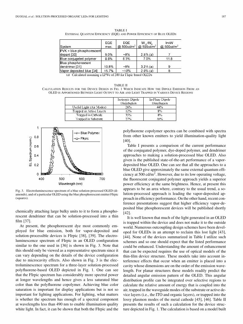
Fig. 3. Electroluminescence spectrum of a blue solution-processed OLED (di-amonds), and of a particular OLED using the blue phosphorescent emitter FIrpic(squares).
chemically attaching large bulky units to it to form a phospho-rescent dendrimer that can be solution-processed into a thinfilm [37].
At present, the phosphorescent dye most commonly em-ployed for blue emission, both for vapor-deposited andsolution-processible devices is FIrpic [38], [39]. The electro-luminescence spectrum of FIrpic in an OLED configurationsimilar to the one used in [36] is shown in Fig. 3. Note thatthis should only be viewed as a representative spectrum since itcan vary depending on the details of the device configurationdue to microcavity effects. Also shown in Fig. 3 is the elec-troluminescence spectrum for a three-layer solution-processedpolyfluorene-based OLED depicted in Fig. 1. One can seethat the FIrpic spectrum has considerably more spectral powerat longer wavelengths and hence gives a less saturated bluecolor than the polyfluorene copolymer. Achieving blue colorsaturation is important for display applications but is not soimportant for lighting applications. For lighting, what mattersis whether the spectrum has enough of a spectral componentat wavelengths less than 490 nm to enable illumination qualitywhite light. In fact, it can be shown that both the FIrpic and the
polyfluorene copolymer spectra can be combined with spectrafrom other known emitters to yield illumination-quality light[40].
Table I presents a comparison of the current performanceof the conjugated polymer, dye-doped polymer, and dendrimerapproaches to making a solution-processed blue OLED. Alsogiven is the published state-of-the-art performance of a vapor-deposited blue OLED. One can see that all the approaches to ablue OLED give approximately the same external quantum effi-ciency at 500 cd/m . However, due to its low operating voltage,the fluorescent conjugated polymer approach yields a superiorpower efficiency at the same brightness. Hence, at present thisappears to be an area where, contrary to the usual trend, a so-lution-processed approach is leading the vapor-deposited ap-proach in efficiency performance. On the other hand, recent con-ference presentations suggest that higher efficiency vapor-de-posited blue phosphorescent devices will be published shortly[42].
It is well known that much of the light generated in an OLEDis trapped within the device and does not make it to the outsideworld. Numerous outcoupling design schemes have been devel-oped for OLEDs in an attempt to reclaim this lost light [43],[44]. None of the devices summarized in Table I utilize suchschemes and so one should expect that the listed performancecould be enhanced. Understanding the amount of enhancementthat can be expected requires the use of optical models of thethin-film device structure. These models take into account in-terference effects that occur when an emitter is placed into acavity whose dimensions are on the order of the emission wave-length. For planar structures these models readily predict thedetailed angular emission pattern of the OLED. This angulardistribution profile can be integrated over selective regions tocalculate the relative amount of energy that is coupled into theair, trapped in the waveguide modes of the substrate or active de-vice layers (i.e., the ITO and organic layers), or trapped into thelossy plasmon modes of the metal cathode [45], [46]. Table IIpresents the results of such a calculation for the device struc-ture depicted in Fig. 1. The calculation is based on a model built

188 JOURNAL OF DISPLAY TECHNOLOGY, VOL. 3, NO. 2, JUNE 2007
by McGehee et al. and requires as input parameters the com-plex index of refraction for each layer along with the orienta-tion of the emitting dipoles of the device relative to the planeof the OLED structure [47]. Dipoles that are oriented perpen-dicular to the plane of the OLED couple most efficiently to theactive layer waveguide modes and cathode plasmon modes ofthe device and least efficiently to the air. Thus, this particularorientation is highly undesirable. Conversely, dipoles that areoriented along the plane of the OLED couple very inefficientlyto the active layer and cathode modes and most efficiently intothe air. Dipoles that have random orientation are intermediatebetween these two extreme cases. Fortuitously, many electroac-tive polymer materials have a linear, rod like structure whichnaturally tends to align along plane of the OLED. Hence de-vices that utilize these materials typically have relatively highoutput coupling to the air. This stands in sharp relief to OLEDwhose emitters are based upon randomly oriented dipoles [48].
Table II shows the results for two separate calculations –one for the dipoles with an isotropic angular distribution andone for the dipoles all aligned along the plane of the interface.The results show that for an isotropic dipole distribution inthis device structure, only 26% of the light makes it out of thedevice as compared to 47% for the in-plane dipole distribution.This indicates that there is more to be gained in improvingoutcoupling efficiency for a device which utilizes a small-mol-ecule dye emitter than for one which utilizes a conjugatedpolymer emitter. The results also indicate that different out-coupling schemes need to be employed for the two differentdipole distributions. For instance, for the isotropic distribution,it is most worthwhile to develop schemes that extract energylost in plasmon modes at the cathode [49] since this is themajor source of loss whereas for the in-plane distribution, suchschemes would be of secondary importance.
The results presented in Table II assume that the emissionzone is located at an optimal position relative to all the otherdielectric layers and interfaces in the device. An additionalinsight of these optical models is that in a standard OLED, theoutput coupling efficiency to the air is a sensitive function ofthe location of the emission zone [48]. Thus, careful adjustmentof the thickness of the device layers is an absolute imperative.In vapor-deposited OLEDs this is achieved via a adjusting thethickness of the various transport layers of the multilayer device[50] whereas for solution-processed devices this is achieved byadjusting the material composition of the layer(s) to achieve anoptimal charge balance and recombination zone position [40].Given the relatively high performance levels achieved by bothsolution-processed devices and by vapor-deposited devices(Table I), both approaches appear to be effective.
Even with careful optimization of the emissive layers, a sig-nificant amount of light is trapped in the substrate for both theisotropic and in-plane dipole distributions and for both casesTable II shows that an approximately 2 enhancement is pos-sible. Since the structure and shape of the substrate can be modi-fied without affecting the performance of the active layers of theOLED, there are numerous possible methods to extract light thatis trapped within substrate modes [51]–[55]. For lighting, wheremaintaining low cost is critical, the scheme of simply applyinga scattering layer on top of the device is quite promising. So far,it has demonstrated a 1.5 enhancement and with optimization
it has the potential to reach the total possible enhancement [56],[57].
IV. NOVEL LOW COST MANUFACTURING
Achieving low cost OLED manufacturing is essential toensure penetration of OLED technology into general lightingapplications. Solution-processed OLEDs are attractive in that itis possible to envision a high throughput “roll-to-roll” printingprocess that can make large area OLEDs at low cost. To date,most effort in developing printable OLEDs has focused ondeveloping inkjet processes to print the active organic layersof an OLED for display applications. However, inkjet printingis not necessarily required for lighting applications where asmall pixel size is not necessary and hence higher throughputprinting processes such as screen-printing, gravure printing, orflexography may be utilized for low cost OLED manufacture.Nevertheless, even with ultra-low cost printing of the organiclayers of an OLED, high device performance typically still re-quires integration with one or more high vacuum process stepsfor electrode formation during device manufacture. This addscomplexity and reduces throughput relative to a pure printingprocess and hence limits the ultimate low cost potential. Itis thus highly desirable to develop an OLED manufacturingprocess that does not require any vacuum process steps.
One approach to eliminating vacuum process steps is to de-velop a printing process for the final electrode layer. Printablemetal technology exists today for metals such as silver and goldbut not for the low work-function metals such as barium or cal-cium which are required for the top cathode of typical down-emitting OLEDs. In addition, available metal printing processestypically require a high temperature bake step which can beproblematic for the underlying OLED materials. However, re-cently it has been shown that OLEDs can be made via printinga top cathode consisting of a gallium/calcium alloy [58]. Theefficiency and lifetime of these devices were on par with con-trol devices made with a vapor-deposited cathode. This suggeststhat the development of a robust, printable cathode for OLEDsmay be possible.
In the following, an alternative approach to eliminatingvacuum processing steps from OLED manufacture is presented(see Fig. 4) [59]. Rather than building a device by sequentiallycoating both the organic layers and a top electrode layer onto aconducting substrate, a portion of the organic layers are coatedonto two separate conducting substrates in parallel and thenthese are laminated together to form the final device. Thislamination approach is inherently compatible with high-speedroll-to-roll manufacturing techniques and is best applied whenboth conducting substrates are mechanically flexible. As anexample, one substrate could be a metal foil while the othercould be a transparent plastic film pre-coated with a transparentconductor. In addition, the lamination approach also providesother advantages over the conventional fabrication method. Forexample, the lamination approach provides a hermetic seal, ifboth substrates possess proper barrier properties and anotherpathway of building multilayer structures that are difficult toachieve with conventional fabrication means.
OLEDs and organic light-emitting electrochemical cells havebeen fabricated via related lamination techniques in the past

DUGGAL et al.: SOLUTION-PROCESSED ORGANIC LEDs FOR LIGHTING 189
Fig. 4. Schematic of a vacuum-free, roll-to-roll lamination process for OLED fabrication.
Fig. 5. Specific lamination process and device configurations for OLEDs fab-ricated with (a) two and (b) three organic semiconductor layers.
[60], [61]. However, for OLEDs, devices with performanceequivalent to what could be achieved with the same organicsemiconductors with conventional processing techniques wereonly demonstrated when multiple high vacuum steps wereintegrated into the lamination process [60]. These high vacuumsteps were required in order to overcome two key issues foundwith “vacuum-less” lamination – the inability to achieve robustelectrical contact between two organic semiconductors at alamination interface and the inability to achieve efficient elec-tron injection into the organic layers from the cathode interface.In the following it is shown that both of these issues can besolved without the integration of high vacuum process steps.
In order to demonstrate that good electrical contact can beachieved between two laminated organic semiconductors, thesimple device structure depicted in Fig. 5(a) was chosen. Heretwo components—an anode side and a cathode side – are lami-nated together with a lamination interface between the hole-in-jection layer (HIL) and the light emitting polymer (LEP) layerof the final device. For our experiments, the conducting sub-strates consisted of 175 m thick films of polyethylene tereph-thalate (PET) pre-coated with 120 nm of ITO for the anode sidecomponent and pre-coated with 100 nm of aluminum for thecathode side component. The HIL material consisted of 65 nmof PEDOT:PSS and the LEP (80 nm) consisted of blue-emit-ting poly(9,9-dioctylfluorenyl-2,7-diyl) end capped with N,N-Bis(4-methylphenyl)-4-aniline (hereafter referred to as PF) ob-tained from American Dye Source, Inc., Quebec, Canada.
The two components were made by spin coating thePEDOT:PSS (anode-side) and PF (cathode-side) onto the ap-propriate conducting substrate and then baking at 110 C for10 minutes to remove residual solvents. These two componentswere then laminated together using a simple roll laminatorpurchased from an office supply store. The web speed through
the laminator was 0.3 m/min and the roll temperature wasset at 150 C, which is above the glass transition temperature(60 C 70 C) of PF. The anode and cathode componentsthat were fed together into the laminator had dimensions of(40 mm 18 mm) and (18 mm 25 mm), respectively, andwere designed to create four active areas of 6 mm 5 mm asdefined by the overlap of the ITO and aluminum. The pressureapplied during lamination was estimated to be about 1.0 10 Pa(15 psi) through calibration with pressure sensitive films. Usingthis lamination process, it was possible to repeatedly fabricateworking OLEDs that lit up uniformly across all active areas.
Fig. 6 shows the optoelectronic performance data for a rep-resentative laminated device. For comparisons, devices with thesame basic layer structure (ITO/PEDOT:PSS/PF/Cathode) weremade using a conventional fabrication process where each de-vice layer is sequentially deposited on top of the other and thefinal cathode is thermally evaporated in vacuum at a base pres-sure of 2 10 Torr. Two types of conventional devices weremade—one with a single Al layer (100 nm) cathode and onewith a Ca/Al bilayer (30 nm/100 nm) cathode—and represen-tative performance data is also shown in Fig. 6. The conven-tionally fabricated device with the single Al cathode layer is di-rectly comparable to the laminated device since they both havethe same nominal device structure (ITO/PEDOT:PSS/PF/Al).
Note that the laminated device has superior optoelectronicperformance as it operates at higher brightness and power ef-ficiency. This clearly suggests that good electrical contact canbe achieved between two organic semiconductors using a lami-nation process. The substantially inferior efficiency of the con-ventional device is most likely due to the damaging effects ofvapor-depositing Al directly onto organic semiconductors ashas been suggested in previous studies [62]. It should be notedthat the laminated devices could easily be pulled apart by handand in such cases separated cleanly at the PEDOT:PSS/PF inter-face. Hence, for these materials, although good electrical con-tact could be achieved during lamination, the mechanical adhe-sion achieved was relatively weak.
As shown in Fig. 6, the conventionally fabricated device witha Ca–Al bilayer cathode still has superior performance relativeto the laminated Al cathode device. This is expected since Cahas a lower work function than Al and hence has a lower bar-rier for electron injection into the lowest unoccupied molecularorbitals (LUMO’s) of the PF. Thus for the Ca–Al cathode de-vice one observes lower device operating voltage and aincrease in power efficiency due to better electron injection andpresumably better charge balance. In fact, all high performance

190 JOURNAL OF DISPLAY TECHNOLOGY, VOL. 3, NO. 2, JUNE 2007
Fig. 6. (a) Brightness versus bias voltage and (b) power efficiency versus current density of OLEDs made via lamination (solid symbols) or conventional sequentialdeposition with cathode evaporation (open symbols). The associated device structures are ITO/HIL/LEP/Al (triangles), ITO/HIL/LEP/Ca/Al (open squares), andITO/HIL/LEP/EIL/Al (solid squares).
OLEDs utilize either a low work-function cathode or an n-dopedorganic semiconductor electron-injection layer (EIL) adjacentto the device cathode to enhance electron injection [61]. Todate, these approaches have always involved vacuum depositionduring OLED fabrication. In the following, it is shown that it ispossible to create a solution-processible n-doped EIL and inte-grate this into a lamination process.
Chemical reducing or n-doping an organic semiconductor tocreate an EIL is equivalent to adding electron population to thematerial LUMO levels. This facilitates electron injection intothe EIL from a high work function electrode such as Al. Ourstrategy for EIL design was to chemically reduce the same basePF material that is utilized for the LEP as this would enableefficient injection from the EIL to the LEP since the LUMOlevels would be at approximately the same energy. The reduc-tion was accomplished in solution by adding potassium metalto the PF. Specifically, EIL solutions were made by combining10 mg of PF in 10 mL of ethyleneglycol dimethylether (DME)with 5 mg of potassium metal and then stirring at ambient tem-perature after subjecting the solutions to three freeze/degas/thawcycles. During this procedure, the colorless the solution changedto dark blue.
The n-doped EIL solution (PF:K) was utilized as an EIL tocreate a laminated OLED with the device structure and lamina-tion interface depicted in Fig. 5(b). Note that it would be difficultto make this particular device structure using a conventional se-quential solution-based deposition process because any solventused to deposit the EIL onto the LEP would likely wash outthe underlying LEP layer. This results from the design strategyof using the same base PF material for both the EIL and LEPlayers. In order to fabricate this device structure via lamina-tion, the cathode-side component was formed by spin-coatinga 20-nm PF:K layer onto the conducting substrate and baking at110 C while the anode-side component was fabricated as be-fore except that an 80-nm PF layer was spin-coated on top of thePEDOT:PSS layer. The two components were then laminatedtogether as described previously to form functional devices. Itshould be noted that the PF:K solution is highly reactive to airand water and thus, for these experiments, the preparation of thecathode-side component and the final lamination step were con-ducted in an argon atmosphere with oxygen and moisture levelsbelow 5 ppm.
Fig. 7. A laminated OLED consisting of two rows of OLED elements whereeach element has a dimension of 1/2” by 1/2”.
The laminated devices again lit up uniformly across allactive areas and also exhibited relatively weak mechanicaladhesion. The optoelectronic performance of a representativedevice is depicted in Fig. 6. Note that it exhibits dramaticallylowered operating voltage and enhanced efficiency relativeto the representative laminated device without an EIL. Rel-ative to the conventionally processed Ca/Al cathode device,it exhibits slightly higher voltage Fig. 6(a) but equivalentpower efficiency for a given current density Fig. 6(b). Thissuggests that the laminated device has slightly worse electroninjection than the conventional device but that this is offset bybetter charge balance. It should be noted that the performanceof the Ca/Al cathode device represents approximately thehighest power-efficiency OLED that we have achieved withconventional processing with this particular set of organicsemiconductor materials. The fact that we can replicate thisefficiency with lamination shows that it is possible to design avacuum-free OLED fabrication process without compromisingdevice performance. The lifetime of these laminated OLEDs iscurrently limited by the fact that the PET substrate used in thiswork does not have proper barrier properties.
The vacuum-free lamination technique clearly has the po-tential to enable ultralow cost OLED manufacturing. However,in order to be relevant for lighting applications, the techniquemust be scalable to large area devices. The key impediment toachieving this with the process described above is the poor in-terfacial adhesion between the laminated organic layers. It is inlarge part possible to design around this weak interface througha more sophisticated multilayer lamination process design. Asan example, Fig. 7 shows a green-emitting OLED that was madewith a more sophisticated lamination process. It utilizes a scal-able monolithic series-connected architecture [7] relevant for

DUGGAL et al.: SOLUTION-PROCESSED ORGANIC LEDs FOR LIGHTING 191
lighting and consists of two rows of emitting elements whereeach element has a dimension of 1/2” by 1/2”. The device is morerobust mechanically than the devices described earlier in that itcould be flexed repeatedly without failure. Nevertheless, morecomplex lamination processes are less generally applicable andso in the future it would be highly desirable to develop materialsolutions that can improve the inherent adhesion at the lamina-tion interface.
V. CONCLUSION
The design paradigm for solution-processible OLED tech-nology development has focused on adding as much function-ality as possible into the active organic materials and then touse these materials in device structures with as few active layersas possible. This is in contrast to vapor-deposited OLED tech-nology, which has progressed by exploiting many-layer devicedesigns with simpler small-molecule materials. In general, dueto the faster research turnaround time, the vapor-deposited tech-nology has been the first to demonstrate each new device perfor-mance milestone but so far the solution-processed technologyhas always been able to follow. For lighting applications, the so-lution-processed technology is attractive because it has the po-tential for providing the lowest possible OLED manufacturingcost.
In order to achieve high efficiency, illumination-qualitywhite light, it is important to focus effort on developing lowcost-structure OLEDs that are capable of emitting blue lightwith high efficiency. The blue device results described in thispaper show that at present the highest efficiency devices at alighting relevant brightness utilize singlet emission from solu-tion-processed conjugated polymers. However, achieving therequired 30 W W efficiency required for lighting willrequire device designs and materials that can utilize triplet ex-citons and optimal outcoupling strategies. Achieving the lowestpossible manufacturing cost will require the utilization of highthroughput printing processes that do not require integrationwith high vacuum process steps. Our results indicate that alamination process that fits this requirement can be utilized forOLED manufacture without paying a price in performance.Scaling this process up for large area lighting devices willlikely require the development of new solution-processed ma-terials specifically optimized to improve the inherent adhesionbetween the organic layers at the lamination interface. As moreresearch effort focuses on these needs, there is good reasonto be optimistic that solution-processed OLEDs will be ableto meet the cost and performance requirements for generallighting.
REFERENCES
[1] R. H. Friend, R. W. Gymer, A. B. Holmes, J. H. Burroughes, R. N.Marks, C. Taliani, D. D. C. Bradley, D. A. Dos Santos, J. L. Bredas, M.Logdlund, and W. R. Salaneck, “Electroluminescence in conjugatedpolymers,” Nature, vol. 397, pp. 121–128, Jan. 1999.
[2] S. R. Forrest, “Active optoelectronics using thin-film organic semicon-ductors,” IEEE J. Sel. Topics Quantum Electron., vol. 6, no. 6, pp.1072–1083, Nov./Dec. 2000.
[3] A. Bergh, G. Craford, A. Duggal, and R. Haitz, “The promise and chal-lenge of solid-state lighting,” Physics Today, vol. 54, pp. 42–47, Dec.2001.
[4] A. R. Duggal, “Organic electroluminescent devices for solid statelighting,” in Org. Electrolum., Z. H. Kafafi, Ed. Boca Raton, FL:Taylor & Francis, 2005, pp. 437–466.
[5] A. R. Duggal, C. M. Heller, D. F. Foust, and J. J. Shiang, “Organiclight-emitting devices for illumination-quality white light,” Appl. Phys.Lett., vol. 80, pp. 3470–3472, May 2002.
[6] B. W. D’Andrade and S. R. Forrest, “White organic light-emitting de-vices for solid-state lighting,” Adv. Mat., vol. 16, pp. 1585–1595, Sep.2004.
[7] A. R. Duggal, D. F. Foust, W. F. Nealon, and C. M. Heller, “Fault-tol-erant, scalable organic light-emitting device architecture,” Appl. Phys.Lett., vol. 82, pp. 2580–2582, Apr. 2003.
[8] T. Matsumoto, T. Nakada, J. Endo, K. Mori, N. Kawamura, A. Yokoi,and J. Kido, “Multiphoton organic EL device having charge generationlayer,” in Soc. Inf. Display Int. Symp. Dig. Tech. Papers , 2003, vol. 34,pp. 979–981.
[9] L. S. Liao, K. P. Klubek, and C. W. Tang, “High-efficiency tandemorganic light-emitting diodes,” Appl. Phys. Lett., vol. 84, pp. 167–169,, Jan. 2004.
[10] A. Chwang, M. A. Rothman, S. Y. Mao, R. H. Hewitt, M. S. Weaver,J. A. Silvernail, K. Rajan, M. Hack, J. J. Brown, X. Chu, L. Moro, T.Krajewski, and N. Rutherford, “Thin film encapsulated flexible organicelectroluminescent displays,” Appl. Phys. Lett., vol. 83, pp. 413–415,Jul. 2003.
[11] M. Yan, T. W. Kim, A. G. Erlat, M. Pellow, D. F. Foust, J. Liu, M.Schaepkens, C. M. Heller, P. A. McConnelee, T. P. Feist, and A. R.Duggal, “A transparent, high barrier, and high heat substrate for organicelectronics,” Proc. IEEE, vol. 93, pp. 1468–1477, Aug. 2005.
[12] C. W. Tang and S. A. VanSlyke, “Organic electroluminescent diodes,”Appl. Phys. Lett., vol. 51, pp. 913–915, Sep. 1987.
[13] C. W. Tang, S. A. VanSlyke, and C. H. Chen, “Electroluminescence ofdoped organic thin films,” J. Appl. Phys., vol. 65, pp. 3610–3616, May1989.
[14] M. A. Baldo, D. F. O’Brien, Y. You, A. Shoustikov, S. Sibley, M. E.Thompson, and S. R. Forrest, “Highly efficient phosphorescent emis-sion from organic electroluminescent devices,” Nature, vol. 395, pp.151–154, Sep. 1998.
[15] J. Endo, T. Matsumoto, and J. Kido, “Organic electroluminescent de-viceswith a vacuum-deposited Lewis-acid-doped hole-injecting layer,”Jpn. J. Appl. Phys., vol. 41, pp. L358–L360, Mar. 2002.
[16] X. Zhou, M. Pfeiffer, J. Blochwitz, A. Werner, A. Nollau, T. Fritz,and K. Leo, “Very-low-operating-voltage organic light-emitting diodesusing a p-doped amorphous hole injection layer,” Appl. Phys. Lett., vol.78, pp. 410–412, Jan. 2001.
[17] G. Parthasarathy, C. Shen, A. Kahn, and S. R. Forrest, “Lithium dopingof semiconducting organic charge transport materials,” J. Appl. Phys.,vol. 89, pp. 4986–4992, May 2001.
[18] G. He, M. Pfeiffer, K. Leo, M. Hofmann, J. Birnstock, R. Pudzich, andJ. Salbeck, “High-efficiency and low-voltage p- i-n electrophosphores-cent organic light-emitting diodes with double-emission layers,” Appl.Phys. Lett., vol. 85, pp. 3911–3913, Oct. 2004.
[19] R. H. Partridge, “Radiation sources,” U.S. Patent 3 995 299, Nov. 30,1976.
[20] R. H. Partridge, “Electroluminescence from polyvinylcarbazole films:Pt. 1: Cabazole cations,” Polymer, vol. 24, pp. 733–738, Jun. 1983.
[21] R.H. Partridge, “Polyvinylcarbazole films containing antimony pen-tachloride,” Polymer, vol. 24, pp. 739–747, Jun. 1983.
[22] R.H. Partridge, “Electroluminescent devices,” Polymer, vol. 24, pp.748–752, Jun. 1983.
[23] R.H. Partridge, “Electroluminescence using higher work function cath-odes,” , vol. 24, pp. 755–762, Jun. 1983.
[24] J. Kido, H. Shionoya, and K. Nagai, “Single-layer white light-emit-ting organic electroluminescent devices based on dye-dispersed poly(N-vinylcarbazole,” Appl. Phys. Lett, vol. 67, pp. 2281–2283, Oct. 1995.
[25] A. Nakamura, T. Tada, M. Mizukami, and S. Yagyu, “Efficientelectrophosphorescent polymer light-emitting devices using a Cs/Alcathode,” Appl. Phys. Lett., vol. 84, pp. 130–132, Jan. 2004.
[26] S. A. Choulis, M. K. Mathai, V.-E. Choong, and F. So, “Highly efficientorganic electroluminescent device with modified cathode,” Appl. Phys.Lett, vol. 88, pp. 203502-1–203502-3, May 2006.
[27] J. H. Burroughes, D. D. C. Bradley, A. R. Brown, R. N. Marks, K.Mackay, R. H. Friend, P. L. Burns, and A. B. Holmes, “Light-emittingdiodes based on conjugated polymers,” Nature, vol. 347, pp. 539–541,Oct. 1990.
[28] D. Braun and A. J. Heeger, “Visible light emission from semicon-ducting polymer diodes,” Appl. Phys. Lett., vol. 58, p. 1982, May 1991.
[29] Y. Yang and A. J. Heeger, “Polyaniline as a transparent electrode forpolymer light-emitting diodes: Lower operating voltage and higher ef-ficiency,” Appl. Phys. Lett., vol. 64, pp. 1245–1247, Mar. 1994.

192 JOURNAL OF DISPLAY TECHNOLOGY, VOL. 3, NO. 2, JUNE 2007
[30] S. A. Carter, M. Angelopoulos, S. Karg, P. J. Brock, and J. C. Scott,“Polymeric anodes for improved polymer light-emitting diode perfor-mance,” Appl. Phys. Lett., vol. 70, pp. 2067–2069, Apr. 1997.
[31] W. Wu, M. Inbasekaran, M. Hudack, D. Welsh, W. Yu, Y. Cheng,C. Wang, S. Kram, M. Tacey, M. Bernius, R. Fletcher, K. Kiszka, S.Munger, and J. O’Brien, “Recent development of polyfluorene-basedRGB materials for light emitting diodes,” Microelectron. J., vol. 35, pp.343–348, 2004.
[32] H. F. Ivey, “Color and efficiency of luminescent light sources,” J. Opt.Soc. Am., vol. 53, pp. 1185–1198, 1963.
[33] W. A. Thornton, “ Luminosity and color-rendering capability of whitelight,” J. Opt. Soc. Amer., , vol. 61, pp. 1155–1163, Sep. 1971.
[34] A. Zukauskas, R. Vaicekauskas, F. Ivanauskas, R. Gaska, and M. S.Shur, “Optimization of white polychromatic semiconductor lamps,”Appl. Phys. Lett., vol. 80, pp. 234–236, Jan. 2002.
[35] J.-S. Kim, R. H. Friend, I. Grizzi, and J. H. Burroughs, “Spin-cast thinsemiconducting polymer interlayer for improving device efficiency ofpolymer light-emitting diodes,” Appl. Phys. Lett., vol. 87, pp. 023506-1–1023506-3, Jul. 2005.
[36] X. H. Yang, F. Jaiser, S. Klinger, and D. Neher, “Blue polymer elec-trophosphorescent devices with differentelectron-transporting oxadia-zoles,” Appl. Phys. Lett., vol. 88, pp. 021107-1–021107-3, Jan. 2006.
[37] S.-C. Lo, G. J. Richards, J. P. J. Markham, E. B. Namdas, S. Sharma,P. L. Burn, and I. D. W. Samuel, “A light-blue phosphorescentdendrimer for efficient solution-processed light-emitting diodes,” Adv.Funct. Mat., vol. 15, pp. 1451–1458, Sep. 2005.
[38] R. J. Holmes, S. R. Forrest, Y.-J. Tung, R. C. Kwong, J. J. Brown, S.Garon, and M. E. Thompson, “Blue organic electrophosphorescenceusing exothermic host-guest energy transfer,” Appl. Phys. Lett., vol. 82,pp. 2422–2224, Apr. 2003.
[39] T. Sajoto, P. I. Djurovich, A. Tamayo, M. Yousufuddin, R. Bau, andM. E. Thompson, “Blue and Near-UV Phosphorescence from IridiumComplexes with Cyclometalated Pyrazolyl or N-Heterocyclic CarbeneLigands, ,” Inorg. Chem., vol. 44, pp. 7992–8003, Oct. 2005.
[40] J. J. Shiang and A. R. Duggal, Unpublished results.[41] M.-H. Tsai, H.-W. Lin, H.-C. Su, T.-H. Ke, C.-C. Wu, F.-C. Fang, Y.-L.
Liao, K.-T. Wong, and C.-I. Wu, “Highly efficient organic blue elec-trophosphorescent devices based on 3,6-Bis(triphenylsilyl)carbazole asthe host material,” Adv. Mat., vol. 18, pp. 1216–1220, May 2006.
[42] R. Service, “Organic LEDS look forward to a bright,white future,” Sci-ence, vol. 310, pp. 1762–1763, Dec. 2005.
[43] J.-S. Kim, P. K. H. Ho, N. C. Greenham, and R. H. Friend, “Electro-luminescence emission pattern of organic light-emitting diodes: Impli-cations for device efficiency calculations,” J. Appl. Phys., vol. 88, pp.1073–1081, Jul. 2000.
[44] M. H. Lu and J. C. Sturm, “Optimization of external coupling and lightemission in organic light-emitting devices: Modeling and experiment,”J. Appl. Phys., vol. 91, pp. 595–604, Jan. 2002.
[45] W. L. Barnes, “Electromagnetic crystals for surface plasmon polaritonsand the extraction of light from emissive devices,” J. Lightwave Tech.,vol. 17, pp. 2170–2182, Nov. 1999.
[46] R. R. Chance, A. Prock, and R. Silbey, Adv. in Chem. Phys., vol. 37,pp. 1–65, 1978.
[47] J. M. Ziebarth and M. D. McGehee, “A theoretical and experimentalinvestigation of light extraction from polymer light-emitting diodes,”J. Appl. Phys., vol. 97, pp. 064502-1, 064502-7, Mar. 2005.
[48] C. M. Ramsdale and N. C. Greenham, “The optical constants of emitterand electrode materials in polymer light-emitting diodes,” J. Phys. D:Appl. Phys., vol. 36, pp. L29–L34, Jan. 2003.
[49] J. M. Lupton, B. J. Matterson, I. D. W. Samuel, M. J. Dory, and W.L. Barnes, “Bragg scattering from periodically microstructured lightemitting diodes,” Appl. Phys. Lett., vol. 77, pp. 3340–3342, Nov. 2000.
[50] V. Bulovic, V. B. Khalifin, G. Gu, P. E. Burrows, D. Z. Garbuzov,and S. R. Forrest, “Weak microcavity effects in organic light-emittingdevices,” Phys. Rev. B., vol. 58, pp. 3730–3740, Aug. 1998.
[51] S. Möller and S. F. Forrest, “Improved light out-coupling in organiclight emitting diodes employing ordered microlens arrays,” J. Appl.Phys., vol. 91, pp. 3324–3327, Mar. 2002.
[52] G. Gu, , D. Z. Garbuzov, P. E. Burrows, S. Venkatesh, S. R. Forrest,and M. E Thompson, “High-external-quantum-efficiency organic light-emitting devices,” Opt. Lett., vol. 22, pp. 396–398, Mar. 1997.
[53] C. F. Madigan, M. H. Lu, and J. C. Sturn, “Improvement of output cou-pling efficiency of organic light-emitting diodes by backside substratemodification,” Appl. Phys. Lett., vol. 76, pp. 1650–1652, Mar.. 2000.
[54] T. Tatsui, M. Yahiro, H. Yokogawa, K. Kawano, and M. Yokoyama,“Doubling coupling-out efficiency in organic light emitting devicesusing a thin silica aerogel layer,” Adv. Mat., vol. , pp. 1149–1152, Aug.2001.
[55] T. Yamasaki, K. Sumioka, and T. Tsutsui, “Organic light-emitting de-vice with an ordered monolayer of silica microspheres as a scatteringmedium,” Appl. Phys. Lett., vol. 76, pp. 1243–1245, Mar. 2000.
[56] J. J. Shiang and A. R. Duggal, “Application of radiative transport theoryto light extraction from organic light emitting diodes,” J. Appl. Phys.,vol. 95, pp. 2880–2888, Mar. 2004.
[57] J. J. Shiang, T. J. Faircloth, and A. R. Duggal, “Experimental demon-stration of increased organic light emitting device output via volumetriclight scattering,” J. Appl. Phys., vol. 95, pp. 2889–2895, Mar. 2004.
[58] N. Itoh, T. Akai, H. Maeda, and D. Aoki, “Development of novel pastecathode for all print fabricating OLED devices,” in SID Symp. Dig. ofTech. Papers, Jun. 2006, vol. 37, pp. 1559–1562.
[59] J. Liu, L. N. Lewis, T. J. Faircloth, and A. R. Duggal, “High perfor-mance organic light-emitting diodes fabricated via a vacuum-free lam-ination process,” Appl. Phys. Lett., vol. 88, pp. 223509-1–223509-3,Jun. 2006.
[60] T. F. Guo, S. Pyo, S. C. Chang, and Y. Yang, “High performancepolymer light-emitting diodes fabricated by a low temperature lami-nation process,” Adv. Funct. Mater., vol. 11, pp. 339–343, Oct. 2001.
[61] T. W. Lee, J. Zaumseil, Z. N. Bao, J. W. P. Hsu, and J. A. Rogers,“Organic light-emitting diodes formed by soft contact lamination,” inProc. Natl. Acad. Sci., USA, Jan. 2004, vol. 101, pp. 429–433.
[62] J. Liu, A. R. Duggal, J. J. Shiang, and C. M. Heller, “Efficient bottomcathodes for organic light-emitting devices,” Appl. Phys. Lett., vol. 85,pp. 837–839, Aug. 2004.
Anil R. Duggal received the A.B. degree in chemistry from Princeton Univer-sity, Princeton, NJ, in 1987, and the Ph.D. degree in physical chemistry fromthe Massachusetts Institute of Technology, Cambridge, in 1992.
In 1992, he joined General Electric (GE) Global Research, Niskayuna, NY,and has been working on various aspects of optoelectronics. He is currentlyleading the organic electronics advanced technology program at GE.
Christian M. Heller received the M.S. degree in technical physics from theTechnical University Graz, Graz, Austria, in 1992.
He has been working on OLEDs and packaging issues first with LosAlamos National Laboratory, Los Alamos, NM, then with eMagin Corporation,Hopewell Junction, NY, and since 2001, he has been with General ElectricGlobal Research, Niskayuna, NY.
Joseph J. Shiang received the B.S. degree in chemistry from the CaliforniaInstitute of Technology in 1989, and the Ph.D. degree in physical chemistryfrom the University of California, Berkeley, in 1994.
Since 1999, he has been with General Electric Global Research, Niskayuna,NY, and has been working on organic electronic devices.
Jie Liu received the B.S. degree in chemical engineering from Dalian Universityof Technology, China, in 1993, the M.S. degree in chemistry from the Institute ofChemistry, Chinese Academy of Science, Beijing, China, in 1996, and the Ph.D.degree in material sciences and engineering from the University of California,Los Angeles, in 2001.
In 2002 he joined General Electric Global Research, Niskayuna, NY, and hasbeen working on organic electronic devices.
Larry Lewis received the B.S. degree in chemistry from the State Universityof New York Stony Brook in 1976, and the Ph.D. degree in inorganic chemistryfrom Indiana University, Bloomington, in 1980.
In 1982 he joined General Electric Global Research, Niskayuna, NY.In 2000, Dr. Lewis was awarded the Coolidge Fellowship, GE’s highest tech-
nical award.