Solar cell demand for bifacial and singulated-cell module ... cell... · 60-cell module with a size...
13
48 www.pv-tech.org Market Watch Cell Processing Fab & Facilities Thin Film Materials PV Modules Introduction The first appearance of a shingled solar cell interconnection pattern (see Fig. 1) dates back to 1956 with a US patent filed by Dickson [1] for Hoffman Electronics Corporation, which is just two years after the first publication of a silicon solar cell by Chapin et al. [2]. In the years that followed, further patents were filed containing concepts of shingling solar cells serving various module designs and applications – for example, Nielsen [3] for Nokia Bell Labs, Myer [4] for Hughes Aircraft Company, Baron [5] for Trw Inc, Gochermann and Soll [6] for Daimler- Benz Aerospace AG, Yang et al. [7] for Silevo LLC, and the most recent patent applications by Morad et al. [8–10] for SunPower Corporation in 2016. Besides the patents, there are a number of items in the literature that have been devoted to this topic in the last few years, with publications by Zhao et al. [11], Glunz et al. [12] and Beaucarne [13]. Recently, the first widely available commercial shingled module was introduced by SunPower [14] as their top-of-the-line product; according to the data sheet, these modules feature a backsheet and are therefore not bifacial. The idea of singulated solar cells interconnected by a shingling design is therefore by no means new. The early publications of shingling approaches were mostly motivated by particular design requirements, such as modules that were curved, triangular [4] or dome shaped [6]. Later publications started to make use of the potential for achieving Solar cell demand for bifacial and singulated-cell module architectures Nico Wöhrle, Elmar Lohmüller, Max Mittag, Anamaria Moldovan, Puzant Baliozian, Tobias Fellmeth, Karin Krauss, Achim Kraft & Ralf Preu, Fraunhofer Institute for Solar Energy Systems ISE, Freiburg, Germany ABSTRACT The pursuit of achieving higher power output of silicon-based PV modules demands creative improvements in module design in order to reduce geometrical, optical and electrical cell-to-module (CTM) losses. A suitable method, which has been known since Dickson’s patent in 1956 (but has been mostly under the radar of the manufacturing industry), is the shingling of singulated solar cell stripes. This technology offers three advantages in comparison to modules with standard-sized solar cells. First, blank cell spacing in the module is minimized, thus increasing the power-generating area per module area. Second, the active cell area is busbar-less, which leads to reduced shading losses. Third, because of the smaller area of the solar cell stripes, the generated current per cell is less, which results in a reduction in the overall series resistance of the cell interconnection within the module. To boost the power output of such a shingled module even further, the introduction of bifacial properties is suggested. To make this bifacial shingled module technology visible on the industry’s radar, a practical concept is essential; this paper presents, step by step, Fraunhofer ISE’s approach for a bifacial shingled module. Suitable bifacial cell concepts – such as passivated emitter and rear (PERC), passivated emitter, rear totally diffused (PERT), and passivated emitter, rear locally diffused (PERL) – are briefly introduced. The PERL cells are based on the PassDop approach, in which the rear-side passivation layer stack also acts as a doping source during local laser doping. Furthermore, next-generation bifacial cell concepts based on selective and/or passivated contacts, such as in the already established silicon heterojunction technology (SHJ) and the tunnel oxide passivated contact (TOPCon) approaches, developed at Fraunhofer ISE, are presented. Laser-assisted cutting as the singulation technology for realizing the cell stripes, and the challenge of charge-carrier recombination at the cutting edges, are discussed. A bifacial simulation model is presented for the singulated shingle solar cells, covering the question of the impact of different recombination factors, bifacial gains and optimizations of the cell layout. Finally, the module assembly, as well as a detailed calculation of module output power and a comparison with standard module layouts, is presented. This comparison emphasizes the advantages offered by bifacial shingled modules, with the potential to achieve a module power of 400W with a power density of 240W/m 2 and beyond, for irradiance intensities of 1,000W/m 2 and 100W/m 2 from the front and rear sides respectively. Figure 1. First published illustration of the shingling scheme for monofacial silicon solar cells, taken from Dickson’s patent [1] (the descriptive labels in the original image have been removed for reasons of clarity).
-
Upload
nguyenhanh -
Category
Documents
-
view
215 -
download
0
Transcript of Solar cell demand for bifacial and singulated-cell module ... cell... · 60-cell module with a size...

48 w w w.pv- tech.org
Market Watch
Cell Processing
Fab & Facilities
Thin Film
Materials
PV Modules
IntroductionThe first appearance of a shingled solar cell interconnection pattern (see Fig. 1) dates back to 1956 with a US patent filed by Dickson [1] for Hoffman Electronics Corporation, which is just two years after the first publication of a silicon solar cell by Chapin et al. [2]. In the years that followed, further patents were filed containing concepts of shingling solar cells serving various module de s ig ns and appl ic at ions – for example, Nielsen [3] for Nokia Bell Labs, Myer [4] for Hughes Aircraft Company, Baron [5] for Trw Inc, Gochermann and Soll [6] for Daimler-Benz Aerospace AG, Yang et al. [7] for Silevo LLC, and the most recent patent applications by Morad et al. [8–10] for SunPower Corporation in 2016. Besides the patents, there are a number of items in the literature that have been devoted to this topic in the last few years, with publications by Zhao et al. [11], Glunz et al. [12] and Beaucarne [13]. Recently, the first
widely available commercial shingled module was introduced by SunPower [14] as their top-of-the-line product; according to the data sheet, these modules feature a backsheet and are therefore not bifacial.
The idea of singulated solar cells interconnected by a shingling design
is therefore by no means new. The e a r ly publ ic at ion s of sh i ng l i ng approaches were mostly motivated by particular design requirements, such as modules that were curved, triangular [4] or dome shaped [6]. Later publications started to make use of the potentia l for achieving
Solar cell demand for bifacial and singulated-cell module architecturesNico Wöhrle, Elmar Lohmüller, Max Mittag, Anamaria Moldovan, Puzant Baliozian, Tobias Fellmeth, Karin Krauss, Achim Kraft & Ralf Preu, Fraunhofer Institute for Solar Energy Systems ISE, Freiburg, Germany
ABSTRACTThe pursuit of achieving higher power output of silicon-based PV modules demands creative improvements in module design in order to reduce geometrical, optical and electrical cell-to-module (CTM) losses. A suitable method, which has been known since Dickson’s patent in 1956 (but has been mostly under the radar of the manufacturing industry), is the shingling of singulated solar cell stripes. This technology offers three advantages in comparison to modules with standard-sized solar cells. First, blank cell spacing in the module is minimized, thus increasing the power-generating area per module area. Second, the active cell area is busbar-less, which leads to reduced shading losses. Third, because of the smaller area of the solar cell stripes, the generated current per cell is less, which results in a reduction in the overall series resistance of the cell interconnection within the module. To boost the power output of such a shingled module even further, the introduction of bifacial properties is suggested. To make this bifacial shingled module technology visible on the industry’s radar, a practical concept is essential; this paper presents, step by step, Fraunhofer ISE’s approach for a bifacial shingled module. Suitable bifacial cell concepts – such as passivated emitter and rear (PERC), passivated emitter, rear totally diffused (PERT), and passivated emitter, rear locally diffused (PERL) – are briefly introduced. The PERL cells are based on the PassDop approach, in which the rear-side passivation layer stack also acts as a doping source during local laser doping. Furthermore, next-generation bifacial cell concepts based on selective and/or passivated contacts, such as in the already established silicon heterojunction technology (SHJ) and the tunnel oxide passivated contact (TOPCon) approaches, developed at Fraunhofer ISE, are presented. Laser-assisted cutting as the singulation technology for realizing the cell stripes, and the challenge of charge-carrier recombination at the cutting edges, are discussed. A bifacial simulation model is presented for the singulated shingle solar cells, covering the question of the impact of different recombination factors, bifacial gains and optimizations of the cell layout. Finally, the module assembly, as well as a detailed calculation of module output power and a comparison with standard module layouts, is presented. This comparison emphasizes the advantages offered by bifacial shingled modules, with the potential to achieve a module power of 400W with a power density of 240W/m2 and beyond, for irradiance intensities of 1,000W/m2
and 100W/m2 from the front and rear sides respectively.
Figure 1. First published illustration of the shingling scheme for monofacial silicon solar cells, taken from Dickson’s patent [1] (the descriptive labels in the original image have been removed for reasons of clarity).

Photovoltaics International 49
Cell Processing
higher module power densities with this technique than with standard-module cel l interconnect ion, for example in the limited available space on the vehicle for the ‘World Solar Challenge’ in 1996 [11]. Consequently, a few large module manufacturers [7,14] seem to have rediscovered the potentia l of shingl ing technology to reduce cel l-to-modu le (CTM) losses. The International Technology Roadmap for Photovoltaic (ITRPV) 2017 projects a world market share of 7% for shingled interconnection technology by 2027 [15].
“The opportunity is at hand for combining bifacial solar cell technology with shingle
cell module technology.”A not her l i ne of tech nolog ica l
e vo lut ion spre ad i n g i n t he PV industry is the concept of bifacially i l luminated solar cel ls, which has been extensively covered in a recent article by Kopecek and Libal [16]. As the demand for modules with h igh power densit y i s la rge, the opportunity is at hand for combining bifacial solar cel l technology with shingle cell module technology, with bifacial cells profiting from additional
light coming from the rear side. The busbars on the front and rear sides for the shingle cells are covered by an active area from the adjacent cells, leading to a virtually busbar-free cell string.
The approach for such a bifacial shingle module is presented in three stages. First , el ig ible bi facia l cel l concepts – includ ing passivated e m i t t e r a n d r e a r (PE RC [17]) , pa ss iv ated em it ter, rea r tot a l ly diffused (PERT [18]), and passivated emitter, rear locally diffused (PERL [19]) – wil l be discussed. For this study, the PERL concept is based on
the PassDop approach [20–22], in which the rear-side passivation layer stack – i.e. the layer stack consisting of a lu m i n iu m ox ide (A lO x) a nd boron-doped silicon nitride (SiNx:B) – also serves as a doping source for loca l laser doping. Furthermore, cell concepts with selective and/or passivated contacts that are based on silicon heterojunction (SHJ [23]) or hybr id PERC st ruct ures w ith tunnel ox ide passivated contacts (TOPCon [24]) on the rear side will be discussed. Second, physically and technically relevant challenges for the transition from standard cel ls
Figure 3. Schematic cross sections of seven different silicon solar cell types with homogeneous emitter. (a) Aluminium back-surface field (Al-BSF) cell. (b) Monofacial PERC with local rear-side contacts. (c) Bifacial PERC with finger grid on the rear side. (d) Bifacial PERT concept with full-area rear-side BSF. (e) Bifacial pPassDop concept with local laser-boron-doped BSF. (f) Silicon heterojunction (SHJ) cell with doped amorphous silicon emitter and a transparent conducting oxide (TCO) as anti-reflection layer. (g) Bifacial TOPCon cell with passivated rear-side contacts (the bifacial rear side shown is only a concept at the moment).
(a) Al-BSF (b) PERC (c) biPERC (d) biPERT
(e) pPassDop (f ) SHJ (g) TOPCon
Figure 2. Schematic of the different process steps in the fabrication of shingle modules, starting from bifacial cells on a standard-sized wafer with an edge length of 156mm. (a) Six shingle solar cells are placed on the large-area wafer. The cell concept is modular; silicon heterojunction (SHJ), TOPCon and PERC examples are shown here. (b) The individual shingle cells are singulated into cell stripes. (c) A magnified single shingle cell. (d) Cell stripes are shingled onto each other to form a string.
(a) (b) (c) (d)

50 w w w.pv- tech.org
Cell Processing
to str ipe cel ls wi l l be addressed, i nc lud i ng a d i s c u s s ion of e dge recombination effects with a suitable full-cell simulation model realized with the Quokka3 tool [25]. Third, module integration strategies and CTM-loss calculations are provided.
A s a n a m e c o n v e n t i o n , t h e t e r m ‘o u t p u t p o w e r d e n s i t y ’ Pout (mW/cm2) wil l always be used i n s t e a d o f ‘e n e r g y c o n v e r s i o n efficiency’ η (%) for measurement data referring to bifacial illumination, as that unit is less ambiguous. The scale chosen is such that, with a monofacial i r r ad i a t i o n o f 1 , 0 0 0W/m 2 , t h e respective numerical values for Pout and η are identical.
ApproachTo achieve a module output power Pmodule of 400W with power densities of 240W/m2 and beyond for a standard 60-cell module with a size of 1.68m × 1.00m (irradiation intensities of 1,000W/m2 and 100W/m2 from the front and rear sides respectively), the approach proposed here is to apply shingling technology in order to use the module area as efficiently as possible. By shingling the solar cells, three CTM-related types of loss are minimized, namely 1) losses due to inactive module area; 2) shading losses due to busbar contacts; and 3) series resistance losses due to cell interconnection. To also benefit from the additional rear-side illumination from bifacial solar cell architectures, the proposed shingle solar cell and module technology is also bifacial in nature. The authors foresee a large potential for this bifacial shingling approach in cases where the ‘old idea’ of shingled modules can be merged with state-of-the art bifacial solar cell concepts.
To raise interest with regard to industrial mass production, standard-s i z e d s o l a r ce l l m a nu f ac t u r i n g s e q u e n c e s , w i t h o n l y m i n o r adaptations, should be utilized for the manufacturing of shingle solar cells. Thus, the most obvious industrial solar cell concept to be used is the bifacial passivated emitter and rear cell (biPERC) technology, utilizing p-type Czochralsk i-grown si l icon (Cz-Si) wa fers . Fig . 2 i l lust rates four different typical stages of the fabricat ion of shing le solar cel ls and module strings, starting from a standard wafer with an edge length of 156mm. The general approach here is to create a certain number (six in this example) of shingle solar cells on a large-area wafer.
After metal l ization and contact
for m at ion , t he ce l l s t r ip e s a re singulated by a laser-assisted cutting process. Subsequent ly, the sing le cel l stripes are interconnected by shingling the cells onto each other. Since singulation into stripe cel ls results in an increased contour-to-area ratio, edge passivation becomes important and needs to be considered. This design approach will be called the shingled passivated edge, emitter and rear (SPEER) solar cell concept. A true indication of strength of the module assembly of shingle cells is the modularity of the chosen cel l concept to be utilized; the shingle module concept can therefore directly prof it from progress in solar cel l ef f iciency, while keeping the same module platform, and thus the same module manufacturing process.
Apart from the SPEER solar cells (which can be based on PERC, PERT or PERL structures), approaches with passivated contacts (SHJ, TOPCon) are within the scope of the work currently being pursued at Fraunhofer ISE . The shing le solar cel ls that a re based on passivated contact approaches are called the shingled passivated edge, emitter, rear and contact (SPEERCon) solar cell concept.
Eligible bifacial cell conceptsAt the moment, aluminium back-surface f ield (Al-BSF) solar cells (see Fig. 3(a)), with a market share of around 80% in 2016 [15], still dominate the industrial production of crystalline silicon solar cells. However, the passivated emitter and rear cell (PERC) [17] (see Fig . 3(b)) allows higher energy conversion efficiency as a result of its dielectrically passivated rear side. The market share for PERC has gradually increased, to about 15%,
in the last few years, and is expected to win significant market share over Al-BSF technology in the future [15]. Besides the dielectric rear-side passivation, one of the main features distinguishing PERC from Al-BSF cells is the local contacts on the rear side. On the Fraunhofer ISE PV-TEC pilot line [26], the baseline PERC process has yielded energy conversion efficiencies of 21.0% to 21.5% on p-type Cz-Si with a homogeneous emitter and a 156mm edge length [27–29].
A bifacial solar cel l can harvest addit ional l ight coming from the rear side (depending on albedo) [16], i f an appropriate module concept, such as a glass-glass module, is used. Bifacial cell and module technology therefore offers a higher energy yield potential in cases where the energy conversion ef f iciency of the front side of the cells is not significantly inf luenced by the bifacial approach, and is thus on a similar level to their monofacial cell counterparts. Hence, reducing the metal l ized rear-side area from a full-area metallization, as commonly employed for PERC cel ls, to a metal l izat ion grid is a logical technological adaptation (Fig. 3(c)). With a metallization grid on the rear side instead of a full-area metallization, the bifacial application i s enabled, and the adapted cel l structure is referred to as biPERC.
The potential of PERC-like bifacial cell architectures was shown on cells in the laboratory back in the 1990s [30–32]. Industrial large-area p-type biPERC cells with a screen-printed aluminium rear-side grid were f irst realized on multicrystalline silicon i n 2016 , ach iev i ng a n ef f ic ienc y of η = 17.8% [33]. Subsequent ly, biPERC solar cel ls uti l izing p-type
Figure 4. Bifacial PERC solar cell with a screen-printed aluminium rear finger grid with a finger width approaching 100µm [34]. The indicated selection has a measured width of 108.4µm, while the underlying LCO features a width of 30–35µm.

Photovoltaics International 51
Cell Processing
Cz-Si have been reported to achieve conversion ef f ic iencies of up to η = 21.0% [34,35] (measured on a black non-conductive chuck). Beyond enabling the bifacial application, a further advantage of biPERC solar cells compared with PERC cells is a reduced consumption of aluminium paste.
W h e n t h e f u l l - a r e a r e a r met a l l i z at ion i s re duce d to a n a luminium grid with th in f inger c ont ac t s , t he re a re c h a l l e n ge s associated with al igning the laser contact opening (LCO) and with the screen-printing step. Fig. 4 shows the rear v iew of a screen-printed aluminium finger grid, with finger w idt h s approach i ng 10 0 µ m a nd a successf u l a l ignment w ith the underlying LCO. In this case, the rear features a very smooth surface, typical of monofacia l PERC devices. The rear capping layer thickness has been reduced in order to serve as an anti-reflection coating, although it has not yet been fully optimized, as can be deduced from its optical appearance.
Table 1 shows the current–voltage (I–V ) parameters for monofacia l illumination, measured with contact bars on a black non-conductive chuck, of d i f ferent solar cel l s featuring di f ferent rear-side f inger widths. The results for optional monofacial reference cel ls are also shown for comparison. The monofacial reference for the biPERC cells features a thicker rear capping layer and a ful l-area a luminium meta l l izat ion ser v ing
as a ref lector, increasing the optical generation and thus the short-circuit current densit y j sc . The biPERC cells feature a reduced capping layer thickness that ser ves as an anti-ref lection coating. As can be seen, the bifacial and the monofacial cells achieve similar efficiency levels of around 21%, where lower jsc and FF for the bifacial cell are compensated by Voc gains. The higher Voc is due to the lower recombination-active local contacts for the l ine-shaped aluminium fingers than in the case of full-area aluminium metallization [36]. By reducing the f inger width from 200µm to 100µm, the mean front ef f iciency η f ront drops moderately, from 20.9% to 20.7%, as a result of an increased f inger resistance. In contrast, the mean rear efficiency ηrear increases significantly, from 13.8% to 15.9%. The bifaciality factor, defined by the ratio of ηrear and ηfront, hence increases from 66.0% to 76.8%.
Compared with a biPERC device, the bifacial passivated emitter, rear totally diffused (biPERT) solar cells exhibit a full-area BSF on the rear side; the idea here is to exploit the additional conductivity by increasing the separation of the contacts (Fig. 3(d)). In the case of a p-type base, the presence of the BSF reduces the need for heav y base doping ; in consequence, a l ig hter-doped mater ia l , which i s less prone to light-induced boron–oxygen-related degradation, can be used. Moreover,
the BSF enables the use of alternative pa stes for t he rea r cont ac t , for example si lver-aluminium or even pure silver pastes, the latter typically being used for front-side contacts on phosphorus-doped emitters.
Recent developments have put the PERT approach back into the spotlight. Chemical vapour deposition (C V D) t e c h nolo g y e n a b l e s t he application of a borosi l icate glass (BSG) layer and a capping layer prior to the conventional tube furnace di f fusion in a POCl3 atmosphere. During this (co-)dif fusion process [36–38], both the BSF and emitter are formed. Furthermore, the remaining rea r s t ack of BSG a nd c appi ng remains on the wafer, acting also as a passivat ion and ant i-ref lect ion layer. The use of f i r ing-through pastes means that LCO prior to metallization can be omitted, thus also removing the need for alignment between the laser and screen printer.
The biPERT section in Table 1 shows the I–V-related parameters obtained by exploiting the benefits of co-diffusion. The base doping of these cells is of the order of 4Ωcm, showing that light-induced degradation due to boron–oxygen complexes is signif icantly reduced. The cells are fully solderable and resemble the appearance of the biPERC cell shown in Fig. 4. Because of the thinner rear-side fingers with biPERT, higher bifaciality factors (in this example 86.4%) can be achieved than with biPERC.
Cell type Cell area Material Finger width Monofacial Voc jsc FF [%] Ƞmean Ƞmax Bifaciality [cm2] rear side illumination [mV] [mA/cm2] [%] [%] factor [%] [µm]
biPERC* 243 p-type Cz-Si 100 Front 660 39.5 79.3 20.7 20.7 76.8 Rear 654 30.7 79.6 15.9 16.4 150 Front 660 39.5 79.8 20.8 20.9 72.1 Rear 652 28.8 80.1 15.0 15.5 200 Front 661 39.5 79.9 20.9 21.0 66.0 Rear 651 26.6 80.3 13.8 14.2 Monofacial – Front 656 39.8 80.0 20.9 21.1 – PERC*
biPERT* 243 p-type Cz-Si 200 Front 654 39.5 79.3 20.4 20.5 68.1 Rear 642 26.1 79.9 13.9 13.9 50 Front 635 39.2 79.7 19.8 19.9 86.4 Rear 632 33.7 80.3 17.1 17.2 Monofacial – Front 656 39.8 80.0 20.9 21.1 – PERT*
pPassDop* 244 p-type Cz-Si 65 Front 638 39.1 79.4 19.8 88.9 Rear 635 34.6 79.8 17.6
Monofacial 4 n-type FZ-Si – Front 725 42.5 83.3 25.7 – TOPCon*
Bifacial SHJ† 244 n-type FZ-Si 50 Front 738 38.9 81.5 23.4 93.6 Rear 738 35.7 83.2 21.9
* Fraunhofer ISE solar cells; † Meyer Burger solar cells
Table 1. Open-circuit voltage Voc, short-circuit current density jsc, fill factor FF, energy conversion efficiency η, and bifaciality factor ηrear/ηfront for various solar cell groups.

52 w w w.pv- tech.org
Cell Processing
One of the first proofs-of-concept for the ‘pPassDop’ PERL approach on solar cells with an edge length of 156mm yields ηfront = 19.8% [39] (see Fig. 3(e) and Table 1). This solar cell achieves a high bifaciality of about 89% because of the rear-side grid with thin contact f ingers of only around 65µm in width. The applied ‘pPassDop’ layer stack consisting of AlOx/SiNx:B on the cell ’s rear side serves as both surface passivation and doping source. Laser processing is used to locally introduce boron atoms from the ‘pPassDop’ layer stack into the silicon, which results in a boron-doped BSF underneath the rear screen-printed and f ired contacts. A sp e c i a l a l ig n ment pro ce du re ensures that the rear grid with finger w idths of about 65µm is placed over the entire wafer on top of the ~40µm-wide laser-doped and opened lines.
S i l i c o n h e t e r o j u n c t i o n (S H J ) tech nolog y (Fig . 3 (f )) i s a l so a promising candidate because of its a lready bifacial design (bifaciality f a c t o r s a b o v e 9 0 %) , e x c e l l e n t p a s s i v at ion q u a l i t y, a nd h i g h-efficiency potential of up to 25.1% for lab-scale solar cells [40]. Large-area bifacial SHJ cells (with busbar-less metallization) are available on the market, with efficiencies of up to 23.4% [41], and can thus also serve as a candidate for stripe cells. To close the efficiency gap between PERC-like structures and SHJ while maintaining low-cost processing, next-generation hybrid PERC structures with tunnel oxide passivated contacts (TOPCon) are already being developed on lab-scale solar cell sizes with an optional bifacial design; the design concept is illustrated in Fig. 3(g). The monofacial TOPCon cel l s cu rrent ly ach ieve record efficiency values of 25.6% on a lab scale [42]. The TOPCon approach is currently being transferred to large-area wafers and a bifacial structure, and is expected to be market ready in the near future.
Technology-specific challengesDespite the solar cel l concepts for sh ing l ing te chnolo g y b e ing quite diverse, they will all face the separation process step, the potential need for edge passivation, and finally the integration into a module.
Separation The quality of the separation of the solar cell stripes is closely related to edge recombination, as the separation process may induce damage to the
edge and leaves a surface with a process-dependent damage density and roug hne ss . In the c a s e o f SPEER and SPEERCon cells , edge recombination becomes significant because of the high contour-to-area ratio (see next section). The most common method used so far for silicon solar cell separation has been
laser scribing, followed by mechanical cleavage [12]. For example, the pulsed laser source engraves about one-third of the cell thickness (usually from the rear side) in the scribing phase [43]; the complete separation of the rest of the solar cell occurs mechanically in the final cleaving step. Fig. 5 shows an example of a cross section of an
Figure 5. A light-microscope image of a laser-scribed and mechanically cleaved edge of a silicon solar cell.
Figure 6. An illustration of the TLS process, showing the crack initiation, laser heating and fluid cooling steps leading to the substrate separation. (Image taken from Lewke [45].)
Contour/area [1/cm] j02,edge [nA/cm2]
25 × 156mm2 stripe 0.93 12.1
50 × 156mm2 stripe 0.53 6.9
156 × 156mm2 cell 0.26 3.3
Table 2. Example calculations for contour-to-area ratio and resulting j02,edge (after Dicker [47]), showing that a 25mm-wide stripe has a fourfold influence on j02,edge recombination, compared with a regular square cell (in the case of an unpassivated edge).
Seff [cm/s] j02,edge [nA/cm]
Unpassivated edge 106 13
Passivated edge 10 0
Table 3. Applied recombination levels for the cell edges, representing unpassivated and passivated edges.

edge to illustrate the difference in the surface morphology remaining in the scribed and cleaved areas.
Recently, with the increase in half- and quarter-cell production demand [15], thermal laser separation (TLS) [43,44] was proposed as a candidate for future silicon substrate dicing [44]. TLS is a kerf-free, laser-based dicing technology that is based on crack guiding by means of thermally induced mechanical stress [43] (see Fig. 6). This technology is widely used in the semiconductor industry [44]. Brief ly, TLS is a two-step process [43], starting with an initial scribe (less than 50µm deep) using a laser source to induce a crack. The second step is the crack guidance. The laser-induced substrate heating creates a compressive stress, followed by a subsequent fluid cooling, which incites tensile stress.
The TLS method of separating silicon wafers has been reported to show a higher edge quality; in initial TLS tests performed on PERC solar cells to obtain half-cells it has been found that this method leads to improved electrical and mechanical properties compared with conventional laser-scribed and cleaved half-cells [44,45]. There have been statements to the effect that the half-cells separated by the TLS process have shown a 1%rel reduction in maximal power, whereas the half-cells separated by conventional laser scribing and cleaving have shown a 1.2%rel power reduction.
To gain a deeper understanding of the TLS parameters [43,44] and their effects on the quality of the edges of the separated stripe cells, further development within the PV production research community is expected. An optimized process should be aimed at creating a very smooth surface as a good basis for subsequent passivation. The introduction of such a laser process into the process chain for the separation of the cell stripes could decrease the recombination of the stripes’ edge regions, which will be discussed in the next section.
Edge passivationAs mentioned in the previous section, the singulated solar cell stripes have a larger contour-to-area ratio than standard (pseudo-)square cells, which is illustrated in Table 2 for 2.5cm- and 5cm-wide stripes. Moreover, (pseudo-)square cells undergo a passivation process which also covers the edges, while the stripes are singulated after metallization and contact formation, leaving the edges initially blank. This poses the question of potential losses through recombination at those edges, which can be divided into three subregions:
1. Surfacing bulk region, implicating ideal surface recombination (ideality factor n = 1). This can be accounted for with modelling by using an effective surface recombination velocity between Seff ≈ 8cm/s for excellent passivation (e.g. reported by Saint-Cast et al. [46]) and Seff = 106cm/s for an unpassivated surface (with high defect density, reported by Glunz and Dicker [12,47]).
2. Surfacing heavily doped emitter region, implicating ideal surface recombination.
3. Surfacing space charge region (SCR), implicating non-ideal surface recombination activity (ideality factor n ≈ 2). Dicker parameterized this recombination for a single recombining edge using the second diode in the two-diode model, naming it j02,edge [47]. This recombination current density comprises a determined constant of 13nA/cm scaling with the contour-to-area ratio, so that j02,edge = contour/area.13nA/cm2. A very similar value has been recently found by Fell et al. [48]. This yields the j02,edge values given in Table 2 for the example stripes.
COMPETENCE IN LASER APPLICATIONS FOR
PV MANUFACTURING
COHERENT AND ROFIN ARE NOW ONE.FIND OUT MORE AT [email protected] WWW.COHERENT.COM, WWW.ROFIN.COM
Lasers and systems for high throughput solar cell manufacturing.
• PERC laser ablation (lines, dots, dash lines)• Laser doping• Edge isolation• Half cell cutting • Up to 7200 UPH• Lasers for PV thinfilm processing
SEE MORE ABOUTPV-MANUFACTURING:www.rofi n.com/solar_industry
54 w w w.pv- tech.org
Cell Processing
For the examined cells, Dicker [47] concluded that the surfacing bulk region recombination and the SCR recombination contribute equal ly to the tota l edge recombinat ion, whereas the emitter region surface re combi n at ion h a s a neg l ig ib le influence because of its small extent.
In the particular case presented here, it is desired to calculate the worst case of al l four edges of the stripe cell being recombination active. To model these ef fects, the newly developed Quokka3 tool (currently in beta stage, with release planned in 2017) wi l l be used. Because a lumped skin approach (an expression original ly coined by Cuevas et a l. [49]) is used for non-neutral regions, the mesh fineness can be reduced to a minimum. In consequence, this allows the modelling of much larger domains, in this case an entire cell str ipe, result ing in a genera l ized model without spatial simplifications such as potential or series resistance d istr ibut ions (as opposed to the usual one-cell approach). With the
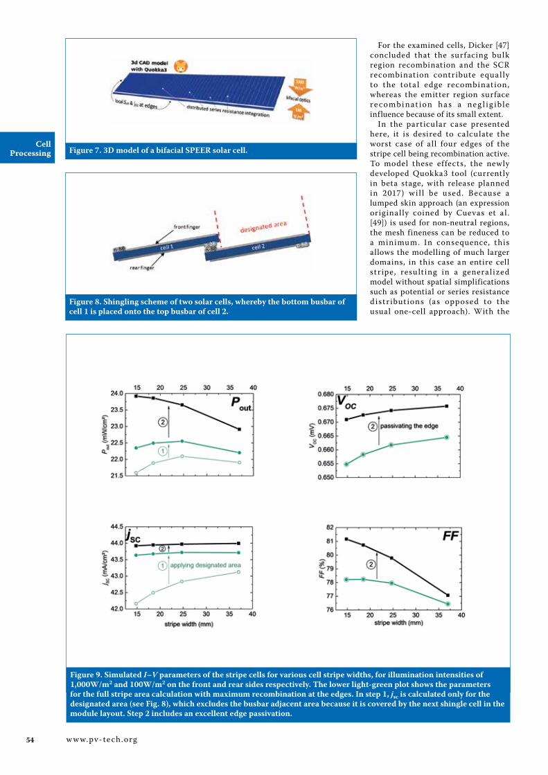
Figure 9. Simulated I–V parameters of the stripe cells for various cell stripe widths, for illumination intensities of 1,000W/m2 and 100W/m2 on the front and rear sides respectively. The lower light-green plot shows the parameters for the full stripe area calculation with maximum recombination at the edges. In step 1, jsc is calculated only for the designated area (see Fig. 8), which excludes the busbar adjacent area because it is covered by the next shingle cell in the module layout. Step 2 includes an excellent edge passivation.
Figure 7. 3D model of a bifacial SPEER solar cell.
Figure 8. Shingling scheme of two solar cells, whereby the bottom busbar of cell 1 is placed onto the top busbar of cell 2.

latest addition of a vertical resistance and full injection dependence on the skin parameterization [25], the skins can be described by lumped parameters without errors, compared with, for example, explicitly accounting for doping profiles. The cell stripe CAD model is depicted in Fig. 7.
“The goal of the cell optimization is to find the ideal cell stripe width and determine the
impact of edge recombination.”The input parameters are extracted from a bifacial PERC
solar cell that has been processed on the Fraunhofer ISE PV-TEC pilot line, yielding a front-side efficiency of 21% under 1,000W/m2 AM1.5g illumination and with a bifaciality of 75% (see Table 1); these parameters are then applied to the stripe cell, which is based on the same processes. The goal of the cell optimization is to find the ideal cell stripe width and determine the impact of edge recombination. Three scenarios are therefore simulated while varying the stripe width, beginning with a stripe cell with a highly recombinational edge (Seff and j02 as shown in Table 3).
As shown in Fig. 8, the busbar, as well as the adjacent area, is covered by an active area of the overlying cell; thus, only the marked designated area is relevant in the determination of the jsc. In step one (‘1’ in Fig. 9), this effect due to shingling in the module is included in the simulated I–V parameters. The second step (‘2’ in Fig. 9) introduces an excel lent edge passivation, assuming Seff = 10cm/s and j02,edge = 0nA/cm. All the results shown were calculated for a bifacial illumination with a front irradiance of 1,000W/m2 and a rear irradiance of 100W/m2 (which is presumed to be a candidate for a coming standard for bifacial I–V measurements).
Step 1 has a major ef fect on jsc, but the dependence on the stripe width vanishes as the continuous shading of the busbar is diminished. Moreover, jsc shifts by around 1mA/cm2, to 43.7mA/cm2, which ref lects one aspect of the advantages of shingling technology. Step 2, the edge passivation, manifests its ef fect mainly in FF and Voc. Reduced SCR recombination at the edges j02,edge leads to a jump in FF by 2–3%abs for small stripes; the reduced base edge recombination Seff increases Voc by 10–15mV for small stripes. Both effects are pronounced for small stripes as a result of their higher contour-to-area ratio.
Step 1 increases the overall power output Pout of the stripe cel l from 22 to 22.5mW/cm 2 at an ideal stripe width of 25mm, and reduces the sensitivity to variations in stripe width. Step 2 increases Pout to 23.6mW/cm2 at a stripe width of 25mm. It increases further with smaller stripe widths, but this is not a suitable approach for cell interconnection, as wil l be shown in the next section. Overall, with a gain of more than 1mW/cm2 it is well worth considering an additional process step for edge passivation. The implementation of such an edge passivation technique, which is in the best case also suitable for mass production, is currently a high-priority line of investigation in the ongoing work at Fraunhofer ISE.
Module integration and CTM loss analysisAs described above (see Fig. 8), the electrical interconnection of solar cells in shingled modules is achieved by overlapping and directly connecting the n and p sides of adjacent solar cells. To increase electrical performance, an electrically conductive adhesive (ECA) or solder paste may be used between the cell stripes [13]. The depth of the overlap is observed to be between 1 and 2mm. A trade-off in overlap between manufacturing requirements (cell lay-up
ILS-TT nx Next Generation Turntable Platform
InnoLas Solutions GmbHwww.innolas-solutions.com
Up to 6000 wafers per hour (w/h)
Multi process head con guration
Dual lane automation system
Laser Contact Opening for PERC
Laser Doped Selective Emitter
Front side LCO
Laser Direct Cleaving
HIGH THROUGHPUT LASER MACHINE
VISIT USINTERSOLAR
A2.455
56 w w w.pv- tech.org
Cell Processing
precision) and costs (shaded cel l parts do not generate power, but st i l l have to be purchased) needs to be examined, which is crucia l for the module’s power/price ratio. The same argument is valid for the size of the shingled cells: although smaller cel l stripes decrease some electrica l losses because of lower current generation, as shown in the previous model l ing, they increase manufacturing requirements, the proportion of overlapped area, and edge recombination losses.
S i n c e a l l c e l l s a r e d i r e c t l y connected, a string of signif icant length without gaps or compensating
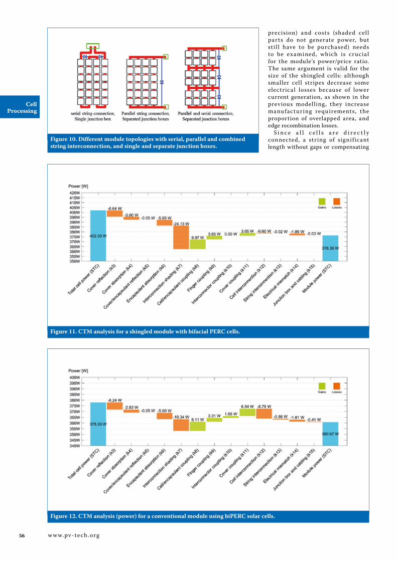
Figure 11. CTM analysis for a shingled module with bifacial PERC cells.
Figure 12. CTM analysis (power) for a conventional module using biPERC solar cells.
Figure 10. Different module topologies with serial, parallel and combined string interconnection, and single and separate junction boxes.

58 w w w.pv- tech.org
Cell Processing
elements is formed. At changing temperatures , thermomechanica l s t r e s s o c c u r s w i t h i n t h e c e l l i n t e r c o n n e c t i o n a n d t h e c e l l metallization. While the stress from external loads (e.g. snow) may be reduced by placing the solar cel ls in the neutral plane of double-glass modules, the thermomechanical stress resulting from different coefficients of thermal expansion cannot be avoided.
The direct overlapping of the cell stripes eliminates the cell gaps, and therefore increases the active module area proportion. Two options are possible to take advantage of the resulting gains: 1) reduce the module s i ze, keeping the modu le power constant and saving on module area and materials; or 2) keep the module area constant and increase power and efficiency. For typical set-ups, either approximately 9% more power than a conventional module can be generated, or the module area can be reduced.
A s a re s u l t o f t he i nc re a s e d number of (smaller) solar cel ls in shingled modules, the module voltage increases if a conventional module topology that connects strings of solar cells in series (Fig. 10) is used. To be compat ible w it h ex i s t i ng inverters, and so as not to exceed elec t r ica l l i m it at ion s , e lec t r ica l properties similar to conventional PV modu les a re des i rable . New module topologies featuring strings con nec ted i n pa ra l le l , or u s i ng combinations of parallel and serial cell and string interconnection, are therefore necessary and have been discussed in the literature [8,50,51].
Shingl ing requires new solut ions for string interconnection, junction boxes and bypass diode placement.
“Shingling requires new solutions for string
interconnection, junction boxes and bypass diode
placement.”Shingled modules are a concept
that is certainly capable of producing increased module ef f ic ienc y and modu le power. A deta i led CTM analysis using SmartCalc.CTM by Fraunhofer ISE [52] (also presented in another article in this issue of Photovoltaics International . p.97) reveals important gains and losses as well as several major differences with conventional modules.
First, a few remarks on the CTM-loss calculations have to be made. Shing l ing is the only cr ysta l l ine module concept in which the active cell area may be shaded by another act ive area. The overlapping cel l area usually has a higher efficiency, s i nc e t he over l app e d c e l l a re a features metallization patterns for interconnection.
Let us assume that two cel ls of t he sa me power a re completely overlapped, a nd t hat t he lower cel l is ful ly shaded and therefore produces no electrical power. Now, only one ‘power unit’ remains after this overlapping. Since the reference area has also changed, the efficiency
remains the same (CTMefficiency = 1). Because initially (before overlapping) t wo power producing cel l s were present, the CTM factor for power has changed and is now CTMpower = 0.5. With shingling, therefore, the CTM factors for power and efficiency do not correspond as they do with other module concepts.
Usually, the absolute power loss is higher for a shingled module than for a conventional one, but so is the sum of the initial cell powers, since more cells are needed to cover the module and the overlapping areas. Figs. 11 and 12 illustrate the higher absolute CTM losses for shingled modules. Never t heless , sh i ng led modu les a re capable of ach iev ing h ig her module powers and efficiencies than conventional modules [53].
Shingled modules do not include interconnection ribbons; thus, there are no electrical losses associated with ribbons, but contact and bulk resistance losses in the ECA occur. Opt ica l ga ins and losses remain practical ly unchanged from those of conventional modules, with the exception of backsheet ref lections (k11) and potential ref lective gains from interconnection ribbons (k10). Electrical mismatch losses are heavily dependent on the manufacturing equipment and the homogeneity of the cell stripes [54].
Sm a r t C a lc .C T M w a s u s e d t o analyse the CTM ratio of a shingled module using the modelled bifacial PERC cells described above; results of the analysis are shown in Fig. 11. The module features six strings of 67 shingled cells with dimension 25mm
Figure 13. CTM analysis (power) for a shingled module with 400Wp (257W/m2).

Photovoltaics International 59
Cell Processing
× 156mm. Each cell has a power of 1W (Pout = 23.2mW/cm2 at 1,000W/m 2 front-side and 100W/m 2 rear-side irradiance), which corresponds to the black line in Fig. 9 at 25mm, calculated using a full area instead of a designated area. Commercially available module materials – such as EVA, AR-coated glass and a polymer backsheet – are used. The overlap of the cells is set to 2mm; reducing this value would greatly reduce the total power loss from cell to module, but not the final module power. A module with SPEER cells would produce 376W (Pout = 21.9mW/cm2).
Full-size biPERC solar cells were used in a conventional module set-up (H-pattern, ribbon interconnection, 2 0 5m m pseudo -squa re , 6 W per bifacial cell), and a comparative CTM analysis of both module concepts was performed. Results of the ribbon-interconnected PERC cells are shown in Fig. 12. A conventional ribbon-interconnected module – featuring solar cel ls with the same biPERC technology as the previous SPEER cells – would only produce 361W.
Since an overlap of the shingled cells of 2mm was chosen, a larger number of cells is necessary for the shingled module (402Wp, Fig. 11). At this point, cost considerations become important and further module optimization is supported with SmartCalc.CTM.
To obtain a module power with the conventional module set-up that is similar to the power that can be achieved with the shingle concept, an increase in the initial cell performance is necessary for H-pattern biPERC c e l l s . B i f a c i a l H -p at t e r n c e l l s w it h 24 .2mW/cm 2 at 1,10 0W/m 2
irradiance (an increase of 1.0mW/cm2 compared with the SPEER cells for shingling) would be required to also achieve a module power of 376W. As the approach here features stripe cells based on the specific process technology for large-area cells, the power of the shingled module will automatica l ly surpass that of the conventional module technology by around this margin, even if the cell efficiencies improve.
The next step to reaching the target of 400W per module (at an area of a common 60-cell module) is to perform an estimation of the necessary cell power to achieve this goal. A detailed CTM analysis is shown in Fig. 13.
A parameter sweep of the electrical cell characteristics reveals that SPEER cells with 1.06Wp (Pout = 24.7mW/cm2) are required if a shingled module set-up as described above is used. Dividing that output power by 1.1 (irradiance factor), and neglecting
the bifaciality factor, the approximate front-side efficiency for such a cell would be η = 22.5%. This is a number wh ich, accord i ng to t he ITR PV roadmap [15], is to be expected for mass-cel ls produced by 2021, and has in fact already been achieved for full-size pseudo-square PERC record cells ([55], η = 22.61%). Furthermore, if the next-generation cell concepts discussed above, such as SHJ, are integrated in shingled modules, then powers exceeding 400W in standard-s i z e modu le s c a n def i n ite ly be expected.
SummaryP V mo dules w ith shing le d cel l technology have a history almost as old as the silicon solar cell itself. With bifacial PERC or PERC-like solar cells, industrially available concepts are at hand that now put shingling technology into an attractive position. A cost-effective cell concept can be boosted by the bifacial shingled module concept towards achieving the module power benchmark of 400W, for a conventional (‘60-cell’) module size with 1,000W/m2 front and 100W/m2 rear irradiance, by reducing CTM losses and benefitting from bifacial irradiance gains.
Some of the challenges faced on the path to realizing a bifacial shingled module have been highlighted:
1. Achievement of a monofacial cell efficiency of 22.5% (standard test conditions, 1,000W/m2 irradiance) in mass product ion, which i s supposed to be reached by PERC/PERT/PERL R&D in the next two years as a result of industry self-interest.
2. Provision of suitable cell separation techniques and/or reduction in edge recombination through appropriate passivation methods.
3. Development of reliable shingled cell interconnection and precise module assembly to guarantee durability and minimum mismatch in the module.
“It is the authors’ belief that the combination of shingling
and bifacial technology offers the greatest and most accessible levers for power output increases in solar
modules.”
The modularity of the shingling mo du le concept , toget her w it h the ava i labi l it y of the presented hybrid PERC (TopCon) or si l icon heterojunction concepts, furthermore implies the possibility of even higher module powers, which are basically a bonus when the module concept for biPERC has been developed. Overall, this is encouraging in the development of a product suitable for the industrial and consumer markets, because it i s the authors’ bel ief that the combination of shingling and bifacial technology of fers the greatest and most accessible levers for power output increases in solar modules. The recent appearance of the first shingled modules from large manufacturers seems to support the considerations discussed in this paper.
AcknowledgementsThe experiments in this work were conducted within the framework of the ‘PV-BAT400’ project (Contract No. 0324145), supported by the German Federal Ministry for Economic Affairs and Energy. The authors would like to thank all the people in the PMZ, PTQ and SEC teams at Fraunhofer ISE for their support and making this study possible.
References[1] Dickson, D.C., Jr. 1960, “Photo-
voltaic semiconductor apparatus or the like”, US Patent 2938938 (May 31).
[2] Chapin, D.M., Fu l ler, C .S. & Pea rson, G.L . 195 4 , “A new silicon p-n junction photocell for converting solar radiation into electrical power”, J. Appl. Phys., Vol. 25, No. 5, p. 676.
[3] Nielsen, R.J. & Lei f, R . 1963, “Satellite solar cell assembly”, US Patent 3116171 (Dec. 31).
[4] Myer, J.H. 1968, “Photovoltaic generator”, US Patent 3369939 (Feb. 20).
[5] Baron, W.R. 1969, “Solar cel ls w i t h f l e x i b l e o v e r l a p p i n g bifurcated connector”, US Patent 3459597 (Aug. 5).
[6] Gochermann, H. & Soll, J. 1996, “Shingle-type solar cell generator prodn. – a l lowing format ion of curved or domed product”, German Patent 3942205 (Feb. 1).
[7] Ya ng , B . e t a l . 2 015, “H ig h efficiency solar panel”, US Patent 14/563,867 (Apr. 2).
[8] Morad, R. et al. 2016, “Shingled solar cel l module”, US Patent 14/605,695 (Nov. 1).
[9] Mor ad, R . e t a l . , “Sh i ng led solar cel l module”, US Patent 14/572,206 (Jul. 26).
60 w w w.pv- tech.org
Cell Processing
[10] Morad, R. et al. 2016, “Shingled solar cel l module”, US Patent 14/594,439 (Jul. 19).
[11] Zhao, J. et al. 1997, “20000 PERL silicon cells for the ‘1996 World Solar Challenge’ solar car race”, Prog. Photovolt: Res. Appl., Vol. 5, No. 4, pp. 269–276.
[12] Glunz, S.W. et al. 2002, “High-efficiency silicon solar cells for low-illumination applications”, Proc . 29th IEEE PVSC , New Orleans, Louisiana, USA, pp. 450–453.
[13] Beaucarne, G. 2016, “Materials cha l lenge for sh i ng led cel l s i n t e r c o n n e c t i o n ” , E n e r g y Procedia, Vol. 98, pp. 115–124.
[14] SunPower Corporat ion 2017, “ S u n Powe r i nt r o duc e s ne w solar panel: The performance ser ies” [ht tps://us . su npower.com/blog/2015/11/12/sunpower-introduces-performance-series-solar-panel/].
[15] IT R PV 2 017, “ I nt er n at ion a l t e c h n o l o g y r o a d m a p f o r photovolt a ic ( IT R PV ): 2 016 results”, 8th edn (Mar.) [http://w w w . i t r p v . n e t / R e p o r t s /Downloads/].
[16] Kopecek, R. & Libal, J. 2017, “Quo vadis bifacial PV?”, Photovoltaics International, 35th edn.
[17] Blakers, A.W. et al. 1989, “22.8% efficient silicon solar cell”, Appl. Phys. Lett ., Vol. 55, No. 13, pp. 1363–1365.
[18] Zhao, J., Wang, A. & Green, M.A. 2001, “24.5% ef f iciency PERT silicon solar cells on SEH MCZ substrates and cell performance o n o t h e r S E H C Z a n d F Z substrates”, Sol . Energy Mater. Sol. Cells, Vol. 66, Nos. 1–4, pp. 27–36.
[19] Wang, A., Zhao, J. & Green, M.A. 1990, “24% efficient silicon solar cells”, Appl. Phys. Lett., Vol. 57, No. 6, pp. 602–604.
[20] N o r o u z i , M . H . e t a l . 2 0 1 7 , “ D e v e l o p m e n t a n d c h a r a c t e r i z a t i o n o f multifunctional PassDop layers for local p+-laser doping”, Energy Procedia [forthcoming].
[21] N o r o u z i , M . H . e t a l . 2 0 1 7, “ D e v e l o p m e n t a n d c h a r a c t e r i z a t i o n o f A l O x /SiNx:B layer systems for surface pa s s i v at ion a nd lo c a l l a s er dopi n g ”, I E E E J . Phot ovo l t . [forthcoming]
[22] S u w i t o , D . e t a l . 2 0 1 0 , “ I n d u s t r i a l l y f e a s i b l e r e a r p a s s i v at ion a nd c ont ac t i n g scheme for high-efficiency n-type solar cells yielding a Voc of 700 mV”, IEEE Trans. Electron Dev.,
Vol. 57, No. 8, pp. 2032–2036.[23] Wolf, S.D. et a l. 2012, “High-
efficiency silicon heterojunction solar cells: A review”, Green, Vol. 2, No. 1.
[24] F e l d m a n n , F. e t a l . 2 014 , “Passivated rear contacts for high-efficiency n-type Si solar cel ls providing high interface passivation quality and excellent transport characteristics”, Sol . Energy Mater. Sol. Cells, Vol. 120, pp. 270–274.
[25] Fell, A., Schubert, M.C. & Glunz, S.W. 2017, “The concept of skins for (silicon) solar cell modelling”, Sol . Energ y Mater. Sol . Cells [forthcoming].
[26] Biro, D. et al. 2006, “PV-TEC: P h o t o v o l t a i c t e c h n o l o g y evaluation center – Design and implementation of a production research unit”, Proc . 21st EU PVSEC, Dresden, Germany, pp. 621–624.
[27] Werner, S . et a l . 2017, “Key aspects for fabrication of p-type Cz-Si PERC solar cells exceeding 22% conversion efficiency”, Proc. 33rd EU PVSEC , Amsterdam, The Netherlands.
[28] S a i nt- C a s t , P. e t a l . 2 016 , “Analysis and outlook of near-industr ia l PERC solar cel l s”, Photovoltaics International, 34th edn, pp. 52–59.
[29] S a i nt- C a s t , P. e t a l . 2 017, “A n a l y s i s o f t h e l o s s e s o f industrial-type PERC solar cells”, physica status solidi (a), Vol. 214, No. 3, p. 1600708.
[30] Hezel, R. & Jaeger, K. 1989, “Low-temperature surface passivation of s i l icon for solar cel l s”, J . Electrochem. Soc., Vol. 136, No. 2, pp. 518–523.
[31] Aberle, A.G. & Hezel, R. 1997, “Progress in low-temperature surface passivat ion of si l icon solar cells using remote-plasma silicon nitride”, Prog. Photovolt: Res . Appl ., Vol. 5, No. 1, pp. 29–50.
[32] Hübner, A., Aberle, A.G. & Hezel, R. 1997, “20% efficient bifacial silicon solar cells”, Proc. 14th EU PVSEC, Barcelona, Spain, pp. 92–95.
[33] Krauß, K. et al. 2016, “biPERC s i l icon s ol a r ce l l s en abl i ng b i f a c i a l a p p l i c a t i o n s f o r i ndu s t r i a l s o l a r c e l l s w i t h passivated rear sides”, physica status solidi (a), Vol. 213, No. 1, pp. 68–71.
[34] W ö h r l e , N . e t a l . 2 0 1 7, “Understanding the rear-side layout of p-doped bifacial PERC solar cells with simulation driven
experiments”, Energy Procedia [forthcoming].
[35] D u l l we b e r, T. e t a l . 2 016 , “PERC+: Industrial PERC solar cells with rear Al grid enabling bifaciality and reduced Al paste consumption”, Prog. Photovolt: Res. Appl., Vol. 24, No. 12, pp. 1487–1498.
[36] F e l l m e t h , T. e t a l . 2 0 17, “Co-d i f f u sed bi-fac ia l PERT solar cel l s”, Energ y Procedia [forthcoming].
[37] Meier, S . e t a l . 2 017, “Fa s t co-diffusion process for bifacial n-type solar cells”, Solar RRL, Vol. 1, No. 1, p. 1600005.
[38] M e i e r , S . e t a l . 2 0 1 6 , “Co-diffusion for p-type PERT solar cel ls using APCVD BSG layers as boron doping source”, Proc. 32nd EU PVSEC, Munich, Germany.
[39] L o h mü l l e r, E . e t a l . 2 017, “Bi fac ia l p-t y pe PER L sola r c e l l s w i t h s c r e e n - p r i n t e d pu re A g me t a l l i z at ion a nd 89% bi fac ia l i t y ”, P roc . 33rd EU PVSEC , Amsterdam, The Netherlands.
[40] Adachi, D., Hernández, J.L . & Yamamoto, K . 2015, “Impact o f c a r r i e r r e c o m b i n a t i o n on f i l l fac tor for la rge a rea heterojunction crystalline silicon solar cell with 25.1% efficiency”, Appl. Phys. Lett., Vol. 107, No. 23, p. 233506.
[41] Strahm, B. 2017, “Heterojunction solar cel ls”, 7th nPV worksh., Freiburg, Germany.
[42] Benick, J. et a l . 2017, “High-e f f i c i e n c y m u l t i c r y s t a l l i n e n-type silicon solar cells”, Energy Procedia [forthcoming].
[43] Röth, J. et a l. 2015, “Thermal laser separation (TLS) dicing p r o c e s s s t u d y – A n e w technology for cutting si l icon solar cel ls for high-ef f iciency half-cell modules”, Proc. 31st EU PVSEC, Hamburg, Germany.
[44] Eiternick, S. et al. 2015, “High quality half-cell processing using thermal laser separation”, Energy Procedia, Vol. 77, pp. 340–345.
[45] L e w ke , D. 2 01 5 , “ T h e r m a l laser separation – TLS: Wafer-dicing der Zukunft” [www.iisb.f r au n hofe r.de/c ont ent /d a m /iisb2014/en/Documents/events/jahrestagung-2015/jt-2015-lewke.pdf].
[46] S a i nt- C a s t , P. e t a l . 2 010 , “High-efficiency c-Si solar cells passivated with ALD and PECVD aluminum oxide”, IEEE Electron Device Lett., Vol. 31, No. 7, pp. 695–697.

62 w w w.pv- tech.org
Cell Processing
[47] Dicker, J. 2003, “Analyse und Simulation von hocheffizienten Silizium-Solarzellenstrukturen f ü r i n d u s t r i e l l e F e r t i g u n g s t e c h n i k e n ” ( i n German), Dissertation, Faculty of Physics, University of Konstanz, Germany.
[48] Fell, A. et al. 2017, “A detailed analysis of edge related losses in half-cells”, Proc. 33rd EU PVSEC, Amsterdam, The Netherlands.
[49] Cuevas, A. et al. 2015, “Skin care for healthy silicon solar cells”, Proc . 42nd IEEE PVSC , New Orleans, Louisiana, USA, pp. 1–6.
[50] Su n Power C or p, “Su n Power P e r f o r m a n c e S e r i e s P 1 7 : Technical product datasheet”.
[51] Zhao, J. et al. 1997, “Improved ef f ic ienc y s i l icon sola r ce l l module”, IEEE Electron Device Lett., Vol. 18, No. 2, pp. 48–50.
[52] Mit tag , M. 2017, “Systematic PV-module optimization with the cell-to-module (CTM) analysis sof t w a re ‘Sma r t C a lc .C TM’”, Photovoltaics International, 36th edn.
[53] M it t ag , M . “Cel l-to-Modu le (CTM) Analysis for photovoltaic modules with sh ing led solar cel ls”, Proc . 44th IEEE PVSC, Washington DC, USA.
[54] Mittag, M. 2017, “Progress on unif ied cel l-to-module (CTM) determ i nat ion met hodolog y : Systematic calculation of module power”, Proc. 44th IEEE PVSC, Washington DC, USA.
[55] Clover, I . 2016, “Trina Solar sets new 22 .61% mono PERC efficiency record”, pv magazine (Dec.).
About the AuthorsNico Wöhrle studied physics at the University of Freiburg, Germany, and was awarded his diploma degree in 2012 f o r h i s w o r k a t
Fr au n hofer I SE on t he opt ic a l simulation of silicon solar cells. He received his Ph.D. from the University of Freiburg in 2016, with a topic involving the simulation of PERC solar cells. He is currently a researcher at Fraunhofer ISE, where he focuses on the simulation and modelling of solar cells, as well as on the conceptual development of p-type PERC solar cells.
E l m a r L o h m ü l l e r studied physics at the University of Tübingen, Germany, and at Nelson Mandela Metropolitan U n i v e r s i t y , P o r t
Elizabeth, South Africa. He received his diploma degree in 2010 for his work at Frau n hofer ISE on t he development of p-type MWT-PERC solar cells, followed by his Ph.D. from the University of Freiburg in 2015 for his contributions to the development of n-type MWT solar cel ls. He is currently a researcher at Fraunhofer ISE, with a focus on the development of p-type PERC solar cells.
Ma x M it t ag s t ud ied industrial engineering and management at the Freiberg University of Mining and Technology. In 2010 he completed
his diploma thesis at Fraunhofer ISE a n d j o i n e d t h e P V m o d u l e d e p a r t m e nt . H i s c u r re nt work includes CTM efficiency analysis and the development of new PV module concepts.
Anamaria Moldovan studied chemistry at the Universit y of Zurich, Sw it z er l a nd , a nd i n F r e i b u r g , G e r m a n y, receiving her diploma
deg ree i n 2 011 for her work at Fraunhofer ISE on wet chemica l cleaning. She was awarded her Ph.D. by the University of Freiburg in 2016 for her investigations of cleaning and cond it ion ing for h ig h-ef f ic ienc y silicon solar cells. She is currently a researcher at Fraunhofer ISE, focusing on the development of wet chemical and plasma processes for solar cells with passivated contacts.
P u z a n t B a l i o z i a n obt a i ne d a B . S c . i n physics in 2014 from the American University of B e i r u t . I n 2 016 h e received his M.Sc. in
renewable energy engineering and management from the University of Freiburg for his thesis work completed at Fraunhofer IPM in the f ield of magnetocaloric energy conversion. He is current ly a Ph.D. candidate at Fraunhofer ISE, where his main area of research is the development of p-type SPEER solar cells.
T o b i a s F e l l m e t h studied physics at the University of Konstanz, Germany, and received his diploma degree in 20 09 for h is work at
Fraunhofer ISE on the development a nd c h a r ac t e r i z at i o n o f M W T concentrator solar cel l s . He was awarded his Ph.D. by the University of Tübingen in 2014 for his studies of
silicon-based, low-concentrator solar cells. He is currently a scientist at Fraunhofer ISE, where he focuses on the development of bifacial p-type PERC solar cells.
Karin Krauss studied physics at the Albert Ludwig Universit y of Freiburg and received her diploma degree in 2012. Since 2013 she has
been working towards her Ph.D. at Fraunhofer ISE. She joined the PV production technology and quality assurance division at Fraunhofer ISE in 2011, where her research interests involve multicrystalline silicon solar cells and light-induced degradation.
Achim Kraft studied electrical engineering at the University of Applied Sc ience i n Ha nover, Germany, and renewable energies at the University
of Applied Science in Berlin. He received his master’s in renewable energies, before joining Fraunhofer ISE in 2012 as a Ph.D. student. He was awarded his Ph.D. in the field of plated-copper front-side metallizations for silicon solar cells by the Albert Ludwig University of Freiburg in 2015. Since then he has focused on solar cell interconnection technologies and processes as head of the interconnection technologies team in the module research group at Fraunhofer ISE.
Ralf Preu is director of t h e P V p r o d u c t i o n technology division at F r a u n h o f e r I S E i n Freiburg, Germany, and also teaches PV at the
University of Freiburg. He studied physics at the Universities of Freiburg and Toronto, and economics at the University of Hagen, Germany. He holds a Ph.D. in electrical engineering, and joined Fraunhofer ISE in 1993. His work in different fields in PV includes system monitoring, and silicon solar c e l l a n d m o d u l e t e c h n o l o g y, characterization and simulation, but his main focus is R&D in advanced silicon solar cell technology and its transfer to industrial production.
EnquiriesNico WöhrleFraunhofer Institute for Solar Energy Systems ISEHeidenhofstraße 279110 Freiburg, Germany
Tel: +49 (0)761 4588 5964Email: [email protected]