SOI SOI detectordetector SOI detector -...
42
W.Kucewicz A Vertex Detector for the ILC; Ringberg Castle; May 28 - 31, 2006 1 SOI detector (SUCIMA project) SOI SOI detector detector (S (S UCIMA UCIMA project project ) ) Wojciech Kucewicz Wojciech Kucewicz AGH-Univ. of Science and Technology, On behalf of the SUCIMA Collaboration
Transcript of SOI SOI detectordetector SOI detector -...

W.Kucewicz A Vertex Detector for the ILC; Ringberg Castle; May 28 - 31, 2006 1
SOI detector(SUCIMA project)
SOI SOI detectordetector(S(SUCIMA UCIMA projectproject))
Wojciech KucewiczWojciech KucewiczAGH-Univ. of Science and Technology,
On behalf of the SUCIMA Collaboration

W.Kucewicz A Vertex Detector for the ILC; Ringberg Castle; May 28 - 31, 2006 2
OutlineOutlineOutline
Principle of the SOI sensor and Principle of the SOI sensor and technology sequencetechnology sequence
Preliminary test of the small area SOI Preliminary test of the small area SOI sensors on the high resistive substratessensors on the high resistive substrates
The full size SOI sensor The full size SOI sensor –– layout, layout, readout scheme and first measurementsreadout scheme and first measurements

W.Kucewicz A Vertex Detector for the ILC; Ringberg Castle; May 28 - 31, 2006 3
The main goal of the project was the
DEVELOPMENT OF AN ADVANCED IMAGING DEVELOPMENT OF AN ADVANCED IMAGING TECHNIQUETECHNIQUE OF EXTENDED RADIOACTIVE SOURCES USED IN OF EXTENDED RADIOACTIVE SOURCES USED IN
MEDICAL APPLICATIONSMEDICAL APPLICATIONS
Where “imaging” has be intended as the record of a dose map
Development & boundary conditions were defined by the specific end-user requirements:
BrachytherapyBrachytherapyHadrontherapyHadrontherapy
SUCIMASUCIMAThe collaboration The collaboration waswas made out of 9 Dept.made out of 9 Dept.’’s or Research Centers s or Research Centers and 2 companies from 5 EU countries.and 2 companies from 5 EU countries.
W.Kucewicz A Vertex Detector for the ILC; Ringberg Castle; May 28 - 31, 2006 4
Axial view
High activity seedMedium activity seedLow activity seed
Target
Online dose measurement inBrachytherapy
Online dose measurement inBrachytherapy

W.Kucewicz A Vertex Detector for the ILC; Ringberg Castle; May 28 - 31, 2006 5
Hadrontherapy:real-time beam monitoring
Hadrontherapy:Hadrontherapy:realreal--time time beam beam monitoringmonitoring
Basic principle:Basic principle: collection and imaging of secondary electrons emitted by thin Aluminum foils as the beam is delivered
vacuum chamber
HV
secondary emission foil
electron detector
PROFILE/CURRENT MEASUREMENT
beam
SLIMSLIM ≡ Secondary Emission for Low Interception Monitoring
W.Kucewicz A Vertex Detector for the ILC; Ringberg Castle; May 28 - 31, 2006 6
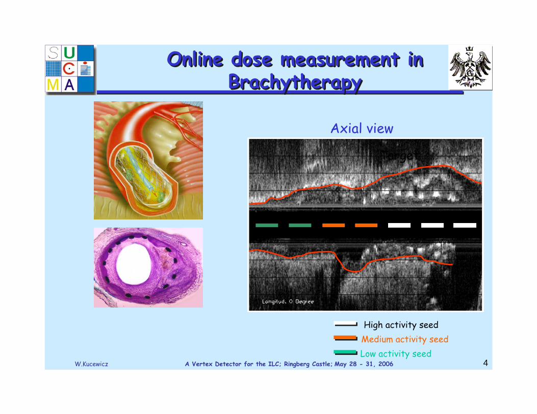
SOI Detector IdeaSOISOI DDetectoretector IdeaIdea
Readout electronicsReadout electronics
Silicon Silicon sensorsensor
On On the the same same waferwaferIs it possibleIs it possible??
W.Kucewicz A Vertex Detector for the ILC; Ringberg Castle; May 28 - 31, 2006 7
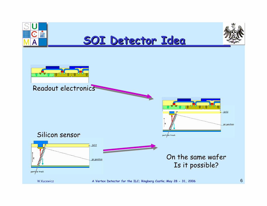
SOI Detector IdeaSOISOI DDetectoretector IdeaIdeaThe The wafer bondingwafer bonding techniques was chosen for SOI techniques was chosen for SOI
technologytechnology
Low resistivity
High resistivity
SIO2
SIO2
High resistivity
SIO2SIO2Thin low Thin low resistivityresistivity layer layer –– readout readout
electronics circuitelectronics circuit
High High resistivityresistivity support support –– sensitive areasensitive area
Termochemical bonding
11--1,5 1,5 μμmm
High resistivity
SIO2
Low resistivity
SIO2

W.Kucewicz A Vertex Detector for the ILC; Ringberg Castle; May 28 - 31, 2006 8
SOI Detector IdeaSOISOI DDetectoretector IdeaIdea

W.Kucewicz A Vertex Detector for the ILC; Ringberg Castle; May 28 - 31, 2006 9
SOI Detector SOISOI Detector Detector Advantages:Advantages:
•• The SOI sensor may merge the The SOI sensor may merge the advantages of the monolithic and advantages of the monolithic and hybrid detectorshybrid detectors
As a monolithic device eliminates bumpAs a monolithic device eliminates bump--bonding process and allows reductionbonding process and allows reductionof total sensor thickness of total sensor thickness reduction ofreduction of multiple scatteringmultiple scattering
Allows using high resistive detector substrates and operation inAllows using high resistive detector substrates and operation in fully fully depleted region depleted region good detection efficiency, enables detection of particles good detection efficiency, enables detection of particles with limited range in the silicon without with limited range in the silicon without backthinningbackthinning processprocess))
Gives possibility to use both type of transistors in readout chaGives possibility to use both type of transistors in readout channels nnels increased flexibility of the design, design optimisation for difincreased flexibility of the design, design optimisation for different ferent applicationapplication

W.Kucewicz A Vertex Detector for the ILC; Ringberg Castle; May 28 - 31, 2006 10
SOI Detector SOISOI Detector Detector
Disadvantages:Disadvantages:•• Needs a new technology developmentNeeds a new technology development
•• Relatively small size sensor limited by technology limitsRelatively small size sensor limited by technology limits

W.Kucewicz A Vertex Detector for the ILC; Ringberg Castle; May 28 - 31, 2006 11
SOI Detector TechnologySOISOI DDetectoretector TechnologyTechnology
Etching of the cave forEtching of the cave for pnpn junctionjunction
NN typetype,, Low resistivityLow resistivitySiOSiO22
NN typetype,, High resistivityHigh resistivity
W.Kucewicz A Vertex Detector for the ILC; Ringberg Castle; May 28 - 31, 2006 12
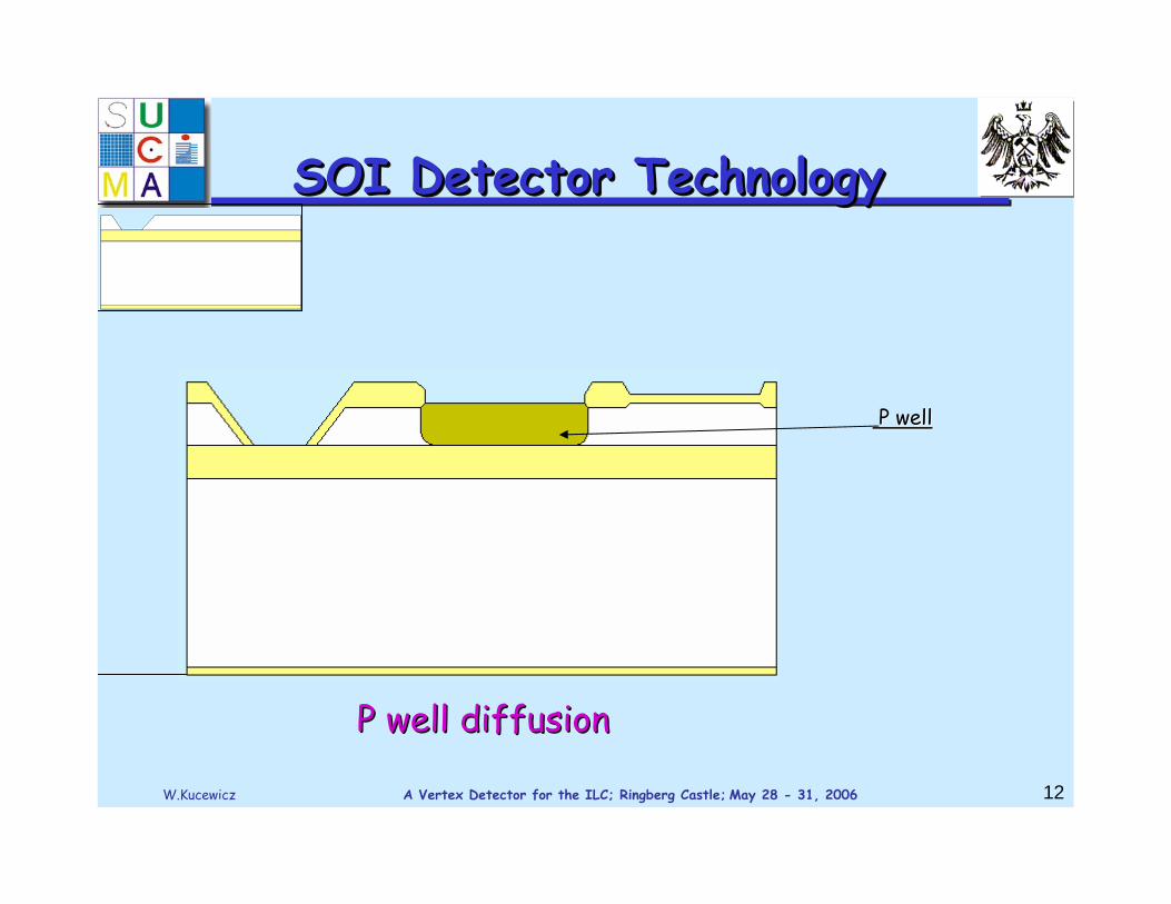
SOI Detector TechnologySOISOI DDetectoretector TechnologyTechnology
P P well diffusionwell diffusion
PP wellwell

W.Kucewicz A Vertex Detector for the ILC; Ringberg Castle; May 28 - 31, 2006 13
SOI Detector TechnologySOISOI DDetectoretector TechnologyTechnology
P & N diffusion of channel stoppers to P well & substrateP & N diffusion of channel stoppers to P well & substrate
P+P+
N+N+
W.Kucewicz A Vertex Detector for the ILC; Ringberg Castle; May 28 - 31, 2006 14
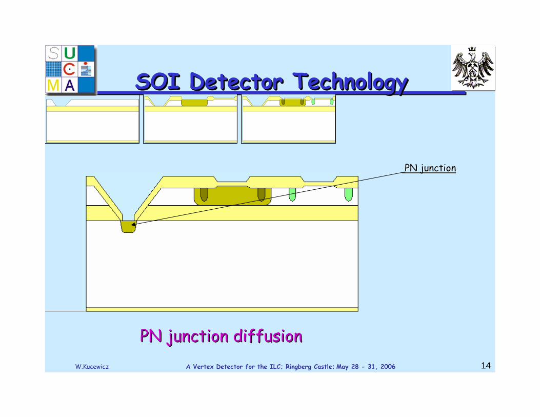
SOI Detector TechnologySOISOI DDetectoretector TechnologyTechnology
PN PN junction diffusion junction diffusion
PN PN junctionjunction

W.Kucewicz A Vertex Detector for the ILC; Ringberg Castle; May 28 - 31, 2006 15
SOI Detector TechnologySOISOI DDetectoretector TechnologyTechnology
PolysiliconPolysilicon deposition deposition
PolysiliconPolysilicon

W.Kucewicz A Vertex Detector for the ILC; Ringberg Castle; May 28 - 31, 2006 16
SOI Detector TechnologySOISOI DDetectoretector TechnologyTechnology
Source Source & & drain implantationdrain implantation
NMOSNMOS
PMOSPMOS

W.Kucewicz A Vertex Detector for the ILC; Ringberg Castle; May 28 - 31, 2006 17
SOI Detector TechnologySOISOI DDetectoretector TechnologyTechnology
First First metal metal layerlayer
Metal 1Metal 1
W.Kucewicz A Vertex Detector for the ILC; Ringberg Castle; May 28 - 31, 2006 18
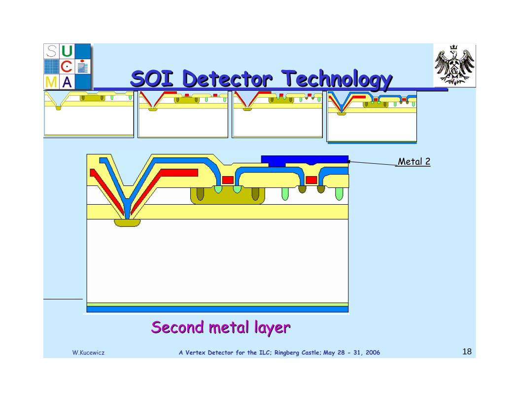
SOI Detector TechnologySOISOI DDetectoretector TechnologyTechnology
Second metal layer Second metal layer
Metal 2Metal 2

W.Kucewicz A Vertex Detector for the ILC; Ringberg Castle; May 28 - 31, 2006 19
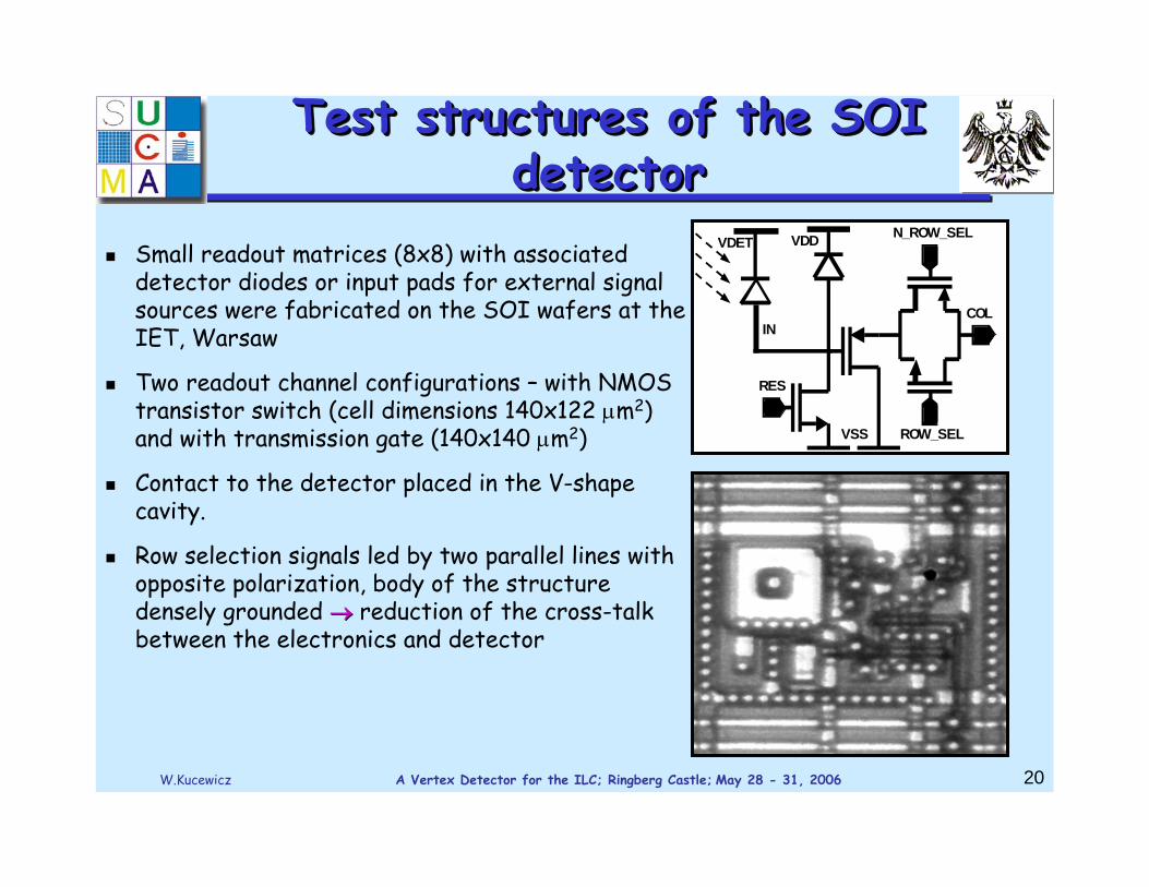
Test structures of the SOI detector
Test structures of the SOI Test structures of the SOI detectordetector
W.Kucewicz A Vertex Detector for the ILC; Ringberg Castle; May 28 - 31, 2006 20
Test structures of the SOI detector
Test structures of the SOI Test structures of the SOI detectordetector
Small readout matrices (8x8) with associated detector diodes or input pads for external signal sources were fabricated on the SOI wafers at the IET, Warsaw
Two readout channel configurations – with NMOS transistor switch (cell dimensions 140x122 μm2) and with transmission gate (140x140 μm2)
Contact to the detector placed in the V-shape cavity.
Row selection signals led by two parallel lines with opposite polarization, body of the structure densely grounded →→ reduction of the cross-talk between the electronics and detector
VDET
VSS
VDD
IN
RES
N_ROW_SEL
ROW_SEL
COL
W.Kucewicz A Vertex Detector for the ILC; Ringberg Castle; May 28 - 31, 2006 21
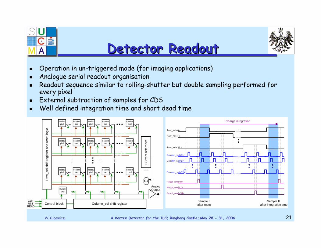
Detector ReadoutDDetectoretector RReadouteadoutOperation in un-triggered mode (for imaging applications)Analogue serial readout organisationReadout sequence similar to rolling-shutter but double sampling performed for every pixelExternal subtraction of samples for CDSWell defined integration time and short dead time
Readout pixel
Readout pixel
Readout pixel
Readout pixel
Readout pixel
Readout pixel
Readout pixel
Readout pixel
Readout pixel
Readout pixel
Readout pixel
Readout pixel
Readout pixel
Readout pixel
Readout pixel
Row
_sel
shi
ft re
gist
er a
nd re
set l
ogic
Analog Output
Column_sel shift register
Dummy pixel
Control block CLK RST
READ
Cur
rent
refe
renc
e
Row_sel<0>
Column_sel<0>
Column_sel<1>
Column_sel<31>
Reset_rowl<0>
Row_sel<1>
Row_sel<31>
Reset_rowl<1>
Reset_rowl<31>
Sample I-after reset
Sample II-after integration time
Charge integration

W.Kucewicz A Vertex Detector for the ILC; Ringberg Castle; May 28 - 31, 2006 22
SUCIMA Imager DAQ for the SOI DetectorSUCIMA Imager DAQ SUCIMA Imager DAQ for the SOI Detectorfor the SOI Detector
The DAQ is equipped with 4 independent 4 independent analogue inputanalogue input channels channels with 12 bit ADCs, 1MB fast static RAM, the FPGA Virtex II XC2V1000 chip for advanced algorithms and the high speed USB 2.0 portUSB 2.0 port for a fast data transfer to and from a PC computer.
GUI – developed in LabVIEW environment, allows setting: the matrix size to be readout, readout frequency;It provides: the CDS or last frame readout mode, masking noisy pixels, subtracting pedestals, suppressing signals bellow threshold and writing data to the file.
VIRTEX IIXC2V1000
4FG456CES(324 I/O)
VIRTEX IIXC2V1000
4FG456CES(324 I/O)
40 MHz
BANK_7SE
NSO
R
SUCIMA_IMAGER
BANK_2 BANK_3
BA
NK
_5B
AN
K_4
BANK_6
BA
NK
_0B
AN
K_1
S RA
M
2x25
6Kx 1
6B
S RA
M
2x25
6Kx1
6B
USB
& 2
8 G
P IO
pi n
s
D32A18
D24
D16
.
JTA
G
A18
A18CLK
CTRL
328 USER’s I/O PADS
SEN
SOR
’S R
EPE
AT
ER
SRA
M
2x25
6Kx1
6B
S RA
M
2x25
6Kx1
6B XV18V04
EEPROM
DedicatedDedicated DAQ system calledDAQ system called„„SUCIMA imagerSUCIMA imager”” was was developeddeveloped for for
the SUCIMA projectthe SUCIMA project by INF by INF in Cracowin Cracow..
14 cm14 cm
9.5
cm9.
5 cm
W.Kucewicz A Vertex Detector for the ILC; Ringberg Castle; May 28 - 31, 2006 23
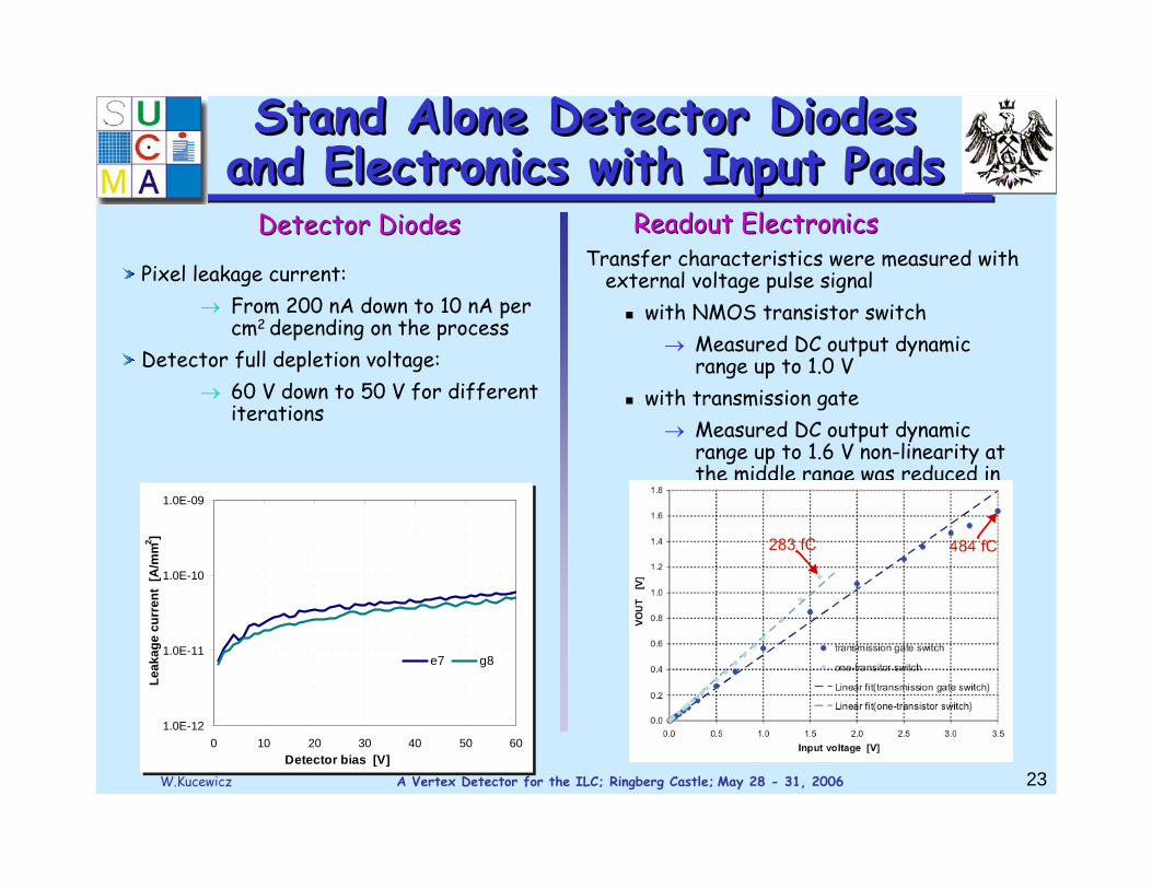
Stand Alone Detector Diodes and Electronics with Input PadsStand Alone DetectorStand Alone Detector Diodes Diodes
and Electronics withand Electronics with Input PadsInput Pads
Transfer characteristics were measured with external voltage pulse signal
with NMOS transistor switch → Measured DC output dynamic
range up to 1.0 Vwith transmission gate→ Measured DC output dynamic
range up to 1.6 V non-linearity at the middle range was reduced in the latest designs
Readout ElectronicsReadout Electronics
1.0E-12
1.0E-11
1.0E-10
1.0E-09
0 10 20 30 40 50 60Detector bias [V]
Leak
age
curr
ent
[A/m
m2 ]
e7 g8
1.0E-12
1.0E-11
1.0E-10
1.0E-09
0 10 20 30 40 50 60Detector bias [V]
Leak
age
curr
ent
[A/m
m2 ]
e7 g8
Pixel leakage current:→ From 200 nA down to 10 nA per
cm2 depending on the process Detector full depletion voltage:
→ 60 V down to 50 V for different iterations
Detector DiodesDetector Diodes

W.Kucewicz A Vertex Detector for the ILC; Ringberg Castle; May 28 - 31, 2006 24
Tests with the Laser LightTests Tests wwithith the Laser Lightthe Laser Light
Laser light not focused, shining from the backplane (biased by a metal mash)Wavelength = 850 nm4 μs wide light pulses – simulate particles passing through detector active volumeIntegration time = 1 msDetector polarization=60V10 000 events recorded and averagedInput signal scaled assuming the sensor gain of 11mV/MIP
GGood detector sensitivity for the ionising radiation and linear ood detector sensitivity for the ionising radiation and linear response as a function of the generated charge was observedresponse as a function of the generated charge was observed..
Linearity of Sensor ResponseLinearity of Sensor Response
W.Kucewicz A Vertex Detector for the ILC; Ringberg Castle; May 28 - 31, 2006 25
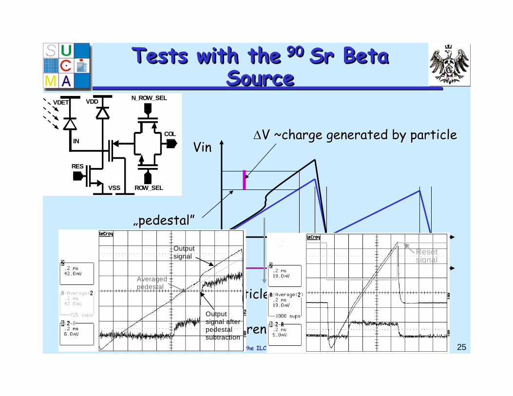
VDET
VSS
VDD
IN
RES
N_ROW_SEL
ROW_SEL
COL
tt
VinVin
RESRES
VinVin = (= (~ ~ leakage current leakage current + charge + charge collectioncollection))
„„pedestalpedestal””
ΔΔV ~charge V ~charge generatedgenerated by by particleparticle
Passing particlePassing particle
Output signal
Averaged pedestal
Output signal after pedestal subtraction
Resetsignal
Output signal
Averaged pedestal
Output signal after pedestal subtraction
Resetsignal
Tests with the 90 Sr Beta Source
Tests with theTests with the 90 90 SrSr Beta Beta SourceSource

26
Tests with the 90 Sr Beta SourceTests with theTests with the 90 90 SrSr Beta SourceBeta SourceSensor sensitivity tested with 90Sr beta sourceMeasurements conditions: complete depletion (Vdet= 60 V), integration time: Tint = 420 μs, source placed at the top of the sensor.Detector output signal amplified (4.5 ADC/mV) before digitalisationsOn-line CDS processing, off-line pedestal subtraction, common mode suppression and cluster search
Gaussian distribution of the noise
Landau distribution of the measured signals
The most probably value of signal per MIP: 5151 ADCADCNoise for the seed pixels:1.1.,8,8 ADCADC (670 e(670 e--))
19200 e19200 e
W.Kucewicz A Vertex Detector for the ILC; Ringberg Castle; May 28 - 31, 2006 27
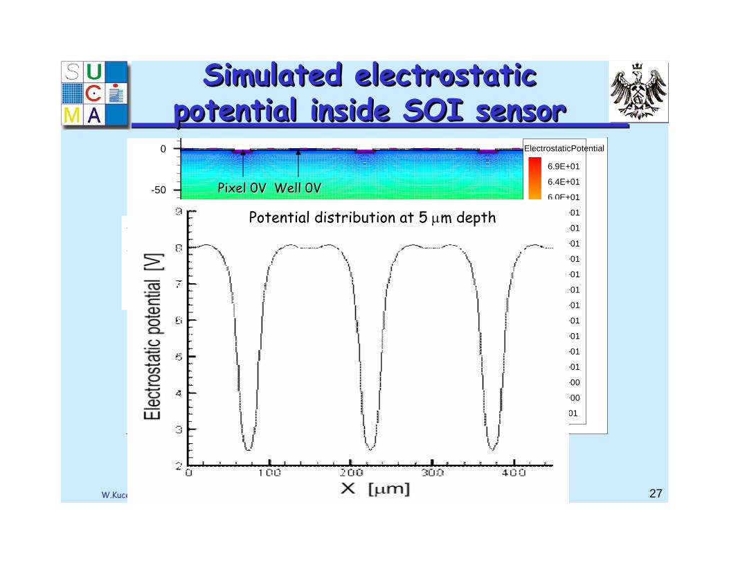
Simulated electrostatic potential inside SOI sensor
Simulated electrostatic Simulated electrostatic potential inside SOI sensorpotential inside SOI sensor
X
Y
0 100 200 300 400-300
-250
-200
-150
-100
-50
0 ElectrostaticPotential
6.9E+01
6.4E+01
6.0E+01
5.6E+01
5.1E+01
4.7E+01
4.3E+01
3.8E+01
3.4E+01
3.0E+01
2.5E+01
2.1E+01
1.7E+01
1.2E+01
8.2E+00
3.8E+00
-5.0E-01
PixelPixel 0V0V Well Well 0V0V
Sens
orSe
nsor
dept
hde
pth Potential distribution at Potential distribution at 5 5 μμmm depthdepth

W.Kucewicz A Vertex Detector for the ILC; Ringberg Castle; May 28 - 31, 2006 28
Tests with the Alpha ParticlesTests with theTests with the Alpha ParticlesAlpha Particles
Alpha source placed at the distance of 1 cm from the detector backplaneInitial energy of particles = 5.5 MeVDetector fully depleted (VD=70V), integration time 720 μsOn-line CDS processing, off-line pedestal subtraction, common mode suppression and cluster search

W.Kucewicz A Vertex Detector for the ILC; Ringberg Castle; May 28 - 31, 2006 29
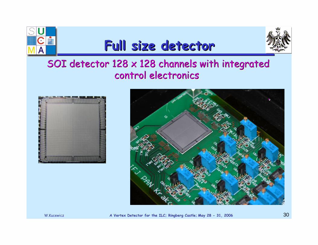
Design of a full size detector layoutDesign of a full size detector layoutDesign of a full size detector layoutDimensions: 24x24 mm2
128 x 128 = 16 384 channels4 sub-segments with independent parallel analogue outputsCell dimensions: 150x150μm2
Possibility to extend to ladders with dimensions up to 72x24 mm2 and small dead areas
Row
_sel
Col_sel
ADC
10.24mm 12mm
<0-63>
<0-6
3>
10.2
4mm
12m
m
ADC
ADCADC
ADC ADC
ADCADC
ADC
24mm
24m
m
72mm
24m
m
a) b)
c)
PixelPixelcavitycavity
W.Kucewicz A Vertex Detector for the ILC; Ringberg Castle; May 28 - 31, 2006 30
Full size detectorFFullull size detectorsize detector
, , ,
SOI detector 128 x 128 channels with integrated control electronics
SOI detector 128 x 128SOI detector 128 x 128 channelschannels with with integrated integrated controlcontrol electronicselectronics

W.Kucewicz A Vertex Detector for the ILC; Ringberg Castle; May 28 - 31, 2006 31
Full size detector - Tests with thelaser light
FFullull size detectorsize detector -- Tests with theTests with thelaser laser lightlight
Visualization of the readout results obtained with the best fullVisualization of the readout results obtained with the best full size size SOI detector and laser pointer light shined on two different SOI detector and laser pointer light shined on two different
quarters of the readout matrixquarters of the readout matrix

W.Kucewicz A Vertex Detector for the ILC; Ringberg Castle; May 28 - 31, 2006 32
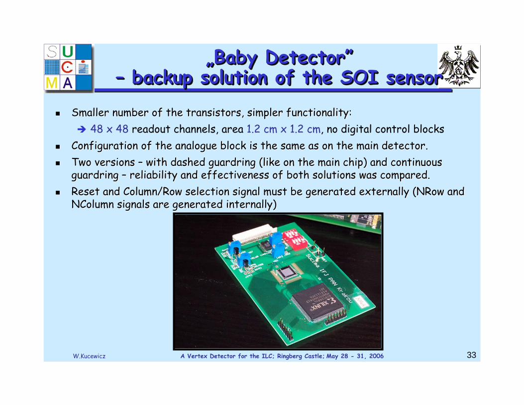
„Baby Detector”– backup solution of the SOI sensor
„„Baby DetectorBaby Detector””–– backup solution of the SOI sensorbackup solution of the SOI sensor
Smaller number of the transistors, simpler functionality: Smaller number of the transistors, simpler functionality: 48 x 48 readout channels, area 1.2 cm x 1.2 cm, no digital control blocks
Configuration of the analogue blockConfiguration of the analogue block isis the same as on the main detectorthe same as on the main detector..Two versions Two versions –– with dashed with dashed guardringguardring (like on the main chip) and continuous (like on the main chip) and continuous guardringguardring –– reliability and effectiveness of both solutions reliability and effectiveness of both solutions waswas compared.compared.Reset and Column/Row selection signal must be generated externalReset and Column/Row selection signal must be generated externallyly ((NRowNRow and and NCNColumnolumn signals are generated internallysignals are generated internally))
Dashed Dashed guardringguardring Continuous Continuous guardringguardring
W.Kucewicz A Vertex Detector for the ILC; Ringberg Castle; May 28 - 31, 2006 33
„Baby Detector”– backup solution of the SOI sensor
„„Baby DetectorBaby Detector””–– backup solution of the SOI sensorbackup solution of the SOI sensor
Smaller number of the transistors, simpler functionality: Smaller number of the transistors, simpler functionality: 48 x 48 readout channels, area 1.2 cm x 1.2 cm, no digital control blocks
Configuration of the analogue blockConfiguration of the analogue block isis the same as on the main detectorthe same as on the main detector..Two versions Two versions –– with dashed with dashed guardringguardring (like on the main chip) and continuous (like on the main chip) and continuous guardringguardring –– reliability and effectiveness of both solutions reliability and effectiveness of both solutions waswas compared.compared.Reset and Column/Row selection signal must be generated externalReset and Column/Row selection signal must be generated externallyly ((NRowNRow and and NCNColumnolumn signals are generated internallysignals are generated internally))
W.Kucewicz A Vertex Detector for the ILC; Ringberg Castle; May 28 - 31, 2006 34
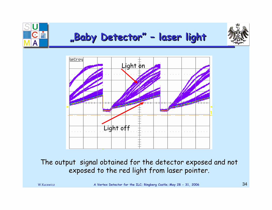
Light off
Light on
Light off
Light on
TThe output signal obtained for the detector exposed and not he output signal obtained for the detector exposed and not exposed to the red light from laser pointer.exposed to the red light from laser pointer.
„Baby Detector” – laser light„„Baby DetectorBaby Detector”” –– laser laser lightlight
W.Kucewicz A Vertex Detector for the ILC; Ringberg Castle; May 28 - 31, 2006 35
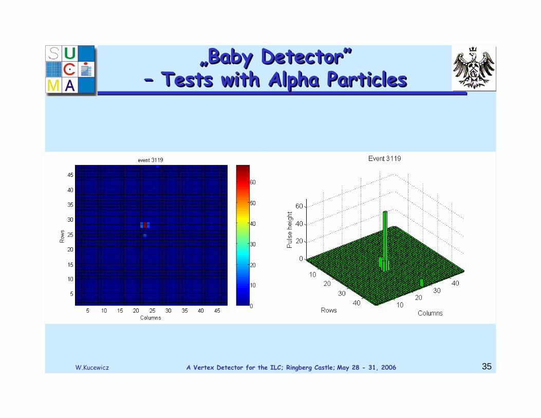
„Baby Detector”– Tests with Alpha Particles
„„Baby DetectorBaby Detector””–– Tests with Tests with Alpha ParticlesAlpha Particles

W.Kucewicz A Vertex Detector for the ILC; Ringberg Castle; May 28 - 31, 2006 36
„Baby Detector”– Tests with Beta Particles
„„Baby DetectorBaby Detector””–– Tests with Tests with BetaBeta ParticlesParticles

W.Kucewicz A Vertex Detector for the ILC; Ringberg Castle; May 28 - 31, 2006 37
ConclusionsConclusionsConclusionsFirst small area SOI pixel sensors have been fabricated.First small area SOI pixel sensors have been fabricated.The tests The tests results proveresults prove::
sensitivity of the test matrices for the MIP signals (measurements with 90Sr), wide dynamic range (measurements with laser spot and alpha particles), detector suitability for the detection of particles with limited range in silicon(measurements with alpha particles), effectiveness of the charge integration mechanism implemented in the readout circuit.
A larger and fully functional SOI sensor (128x128 readout channeA larger and fully functional SOI sensor (128x128 readout channels, active area of ls, active area of 2 cm x 2 cm, optimised for medical imaging applications) have be2 cm x 2 cm, optimised for medical imaging applications) have been designed and en designed and produced but only one produced but only one „„Baby detectorBaby detector”” was working.was working.
Next baNext batch tch of sensor with modified layout (smaller noof sensor with modified layout (smaller no polysiliconpolysilicon in the cave) will in the cave) will bebe applied soon.applied soon.
W.Kucewicz A Vertex Detector for the ILC; Ringberg Castle; May 28 - 31, 2006 38
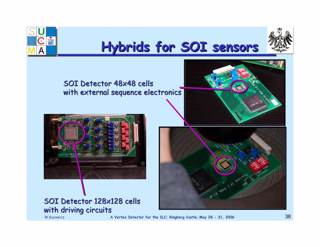
Hybrids for SOI sensorsHybrids Hybrids for SOI for SOI sensorssensors
SOI SOI DetectorDetector 128x128 128x128 cells cells with driving circuits with driving circuits
SOI SOI DetectorDetector 48x48 48x48 cellscellswith external sequence electronicswith external sequence electronics

W.Kucewicz A Vertex Detector for the ILC; Ringberg Castle; May 28 - 31, 2006 39
Measurements setupMeasurements setupMeasurements setup
SOI test SOI test structurestructure
SOI SOI final final sensorsensor
W.Kucewicz A Vertex Detector for the ILC; Ringberg Castle; May 28 - 31, 2006 40
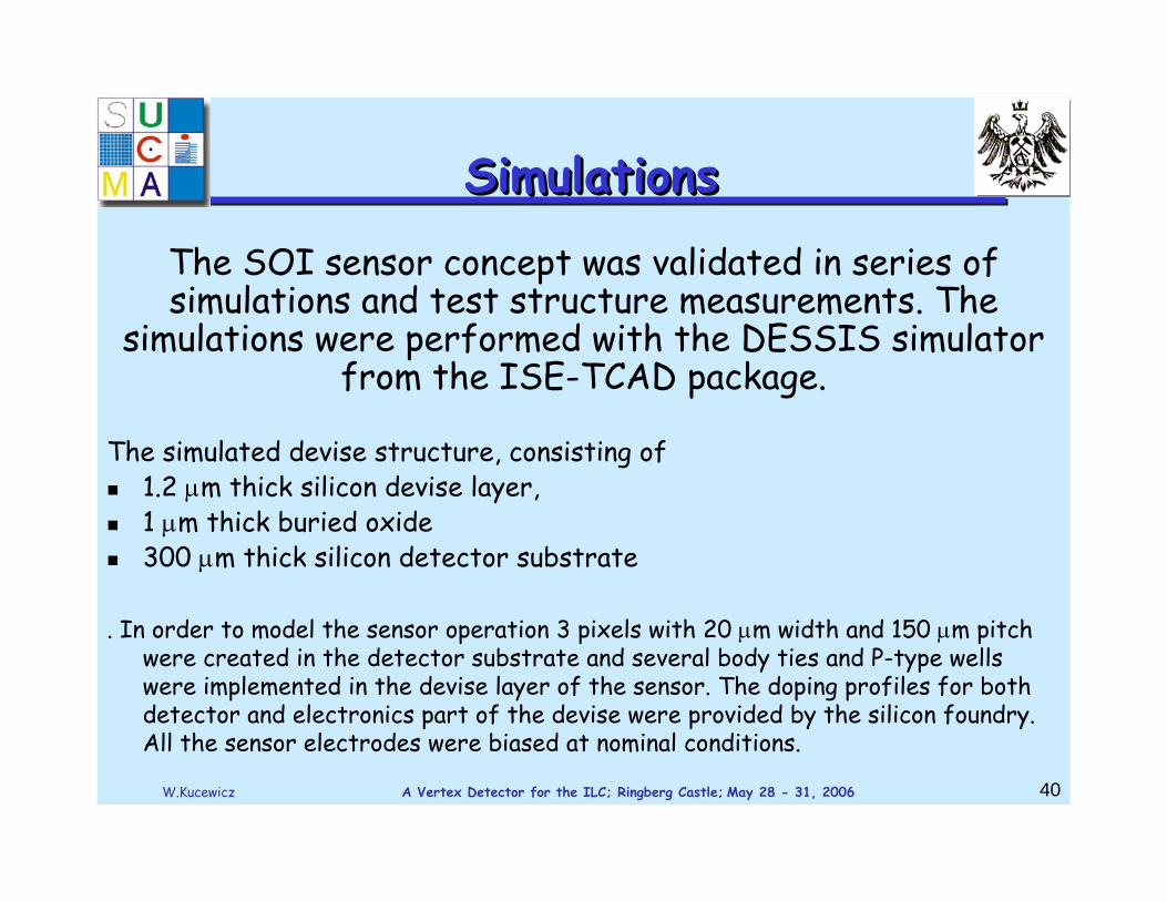
SimulationsSimulationsSimulations
The simulated devise structure, consisting of 1.2 μm thick silicon devise layer, 1 μm thick buried oxide 300 μm thick silicon detector substrate
The SOI sensor concept was validated in series of simulations and test structure measurements. The
simulations were performed with the DESSIS simulator from the ISE-TCAD package.
. In order to model the sensor operation 3 pixels with 20 μm width and 150 μm pitch were created in the detector substrate and several body ties and P-type wells were implemented in the devise layer of the sensor. The doping profiles for both detector and electronics part of the devise were provided by the silicon foundry. All the sensor electrodes were biased at nominal conditions.

W.Kucewicz A Vertex Detector for the ILC; Ringberg Castle; May 28 - 31, 2006 41
SimulationsSimulationsSimulationsSimulated charge collection for the particle hitting the SOI Simulated charge collection for the particle hitting the SOI
detector at the distance of 50 detector at the distance of 50 μμm from the central pixel. The hole m from the central pixel. The hole density presented at the impact time and 5 ns, 20 nsdensity presented at the impact time and 5 ns, 20 ns, , 100 ns later100 ns later

W.Kucewicz A Vertex Detector for the ILC; Ringberg Castle; May 28 - 31, 2006 42
SimulationsSimulationsSimulationsTotal current of the central pixel and two neighbour pixels Total current of the central pixel and two neighbour pixels