SNx5HVD1176 PROFIBUS RS-485 Transceivers - TI.com · A B D DE RE R Product Folder Sample & Buy...
29
A B D DE RE R Product Folder Sample & Buy Technical Documents Tools & Software Support & Community SN65HVD1176, SN75HVD1176 SLLS563H – JULY 2003 – REVISED NOVEMBER 2015 SNx5HVD1176 PROFIBUS ® RS-485 Transceivers 1 Features 3 Description The SNx5HVD1176 devices are half-duplex 1• Optimized for PROFIBUS ® Networks differential transceivers with characteristics optimized – Signaling Rates up to 40 Mbps for use in PROFIBUS (EN 50170) applications. The – Differential Output Exceeds 2.1 V driver output differential voltage exceeds the (54-Ω Load) PROFIBUS requirements of 2.1 V with a 54-Ω load. A signaling rate of up to 40 Mbps allows technology – Low Bus Capacitance of 10 pF (Max) growth to high data-transfer speeds. The low bus • Meets the Requirements of TIA/EIA-485-A capacitance provides low signal distortion. • ESD Protection Exceeds ±10-kV HBM The SN65HVD1176 and SN75HVD1176 devices • Fail-Safe Receiver for Bus Open, Short, Idle meet or exceed the requirements of ANSI standard • Up to 160 Transceivers on a Bus TIA/EIA-485-A (RS-485) for differential data transmission across twisted-pair networks. The driver • Low Skew During Output Transitions and Driver outputs and receiver inputs are tied together to form a Enabling and Disabling half-duplex bus port with one-fifth unit load, which • Common-Mode Rejection up to 50 MHz allows up to 160 nodes on a single bus. The receiver • Short-Circuit Current Limit output stays at logic high when the bus lines are shorted, left open, or when no driver is active. The • Hot Swap Capable driver outputs are in high impedance when the supply • Thermal Shutdown Protection voltage is below 2.5 V to prevent bus disturbance during power cycling or during live insertion to the 2 Applications bus. An internal current limit protects the transceiver bus pins in short-circuit fault conditions by limiting the • Process Automation output current to a constant value. Thermal shutdown – Chemical Production circuitry protects the device against damage due to – Brewing and Distillation excessive power dissipation caused by faulty loading and drive conditions. – Paper Mills • Factory Automation The SN75HVD1176 device is characterized for operation at temperatures from 0°C to 70°C. The – Automobile Production SN65HVD1176 device is characterized for operation – Rolling, Pressing, Stamping Machines at temperatures from –40°C to 85°C. – Networked Sensors For an isolated version of this device, see the • General RS-485 Networks ISO1176 device (SLLS897) with integrated digital – Motor and Motion Control isolators. – HVAC and Building Automation Networks Device Information (1) – Networked Security Stations PART NUMBER PACKAGE BODY SIZE (NOM) SN65HVD1176 SOIC (8) 4.90 mm × 3.91 mm SN75HVD1176 (1) For all available packages, see the orderable addendum at the end of the data sheet. Logic Diagram (Positive Logic) 1 An IMPORTANT NOTICE at the end of this data sheet addresses availability, warranty, changes, use in safety-critical applications, intellectual property matters and other important disclaimers. PRODUCTION DATA.
Transcript of SNx5HVD1176 PROFIBUS RS-485 Transceivers - TI.com · A B D DE RE R Product Folder Sample & Buy...
A
B
D
DE
RE
R
Product
Folder
Sample &Buy
Technical
Documents
Tools &
Software
Support &Community
SN65HVD1176, SN75HVD1176SLLS563H –JULY 2003–REVISED NOVEMBER 2015
SNx5HVD1176 PROFIBUS® RS-485 Transceivers1 Features 3 Description
The SNx5HVD1176 devices are half-duplex1• Optimized for PROFIBUS® Networks
differential transceivers with characteristics optimized– Signaling Rates up to 40 Mbps for use in PROFIBUS (EN 50170) applications. The– Differential Output Exceeds 2.1 V driver output differential voltage exceeds the
(54-Ω Load) PROFIBUS requirements of 2.1 V with a 54-Ω load. Asignaling rate of up to 40 Mbps allows technology– Low Bus Capacitance of 10 pF (Max)growth to high data-transfer speeds. The low bus• Meets the Requirements of TIA/EIA-485-A capacitance provides low signal distortion.
• ESD Protection Exceeds ±10-kV HBMThe SN65HVD1176 and SN75HVD1176 devices
• Fail-Safe Receiver for Bus Open, Short, Idle meet or exceed the requirements of ANSI standard• Up to 160 Transceivers on a Bus TIA/EIA-485-A (RS-485) for differential data
transmission across twisted-pair networks. The driver• Low Skew During Output Transitions and Driveroutputs and receiver inputs are tied together to form aEnabling and Disablinghalf-duplex bus port with one-fifth unit load, which• Common-Mode Rejection up to 50 MHz allows up to 160 nodes on a single bus. The receiver
• Short-Circuit Current Limit output stays at logic high when the bus lines areshorted, left open, or when no driver is active. The• Hot Swap Capabledriver outputs are in high impedance when the supply• Thermal Shutdown Protection voltage is below 2.5 V to prevent bus disturbanceduring power cycling or during live insertion to the2 Applications bus. An internal current limit protects the transceiverbus pins in short-circuit fault conditions by limiting the• Process Automationoutput current to a constant value. Thermal shutdown– Chemical Production circuitry protects the device against damage due to
– Brewing and Distillation excessive power dissipation caused by faulty loadingand drive conditions.– Paper Mills
• Factory Automation The SN75HVD1176 device is characterized foroperation at temperatures from 0°C to 70°C. The– Automobile ProductionSN65HVD1176 device is characterized for operation– Rolling, Pressing, Stamping Machines at temperatures from –40°C to 85°C.
– Networked SensorsFor an isolated version of this device, see the• General RS-485 Networks ISO1176 device (SLLS897) with integrated digital
– Motor and Motion Control isolators.– HVAC and Building Automation Networks
Device Information(1)– Networked Security Stations
PART NUMBER PACKAGE BODY SIZE (NOM)SN65HVD1176 SOIC (8) 4.90 mm × 3.91 mmSN75HVD1176
(1) For all available packages, see the orderable addendum atthe end of the data sheet.
Logic Diagram (Positive Logic)
1
An IMPORTANT NOTICE at the end of this data sheet addresses availability, warranty, changes, use in safety-critical applications,intellectual property matters and other important disclaimers. PRODUCTION DATA.

SN65HVD1176, SN75HVD1176SLLS563H –JULY 2003–REVISED NOVEMBER 2015 www.ti.com
Table of Contents8.3 Feature Description................................................. 161 Features .................................................................. 18.4 Device Functional Modes........................................ 162 Applications ........................................................... 1
9 Application and Implementation ........................ 183 Description ............................................................. 19.1 Application Information............................................ 184 Revision History..................................................... 29.2 Typical Application ................................................. 185 Pin Configuration and Functions ......................... 3
10 Power Supply Recommendations ..................... 226 Specifications......................................................... 311 Layout................................................................... 226.1 Absolute Maximum Ratings ...................................... 3
11.1 Layout Guidelines ................................................. 226.2 ESD Ratings.............................................................. 311.2 Layout Example .................................................... 226.3 Recommended Operating Conditions....................... 4
12 Device and Documentation Support ................. 236.4 Thermal Information .................................................. 412.1 Third-Party Products Disclaimer ........................... 236.5 Electrical Characteristics........................................... 512.2 Documentation Support ........................................ 236.6 Supply Current .......................................................... 612.3 Related Links ........................................................ 236.7 Power Dissipation ..................................................... 612.4 Community Resources.......................................... 236.8 Switching Characteristics .......................................... 612.5 Trademarks ........................................................... 236.9 Typical Characteristics .............................................. 912.6 Electrostatic Discharge Caution............................ 237 Parameter Measurement Information ................ 1012.7 Glossary ................................................................ 238 Detailed Description ............................................ 16
13 Mechanical, Packaging, and Orderable8.1 Overview ................................................................. 16Information ........................................................... 238.2 Functional Block Diagram ....................................... 16
4 Revision History
Changes from Revision G (June 2015) to Revision H Page
• Changed VID ≥ 0.02 V To: VID ≥ –0.02 V in Table 2 ............................................................................................................ 17
Changes from Revision F (June 2013) to Revision G Page
• Added Pin Configuration and Functions section, ESD Ratings table, Power Dissipation table, Feature Descriptionsection, Device Functional Modes, Application and Implementation section, Power Supply Recommendationssection, Layout section, Device and Documentation Support section, and Mechanical, Packaging, and OrderableInformation section ................................................................................................................................................................ 1
• Added storage temperature to the Absolute Maximum Ratings table ................................................................................... 3• Added Psi JT and Psi JB values to the Thermal Information table ....................................................................................... 4• Deleted redundant IO(OFF) and IOZ lines from the Electrical Characteristics table ................................................................... 5• Deleted redundant COD line from the Electrical Characteristics table .................................................................................... 5
Changes from Revision E (August 2008) to Revision F Page
• Changed RE to RE in the pinout and Logic Diagram............................................................................................................. 1
2 Submit Documentation Feedback Copyright © 2003–2015, Texas Instruments Incorporated
Product Folder Links: SN65HVD1176 SN75HVD1176
1
2
3
4
8
7
6
5
R
RE
DE
D
VCC
B
A
GND
SN65HVD1176, SN75HVD1176www.ti.com SLLS563H –JULY 2003–REVISED NOVEMBER 2015
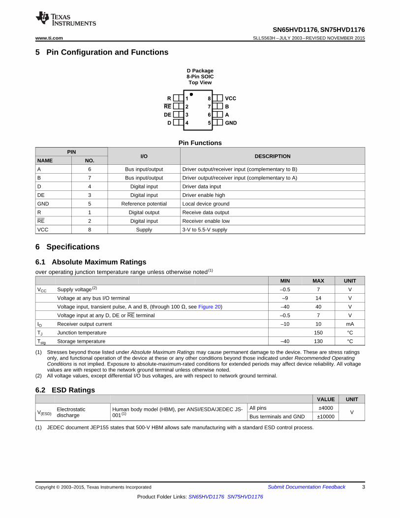
5 Pin Configuration and Functions
D Package8-Pin SOICTop View
Pin FunctionsPIN
I/O DESCRIPTIONNAME NO.A 6 Bus input/output Driver output/receiver input (complementary to B)B 7 Bus input/output Driver output/receiver input (complementary to A)D 4 Digital input Driver data inputDE 3 Digital input Driver enable highGND 5 Reference potential Local device groundR 1 Digital output Receive data outputRE 2 Digital input Receiver enable lowVCC 8 Supply 3-V to 5.5-V supply
6 Specifications
6.1 Absolute Maximum Ratingsover operating junction temperature range unless otherwise noted (1)
MIN MAX UNITVCC Supply voltage (2) –0.5 7 V
Voltage at any bus I/O terminal –9 14 VVoltage input, transient pulse, A and B, (through 100 Ω, see Figure 20) –40 40 VVoltage input at any D, DE or RE terminal –0.5 7 V
IO Receiver output current –10 10 mATJ Junction temperature 150 °CTstg Storage temperature –40 130 °C
(1) Stresses beyond those listed under Absolute Maximum Ratings may cause permanent damage to the device. These are stress ratingsonly, and functional operation of the device at these or any other conditions beyond those indicated under Recommended OperatingConditions is not implied. Exposure to absolute-maximum-rated conditions for extended periods may affect device reliability. All voltagevalues are with respect to the network ground terminal unless otherwise noted.
(2) All voltage values, except differential I/O bus voltages, are with respect to network ground terminal.
6.2 ESD RatingsVALUE UNIT
All pins ±4000Electrostatic Human body model (HBM), per ANSI/ESDA/JEDEC JS-V(ESD) Vdischarge 001 (1) Bus terminals and GND ±10000
(1) JEDEC document JEP155 states that 500-V HBM allows safe manufacturing with a standard ESD control process.
Copyright © 2003–2015, Texas Instruments Incorporated Submit Documentation Feedback 3
Product Folder Links: SN65HVD1176 SN75HVD1176
SN65HVD1176, SN75HVD1176SLLS563H –JULY 2003–REVISED NOVEMBER 2015 www.ti.com
6.3 Recommended Operating ConditionsMIN NOM MAX UNIT
VCC Supply voltage 4.75 5 5.25 VVoltage at either bus I/O terminal A, B –7 12 V
VIH High-level input voltage 2 VCC VD, DE, RE
VIL Low-level input voltage 0 0.8 VVIL Differential input voltage A with respect to B –12 12 V
Driver –70 70 mAIO Output current
Receiver –8 8 mASN65HVD1176 –40 130 °C
TJ Junction temperature (1)SN75HVD1176 0 130 °C
RL Differential load resistance 54 Ω1/tU1 Signaling rate 40 Mbps
(1) See the Power Dissipation table for more information on maintenance of this requirement.
6.4 Thermal InformationSN65HVD1176,SN75HVD1176
THERMAL METRIC (1) UNITD (SOIC)8 PINS
Low-K board (3), no air flow 208.3 °C/WRθJA Junction-to-ambient thermal resistance (2)
High-K board (4), no air flow 104.7 °C/WRθJC(top) Junction-to-case (top) thermal resistance 45.8 °C/WRθJB Junction-to-board thermal resistance High-K board 45.9 °C/WψJT Junction-to-top characterization parameter 5.7 °C/WψJB Junction-to-board characterization parameter 45.2 °C/W
(1) For more information about traditional and new thermal metrics, see the Semiconductor and IC Package Thermal Metrics applicationreport, SPRA953.
(2) The intent of RθJA specification is solely for a thermal performance comparison of one package to another in a standardizedenvironment. This methodology is not meant to and will not predict the performance of a package in an application-specific environment.
(3) JESD51-3, Low Effective Thermal Conductivity Test Board for Leaded Surface Mount Packages.(4) JESD51-7, High Effective Thermal Conductivity Test Board for Leaded Surface Mount Packages.
4 Submit Documentation Feedback Copyright © 2003–2015, Texas Instruments Incorporated
Product Folder Links: SN65HVD1176 SN75HVD1176
SN65HVD1176, SN75HVD1176www.ti.com SLLS563H –JULY 2003–REVISED NOVEMBER 2015
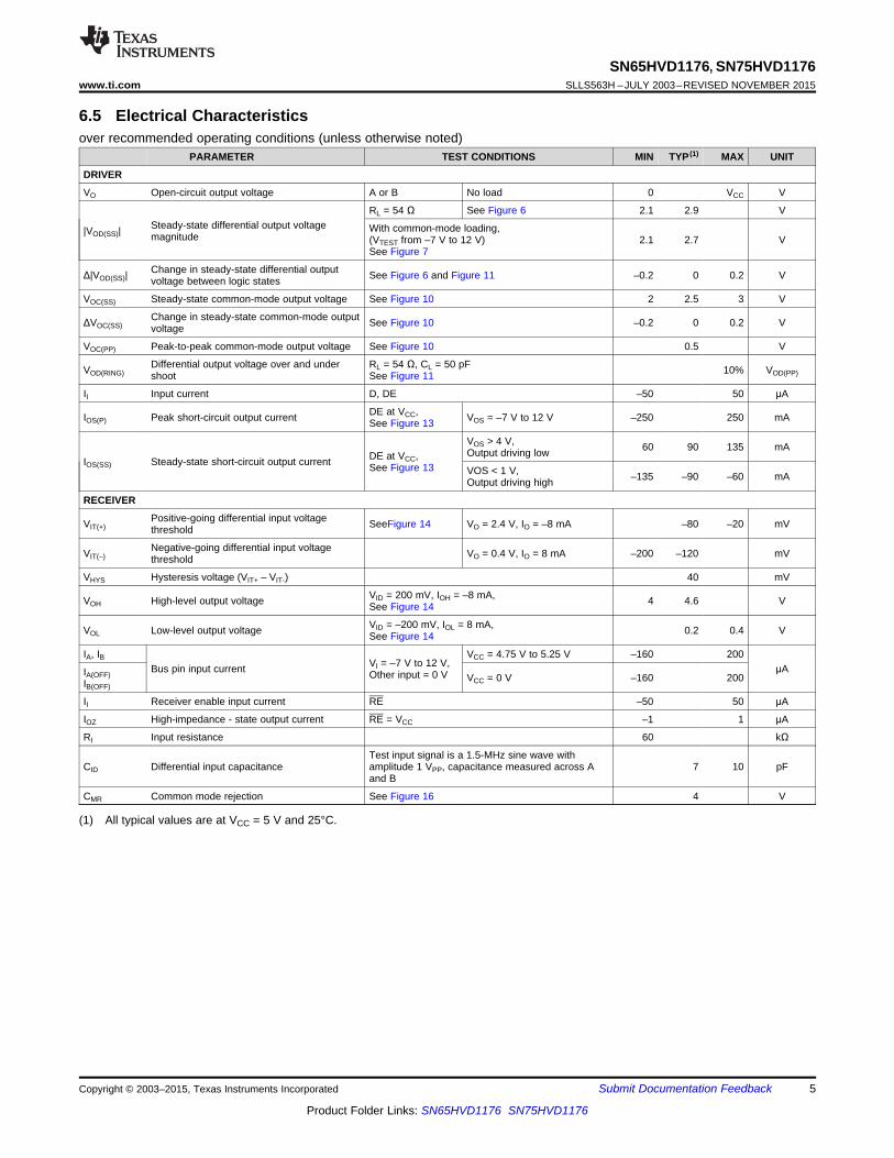
6.5 Electrical Characteristicsover recommended operating conditions (unless otherwise noted)
PARAMETER TEST CONDITIONS MIN TYP (1) MAX UNIT
DRIVER
VO Open-circuit output voltage A or B No load 0 VCC V
RL = 54 Ω See Figure 6 2.1 2.9 VSteady-state differential output voltage With common-mode loading,|VOD(SS)| magnitude (VTEST from –7 V to 12 V) 2.1 2.7 V
See Figure 7
Change in steady-state differential outputΔ|VOD(SS)| See Figure 6 and Figure 11 –0.2 0 0.2 Vvoltage between logic states
VOC(SS) Steady-state common-mode output voltage See Figure 10 2 2.5 3 V
Change in steady-state common-mode outputΔVOC(SS) See Figure 10 –0.2 0 0.2 Vvoltage
VOC(PP) Peak-to-peak common-mode output voltage See Figure 10 0.5 V
Differential output voltage over and under RL = 54 Ω, CL = 50 pFVOD(RING) 10% VOD(PP)shoot See Figure 11
II Input current D, DE –50 50 μA
DE at VCC,IOS(P) Peak short-circuit output current VOS = –7 V to 12 V –250 250 mASee Figure 13
VOS > 4 V, 60 90 135 mAOutput driving lowDE at VCC,IOS(SS) Steady-state short-circuit output current See Figure 13 VOS < 1 V, –135 –90 –60 mAOutput driving high
RECEIVER
Positive-going differential input voltageVIT(+) SeeFigure 14 VO = 2.4 V, IO = –8 mA –80 –20 mVthreshold
Negative-going differential input voltageVIT(–) VO = 0.4 V, IO = 8 mA –200 –120 mVthreshold
VHYS Hysteresis voltage (VIT+ – VIT-) 40 mV
VID = 200 mV, IOH = –8 mA,VOH High-level output voltage 4 4.6 VSee Figure 14
VID = –200 mV, IOL = 8 mA,VOL Low-level output voltage 0.2 0.4 VSee Figure 14
IA, IB VCC = 4.75 V to 5.25 V –160 200VI = –7 V to 12 V,Bus pin input current μAIA(OFF) Other input = 0 V VCC = 0 V –160 200IB(OFF)
II Receiver enable input current RE –50 50 μA
IOZ High-impedance - state output current RE = VCC –1 1 μA
RI Input resistance 60 kΩ
Test input signal is a 1.5-MHz sine wave withCID Differential input capacitance amplitude 1 VPP, capacitance measured across A 7 10 pF
and B
CMR Common mode rejection See Figure 16 4 V
(1) All typical values are at VCC = 5 V and 25°C.
Copyright © 2003–2015, Texas Instruments Incorporated Submit Documentation Feedback 5
Product Folder Links: SN65HVD1176 SN75HVD1176
SN65HVD1176, SN75HVD1176SLLS563H –JULY 2003–REVISED NOVEMBER 2015 www.ti.com
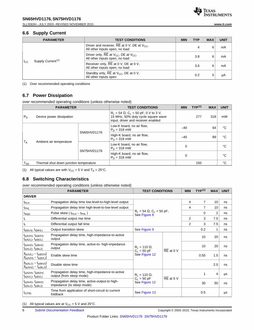
6.6 Supply CurrentPARAMETER TEST CONDITIONS MIN TYP MAX UNIT
Driver and receiver, RE at 0 V, DE at VCC, 4 6 mAAll other inputs open, no loadDriver only, RE at VCC, DE at VCC, 3.8 6 mAAll other inputs open, no load
ICC Supply Current (1)Receiver only, RE at 0 V, DE at 0 V, 3.6 6 mAAll other inputs open, no loadStandby only, RE at VCC, DE at 0 V, 0.2 5 μAAll other inputs open
(1) Over recommended operating conditions
6.7 Power Dissipationover recommended operating conditions (unless otherwise noted)
PARAMETER TEST CONDITIONS MIN TYP (1) MAX UNITRL = 54 Ω, CL = 50 pF, 0 V to 3 V,
PD Device power dissipation 15 MHz, 50% duty cycle square wave 277 318 mWinput, driver and receiver enabledLow-K board, no air flow, –40 64 °CPD = 318 mW
SN65HVD1176High-K board, no air flow, –40 89 °CPD = 318 mW
TA Ambient air temperatureLow-K board, no air flow, 0 °CPD = 318 mW
SN75HVD1176High-K board, no air flow, 0 °CPD = 318 mW
TSD Thermal shut down junction temperature 150 °C
(1) All typical values are with VCC = 5 V and TA = 25°C.
6.8 Switching Characteristicsover recommended operating conditions (unless otherwise noted)
PARAMETER TEST CONDITIONS MIN TYP (1) MAX UNITDRIVERtPLH Propagation delay time low-level-to-high-level output 4 7 10 nstPHL Propagation delay time high-level-to-low-level output 4 7 10 ns
RL = 54 Ω, CL = 50 pF,tsk(p) Pulse skew | tPLH – tPHL | 0 2 nsSee Figure 8tr Differential output rise time 2 3 7.5 nstf Differential output fall time 2 3 7.5 nstt(MLH), tt(MHL) Output transition skew See Figure 9 0.2 1 nstp(AZH), tp(BZH) Propagation delay time, high-impedance-to-active 10 20 nstp(AZL), tp(BZL) outputtp(AHZ), tp(BHZ) Propagation delay time, active-to- high-impedance 10 20 nsRL = 110 Ω,tp(ALZ), tp(BLZ) output
CL = 50 pF RE at 0 V|tp(AZL) – tp(BZH)| See Figure 12Enable skew time 0.55 1.5 ns|tp(AZH) – tp(BZL)||tp(ALZ) – tp(BHZ)| Disable skew time 2.5 ns|tp(AHZ) – tp(BLZ)|tp(AZH), tp(BZH) Propagation delay time, high-impedance-to-active 1 4 μsRL = 110 Ω,tp(AZL), tp(BZL) output (from sleep mode)
CL = 50 pF RE at 5 Vtp(AHZ), tp(BHZ) Propagation delay time, active-output-to high- See Figure 12 30 50 nstp(ALZ), tp(BLZ) impedance (to sleep mode)
Time from application of short-circuit to currentt(CFB) See Figure 13 0.5 μsfoldback
(1) All typical values are at VCC = 5 V and 25°C.
6 Submit Documentation Feedback Copyright © 2003–2015, Texas Instruments Incorporated
Product Folder Links: SN65HVD1176 SN75HVD1176

SN65HVD1176, SN75HVD1176www.ti.com SLLS563H –JULY 2003–REVISED NOVEMBER 2015
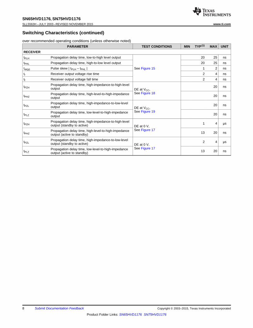
Switching Characteristics (continued)over recommended operating conditions (unless otherwise noted)
PARAMETER TEST CONDITIONS MIN TYP (1) MAX UNITTime from application of short-circuit to thermal TA = 25°C,t(TSD) 100 μsshutdown See Figure 13
Copyright © 2003–2015, Texas Instruments Incorporated Submit Documentation Feedback 7
Product Folder Links: SN65HVD1176 SN75HVD1176
SN65HVD1176, SN75HVD1176SLLS563H –JULY 2003–REVISED NOVEMBER 2015 www.ti.com
Switching Characteristics (continued)over recommended operating conditions (unless otherwise noted)
PARAMETER TEST CONDITIONS MIN TYP (1) MAX UNITRECEIVERtPLH Propagation delay time, low-to-high level output 20 25 nstPHL Propagation delay time, high-to-low level output 20 25 nstsk(p) Pulse skew | tPLH – tPHL | See Figure 15 1 2 nstr Receiver output voltage rise time 2 4 nstf Receiver output voltage fall time 2 4 ns
Propagation delay time, high-impedance-to-high-leveltPZH 20 nsoutput DE at VCC,See Figure 18Propagation delay time, high-level-to-high-impedancetPHZ 20 nsoutput
Propagation delay time, high-impedance-to-low-leveltPZL 20 nsoutput DE at VCC,See Figure 19Propagation delay time, low-level-to-high-impedancetPLZ 20 nsoutput
Propagation delay time, high-impedance-to-high-leveltPZH 1 4 μsoutput (standby to active) DE at 0 V,See Figure 17Propagation delay time, high-level-to-high-impedancetPHZ 13 20 nsoutput (active to standby)
Propagation delay time, high-impedance-to-low-leveltPZL 2 4 μsoutput (standby to active) DE at 0 V,See Figure 17Propagation delay time, low-level-to-high-impedancetPLZ 13 20 nsoutput (active to standby)
8 Submit Documentation Feedback Copyright © 2003–2015, Texas Instruments Incorporated
Product Folder Links: SN65HVD1176 SN75HVD1176

0
0.1
0.2
0.3
0.4
0.5
0.6
0.7
−40 −15 10 35 60 85
VCC = 4.75 V
VCC = 5.25 V
TA − Free-Air Temperature −°C
Dri
ver
En
ab
le S
kew
−n
s
RL = 110 Ω,
CL = 50 pF
VCC = 5 V
0
0.05
0.1
0.15
0.2
0.25
0.3
0.35
−40 −15 10 35 60 85
VCC = 4.75 V
VCC = 5 V
VCC = 5.25 V
Dri
ve
r O
utp
ut
Tra
ns
itio
n S
ke
w−
ns
TA − Free-Air Temperature −°C
RL = 54 Ω,
CL = 50 pF
2
2.25
2.5
2.75
3
3.25
3.5
3.75
4
−40 −15 10 35 60 85
VCC = 4.75 V
VCC = 5.25 V
VCC = 5 VD
river
Ris
e, F
all T
ime
−n
s
TA − Free-Air Temperature −°C
RL = 54 Ω,
CL = 50 pF
0
0.5
1
1.5
2
2.5
3
3.5
4
4.5
5
0 20 40 60 80
VCC = 4.75 V
VCC = 5 V
VCC = 5.25 V
VO
D−
Dif
fere
nti
al O
utp
ut
Volt
ag
e−
V
IL − Load Current − mA
100 Ω
50 Ω
TA = 25 C54
56
58
60
62
64
66
0 10 20 30 40 50
Signaling Rate − Mbps
ID
D−
Dri
ve
r S
up
ply
Cu
rre
nt
−m
Arm
s
VCC = 5 V
TA = 25°C
RL = 56 Ω,
DE and RE at 5 V
Input 0 V to 3 V PRBS
SN65HVD1176, SN75HVD1176www.ti.com SLLS563H –JULY 2003–REVISED NOVEMBER 2015
6.9 Typical Characteristics
Figure 1. Differential Output Voltage vs Load Current Figure 2. Driver Supply Current vs Signaling Rate
Figure 3. Driver Output Transition Skew vs Free-Air Figure 4. Driver Rise, Fall Time vs Free-Air TemperatureTemperature
Figure 5. Driver Enable Skew vs Free-Air Temperature
Copyright © 2003–2015, Texas Instruments Incorporated Submit Documentation Feedback 9
Product Folder Links: SN65HVD1176 SN75HVD1176

VOD
50 Ω
RL = 54 Ω
CL = 50 pFSignal
Generator
3 V
0 V
VOD(H)
VOD(L)
90%
10%
tr tf
INPUT
OUTPUT
VOD 60 Ω
VTEST
0 V or 3 V
375 Ω
375 Ω
VTEST = −7 V to 12 V
A
B
D
IIIO
IO
VOD 50 pF
27 Ω
27 Ω
VOC
0 V or 3 V
A
B
D
SN65HVD1176, SN75HVD1176SLLS563H –JULY 2003–REVISED NOVEMBER 2015 www.ti.com
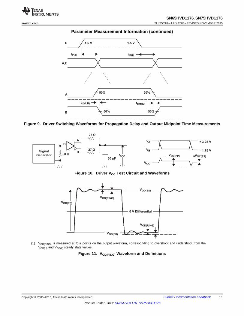
7 Parameter Measurement Information
NOTETest load capacitance includes probe and jig capacitance (unless otherwise specified).
Signal generator characteristics: rise and fall time < 6 ns, pulse rate 100 kHz, 50% dutycycle, Zo = 50 Ω (unless otherwise specified).
Figure 6. Driver Test Circuit, VOD and VOC Without Common-Mode Loading
Figure 7. Driver Test Circuit, VOD With Common-Mode Loading
Figure 8. Driver Switching Test Circuit and Rise/Fall Time Measurement
10 Submit Documentation Feedback Copyright © 2003–2015, Texas Instruments Incorporated
Product Folder Links: SN65HVD1176 SN75HVD1176
VOD(PP)
VOD(RING)
VOD(RING)
VOD(SS)
VOD(SS)
0 V Differential
VOC50 Ω
Signal
Generator
A
B
27 Ω
27 Ω
50 pF
DVA
VB
VOC
VOC(PP) ∆VOC(SS)
≈ 3.25 V
≈ 1.75 V
tPLH tPHL
1.5 V 1.5 V
50% 50%
50% 50%
tt(MLH) tt(MHL)
D
A,B
A
B
SN65HVD1176, SN75HVD1176www.ti.com SLLS563H –JULY 2003–REVISED NOVEMBER 2015
Parameter Measurement Information (continued)
Figure 9. Driver Switching Waveforms for Propagation Delay and Output Midpoint Time Measurements
Figure 10. Driver VOC Test Circuit and Waveforms
(1) VOD(RING) is measured at four points on the output waveform, corresponding to overshoot and undershoot from theVOD(H) and VOD(L) steady state values.
Figure 11. VOD(RING) Waveform and Definitions
Copyright © 2003–2015, Texas Instruments Incorporated Submit Documentation Feedback 11
Product Folder Links: SN65HVD1176 SN75HVD1176

VID
VA
VB
IOA
B
IB VO
R
IA
VICVA + VB
2
60
250
135
IOS
Voltage
Source
VOS
Output
Current |mA|
t(CFB)
t(TSD)
time
D
a) D at Logic Low
b) D at Logic High
DE
A
B
tp(AZL) tp(ALZ)
tp(BZH)tp(BHZ)
A
B
CL = 50 pF
RL = 110 Ω
0 V
DE
D
Signal
Generator 50 Ω CL = 50 pF
RL = 110 ΩVCC
0 V
50%
50%
1.5 V
VOL +0.5 V
VOL −0.5 V
DE
A
B
tp(AZH) tp(AHZ)
tp(BZL)tp(BLZ)
A
B
CL = 50 pF
RL = 110 Ω
3 V
DE
D
Signal
Generator50 Ω CL = 50 pF
RL = 110 Ω
VCC
0 V
50%
50%
1.5 V
VOH −0.5 V
VOH +0.5 V
1.5 V
3 V
3 V
SN65HVD1176, SN75HVD1176SLLS563H –JULY 2003–REVISED NOVEMBER 2015 www.ti.com
Parameter Measurement Information (continued)
Figure 12. Driver Enable/Disable Test
Figure 13. Driver Short-Circuit Test Circuit and Waveforms (Short Circuit applied at Time t = 0)
Figure 14. Receiver DC Parameter Definitions
12 Submit Documentation Feedback Copyright © 2003–2015, Texas Instruments Incorporated
Product Folder Links: SN65HVD1176 SN75HVD1176

VI = A sin 2 ft
1 MHz < f < 50 MHz
100 nF
2.2 kΩ
Voffset =
−2 V to 7 V
50 Ω
50 Ω470 nF
RE
R
DE
D
ScopeVR2.2 kΩ
VCC
100 nF
GND
A
B
Scope
VR shall be greater than
2 V throughout this test.
50 ΩSignal
Generator
CL = 15 pF50 Ω
Signal
Generator
A
VID
BR
IO
VO
50%
90%
10%
1.5 V
0 V
VOH
VOL
tPLH tPHL
tr tf
Input B
Input A
Output 1.5 V
SN65HVD1176, SN75HVD1176www.ti.com SLLS563H –JULY 2003–REVISED NOVEMBER 2015
Parameter Measurement Information (continued)
Figure 15. Receiver Switching Test Circuit and Waveforms
Figure 16. Receiver Common-Mode Rejection Test Circuit
Copyright © 2003–2015, Texas Instruments Incorporated Submit Documentation Feedback 13
Product Folder Links: SN65HVD1176 SN75HVD1176

50 ΩSignal
Generator
RE
B
A
54 Ω
CL = 15 pF
R 1 kΩ0 V
VCC
VCC
D
DE
RE
R
1.5 V
tPZH tPHZ
3 V
0 V
VOH
VOH −0.5 V
GND
1.5 V
Input
Generator 50 Ω
VO
RE
RA
B
3 V
1.5 V
tPZH(2)
1.5 V
3 V
0 V
VOH
GND
VI
VO
0 V or 1.5 V
1.5 V or 0 V CL = 15 pF ±20%
VI
1 kΩ ± 1%A
B
S1
A at 1.5 V
B at 0 V
S1 to B
tPZL(2)
1.5 V
3 V
VOL
VO
A at 0 V
B at 1.5 V
S1 to A
SN65HVD1176, SN75HVD1176SLLS563H –JULY 2003–REVISED NOVEMBER 2015 www.ti.com
Parameter Measurement Information (continued)
Figure 17. Receiver Enable Time From Standby (Driver Disabled)
Figure 18. Receiver Enable Test Circuit and Waveforms, Data Output High (Driver Active)
14 Submit Documentation Feedback Copyright © 2003–2015, Texas Instruments Incorporated
Product Folder Links: SN65HVD1176 SN75HVD1176

Pulse Generator,
15 ms Duration,
1% Duty Cycle
100 ΩVTEST
0 V
15 ms 1.5 ms −VTEST
1 kΩ
Ω
Ω
SN65HVD1176, SN75HVD1176www.ti.com SLLS563H –JULY 2003–REVISED NOVEMBER 2015
Parameter Measurement Information (continued)
Figure 19. Receiver Enable Test Circuit and Waveforms, Data Output Low (Driver Active)
Figure 20. Test Circuit and Waveforms, Transient Overvoltage Test
Copyright © 2003–2015, Texas Instruments Incorporated Submit Documentation Feedback 15
Product Folder Links: SN65HVD1176 SN75HVD1176

R
D
DE
RE
B
A
GND
VCC
SN65HVD1176, SN75HVD1176SLLS563H –JULY 2003–REVISED NOVEMBER 2015 www.ti.com
8 Detailed Description
8.1 OverviewThe SNx5HVD1176 device is a 5-V, half-duplex, RS-485 transceiver optimized for use in PROFIBUS (EN50170)applications and suitable for data transmission up to 40 Mbps.
The driver output differential voltage exceeds the PROFIBUS requirement of 2.1 V with a 54-Ω load, and the lowtransceiver output capacitance of 10 pF supports the PROFIBUS requirements for maximum bus capacitanceacross various data rates.
This device has an active-high driver enable and an active-low receiver enable. A standby current of less than5 µA can be achieved by disabling both driver and receiver.
8.2 Functional Block Diagram
Figure 21. Logic Diagram (Positive Logic)
8.3 Feature DescriptionInternal ESD protection circuits protect the transceiver bus terminals against ±10-kV Human Body Model (HBM)electrostatic discharges and all other pins up to ±4 kV.
The SN65HVD1176 device provides internal biasing of the receiver input thresholds for open-circuit, bus-idle, orshort-circuit failsafe conditions, and a typical receiver hysteresis of 40 mV.
8.4 Device Functional Modes
Table 1. Driver Function Table (1)
INPUT ENABLE OUTPUTSD DE A BH H H LL H L HX L Z ZX OPEN Z Z
OPEN H H L
(1) H = high level, L = low level, X = don’t care,Z = high impedance (off)
16 Submit Documentation Feedback Copyright © 2003–2015, Texas Instruments Incorporated
Product Folder Links: SN65HVD1176 SN75HVD1176

9 V
500 Ω
200 kΩ
Input
VCC
D and RE Inputs
9 V
500 Ω
200 kΩ
Input
VCC
DE Input
16 V
16 V
90 kΩ
18 kΩ
Input
A Input
16 V
16 V
Input
B Input
16 V
16 V
VCC
A and B Outputs
9 V
VCC
R Output
5 ΩOutput
VCCVCC
Output
18 kΩ 18 kΩ
18 kΩ
90 kΩ
SN65HVD1176, SN75HVD1176www.ti.com SLLS563H –JULY 2003–REVISED NOVEMBER 2015
Table 2. Receiver Function Table (1)
DIFFRENTIAL INPUT ENABLE OUTPUTVID = (VA – VB) RE RVID ≥ –0.02 V L H
–0.2 V < VID < –0.02 V L ?VID ≤ –0.2 V L L
X H ZX OPEN Z
Open Circuit L HShort Circuit L H
Idle (terminated) bus L H
(1) H = high level, L = low level, X = don’t care,Z = high impedance (off), ? = indeterminate
Figure 22. Equivalent Input and Output Schematic Diagrams
Copyright © 2003–2015, Texas Instruments Incorporated Submit Documentation Feedback 17
Product Folder Links: SN65HVD1176 SN75HVD1176
RT RT
R
A B
R RE DE D
DR
A B
R RE DE D
D
R
D
R
RE
DE
D
A
B
R
D
R
RE
DE
D
A
B
R
D
R
RE
DE
D
A
B
R
D
R
RE
DE
D
A
B
R
D
R
RE
DE
D
A
B
SN65HVD1176, SN75HVD1176SLLS563H –JULY 2003–REVISED NOVEMBER 2015 www.ti.com
9 Application and Implementation
NOTEInformation in the following applications sections is not part of the TI componentspecification, and TI does not warrant its accuracy or completeness. TI’s customers areresponsible for determining suitability of components for their purposes. Customers shouldvalidate and test their design implementation to confirm system functionality.
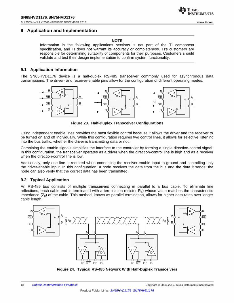
9.1 Application InformationThe SN65HVD1176 device is a half-duplex RS-485 transceiver commonly used for asynchronous datatransmissions. The driver- and receiver-enable pins allow for the configuration of different operating modes.
Figure 23. Half-Duplex Transceiver Configurations
Using independent enable lines provides the most flexible control because it allows the driver and the receiver tobe turned on and off individually. While this configuration requires two control lines, it allows for selective listeninginto the bus traffic, whether the driver is transmitting data or not.
Combining the enable signals simplifies the interface to the controller by forming a single direction-control signal.In this configuration, the transceiver operates as a driver when the direction-control line is high and as a receiverwhen the direction-control line is low.
Additionally, only one line is required when connecting the receiver-enable input to ground and controlling onlythe driver-enable input. In this configuration, a node receives the data from the bus and the data it sends; thenode can also verify that the correct data has been transmitted.
9.2 Typical ApplicationAn RS-485 bus consists of multiple transceivers connecting in parallel to a bus cable. To eliminate linereflections, each cable end is terminated with a termination resistor RT) whose value matches the characteristicimpedance (Z0) of the cable. This method, known as parallel termination, allows for higher data rates over longercable length.
Figure 24. Typical RS-485 Network With Half-Duplex Transceivers
18 Submit Documentation Feedback Copyright © 2003–2015, Texas Instruments Incorporated
Product Folder Links: SN65HVD1176 SN75HVD1176
10000
1000
100
10
Cab
le L
en
gth
(ft
)
100 1k 10k 100k 1M 10M 100M
Data Rate (bps)
Conservative
Characteristics
5%, 10%, and 20% Jitter
220Ω
R
A B
R RE DE D
DR
A B
R RE DE D
D
R
D
R
RE
DE
D
A
B
R
D
R
RE
DE
D
A
B220Ω
5V
390Ω
390Ω
5V
390Ω
390Ω
SN65HVD1176, SN75HVD1176www.ti.com SLLS563H –JULY 2003–REVISED NOVEMBER 2015
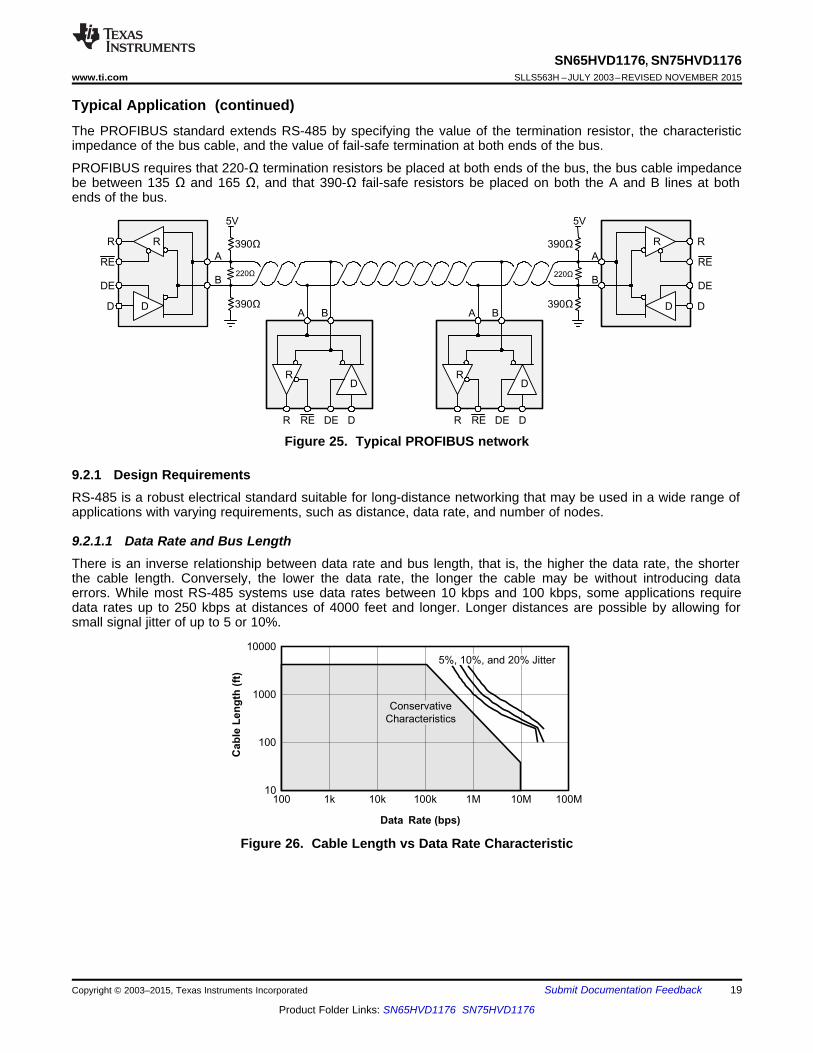
Typical Application (continued)The PROFIBUS standard extends RS-485 by specifying the value of the termination resistor, the characteristicimpedance of the bus cable, and the value of fail-safe termination at both ends of the bus.
PROFIBUS requires that 220-Ω termination resistors be placed at both ends of the bus, the bus cable impedancebe between 135 Ω and 165 Ω, and that 390-Ω fail-safe resistors be placed on both the A and B lines at bothends of the bus.
Figure 25. Typical PROFIBUS network
9.2.1 Design RequirementsRS-485 is a robust electrical standard suitable for long-distance networking that may be used in a wide range ofapplications with varying requirements, such as distance, data rate, and number of nodes.
9.2.1.1 Data Rate and Bus LengthThere is an inverse relationship between data rate and bus length, that is, the higher the data rate, the shorterthe cable length. Conversely, the lower the data rate, the longer the cable may be without introducing dataerrors. While most RS-485 systems use data rates between 10 kbps and 100 kbps, some applications requiredata rates up to 250 kbps at distances of 4000 feet and longer. Longer distances are possible by allowing forsmall signal jitter of up to 5 or 10%.
Figure 26. Cable Length vs Data Rate Characteristic
Copyright © 2003–2015, Texas Instruments Incorporated Submit Documentation Feedback 19
Product Folder Links: SN65HVD1176 SN75HVD1176

SN65HVD1176, SN75HVD1176SLLS563H –JULY 2003–REVISED NOVEMBER 2015 www.ti.com
Typical Application (continued)9.2.1.2 Stub LengthWhen connecting a node to the bus, the distance between the transceiver inputs and the cable trunk, known asthe stub, should be as short as possible. Stubs present a nonterminated piece of bus line which can introducereflections as the length of the stub increases. As a general guideline, the electrical length, or round-trip delay, ofa stub should be less than one-tenth of the rise time of the driver, thus giving a maximum physical stub length asshown in Equation 1.
Lstub ≤ 0.1 × tr × v × c (1)
where:tr is the 10/90 rise time of the driverc is the speed of light (3 × 10⁸ m/s)v is the signal velocity of the cable or trace as a factor of c
Per Equation 1, the maximum recommended stub length for the minimum driver output rise time of theSN65HVD1176 device for a signal velocity of 78% is 0.05 meters (0.16 feet).
9.2.1.3 Bus LoadingThe RS-485 standard specifies that a compliant driver must be able to driver 32 unit loads (UL), where 1 unitload represents a load impedance of approximately 12 kΩ. Because the SN65HVD1176 device is a 1/5 ULtransceiver, it is possible to connect up to 160 receivers to the bus.
9.2.1.4 Receiver FailsafeThe differential receiver of the SN65HVD1176 device is failsafe to invalid bus states caused by the following:• Open bus conditions, such as a disconnected connector• Shorted bus conditions, such as cable damage shorting the twisted-pair together• Idle bus conditions that occur when no driver on the bus is actively driving
In any of these cases, the differential receiver will output a failsafe logic-high state so that the output of thereceiver is not indeterminate.
Receiver failsafe is accomplished by offsetting the receiver thresholds such that the input-indeterminate rangedoes not include zero volts differential.
To comply with the RS-422 and RS-485 standards, the receiver output must output a high when the differentialinput VID is more positive than +200 mV, and must output a low when VID is more negative than –200 mV. Thereceiver parameters that determine the fail-safe performance are VIT(+) and VIT(–).
As shown in Electrical Characteristics, differential signals more negative than –200 mV will always cause a lowreceiver output, and differential signals more positive than –20 mV will always cause a high receiver output.Thus, when the differential input signal is close to zero, it is still above the maximum VIT(+) threshold of –20 mV,and the receiver output will be high.
20 Submit Documentation Feedback Copyright © 2003–2015, Texas Instruments Incorporated
Product Folder Links: SN65HVD1176 SN75HVD1176

5V
VCC
GND
D
DE
R
RE
B
A
RxD
TxD
DIR
MCU/
UART
10k
10k
TVS
R2
R1
HVD1176
100nF100nF
SN65HVD1176, SN75HVD1176www.ti.com SLLS563H –JULY 2003–REVISED NOVEMBER 2015
Typical Application (continued)9.2.2 Detailed Design ProcedureTo protect bus nodes against high-energy transients, the implementation of external transient protection devicesis necessary.
Figure 27. Transient Protection Against ESD, EFT, and Surge Transients
Figure 27 shows a protection circuit against 10-kV ESD (IEC 61000-4-2), 4-kV EFT (IEC 61000-4-4), and 1-kVsurge (IEC 61000-4-5) transients. Table 3 lists the associated Bill of Materials.
Table 3. Bill of MaterialsDevice Function Order Number ManufacturerXCVR 5-V, 40-Mbps ProfiBus Transceiver SN65HVD1176 TIR1, R2 10-Ω, Pulse-Proof Thick-Film Resistor CRCW0603010RJNEAHP Vishay
TVS Bidirectional 400-W Transient Suppressor CDSOT23-SM712 Bourns
9.2.3 Application CurveFigure 28 demonstrates operation of the SN65HVD1179 at a signaling rate of 40 Mbps.
Figure 28. Differential Output of SN65HVD1176 Operation at 40 Mbps
Copyright © 2003–2015, Texas Instruments Incorporated Submit Documentation Feedback 21
Product Folder Links: SN65HVD1176 SN75HVD1176
MCU
R
R
Via to ground
SN65HVD1176
JM
P
R
R
R
C
5
6
6
1
4R
5
Via to VCC
TVS
75
SN65HVD1176, SN75HVD1176SLLS563H –JULY 2003–REVISED NOVEMBER 2015 www.ti.com
10 Power Supply RecommendationsTo ensure reliable operation at all data rates and supply voltages, each supply must be buffered with a 100-nFceramic capacitor located as close to the supply pins as possible. The TPS76350 device is a linear voltageregulator suitable for the 5-V supply.
11 Layout
11.1 Layout GuidelinesOn-chip IEC-ESD protection is sufficient for laboratory and portable equipment but insufficient for EFT and surgetransients occurring in industrial environments. Therefore, robust and reliable bus-node design requires the useof external transient protection devices.
Because ESD and EFT transients have a wide frequency bandwidth from approximately 3 MHz to 3 GHz, highfrequency layout techniques must be applied during PCB design.1. Place the protection circuitry close to the bus connector to prevent noise transients from entering the board.2. Use VCC and ground planes to provide low-inductance.3. Design the protection components into the direction of the signal path. Do not force the transient currents to
divert from the signal path to reach the protection device.4. Apply 100-nF to 220-nF bypass capacitors as close as possible to the VCC pins of the transceiver, the
UART, or the controller ICs on the board.5. Use at least two vias for VCC and ground connections of bypass capacitors and protection devices to
minimize effective via inductance.6. Use 1-kΩ to 10-kΩ pullup and pulldown resistors for enable lines to limit noise currents in these lines during
transient events.7. Insert series pulse-proof resistors into the A and B bus lines if the TVS clamping voltage is higher than the
specified maximum voltage of the transceiver bus terminals. These resistors limit the residual clampingcurrent into the transceiver and prevent it from latching up.
8. While pure TVS protection is sufficient for surge transients up to 1 kV, higher transients require metal-oxidevaristors (MOVs) that reduce the transients to a few hundred volts of clamping voltage and transient blockingunits (TBUs) that limit transient current to less than 1 mA.
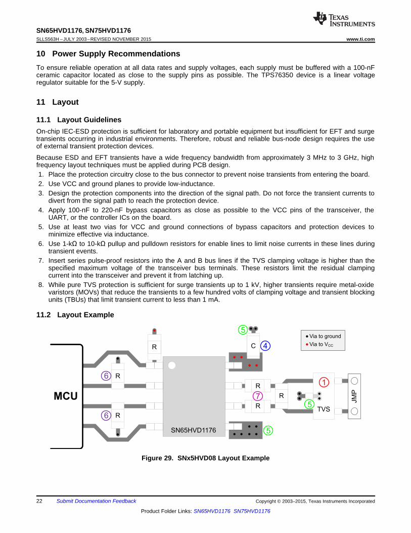
11.2 Layout Example
Figure 29. SNx5HVD08 Layout Example
22 Submit Documentation Feedback Copyright © 2003–2015, Texas Instruments Incorporated
Product Folder Links: SN65HVD1176 SN75HVD1176
SN65HVD1176, SN75HVD1176www.ti.com SLLS563H –JULY 2003–REVISED NOVEMBER 2015
12 Device and Documentation Support
12.1 Third-Party Products DisclaimerTI'S PUBLICATION OF INFORMATION REGARDING THIRD-PARTY PRODUCTS OR SERVICES DOES NOTCONSTITUTE AN ENDORSEMENT REGARDING THE SUITABILITY OF SUCH PRODUCTS OR SERVICESOR A WARRANTY, REPRESENTATION OR ENDORSEMENT OF SUCH PRODUCTS OR SERVICES, EITHERALONE OR IN COMBINATION WITH ANY TI PRODUCT OR SERVICE.
12.2 Documentation SupportFor related documentation see the following: ISO1176 ISOLATED RS-485 PROFIBUS TRANSCEIVER(SLLS897)
12.3 Related LinksThe table below lists quick access links. Categories include technical documents, support and communityresources, tools and software, and quick access to sample or buy.
Table 4. Related LinksTECHNICAL TOOLS & SUPPORT &PARTS PRODUCT FOLDER SAMPLE & BUY DOCUMENTS SOFTWARE COMMUNITY
SN65HVD1176 Click here Click here Click here Click here Click hereSN75HVD1176 Click here Click here Click here Click here Click here
12.4 Community ResourcesThe following links connect to TI community resources. Linked contents are provided "AS IS" by the respectivecontributors. They do not constitute TI specifications and do not necessarily reflect TI's views; see TI's Terms ofUse.
TI E2E™ Online Community TI's Engineer-to-Engineer (E2E) Community. Created to foster collaborationamong engineers. At e2e.ti.com, you can ask questions, share knowledge, explore ideas and helpsolve problems with fellow engineers.
Design Support TI's Design Support Quickly find helpful E2E forums along with design support tools andcontact information for technical support.
12.5 TrademarksE2E is a trademark of Texas Instruments.PROFIBUS is a registered trademark of PROFIBUS Nutzerorganisation e.V..All other trademarks are the property of their respective owners.
12.6 Electrostatic Discharge CautionThese devices have limited built-in ESD protection. The leads should be shorted together or the device placed in conductive foamduring storage or handling to prevent electrostatic damage to the MOS gates.
12.7 GlossarySLYZ022 — TI Glossary.
This glossary lists and explains terms, acronyms, and definitions.
13 Mechanical, Packaging, and Orderable InformationThe following pages include mechanical, packaging, and orderable information. This information is the mostcurrent data available for the designated devices. This data is subject to change without notice and revision ofthis document. For browser-based versions of this data sheet, refer to the left-hand navigation.
Copyright © 2003–2015, Texas Instruments Incorporated Submit Documentation Feedback 23
Product Folder Links: SN65HVD1176 SN75HVD1176

PACKAGE OPTION ADDENDUM
www.ti.com 24-Aug-2018
Addendum-Page 1
PACKAGING INFORMATION
Orderable Device Status(1)
Package Type PackageDrawing
Pins PackageQty
Eco Plan(2)
Lead/Ball Finish(6)
MSL Peak Temp(3)
Op Temp (°C) Device Marking(4/5)
Samples
SN65HVD1176D ACTIVE SOIC D 8 75 Green (RoHS& no Sb/Br)
CU NIPDAU Level-1-260C-UNLIM -40 to 85 VP1176
SN65HVD1176DG4 ACTIVE SOIC D 8 75 Green (RoHS& no Sb/Br)
CU NIPDAU Level-1-260C-UNLIM -40 to 85 VP1176
SN65HVD1176DR ACTIVE SOIC D 8 2500 Green (RoHS& no Sb/Br)
CU NIPDAU Level-1-260C-UNLIM -40 to 85 VP1176
SN65HVD1176DRG4 ACTIVE SOIC D 8 2500 Green (RoHS& no Sb/Br)
CU NIPDAU Level-1-260C-UNLIM -40 to 85 VP1176
SN75HVD1176D ACTIVE SOIC D 8 75 Green (RoHS& no Sb/Br)
CU NIPDAU Level-1-260C-UNLIM 0 to 70 VN1176
SN75HVD1176DR ACTIVE SOIC D 8 2500 Green (RoHS& no Sb/Br)
CU NIPDAU Level-1-260C-UNLIM 0 to 70 VN1176
SN75HVD1176DRG4 ACTIVE SOIC D 8 2500 Green (RoHS& no Sb/Br)
CU NIPDAU Level-1-260C-UNLIM 0 to 70 VN1176
(1) The marketing status values are defined as follows:ACTIVE: Product device recommended for new designs.LIFEBUY: TI has announced that the device will be discontinued, and a lifetime-buy period is in effect.NRND: Not recommended for new designs. Device is in production to support existing customers, but TI does not recommend using this part in a new design.PREVIEW: Device has been announced but is not in production. Samples may or may not be available.OBSOLETE: TI has discontinued the production of the device.
(2) RoHS: TI defines "RoHS" to mean semiconductor products that are compliant with the current EU RoHS requirements for all 10 RoHS substances, including the requirement that RoHS substancedo not exceed 0.1% by weight in homogeneous materials. Where designed to be soldered at high temperatures, "RoHS" products are suitable for use in specified lead-free processes. TI mayreference these types of products as "Pb-Free".RoHS Exempt: TI defines "RoHS Exempt" to mean products that contain lead but are compliant with EU RoHS pursuant to a specific EU RoHS exemption.Green: TI defines "Green" to mean the content of Chlorine (Cl) and Bromine (Br) based flame retardants meet JS709B low halogen requirements of <=1000ppm threshold. Antimony trioxide basedflame retardants must also meet the <=1000ppm threshold requirement.
(3) MSL, Peak Temp. - The Moisture Sensitivity Level rating according to the JEDEC industry standard classifications, and peak solder temperature.
(4) There may be additional marking, which relates to the logo, the lot trace code information, or the environmental category on the device.
(5) Multiple Device Markings will be inside parentheses. Only one Device Marking contained in parentheses and separated by a "~" will appear on a device. If a line is indented then it is a continuationof the previous line and the two combined represent the entire Device Marking for that device.

PACKAGE OPTION ADDENDUM
www.ti.com 24-Aug-2018
Addendum-Page 2
(6) Lead/Ball Finish - Orderable Devices may have multiple material finish options. Finish options are separated by a vertical ruled line. Lead/Ball Finish values may wrap to two lines if the finishvalue exceeds the maximum column width.
Important Information and Disclaimer:The information provided on this page represents TI's knowledge and belief as of the date that it is provided. TI bases its knowledge and belief on informationprovided by third parties, and makes no representation or warranty as to the accuracy of such information. Efforts are underway to better integrate information from third parties. TI has taken andcontinues to take reasonable steps to provide representative and accurate information but may not have conducted destructive testing or chemical analysis on incoming materials and chemicals.TI and TI suppliers consider certain information to be proprietary, and thus CAS numbers and other limited information may not be available for release.
In no event shall TI's liability arising out of such information exceed the total purchase price of the TI part(s) at issue in this document sold by TI to Customer on an annual basis.

TAPE AND REEL INFORMATION
*All dimensions are nominal
Device PackageType
PackageDrawing
Pins SPQ ReelDiameter
(mm)
ReelWidth
W1 (mm)
A0(mm)
B0(mm)
K0(mm)
P1(mm)
W(mm)
Pin1Quadrant
SN65HVD1176DR SOIC D 8 2500 330.0 12.4 6.4 5.2 2.1 8.0 12.0 Q1
SN75HVD1176DR SOIC D 8 2500 330.0 12.4 6.4 5.2 2.1 8.0 12.0 Q1
PACKAGE MATERIALS INFORMATION
www.ti.com 23-Sep-2015
Pack Materials-Page 1
*All dimensions are nominal
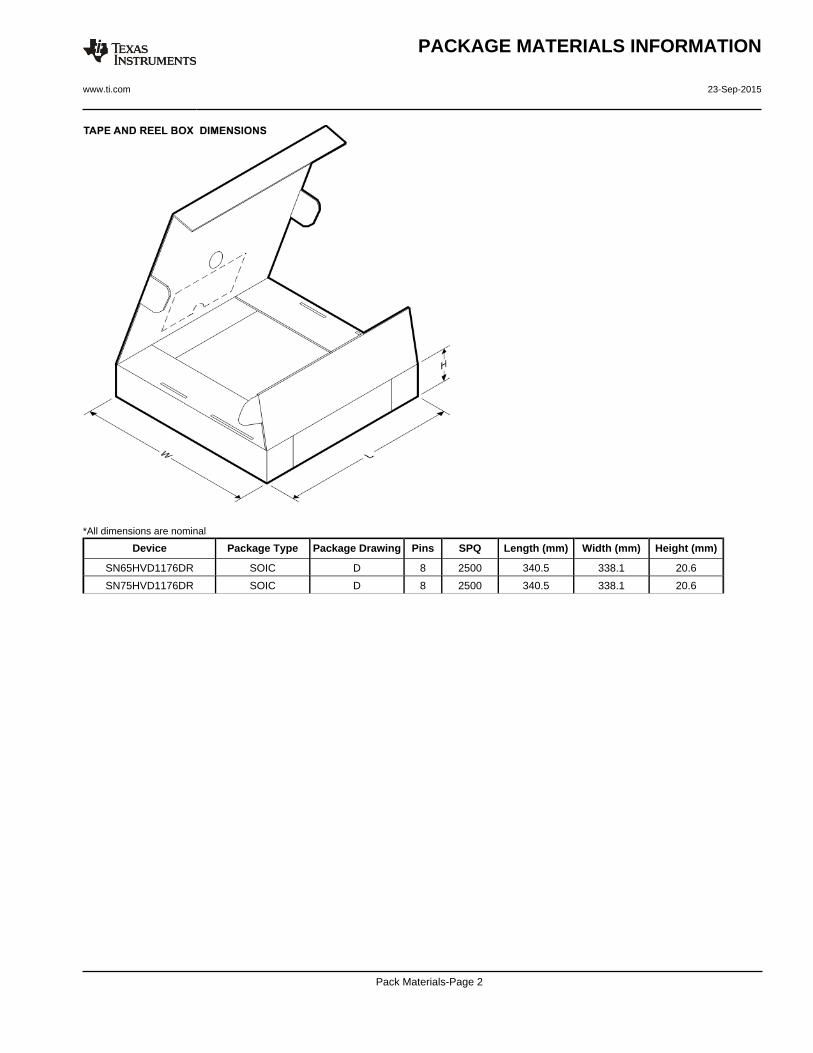
Device Package Type Package Drawing Pins SPQ Length (mm) Width (mm) Height (mm)
SN65HVD1176DR SOIC D 8 2500 340.5 338.1 20.6
SN75HVD1176DR SOIC D 8 2500 340.5 338.1 20.6
PACKAGE MATERIALS INFORMATION
www.ti.com 23-Sep-2015
Pack Materials-Page 2


IMPORTANT NOTICE
Texas Instruments Incorporated (TI) reserves the right to make corrections, enhancements, improvements and other changes to itssemiconductor products and services per JESD46, latest issue, and to discontinue any product or service per JESD48, latest issue. Buyersshould obtain the latest relevant information before placing orders and should verify that such information is current and complete.TI’s published terms of sale for semiconductor products (http://www.ti.com/sc/docs/stdterms.htm) apply to the sale of packaged integratedcircuit products that TI has qualified and released to market. Additional terms may apply to the use or sale of other types of TI products andservices.Reproduction of significant portions of TI information in TI data sheets is permissible only if reproduction is without alteration and isaccompanied by all associated warranties, conditions, limitations, and notices. TI is not responsible or liable for such reproduceddocumentation. Information of third parties may be subject to additional restrictions. Resale of TI products or services with statementsdifferent from or beyond the parameters stated by TI for that product or service voids all express and any implied warranties for theassociated TI product or service and is an unfair and deceptive business practice. TI is not responsible or liable for any such statements.Buyers and others who are developing systems that incorporate TI products (collectively, “Designers”) understand and agree that Designersremain responsible for using their independent analysis, evaluation and judgment in designing their applications and that Designers havefull and exclusive responsibility to assure the safety of Designers' applications and compliance of their applications (and of all TI productsused in or for Designers’ applications) with all applicable regulations, laws and other applicable requirements. Designer represents that, withrespect to their applications, Designer has all the necessary expertise to create and implement safeguards that (1) anticipate dangerousconsequences of failures, (2) monitor failures and their consequences, and (3) lessen the likelihood of failures that might cause harm andtake appropriate actions. Designer agrees that prior to using or distributing any applications that include TI products, Designer willthoroughly test such applications and the functionality of such TI products as used in such applications.TI’s provision of technical, application or other design advice, quality characterization, reliability data or other services or information,including, but not limited to, reference designs and materials relating to evaluation modules, (collectively, “TI Resources”) are intended toassist designers who are developing applications that incorporate TI products; by downloading, accessing or using TI Resources in anyway, Designer (individually or, if Designer is acting on behalf of a company, Designer’s company) agrees to use any particular TI Resourcesolely for this purpose and subject to the terms of this Notice.TI’s provision of TI Resources does not expand or otherwise alter TI’s applicable published warranties or warranty disclaimers for TIproducts, and no additional obligations or liabilities arise from TI providing such TI Resources. TI reserves the right to make corrections,enhancements, improvements and other changes to its TI Resources. TI has not conducted any testing other than that specificallydescribed in the published documentation for a particular TI Resource.Designer is authorized to use, copy and modify any individual TI Resource only in connection with the development of applications thatinclude the TI product(s) identified in such TI Resource. NO OTHER LICENSE, EXPRESS OR IMPLIED, BY ESTOPPEL OR OTHERWISETO ANY OTHER TI INTELLECTUAL PROPERTY RIGHT, AND NO LICENSE TO ANY TECHNOLOGY OR INTELLECTUAL PROPERTYRIGHT OF TI OR ANY THIRD PARTY IS GRANTED HEREIN, including but not limited to any patent right, copyright, mask work right, orother intellectual property right relating to any combination, machine, or process in which TI products or services are used. Informationregarding or referencing third-party products or services does not constitute a license to use such products or services, or a warranty orendorsement thereof. Use of TI Resources may require a license from a third party under the patents or other intellectual property of thethird party, or a license from TI under the patents or other intellectual property of TI.TI RESOURCES ARE PROVIDED “AS IS” AND WITH ALL FAULTS. TI DISCLAIMS ALL OTHER WARRANTIES ORREPRESENTATIONS, EXPRESS OR IMPLIED, REGARDING RESOURCES OR USE THEREOF, INCLUDING BUT NOT LIMITED TOACCURACY OR COMPLETENESS, TITLE, ANY EPIDEMIC FAILURE WARRANTY AND ANY IMPLIED WARRANTIES OFMERCHANTABILITY, FITNESS FOR A PARTICULAR PURPOSE, AND NON-INFRINGEMENT OF ANY THIRD PARTY INTELLECTUALPROPERTY RIGHTS. TI SHALL NOT BE LIABLE FOR AND SHALL NOT DEFEND OR INDEMNIFY DESIGNER AGAINST ANY CLAIM,INCLUDING BUT NOT LIMITED TO ANY INFRINGEMENT CLAIM THAT RELATES TO OR IS BASED ON ANY COMBINATION OFPRODUCTS EVEN IF DESCRIBED IN TI RESOURCES OR OTHERWISE. IN NO EVENT SHALL TI BE LIABLE FOR ANY ACTUAL,DIRECT, SPECIAL, COLLATERAL, INDIRECT, PUNITIVE, INCIDENTAL, CONSEQUENTIAL OR EXEMPLARY DAMAGES INCONNECTION WITH OR ARISING OUT OF TI RESOURCES OR USE THEREOF, AND REGARDLESS OF WHETHER TI HAS BEENADVISED OF THE POSSIBILITY OF SUCH DAMAGES.Unless TI has explicitly designated an individual product as meeting the requirements of a particular industry standard (e.g., ISO/TS 16949and ISO 26262), TI is not responsible for any failure to meet such industry standard requirements.Where TI specifically promotes products as facilitating functional safety or as compliant with industry functional safety standards, suchproducts are intended to help enable customers to design and create their own applications that meet applicable functional safety standardsand requirements. Using products in an application does not by itself establish any safety features in the application. Designers mustensure compliance with safety-related requirements and standards applicable to their applications. Designer may not use any TI products inlife-critical medical equipment unless authorized officers of the parties have executed a special contract specifically governing such use.Life-critical medical equipment is medical equipment where failure of such equipment would cause serious bodily injury or death (e.g., lifesupport, pacemakers, defibrillators, heart pumps, neurostimulators, and implantables). Such equipment includes, without limitation, allmedical devices identified by the U.S. Food and Drug Administration as Class III devices and equivalent classifications outside the U.S.TI may expressly designate certain products as completing a particular qualification (e.g., Q100, Military Grade, or Enhanced Product).Designers agree that it has the necessary expertise to select the product with the appropriate qualification designation for their applicationsand that proper product selection is at Designers’ own risk. Designers are solely responsible for compliance with all legal and regulatoryrequirements in connection with such selection.Designer will fully indemnify TI and its representatives against any damages, costs, losses, and/or liabilities arising out of Designer’s non-compliance with the terms and provisions of this Notice.
Mailing Address: Texas Instruments, Post Office Box 655303, Dallas, Texas 75265Copyright © 2018, Texas Instruments Incorporated