SMART INDUCTION COOKING SYSTEM USING SOLAR ENERGY
85
SCHOOL OF ELECTRICAL, ELECTRONICS AND COMPUTER ENGINEERING SMART INDUCTION COOKING SYSTEM USING SOLAR ENERGY By Bandile Innocent Sibiya 211537771 In Partial Fulfilment of the Master of Science in Engineering, College of Agriculture, Engineering and Science, University of KwaZulu-Natal 01 December, 2017 Durban, Glenwood Dr Chitra Venugopal EXAMINER’S COPY
Transcript of SMART INDUCTION COOKING SYSTEM USING SOLAR ENERGY

SCHOOL OF ELECTRICAL, ELECTRONICS AND COMPUTER
ENGINEERING
SMART INDUCTION COOKING SYSTEM USING SOLAR
ENERGY
By
Bandile Innocent Sibiya
211537771
In Partial Fulfilment of the Master of Science in Engineering, College of Agriculture,
Engineering and Science, University of KwaZulu-Natal
01 December, 2017
Durban, Glenwood
Dr Chitra Venugopal
EXAMINER’S COPY

ii
CERTIFICATE
As the candidate’s Supervisor, I agree to the submission of this thesis.
…………………………………
(Supervisor: Dr. Chitra Venugopal)
DECLARATION 1 – PLAGIARISM
I, Bandile Innocent Sibiya declare that;
1. The research reported in this thesis, except where otherwise indicated is my original research.
2. This thesis has not been submitted for any degree or examination at any other university.
3. This thesis does not contain other persons’ data, pictures, graphs or other information, unless
specifically acknowledged as being sourced from other persons.
4. This thesis does not contain other persons' writing, unless specifically acknowledged as being
sourced from other researchers. Where other written sources have been quoted, then:
Their words have been re-written but the general information attributed to them has been
referenced
Where their exact words have been used, then their writing has been placed in italics and
inside quotation marks, and referenced.
5. This thesis does not contain text, graphics or tables copied and pasted from the Internet, unless
specifically acknowledged, and the source being detailed in the thesis and in the References sections.
Signed:
……………………………………
(Bandile Innocent Sibiya)
iii
DECLARATION 2 – PUBLICATIONS
Publication 1
This research has been presented in the First International Conference on Power Engineering,
Computing and CONtrol, PECCON-2017 and published in Science Direct
Bandile, I. Sibiya and Dr.Chitra Venugopal, “Solar Power Induction Cooking System”,
Energy Procedia, Elsevier, 117(2017), pp.145-156.
Signed:
……………………………………
(Bandile Innocent Sibiya)

iv
ACKNOWLEDGEMENTS
I am greatly indebted to my supervisor Dr Chitra Venugopal for giving me right ways of approaching the
research study, good guidance, encouragement at all time and checking of progress now and then to keep
me up to date.
I am also greatly indebted to Mr Wikus Coetzee from Microcare, for his advises in terms of solar
renewables as he is a specialist and a manufacture.
I would like to thank Mr Renay, Engineering Masters student on campus for helping me on the
programming part of the study.
I would also like to appreciate the support received my mom and the rest of the family by encouraging me
all the way since started my research in 2016.
I would like to thank my friend Nkosingiphile Mbele who was also doing his research in Criminology for
encouraging each other towards completing our thesis this year.
I would to thank specifically my brother Mthobisi Sibiya for keeping me awake while I have to complete
the compile of my thesis.

v
Abstract
Solar energy presents a good, clean and a reliable source of energy for the future. The focus includes the
department of energy strategy (DoE) to allow solar renewables appliances to grow and contribute to the
country’s economy and global environment. This study uses the recent advantage of induction cooking
methods in the market to apply more efficient and economical techniques that go in line with the future
wishes in the energy sector. Induction cooker is proven to transfer at least 80 % of the power generated to
the pot, while electric stove and gas burners generate more to compensate for the power that is transferred
to the atmosphere in the form of heat (i.e. about 55 % efficient). The induction cooker is currently
presenting best cooking technology thus far. Though all including induction cooker are completely
dependent on the grid power. The research comes with the idea of solar energy to fill the big existing gap
of completely depending on non-renewable resources. The advantage comes with the idea of making the
product a completely standalone, reducing electricity bills, simple and reliable, no fuel costs and spills,
flexible in power sources, sustainable development etc. The proposed cooking technology is improved
version and it gives more in the customer needs with regard to clean system, ease to use, conservation and
price. Though initial system installation price is high but after five years, the user will be saving a large
amount of money. The research will improve the annual savings by 45 % as per the DoE analysis in the
comparison of cooking technologies. The thesis focuses on the solar as a primary source of energy to
promote savings. The grid power is still used as a backup power source as we are not yet 100 % green but
gradually adjusting. The design uses the power auto switching method to treat solar power as a primary
source of supply and mains to be the system backup. The cooker battery storage is charged by the solar
using efficient MPPT technology and supply the stove at the same time. The mains only take over when
the solar is completely not available for some time and it will supply the cooker directly via AC to DC
power supply unit and also charges the battery storage via AC to DC battery charger. All the above
switching is programmed and happens automatically via remote programmable relay. System design
includes theoretical background in the form of circuit analysis, power flow and mathematical calculations.
The simulation and practical results present eight different power levels that are displayed in the liquid
crystal display (LCD) in the form of switching frequency and power consumed by the load. The power
mathematical calculations, Simulations and practical results analysis show a similar trend. The pot material
is kept constant while changing switching frequency to achieve desired outputs. Theoretical and
simulations are in line while practical differ slightly due to many factors like component internal
resistances, conductors used and component internal circuit topology. The other adjustments in practical
includes a smaller scale of power (600 watts maximum) compared to simulations due to safety reasons on
my capacity to implement a prototype and proving the working of the study at a smaller scale which can
be extended if required. The general and specific objectives of the study are achieved in simulations and
practical though some adjustments were made during practical in order to me general and specific
objectives. The study proves the theory of energy savings, being standalone product in the practical results
analysis and thus presents many advantages in the commercial sector for the future.

vi
Table of contents
SMART INDUCTION COOKING SYSTEM USING SOLAR ENERGY .................................................................... i
CERTIFICATE .............................................................................................................................................................. ii
DECLARATION 1 – PLAGIARISM ....................................................................................................................... ii
DECLARATION 2 – PUBLICATIONS .................................................................................................................. iii
ACKNOWLEDGEMENTS .......................................................................................................................................... iv
Abstract .......................................................................................................................................................................... v
List of figures .............................................................................................................................................................. viii
List of tables ................................................................................................................................................................. ix
Abbreviations ................................................................................................................................................................. x
1. Introduction .......................................................................................................................................................... 1
1.1 General ....................................................................................................................................................... 1
1.2 Rationale for induction cooking system ..................................................................................................... 1
1.3 Advantages of solar induction cooking system ........................................................................................... 1
1.4 Disadvantages of existing cooking technologies ........................................................................................ 2
1.5 Research objectives .................................................................................................................................... 2
1.5.1 General research objectives .............................................................................................................. 2
1.1.1 Specific research objectives .............................................................................................................. 3
1.6 Methodology .............................................................................................................................................. 3
1.7 Contribution ........................................................................................................................................... 4
1.8 Chapter arrangement .................................................................................................................................. 5
1.9 Funding for the Project ............................................................................................................................... 6
2. Design Methodology ............................................................................................................................................ 7
2.1 Introduction ..................................................................................................................................................... 7
2.2 Literature survey ......................................................................................................................................... 8
2.3 Research methodology ............................................................................................................................. 11
2.4 Design stages ............................................................................................................................................ 12
2.4.1 Stage one ......................................................................................................................................... 12
2.4.2 Stage two ........................................................................................................................................ 12
2.4.3 Stage three ...................................................................................................................................... 12
2.4.4 Stage four ........................................................................................................................................ 13
2.4.5 Stage five ........................................................................................................................................ 13
2.5 Conclusion ................................................................................................................................................ 13
3. Design of solar powered induction cooker ......................................................................................................... 14
3.1 Introduction ................................................................................................................................................... 14
3.1 Design of solar powered induction cooking system ................................................................................. 14
3.1.1 Solar panel and MPPT .................................................................................................................... 15
3.1.2 DC to DC regulator ......................................................................................................................... 16

vii
3.1.3 Mains .............................................................................................................................................. 17
3.1.4 Auto Switching / Relay interface .................................................................................................... 17
3.1.5 AC to DC Converter ....................................................................................................................... 18
3.1.6 Battery storage ................................................................................................................................ 20
3.1.7 Half bridge cooktop ........................................................................................................................ 22
3.1.8 Power flow control circuit............................................................................................................... 26
3.2 Conclusion ................................................................................................................................................ 32
4 Implementation Design ...................................................................................................................................... 33
4.1 Introduction .............................................................................................................................................. 33
4.1.1 Programmable relay, MPPT and AC-DC charger ........................................................................... 34
4.1.2 Battery storage ................................................................................................................................ 34
4.1.3 Induction cooker ............................................................................................................................. 35
4.1.4 Driver circuit ................................................................................................................................... 35
4.1.5 Half bridge ...................................................................................................................................... 36
4.2 Circuit performance .................................................................................................................................. 36
5 System Simulations and Practical results ........................................................................................................... 38
5.1 Introduction .............................................................................................................................................. 38
5.2 Simulation results ..................................................................................................................................... 38
5.3 Experimental results ................................................................................................................................. 45
5.4 Results Analysis and Discussion .............................................................................................................. 52
5.4.1 Simulations vs. Practical ................................................................................................................. 52
5.4.2 Circuit Performance ........................................................................................................................ 52
5.5 Simulation and Practical results comparison and justification .................................................................. 54
5.6 Circuit results analysis .............................................................................................................................. 55
5.6.1 Achievement ................................................................................................................................... 55
5.6.2 Strengths ......................................................................................................................................... 55
5.6.3 Weakness ........................................................................................................................................ 56
5.7 Future work .............................................................................................................................................. 58
6.0 Conclusion..................................................................................................................................................... 57
References ................................................................................................................................................................... 59
Appendix A .................................................................................................................................................................. 62
AC to DC converter calculations ............................................................................................................................ 62
Appendix B .................................................................................................................................................................. 63
Pot resistance vs. switching frequency .................................................................................................................... 63
Appendix C .................................................................................................................................................................. 64
Practical and design cost ......................................................................................................................................... 64
Appendix D .................................................................................................................................................................. 67
Code for the whole circuit operation ....................................................................................................................... 67

viii
Table of figures
Figure 1: System block diagram .................................................................................................................. 4
Figure 2: Design power flow chart ............................................................................................................ 11
Figure 3: Design block diagram ................................................................................................................. 15
Figure 4: DC to DC converter .................................................................................................................... 16
Figure 5: Relay interface internal feature .................................................................................................. 18
Figure 6: AC to DC scheme ....................................................................................................................... 18
Figure 7: AC to DC power supply ............................................................................................................. 19
Figure 8: Cycles life versus depth of charge for several types of lead-acid batteries [26] ......................... 21
Figure 9: Battery charger circuit simulation .............................................................................................. 22
Figure 10: Half bridge inverter model ........................................................................................................ 23
Figure 11: State 1 ....................................................................................................................................... 23
Figure 12: State 2 ....................................................................................................................................... 24
Figure 13: State 3 ....................................................................................................................................... 24
Figure 14: State 4 ....................................................................................................................................... 24
Figure 15: State 5 ....................................................................................................................................... 25
Figure 16: State 6 ....................................................................................................................................... 25
Figure 17: Snubber circuit .......................................................................................................................... 26
Figure 18: Operational range of the half bridge ......................................................................................... 27
Figure 19: Circuit impedance diagram....................................................................................................... 27
Figure 20: Dependence of resistance on switching frequency ................................................................... 28
Figure 21: Output power vs. Frequency ..................................................................................................... 29
Figure 22: Half bridge inverter with the cooker coil .................................................................................. 30
Figure 23: Whole circuit simulation diagram ............................................................................................ 31
Figure 24: Implementation design schematic ............................................................................................ 33
Figure 25: Microcare MPPT charger ......................................................................................................... 34
Figure 26: Battery wiring diagram ............................................................................................................. 34
Figure 27: Cooker diagram ........................................................................................................................ 35
Figure 28: Half bridge inverter .................................................................................................................. 36
Figure 29: Induction cooker, pot, and whole setup .................................................................................... 37
Figure 30: Power level one ........................................................................................................................ 39
Figure 31: Power level two ........................................................................................................................ 40
Figure 32: Power level three ...................................................................................................................... 41
Figure 33: Power level four ....................................................................................................................... 42
Figure 34: Power level five ........................................................................................................................ 42
Figure 35: Power level six ......................................................................................................................... 43
Figure 36: Power level seven ..................................................................................................................... 44
Figure 37: Power level eight ...................................................................................................................... 45
Figure 38: Power level 1 ............................................................................................................................ 46
Figure 39: Power level two ........................................................................................................................ 47
Figure 40: Power level three ...................................................................................................................... 48
Figure 41: Power level four results ............................................................................................................ 49
Figure 42: Power level five ........................................................................................................................ 49
Figure 43: Power level six ......................................................................................................................... 50
Figure 44: Power level seven ..................................................................................................................... 51
Figure 45: Power level eight ...................................................................................................................... 51
Figure 46: Equivalent series resistance for aluminium and cast iron [30] ................................................. 63
Figure 47: Power unit and deep cycle battery ............................................................................................ 64
Figure 48: Whole circuit PCB layout ......................................................................................................... 65
Figure 49: Driver circuit operational diagram ............................................................................................ 66

ix
Table of tables
Table 3 -1 : circuit parameters -------------------------------------------------------------------------------------------------- 29
Table 5 -1: power level one result --------------------------------------------------------------------------------------------- 39
Table 5 -2: power level two results ------------------------------------------------------------------------------------------- 40
Table 5 --3: Power level three results ----------------------------------------------------------------------------------------- 41
Table 5 --4: Power level four results ------------------------------------------------------------------------------------------ 42
Table 5 -5: Power level five results ------------------------------------------------------------------------------------------- 43
Table 5 -6: Power level six results -------------------------------------------------------------------------------------------- 43
Table 5 -7: Power level seven results ----------------------------------------------------------------------------------------- 44
Table 5 -8: Power level eight results ------------------------------------------------------------------------------------------ 45
Table 5 -9: Power level one result --------------------------------------------------------------------------------------------- 46
Table 5 -10: Power level two results------------------------------------------------------------------------------------------ 47
Table 5 -11: Power level three results --------------------------------------------------------------------------------------- 48
Table 5 -12: Power level four results ----------------------------------------------------------------------------------------- 49
Table 5 -13: Power level five results ----------------------------------------------------------------------------------------- 50
Table 5 -14: Power level six results ------------------------------------------------------------------------------------------- 50
Table 5 -15: Power level seven results --------------------------------------------------------------------------------------- 51
Table 5 -16: Power level eight results ---------------------------------------------------------------------------------------- 52
Table 5 -17: Simulations and Practical overview ------------------------------------------------------------------------- 52

x
Abbreviations
DoE Department of Energy
AC Alternating Current
DC Direct Current
LCD Liquid Crystal Display
MPPT Maximum Power Point Tracking
CO2 Carbon Dioxide
PWM Pulse Width Modulation
V Volts
A Amperes
AH Amperes-Hour
IGBT Insulated Gate Bipolar Transistor
PV Photovoltaic
W Watts
Vs. Voltage Source
Cr. Resonant Capacitor
ZVS Zero Voltage Switching
SW Square Wave
Rs. Rupee
FEM Finite Element Model
CB Circuit Breaker
VL load Voltage
RCL Resistor-Inductor-Capacitor
ZCS Zero Current Switching
KHz Kilohertz
RMS Root Mean Square

CHAPTER I
1
1 Introduction
1.1 General
Solar energy is a good and clean source of energy, which can help the world in experiencing the dirty and short
of non-renewable resources, such as coal, etc. The country has accepted that the emission of greenhouse gases has
led to increasing concerns about climate change. The department of energy (DoE) has developed a strategy in
which the renewable energy sector can operate to grow and contribute positively to the country’s economy
together with global environment [7]. Induction cooking has been implemented long ago but lacking some
advancement. The induction cookers in the market use mains power to operate of which limits the flexibility in
terms of power sources. The working principle of the project is similar to what is in the literature, but with more
of advancement features using auto selection in terms power sources, i.e. solar and mains AC power with the
addition of battery storage as a backup and also to make it a complete portable standalone product. The benefits
include economical, pollution free and sustainable energy conversion process as solar energy is adopted as the
source.
1.2 Rationale for induction cooking system
The induction cooking system technology is one of the best cooking methods that have been developed up to date.
The trending advantage includes high efficiency that is almost two times the existing technologies. The efficiency
comes with low power consumption i.e. all power that is generated is transferred at least 80 % of the generated.
The existing technology, electric stove and gas burners generate large amount of power in order to compensate
for the power that is transferred to the surroundings in the form of heat. If taking a look at the research, as above
induction cooking stove is the best cooking technology thus far. All of the above including induction stove is
completely dependent into electricity generated by Eskom. The introduction of solar energy comes with the aim
of filling the big gap existing amongst the use of electricity that is 100 % dependent on non-renewable resources.
Below is the list of advantages and disadvantages of solar powered induction cooking system compared to the
electric stoves.
1.3 Advantages of solar induction cooking system
Reduce electricity bills
Completely a standalone product
The high harmonic semi-sine wave generated during induction process
Easy to install
Simple and reliable

CHAPTER I
2
Safety
Low maintenance
No fuel cost and spills
System can be made to be mobile
High radiation index
Auto power selection method (flexible in power sources)
Sustainable development
1.4 Disadvantages of existing cooking technologies
Dependent on non-renewable resources
The cost of electricity bills and gas increases with resource demands
Large amount CO2 emission
Electric stove is slower to cool down
Electric stove may not work during storms (due to power outages)
Gas is dangerous due to possibility of gas leaking
Gas give off humid heat rather than dry required for effective roasting
The above advantages and disadvantages regarding existing cooking system compared with the proposed cooking
technology create an improvement in cooking systems and it gives more options to the customer needs with regard
to safety, ease to use, cleaning systems, conservation, and price.
1.5 Research objectives
1.5.1 General research objectives
The general objective of this research is to simulate and build a solar powered induction cooking system using
auto selection method for any available power source, taking solar panel power as a priority for encouraging
savings from using the grid power. Solar powered induction cooking system should be designed as a complete
standalone product that is also portable and it can be used everywhere with the advantage of battery storage that
is charged either by the panel or the mains itself if it happens the sun is not available for days. The aim also covers
the reducing of electricity bills as the electric stove uses more power while half it is wasted as heat energy in the
kitchen.

CHAPTER I
3
1.5.2 Specific research objectives
Design and simulate an induction cooking system with eight programmed power levels.
The design needs to accommodate calculations of the input power levels; half bridge, induction coil
calculations, resonance frequency value, and pot resistance range of values and plot it in a graph for best
pot material selection.
Write a code to accommodate eight power levels and test it on the program script.
Run the code on Proteus software and check for errors.
Show each power level on the graph by means of PWM, load current and load voltage line graphs on
oscilloscope.
Design and simulate a charging circuit, AC to DC converter and charging circuit.
Design and simulate LCD display for different power level and respective switching frequency.
Build a DC to DC regulating system (MPPT) that is interconnected with the solar panels to monitor
charging of the battery storage at 48 V and a maximum of 20 A charging current.
Build an AC to DC converter that is fed from 230 V AC mains supply socket with an output voltage of
48 V, 10 A maximum to charge the battery and also be able to supply the half-bridge inverter circuit.
Design and build a smart auto selection switch and connect it with the solar system and AC to DC supply.
Build a charging control circuit for both solar and grid power.
Build a half bridge inverter circuit with two N-channel IGBTs and design a induction coil and connect
it in the middle of the IGBTs to form an induction cooker half bridge inverter.
Build and program a power control circuit with eight different power levels corresponding with its
switching frequencies.
Test the Programmed LCD to display power levels as per the user selection.
Integrate the whole system and demonstrate each and every power level with respect to the user selection.
Test the auto selection switch, test if charging is working for solar and mains.
Test the standalone feature for the cooker.
Show graph of PWM, load current and load voltage and compare practical and simulation graphs.
Overall design analysis, drawbacks, and future improvement suggestions for the continuation of the
research.
1.6 Methodology
The design system is connected into two power sources, i.e. mains and solar (with battery storage assist system).
The first supply of which is mains power is connected to an AC to DC converter (battery charger) of which is then
interconnected with charging control circuit. The second supply solar panel is first connected with the DC to DC
regulator, and then goes to the charging control circuit as well. The charging control circuit is than connected to
the auto-switch circuit that directly feeds the half bridge inverter (induction cooking system). The induction

CHAPTER I
4
cooking system is having input buttons for control purposes and according to the user need. The output of the
cooker is having eight different power levels with different switching frequency.
Figure 1: System block diagram
The above block diagram in fig. 1 shows all the stages of the design from two power sources (solar and mains) to
the induction coil. The solar is taken as a priority in the power source selection as this is part of it advantage to
promote free use of available energy from the sun. The design of each block is done using theoretical calculations
and simulated in Proteus and Multism software packages. The theoretical, simulated results are compared with
practical results obtained from the built system.
1.7 Contribution
Currently the country has developed the strategies by introducing a long term goal for renewable energy
sustainability development in 2003 and wish to accomplish 42 % renewable based capacity by 2030 [7]. The use
of renewable resources especially solar is always on the engineering articles nowadays. The funding for the
renewable based research is all over the country as to meet the 2030 target.
All the research papers discussed in the literature in chapter two discusses about different methods to do induction
cookers, the material of the coil, the distance between the coil and the pot and how the efficiency can be improved.
All the cookers are power dependent to Eskom / mains power to operate and the cookers still utilise fossil fuels
100 % of which oppose what the country is looking to achieve. The power levels are few compared to the eight
that are produced in this study. The focus on the previous study is more on being creative but not answering the
country in terms of meeting the future goals / demands. The current method used in this study is similar to the
existing study but putting improvement and also addressing the country problems by making it mains and
renewable based. Mains power is still considered in the design since the country still consist of more fossil fuel
based utilities. The research also contributes in the financial relief for high electricity bills from the home stoves.
The research focuses in the theory, simulation and prototype building and testing of the induction cooking system.
CHAPTER I
5
The research is also more about making the cooker a standalone, completely independent from nonrenewable
resources and smart in operation by being more user friendly and introducing more cooking levels to suit user
needs. Smart cooking is introduced to improve the cooking in a more efficient and easy way by allowing the
cooker to use solar energy as the primary source of energy and also be able to use mains as the alternative power
source option. The cooker uses the auto selection of any available power source by doing the load power analysis
and also in accounting for the savings (solar energy).
1.8 Chapter arrangement
The research content is organized in six chapters,
Chapter one: this chapter discusses about the history of the research on how it was done and how this present
research is going to fill in the existing gap. This is explained by general and specific objectives of the research
stated above. The chapter continues to show and explain the design methodology step by step to achieve general
and specific objective of the research. This chapter also focuses on the contributions of this research on the existing
research and how it will add a commercial value to the research.
Chapter two: in this chapter, induction cooking methods are discussed by explaining the major objectives and
findings in each literature study presented and how it is related into this research by find the gaps in terms of the
methodology used in the papers. The chapter also states how the gaps will be resolved in terms methodology,
accuracy in findings and commercial value of the final product. The block diagram is explained in details by
addressing the general and specific objectives of the research.
Chapter three: the design of the solar powered induction cooking system is presented in details by means of
theoretical calculations and software simulations. The practical overall diagram is shown and explained in details
by means of any adjustments made during the implementation section.
Chapter four: in this chapter, all the simulation and practical results are shown for each and every block in the
block diagram that was presented in chapter three. The deviations or adjustments are explained in details.
Chapter five: The chapter focusses on the analysis of results and discussions. The results are analysed to explain
if the general and specific objectives are achieved or not. The advantages and disadvantages of the design are
discussed accordingly. The future of the research is discussed by means of suggested methods to improve the
results.
Chapter six: this is the last chapter of the thesis. The purpose of the solar powered induction cooking system
compared to the traditional existing cooking methods. Explain how the final results have overcome the shortfall
of the literature explained chapter two. The methods used to achieve the general and specific objectives are
discussed in brief. The quality and standard of the research is explained and together with the commercialisation
of the product. The improvements are explained for future research opportunities.

CHAPTER I
6
1.9 Funding for the Project
This project has been funded by CSIR, UKZN from 2015-2017. The funding was granted to carry a renewable
based project Solar powered induction cooking system. The funding has been granted for two consecutive years
to further continue and complete the study.
CHAPTER II
7
2 Methodology
2.1 Introduction
Oil and gas are most commonly used fuels for power generation. Prices of such fuels are rocketing and the use of
such fuels severely affects the environment. Global warming and green house effects are the main threat for the
natural living system at the present situation and for the future generations [8]. Usage of fossil fuels for power
generation is also one of the main causes for the environmental pollution. Sources which are environmentally
clean, low in cost and easily accessible can serve the global community in a better way to save the environment.
Solar power generation received significant attention due to many advantages such as less maintenance, no wear
and tear and absolutely no cost for fuel apart from the factors discussed above. PV modules are used to generate
electricity from sun [8]. Due to the non-linear characteristics of PV system, the output power is not constant all
the times through the day. For the research, maximum power point tracking regulator is used to regulate the
unregulated PV system.
Induction heating in nowadays is widely present in domestic appliances because of its cleanliness, high efficiency,
safety and performance [2]. Induction heating is the process of heating an electrically conductive material (usually
a metal) by electromagnetic Induction [2]. The time varying magnetic field around the conductor coil induces
voltage and causes hysteresis losses as a form of heat when is exposed to a ferromagnetic material (pot) [4].
Induction heating allows high speed of heating and dissipation, all the heat produced is approximately transferred
to the pot (greater than 80 % in efficiency) [1].
As presented above, solar and induction cooker provide cleanness and present high savings factor with regard to
the use of massive free energy and high in efficiency by delivering more than 80 % of power output respectively.
The high harmonics current generated from DC to AC conversion gives an advantage to the induction coil during
coupling to give more current to the load and thus generate large amount power.

CHAPTER II
8
2.2 Literature survey
The analytical electromagnetic of domestic induction heating system is presented in [9]. The paper discusses about
engineering principle of magnetic coupling between the system and the effect of it in the system operation together
with looking at the mathematical calculations of the circulating currents and the contribution of it in the system
load together with its amplitude to give rise to heating efficiency. The method and the approach used in the paper
is similar lies within what is presented in all the literatures about induction cooking system. The paper touches
important aspects, pot (load), coil and how the coupling affects the efficiency of the output power. The analysis
is looking at the voltage and impedance matrixes and how these can give values of current and impedance in order
to analyse induction system operation. The number of tests is performed in an experiment. The contribution comes
with fact of getting to know how electric and magnetic currents describe the equation of potential balance of the
system and how electric field and magnetic field can used to get self and mutual coefficients. The paper leaves a
big gap in how the switching frequency is controlled, what method of switching is use either zero current switching
or zero voltage switching, how the study can contribute to the community, only relies on one power source, no
simulation study presented, et c. The study need to improve by addressing all above in order to promote research
that will show how the study can be taken into practise to help our communities in the problems they facing.
Taking note of the existing gap in the paper, induction cooking is now in the market and it efficiency, cleanness
and safety is putting it as a number one stove compared to the ones existed long ago. Now the focus is to how the
induction cooker in the market can be utilised in a more sustainable way by addressing the issues facing the
country in taking renewable energy into practise as a DoE sustainability development. The study will design and
build a portable solar powered induction cooking system that uses auto-switching method to make it flexible in
terms of power sources by allowing it to be used either by solar or mains and it also present a battery storage that
can be charged by both the power supplies, of which makes it a complete standalone which can be run without
both power sources being available.
The design of zero voltage switching (ZVS) series resonant inverter is presented [10]. This paper touches very
important sections for induction cooking system, i.e. influence of load, snubber circuit and dead time. The paper
firstly discusses about ZVS of which is the method used in my study and it most in all the literatures, the method
is very efficient and it increase the performance, it also cheap to construct. This study is also focuses in the
efficiency of the induction cooker by looking at the existing traditional square wave (SW) modulation that operate
in high frequencies to give low medium power levels. The proposed solution of this paper is to use a variable
frequency duty cycle control to improve efficiency in the low and medium power levels by decreasing the
switching frequencies. The gap still exists since it only focusses in the efficiency and in the parameters of the
cooker to make it cheap and the best in the power output. This study does not answer the problem the country in
trying to address in terms of how electricity that has been produced by non-renewable resources can be replaced
in the future or either how it can be supplemented by the renewables as part of the sustainable development by
DoE.
The solar-based induction cook top is discussed in [11]. This paper discusses about the solar powered induction
cooking system. Each stage from solar panel, control circuit, battery, inverter and cook top is presented in details.
The microcontroller and the LCD (liquid crystal display) for cooking level indications and control. The aim of the

CHAPTER II
9
paper together with its conclusion was to implement a solar-based system with the idea of looking at the feasibility
and advantage of using solar rather than electric or gas supply. The study proved that the installation can be costly
but after 5 years, the user will be saving a large amount of Rs 12000. The study is in line with the goal of the
sustainable development but lacking some advancement. The study did not consider the fact that the most of the
country is currently running of Eskom electricity with the lack of renewable based capacity of which means it was
going to be perfect if it considered the auto switching between the mains and the solar and introduce more power
levels as to meet the user needs for different cooking stages. The idea of the paper was to compare the price
savings that comes with the induction cooker compared to the gas and electric stoves. The study can be more
improved if it can look at the real problem that is facing the country in terms electricity point of view.
The analysis of an induction-heating device with half bridge resonant inverter is presented in [12]. The circuit
analysis and simulations of the inverter shows the eight function models of the circuit structure. The phenomenon
of the skin effect plays a role in the analysis of the circuit. The study also look at the two factors that resulted in
the temperature of the coil i.e. loss during current flow in the coil and the heat produced by the pot during
operation. The paper focuses on the circuit analysis by looking into detail how the current flows in the circuit and
how the same output current can be achieved using different material of heating coils of which is more of
experimenting the theory learn in class rather using the theory into real life application by addressing major issues
in the country into real problem solving. The study does not look into how the study can be utilised to solve the
current cooking technology to it best. The paper is having great information that assisted the current study that I
am doing. The information for circuit analysis and how many factors affect the operation of the inverter topology.
The study can be improved by taking the theory and simulations that were performed into practise by looking at
the existing gaps in research environment to address real life issues faced by the country.
The induction cooking assessment paper discusses about the comparison between the induction cookers, electric
heating element stove and finally the gas burners [13]. The cooking efficiency ranges from 80 to about more than
90 % for the induction hob and about 50 to 74 % in electric stoves and lastly about 40 % in gas burners. The DoE
after all the tests saw that induction cooking technology reduces the energy saving about 45 % compared to
conventional electric stove [13]. This paper gives this thesis a go ahead and encouragement that the proposed
solution of which addresses the efficiency improvement as discussed compared to the other cooking technologies,
secondly addresses the issue of renewable based appliances as the country is aiming for the 42 % renewable based
capacity by 2030.
Customer’s satisfaction and attitude view amongst the induction cooking was done in city of Tirunelveli [14]. The
study looks at the number of different induction cooking stoves since every company is marketing their cooktops
with more performance and features. The preference and attitude is being investigated towards induction stove.
The paper presents the advantages and disadvantages of advantages overcome the bad view of it. The level of
satisfaction is about 80 % compared to the ones being dissatisfied. The relevance of the study with the current
study comes with the fact that people are willing to invest in the induction cooking environment of which promotes
the study in terms understanding the customer’s attitude and satisfaction amongst the induction cooking
technology that is presented in this research. The research takes this advantage and adds more features that will
be in line with the country’s goal for the sustainable development in the renewable energy sector. The journal

CHAPTER II
10
does not focus in the power sources or in how the cooker is being powered but only look at the features like
efficiency, safety, savings and etc.
The phenomenon of eddy current is widely understood since it explored in all the literatures [15]. Induction
heating is highly used in industrial applications. There is also huge amount of work form academia and industry.
This field is matured with a large number of innovative designs presented each year from academia [16, 17]. The
FEM simulation model of conventional induction cooker is discussed in [18].This model focuses more on the two
parts; namely wok and the coil. The modelled coil shows the even distribution of current in it. The overall
simulation study conclude that magnetic field of the conventional cooker is uneven and localized which can lead
to hot spot in the coil during operation and result in poor performance. The new method of changing the variable
turn coil pitch by allowing the magnetic field to cover wide area improves the heating performance of the induction
cooker. The overall aim of the paper was to emphasize and prove the importance of the variable turn pitch coil in
the heating performance of the induction cooker and to investigate the structure together with problems associated
with heating performance regarding conventional induction cooker in the point of magnetic field distribution. The
effect of the pan material in an induction cooker and the topologies for an induction converter circuit is discussed
in [19]. The comparison of the boost converter (quasi resonant) and resonant converter (half bridge) is studied.
Five pans were tested. The frequency increases with the decrease in current and power proportionally. It concludes
that pushing switching frequencies higher will reduce the cost of the coil, resonant capacitor, and increase the
efficiency of the cooker. The induction cooker as a working electric transformer that generate heat on the
secondary due to loading of the equivalent resistant of the losses is discussed in [20] The paper discusses in detail
all the parameters from the coil to how the current density differs with respect to the number of turns in the coil.
The modes of switching “hard switching” are studied in details showing how the power electronic device behaves
under stressful switching. It also looks at the losses when the switch is exposed to high voltage and current at the
same time. Snubber circuits assist in voltage transients on the switch during switching. The paper also focusses
on the different topologies discussing the parameters in details. The simulations also support the theory in
explanation. The control algorithm for both the topologies is discussed of which shows a slight difference between
the two. The pan detection and circuit protection is presented in details in the flow chart. The practical discussion
of the results corresponds with the simulations.
Currently the problem of trying to move away from non-renewable to more renewable based capacity still leaves
a big gap in research as to how the country’s mandate for sustainable development in renewables be achieved.
This study is part of the government strategies to increase the renewable energy capacity and also the renewable
based appliances. The research will improve the annual saving by 45 % as per the DoE analysis in the comparison
of cooking devices list in the Table 3 of paper [13].
In summary, most the papers discusses about the principle of induction cooking using mains as a supply and only
few that discusses about the working of the cooker using renewable energy as a source of energy. The cookers on
market on the research as the above focuses more on the pan material and on how it affect the performance in
terms of heating the coil and producing more electric field. It also covers more deeply in the switching frequencies
and on how changing the frequency can be done using power electronic switches. The protection also plays a vital
role since the generated magnetic field can cause such high currents in the plate. Topologies are discussed in all
the literatures and all the conference papers. The topology selection is very important as they all play different

CHAPTER II
11
roles with respect to efficiency and cost effectiveness. The study on this research is a solar powered induction
cooking system that works in a similar manner using the principle of magnetic fields induction to cause eddy
current to flow in a ferromagnetic material resulting in heating. The study focuses also on the auto switching
method for selection between two-power source, namely solar power and mains AC power. The auto selection is
to select any available source of power between the two. The cooker uses the batteries that is to be charged by
both solar and mains but treating the solar as a priority always in order to promote the use of free energy when it
available. The cooker also work with batteries alone of which makes it completely portable and being a standalone
product that can work for about 4 hours without solar and the grid being present at the time. In this research, the
simulation study is done for testing the heating level at different frequencies. The practical implementation using
solar and mains switching is also shown in the implementation section.
2.3 Research methodology
The flow chart diagram in the Fig. 2 below shows the power flow of the system in detail. The chart shows how
the interface responds to the user selection. The system consists of an LCD display to indicate power level and
switching frequency and also gives the system status for any user input. The program in the flow chart first asks
the user to select desired power level. The selected power will send a specific signal to the system and the system
will do a power analysis to check if the battery power is enough to supply the system. If the battery is not enough,
the system will automatically switched into mains supply. After the cooking is done, the mains will than charge
the battery.
Figure 2: Design power flow chart
The design consists of two power sources, i.e. solar and mains power. The two power sources are connected
directly to the system. The mains power provides with +/- 230 V and that is converted into direct current via the

CHAPTER II
12
converter since the system requires direct current input. The converted DC voltage is 48 V that is able to charger
the battery storage and also be able to independently supply the system. The converter is connected with the first
section of the battery charger control circuit for mains supply charging. The second section of the charging circuit
is the MPPT regulator that is connected to the solar panel, if solar is selected to charge the battery instead of
mains. This means that the battery storage can be charged either by solar or mains power but treating solar a
priority power source. The MPPT is design to regulate the unregulated/ fluctuating DC voltage from the panel.
Two panels of each 300 watts are used to provide a maximum of 600 watts. The user interface with the buttons is
designed for the user to be able to select any power level required. Each power level is programmed with a specific
switching frequency. The switching frequency is controlled by means of the duty ratio. Each complete circle of
the pulse width modulation (PWM) is accommodated with a switching dead time of +/-5 % to allow the switches
not to switch at the same time as this might result in a short circuit. The switching method used is zero voltage
switching (ZVS), i.e. no voltage will be across the switches during the switching. The ZVS is achieved by
switching at frequencies higher than the resonance frequency.
2.4 Design stages
2.4.1 Stage one
The first step is looking at the theoretically study by drawing each circuit for a specific block in the block diagram
shown in chapter one. After the circuit analysis is done, the theory is translated into mathematical calculations for
each component to be used in the design.
2.4.2 Stage two
The theory and calculations is now taken into software for simulation analysis. The simulation study is to indicate
if the proposed circuits together with it calculations can be simulated and compared with what is in the theory.
The graphs are shown and the values are tabulated accordingly.
2.4.3 Stage three
The simulation study is now taken into practise. The feasibility of each circuit in the block diagram is designed
and tested if it corresponds with what is in the theory and calculations.

CHAPTER II
13
2.4.4 Stage four
After each circuit in the block diagram is achieved in the form of implementation, the integration of the whole
circuit is tested and the results are recorded. All the recorded results are compared with what is in the literature
and what is in the general and specific objectives of the research.
2.4.5 Stage five
This stage presents the overall results analysis and discussion, providing detailed explanation how the completed
product will address all the issues mentioned in the literature by looking at the financial point of view, savings
and its efficiency. The standalone feature is tested in this stage.
2.5 Conclusion
To conclude, the country is investing a lot in renewable based research in aiming to address the current issues
with regards to electricity price, demand, and toxic gases released by non-renewable resources. The literature
presents the existing research that is addressing many areas regarding induction cooking technology. This specific
research is aiming using the literature to address the issue of relying more in non-renewables and trying to help
the country to achieve its on-going of renewable sustainable development. At this stage of the thesis, the
confidence is 80 % that the design will successfully address all the mentioned missing improvements in the
existing literature.

CHAPTER III
14
3 Design of solar powered induction cooker
3.1 Introduction
Solar powered induction stove is about to improve the annual cooking energy costs about 45 % as discussed in
the literature chapter II. The solar induction cooker presents cleanness, high savings with regard the free energy
from the sun and lastly by delivering more than 80 % efficiency in terms of the power output. All the facts has
been gathered from first and second chapter on the research about how solar can be of good and reliable source
of supply for domestic applications as the country is facing utility power issues with regard to the load shedding
Problems as a result of planned and unplanned load-shedding that cause inconvenience. The cooker as reliable
product present features like, battery storage as a backup that makes it a completely standalone product in the case
solar is not available at the time. The theory of the design has been explained in detailed from the first two chapters
including the general and specific objectives of the research. This chapter combines all the general and specific
design objectives into reality in terms of performing relevant calculations and simulation models for each block
in the block diagram explained in chapter one. A pulse width modulation technique is used to control the cooking
power levels as per the user input. The below section concentrate more on the mathematical and schematic design
of the design.
3.1 Design of solar powered induction cooking system
The block diagram below in Fig. 3 shows the overview of the design stages by indicating the important blocks
that plays a vital role in the circuit operation. The power flow is indicated by the arrows, showing how the
communication between the blocks is conducted respectively. The design consists of two power sources, i.e. solar
and mains power. The solar panel is having PV solar cells that convert light energy into electrical energy by means
of direct current. The converted DC value depends on the amount of light intensity as to how much it can extract
from the maximum power a panel can produce. The two panels of each 300 watts are combined to make 600 watts
maximum. The panel voltage and current are having non-linear behaviour since their output is unregulated. The
solar assist function (MPPT) is initiated to assist the power control from the panel to the battery for charging. The
MPPT function will buck and boost the voltage and current to meet charging demand of the battery unit. The
battery unit is 48 V and 25 Amps in capacity. The MPPT makes sure that the battery is charged and discharged
accordingly, as to lengthen the life of the battery unit. The regulator unit has fast charging capabilities to make
sure that battery is charged at it fastest rate. The regulator is than connected to the relay interface. The relay
interface communicate with both the power sources by making sure the power flow is from the correct source at
a specific time. It also makes sure that there is no reverse power flow and that solar is the main power source for
the cooker while the mains are a backup source. The relay is the mind of the system and every decision it takes is
initiated by the circuit breakers. The relay contacts are connected such that if the solar power is immediately
disconnected or there is no enough energy to supply the battery unit, the relay checks if the battery power is still

CHAPTER III
15
enough to provide power to the cooker. Thereafter the relay will make a decision as to close the relevant circuit
breaker to check and allow the mains to take over in powering the cooker. At the same stage, the relay will close
another breaker to make sure that the battery is also charged by the mains for it to remain full. The second power
source is of which is mains is connected to AC to DC converter to produce the same voltage for charging and for
supplying the cooker directly. The converted DC from the mains will sufficiently supply both the battery and the
cooker at the same time. The half –bridge cooktop is the main receiving end of the design. The cooker only seat
and wait for the user input, thereafter it sends a message to the relay asking for the power availability. The relay
will then do the above mentioned steps to check for the best suitable power source depending on the availability
and user power level demand.
3.1.1 Solar panel and MPPT
The PV system converts the solar radiations falling on the PV panel into electrical energy. The converted energy
is directly proportional to the amount of sun’s radiations received by the panel at a specific time of the day. Two
solar panels are connected to give a maximum of 600 watts of each contribute 300 watts maximum. The system
is designed to charge a 48 V battery 25 Ah in capacity. The solar is the primary source of supply for the cooker.
Solar is made up of photovoltaic cells that converter solar energy into electrical energy in the form of direct current
[21]. PV modules generate electricity from sun [20]. Due to the non-linear characteristics of PV systems, the
output power is not constant all the times throughout the day. In this design, batteries, maximum power point
tracking function work together with PV systems to regulate the voltage of the PV systems. In this research, solar
is the main source power for heating the induction coil and 300 W solar panels are used. This unit depends on the
sun radiation to supply energy but using battery storage for stability. Below are the theoretical calculations for the
Figure 3: Design block diagram

CHAPTER III
16
design of solar panel system. Firstly battery capacity is 48 V and 25 Amp Hours (AH). The conversion of AH into
watts is required and the conversion can be seen below;
𝑃𝑎𝑣𝑎𝑖𝑙𝑎𝑏𝑙𝑒 = 𝐴𝐻 𝑥 𝑉𝑏𝑎𝑡𝑡𝑒𝑟𝑦 (1)
AH = Battery size
Vbattery = Battery Voltage
Pavailavle = available power in watts hour (WH)
𝑃𝑎𝑣𝑎𝑖𝑙𝑎𝑏𝑙𝑒 = 25𝐴𝐻 𝑥 48𝑉 = 1200 𝑊𝐻
The equation above shows that 1200 W of power can be supplied for 1 hour, and 600 W in 2 hours etc. The energy
intake is proportional to battery discharge. The amount of power in a battery (battery size) can be always adjusted,
48 V, 25 AH battery is used for research purposes only. Though the rule of thumb says battery can give as much
as 50 % of its capacity as there is a drop in voltage as power is dissipating. The amount of power the panel can
give to the battery is calculated as 2 x 300 W panels multiply by the average hours of the sun during the day. South
Africa receives huge amount solar radiation ranges between 16.2 MJ / m2 to 23.4 MJ / m2 per day [22]. The
average amount of sun in Kwa-Zulu Natal is 6.5 hours and the charging amount can be calculated as 600 W
multiply by 6.5 hours to give 3900 W. This means that the system can charge the battery to its full state three times
in one day.
3.1.2 DC to DC regulator
Fig. 4 shows the simulation diagram of the implemented scheme. In the proposed simulation study, both MPPT
and output DC voltage regulation are carried out. Regulation is needed to provide constant voltage at all times as
solar output fluctuate all the time.
Figure 4: DC to DC converter

CHAPTER III
17
The converter regulates the unregulated DC supply of the solar panel. The smooth DC supply is necessary for the
charging unit to be regulated DC for charging purposes and to supply the inverter with smooth supply. 75 V DC
to 48 V DC converters is used in the simulation. The solar voltage is 37.5 + 37.5 V DC and at 8 A maximum. The
regulator will then convert the 75 volts from the series connected panels to 48 volts to match the system
requirements.
3.1.3 Mains
The mains power is directly connected to the grid. The need for the mains power is to provide backup system for
the design and to make the product more user friendly in terms its flexibility regard power sources. The grid is
directly connected to the system via the AC to DC converter. The grid provides +/- 230 V AC and that is converted
to 48 V DC to meet the system voltage specification. The converter is charging the battery storage at 48 V DC.
The mains play a role only if the solar cannot provide enough charging for the battery storage. The grid will charge
the battery using the converter and also it can directly supply the cooker during the times of no solar available for
a long period. The smart programmable relay is used to do the automatic switching in the above given cases.
3.1.4 Auto Switching / Relay interface
The auto select switch makes the auto selection of any available supply between solar and the grid and select
whichever is sufficient by doing power demand analysis. The solar power is priority in the analysis for cheap
selection and usage. In simulation, the auto switch is controlled by microcontroller program. The battery power
level is compared to the switching state selected. If the battery level is sufficient the coil is powered from the
battery. In this design, the auto switch is programed such that the source selection is done at the beginning of each
cooking state. If the battery is not sufficient to supply the required power for the cooking state selected and for
the duration calculated, the mains power will be selected and the battery will be charged either from solar or from
mains. In this section smart programmable remote relay will be used in the practical section to make things easier
for the implementation due to time frame. The relay switch act as the load shed controller, day night switch and a
solar assist function.

CHAPTER III
18
Figure 5: Relay interface internal feature
The flow chart in Fig. 5 above only show the specific actions for it purpose in the auto selection. The relay is
programmed such that from the beginning it asks if the solar power / battery are available. If the solar / battery is
available and enough to supply the load, the circuit breaker (CB) is closed such that power flow from solar system
to the load. In the case that the solar systems have no power, the second step is to check for the backup power
(mains). If the mains power is available, it respective CB will be closed by the relay signal allowing power flow
from the mains to the load. If the both power is not available, the relay will keep on checking for the power
availability by following the same flow as explained and indicated in the diagram above.
3.1.5 AC to DC Converter
AC power is commercially inexpensive and easily available while DC power is expensive to generate. However,
rectifiers are used to convert the readily available AC power to DC [23]. Rectifiers produce DC voltage with very
high ripples and filters are required to smooth the DC to around a constant value [24]. The filters are divided in
inductor, capacitor and capacitor – inductor filter. The filter selection depends in the application. The capacitor
filter is for low, inductor for high power applications [25]. The mathematical expressions for capacitor and
inductive filters do exist [25]. The DC is having three types of rectifiers namely, half-wave rectifier, full-wave
rectifier and full-wave rectifying bridge. The Fig. 6 below shows the AC to DC scheme.
Figure 6: AC to DC scheme

CHAPTER III
19
Considering the AC input voltage as sinusoidal. The full-wave rectifying bridge is selected as it more
advantageous compared to the other ones. The load voltage and current are defined by the equations below;
𝑉𝑑𝑐 = 2.𝑉𝑠
𝜋 (2)
𝑉𝐿 = 𝑉𝑠
√2 (3)
𝐼𝑑𝑐 = 2.𝑉𝑠
𝜋.𝑅𝐿 (4)
𝐼𝐿 = 𝑉𝑠
√2.𝑅𝐿 (5)
The mains source voltage is taken as 220 volts from the AC socket for calculations and simulations (see appendix
A). Equation 2 is the expected DC voltage at the output, eq.3 is the load voltage and eq.4 and 5 is the DC and load
current equations respectively.
The mains power is an alternating current while the system requires direct current supply. AC to DC conversion
is necessary for the design as above. The converter will be able to charge the 48 V batteries and also supply the
load direct in case the solar power fails. This part of the thesis is not designed from first principle but the converter
will be ordered using the solar panel specification in section 3.1 above. The charger will charger as fast as the
solar panels.
Figure 7: AC to DC power supply
CHAPTER III
20
The above Fig. 7 is the simulation schematic of the AC to DC power supply. This converter makes it convenient
for the batteries and the half bridge converter to work perfectly since the implementation needs only DC supply.
220 V AC is converted to 48 V DC at 542 W power level. The other most important factor is to make it flexible
in the range of frequencies for different power levels in the inverter section.
3.1.6 Battery storage
Energy storage in history has reflected as the most complex issue in the industry applications. It presents the
independent feature as it can be used in standalone products or applications [27]. Below are different types of
batteries and their theoretical explanation;
3.1.6.1 Primary Batteries
Primary batteries are defined into standard zinc-carbon and alkaline or heavy duty [28]. These batteries present a
convenient power supply for all the electronic devices, hearing aids, toys, memory backup etc. providing relief
from utility power. Their advantage comes with the easy to use, reliability and acceptable cost for the poor. In
Table 7.1 different characteristics and applications of primary batteries are shown in [26]. Their stored
electrochemical power cannot be reversed by means of charging after use. Zinc-carbon cells are the cheapest kind
of primary cells though their voltage per cell ranges from 1to1.5 volts while the alkaline have a better capacity
and thus having a long life (heavy-duty) [28].
3.1.6.2 Secondary Batteries
The secondary batteries are divided into nickel-cadmium and lead-acid [28].These kinds of batteries are
rechargeable and they are the most used in many applications around the world. Their use comes with starting,
lighting and ignition automotive and also their recent interest presents power supply for hybrid and electric
vehicles [26]. It is major used in two different applications namely, as energy storage to deliver power on energy
demand and it is charged by the primary energy source to keep it in fully charged state. The second major
application comes with the discharged and recharged after use. The charging and discharging presents a
convenience in cost savings as it can be recharged instead of being replaced [28]. Lead-acid batteries can be
classified into automotive, deep-discharge or traction, stationary, low-antimony solar battery and sealed or valve
regulated.

CHAPTER III
21
3.1.6.3 Selected option for design
The selection for storage method is based on the design specific objectives. The design is based on secondary
batteries as they present the rechargeable characteristic. Lead-acid batteries are selected for the design as they
have solar based batteries under their categories. The solar batteries present a fast charging and long
discharging of which is required in the design to long last in the case of demand (no mains supply). The
graph below in fig. 8 shows lead-acid battery categories.
Figure 8: Cycles life versus depth of charge for several types of lead-acid batteries [26]
As it can be seen in Fig. 8 above, the low-antimony solar batteries show a low distilled water consumption and
low discharge rate. Their cycle ranges from 1200 to 3000. The disadvantage comes with the expensive cost but it
can be compromised as their life cycle is huge compared to the less expensive of which than works the same price
if not less. The last advantage is that they don’t need too much maintenance compared to the other types of battery
storage. Solar rechargeable batteries are the ones to be used in the design since they provide reliable system for
PV systems. The chosen battery capacity is 48 V 25 AH as indicated in section 3.1. Section 3.1 also shows the
equations on how long it takes to charge and discharge the storage system chosen.
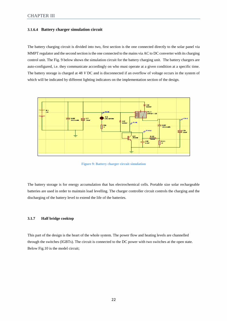
CHAPTER III
22
3.1.6.4 Battery charger simulation circuit
The battery charging circuit is divided into two, first section is the one connected directly to the solar panel via
MMPT regulator and the second section is the one connected to the mains via AC to DC converter with its charging
control unit. The Fig. 9 below shows the simulation circuit for the battery charging unit. The battery chargers are
auto-configured, i.e. they communicate accordingly on who must operate at a given condition at a specific time.
The battery storage is charged at 48 V DC and is disconnected if an overflow of voltage occurs in the system of
which will be indicated by different lighting indicators on the implementation section of the design.
Figure 9: Battery charger circuit simulation
The battery storage is for energy accumulation that has electrochemical cells. Portable size solar rechargeable
batteries are used in order to maintain load levelling. The charger controller circuit controls the charging and the
discharging of the battery level to extend the life of the batteries.
3.1.7 Half bridge cooktop
This part of the design is the heart of the whole system. The power flow and heating levels are channelled
through the switches (IGBTs). The circuit is connected to the DC power with two switches at the open state.
Below Fig.10 is the model circuit;

CHAPTER III
23
Figure 10: Half bridge inverter model
Fig. 10 above shows the model of the cooker. The two switches are switched alternatives to change the DC into high semi-
sine wave frequency alternating current. The two capacitors provide the continuous power flow during the dead time in the
switching.
3.1.7.1 Circuit analysis
The single phase half bridge inverter circuit provides a cheap and easy circuit to construct while also it more
efficient in terms of the energy losses as it only contains two set of switches [29]. The circuits in Fig. 11 below
shows the analysis of the half bridge topology used in the design.
Figure 11: State 1
VS is the DC voltage supply with the two switches connected together. The blue arrows in the figure above show the direction
of current flow during state 1. The blue arrows show that load current is positive and it is supplied by the high side transistor.

CHAPTER III
24
Figure 12: State 2
S1 is switched off, the resonant current flows through and charges or discharges the snubber capacitors and thus
the low side capacitor is discharged while the high side capacitor is charged.
Figure 13: State 3
S1 resonant current starts free-wheeling the low side diode (S2). The load current is still positive.
Figure 14: State 4
S2 is turned on, the load voltage turns negative when the low side transistor is turned on (S2), as it can be seen
by the flow of current (blue arrows).

CHAPTER III
25
Figure 15: State 5
Low side transistor is turned off, load current charges S2 snubber capacitor to supply voltage while S1 snubber
capacitor is discharged simultaneously.
Figure 16: State 6
When both capacitors are charged and discharged the negative load current flows through the high side diode
(S1). When load current approaches zero, the system start again from STATE 1.
3.1.7.2 Snubber Capacitor
The snubber capacitor reduces losses during switching of the transistor. During the on state of the transistor, the
diode is off and all the load current flow in the transistor. When the transistor reaches source voltage, the load
voltage goes to zero. After transistor voltage matches source voltage, diode current increases to load current and
the transistor current goes to zero. As a result, there is a state where both transistor current and voltage becomes
high at the same instance, resulting in a triangular shape instantaneously as seen in the figure below. The snubber
provides another path for the load current. The rate of change of the transistor voltage is minimized by the
capacitor, delaying its voltage from high to low transition.

CHAPTER III
26
Voltage and current during switching Turned off waveform with the snubber capacitor
Figure 17: Snubber circuit
3.1.8 Power flow control circuit
This section is connected together with the user interface. The input for cooking power level is control via buttons
that are connected to the power flow circuit. The user presses any power level on the buttons and the load power
demand analysis is done to make sure if the power selected is available at the time. If the power is not available,
the message will be displayed on the LCD stating the issue or else the selected power will be sent to the half
bridge and displayed in the LCD together with the switching frequency.
3.1.8.1 Design
The design of the half bridge inverter has two important parameters for the design attention needed to be carefully
studied. It is the value of the resonant capacitor tank and the inverter switching frequency.
In the half bridge circuit (RLC), resonance is a result of the collapsing magnetic field of the inductor that generates
an electric current in its windings which charges the capacitor while the discharging capacitor provides and electric
current that builds the magnetic field in the inductor. The resonance occurs at a particular frequency for a given
values of capacitor and an inductor. The highest electrical power and efficiency is produced at this stage of
resonance. The half bridge switching frequency selection is very important and is dependent on the value of the
resonant capacitor and by extension the resonant frequency. The half bridge will operate under zero voltage
switching condition (ZVS). ZVS is when the voltage across the switch is zero when turned on (there will be
current flowing through the body diode of the switch). The above is achieved by switching the half bridge at
frequencies higher than resonant to maintain this state safely.

CHAPTER III
27
Figure 18: Operational range of the half bridge
The Fig. 18 above shows the resonant frequency is the point of maximum power. Frequencies lower than resonant
are in the zero current switching (ZCS) domain. Since capacitors and inductors have the capacity to vary slightly
from their rated values especially during the use, it is necessary to operate in the ZVS territory with some factor
of safety.
The output power, 𝑃ℎ for the harmonic (h) in the inverter can be determined using the Fourier transform as in the
equation below.
𝑃ℎ = 𝑉ℎ,𝑟𝑚𝑠 ∗ 𝐼ℎ,𝑟𝑚𝑠 (6)
Impedance, 𝑍ℎ in the circuit is defined using the equation (7) in fig. 19 below. Where, 𝑅𝑒𝑞is the equivalent
resistance of the pot, the inductive reactance? 𝑋𝑙 = 𝜔𝐿 And the capacitive reactance 𝑋𝑐 = 1
𝜔𝐶 .
Figure 19: Circuit impedance diagram
|𝑍ℎ| = √𝑅𝑒𝑞2 + (𝜔𝐿 −
1
𝜔𝐶)2 (7)
𝜔 = 2𝜋𝑓 (8)
|𝑍ℎ| = √𝑅𝑒𝑞2 + (2𝜋𝑓𝐿 −
1
2𝜋𝑓𝜔𝐶)2 (9)
Current, Iℎ,𝑟𝑚𝑠 in the circuit at harmonic (h):

CHAPTER III
28
𝐼ℎ,𝑟𝑚𝑠 = 𝑉ℎ,𝑟𝑚𝑠
𝑍ℎ (10)
𝐼ℎ,𝑟𝑚𝑠 = 𝑉ℎ,𝑟𝑚𝑠
√𝑅𝑒𝑞2+(𝜔𝐿−
1
𝜔𝐶)2
(11)
The overall equivalent resistance, 𝑅𝑒𝑞 of the circuit can be defined as fellow; Fig. 20 gives the relationship between
the equivalent resistance and switching frequency.
𝑅𝑒𝑞 = 𝑅(𝑓𝑠)𝑓𝑠
𝑓𝑟 (12)
Figure 20: Dependence of resistance on switching frequency
At resonant frequency, the impedance only shows resistive component as the inductive and capacitive reactance
of (7) becomes equal. Therefore the resonant frequency of the circuit can be calculated as below;
𝑓𝑟 = 1
2𝜋√𝐿𝐶 (13)
By manipulating equation (8) using Ohm’s law and by filling in known variables, a solvable equation for the
harmonic (h) power output can be derived (16).
𝑃ℎ = 𝐼ℎ,𝑟𝑚𝑠2𝑥𝑅𝑒𝑞 (14)
𝑃ℎ = 𝑉ℎ,𝑟𝑚𝑠
√𝑅𝑒𝑞2+(𝜔𝐿−
1
𝜔𝐶)2
𝑥𝑅𝑒𝑞 (15)
Σℎ = 1𝑃ℎ =
2𝑅𝑒𝑞𝑉2𝑚𝑎𝑖𝑛𝑠
(ℎ𝜋)2
𝑅𝑒𝑞2+(2𝜋𝑓𝐿−
1
2𝜋𝑓𝜔𝐶)2
(16)
The resistance is selected according to pot material and resonant frequency of the selected choice. The graph in
appendix (B) shows the resistance of the pot material with respect to it resonant frequency. The cast iron material
is selected and the corresponding resistance with respect to the chosen resonant frequency is 1.8 Ω. The iron is

CHAPTER III
29
chosen over aluminium due to a very high resistance at 10 kHz. At 10 kHz aluminum resistance is at 0.2 Ω while
cast iron is 1.82 Ω. The inductance of the coil is chosen to be 99 uH and the resonant capacitance will be calculated
from this value of the inductance using equation below;
𝑓𝑟 = 1
2𝜋√𝐿𝐶
𝐶𝑟 = 2558 𝑛𝐹
Table 3-1 gives the circuit characteristic for the design of the induction coil and the load using resonant estimation
calculation;
Table 3 -1 : circuit parameters
Parameter Definition Calculated value
𝐿𝑒𝑞 Pot coil inductance 99 uH
𝑅(𝑓𝑠) Induction pot resistance +/-1.82 Ω
𝐶𝑟 Resonant capacitor 2558 uF
ℎ Harmonic number 1
𝑓𝑠 Switching frequency at maximum
power
10 kHz
Using equation (12) and (16) the graph below is generated to illustrate how the output power varies with
frequency.
Figure 21: Output power vs. Frequency
Fig. 21 above shows that the peak power is achieved at resonant frequency, 10 kHz. It is important to choose a
frequency a bit greater than resonant in order to approximately achieve zero voltage switching, meaning that the
switch is opened with zero voltage across it. During this switching the circuit will consume 1200 W.
0
500
1000
1500
1 2 10 15 20 20 25 30 35 40 45 50 55 60 65
Switching frequency

CHAPTER III
30
3.1.8.2 Simulation diagram
The advantage of using half bridge is that the high frequency harmonics can be utilized to produce heat in the
coil. The simulation design of half bridge circuit with cooking coil is shown in Fig. 22.
Figure 22: Half bridge inverter with the cooker coil
The half bridge circuit is designed to convert the direct current from PV and mains to alternating current. The half
bridge circuit shown in Fig. 22 is designed using two IGBTs to convert DC into AC. A 48 VDC is fed to the two
IGBTs which are converted to an alternating current by sending opposite PWM signals to the switches. The
amount of voltage created on the coil depends on the switching frequency and the pot material used. The power
ranges from 100W to 600W. L1 and R1 represent the cooker coil and the pot respectively. The four capacitors
shown in Fig. 24 is the resonant tank for continuation of supply during rising and falling of the sine wave. It also
continues to give supply during 2.5 % dead time of the switches in their state change. Voltage and frequency is
controlled by pulse width modulation by changing duty ratio. Simulation graphs for PWM, load current and load
voltage are shown and discussed in chapter V.
3.1.8.3 Control circuit
The flow chart Figure 2of chapter 2 shows the power flow of the system in detail. The chart shows how the
interface responds to the user selection. The system consists of an LCD display to indicate power level and
switching frequency and also gives the system status for any user input. The program in the flow chart first asks
the user to select desired power level. The selected power will send a specific signal to the system and the system
will do a power analysis to check if the battery power is enough to supply the system. If the battery is not enough,

CHAPTER III
31
the system will automatically switched into mains supply. After the cooking is done, the mains will than charge
the battery.
The design consists of two power sources, i.e. solar and mains power. The two power sources are connected
directly to the system. The mains power provides with +/- 230 V and that is converted into direct current via the
converter since the system requires direct current input. The converted DC voltage is 48 V that is able to charger
the battery storage and also be able to independently supply the system. The converter is connected with the first
section of the battery charger control circuit for mains supply charging. The second section of the charging circuit
is the MPPT regulator that is connected to the solar panel, if solar is selected to charge the battery instead of
mains. This means that the battery storage can be charged either by solar or mains power but treating solar a
priority power source. The MPPT is design to regulate the unregulated/ fluctuating DC voltage from the panel.
Two panels of each 300 watts are used to provide a maximum of 600 watts. The user interface with the buttons is
designed for the user to be able to select any power level required. Each power level is programmed with a specific
switching frequency. The switching frequency is controlled by means of the duty ratio. Each complete circle of
the pulse width modulation (PWM) is accommodated with a switching dead time of +/-5 % to allow the switches
not to switch at the same time as this might result in a short circuit. The switching method used is zero voltage
switching (ZVS), i.e. no voltage will be across the switches during the switching. The ZVS is achieved by
switching at frequencies higher than the resonance frequency. The Fig. 23 below shows the overall simulation
circuit of the design.
Figure 23: Whole circuit simulation diagram

CHAPTER III
32
3.2 Conclusion
At this stage, three chapters have been accomplished with success following the general and specific research
objectives. Chapter I was more of a problem statement, including the benefits of solar applications in residential
areas and the rationale for the proposed system for this study by looking at the advantages and disadvantages. The
chapter went even deeper by looking in the general and specific objectives as to meet the design general and
specific expected outcomes. Lastly it discusses about the contribution of the study in the research and also in the
community with the brief arrangement of the thesis chapters at the end. Chapter II concentrates on the existing
technologies relating to the study. The existing literature is studied and analysed accordingly by looking at the
existing gaps and presenting the solutions amongst them. It also touches the design methodology by explain the
circuit or design operation by means of flow diagram. Design stages are also explained in detailed outlining how
the design is handled in terms of achieving general and specific objectives. From the two first chapters, the deep
understanding of the research is achieved by means of generating general and specific objectives and also designs
of the flow chart for power flow together with design stages. Chapter III is more of taking clear understanding
of the research general and specific objectives from chapter I and II into practice by means of mathematical
calculations and circuit analysis of all the design stages together with simulation diagrams. Some blocks in the
block diagram are not simulated in terms making a circuit diagram like auto-switching. The auto-switching feature
is explained by means of flow chart only and will be done using a programmable relay in chapter IV and also the
MMPT regulator will be used to make things more easier for solar to the battery power flow. The following study
is chapter IV, the chapter focuses on the design implementation of the system. And chapter V is the simulation
and practical results obtained using the simulation diagrams in this chapter. It also gives the justifications for
simulations and practical results for each block in the block diagram in section 3.1 of this chapter. Chapter VI is
the thesis conclusion chapter.

CHAPTER IV
33
4 Implementation Design
4.1 Introduction
The schematic below in Fig. 24 shows the actual design diagram for the design implementation. The system
utilizes two power sources, namely; mains and solar as it can be seen below (as per design specification in Chap.1).
The programmable relay is an auto-selection switching that is directly connected with the panel and on the
normally open point (N/O) for the mains to allow auto switching if solar is removed or no enough solar radiation
to make it operate. The MPPT block includes the DC-DC MPPT and AC-DC charger that allows the solar and
mains to charge the batteries respectively. Solar is treated as a priority as per the design specifications discussed
in the previous chapters. The battery bank utilizes the deep cycle batteries for it advantage of slow discharging
and fast charging characteristics. Further analysis is give from section 4.1.1 – 4.1.5. The PCB layout and the
circuit setup can be seen in appendix D.
Figure 24: Implementation design schematic

CHAPTER IV
34
4.1.1 Programmable relay, MPPT and AC-DC charger
Figure 25: Microcare MPPT charger
The MPPT is used in the circuit implementation to easily program and use it for maximum power delivery from
panel as seen in Fig. 25 above. The 20 A MPPT is used to allow it to be able to charger the four 105 Ah batteries
used in the system. The unit is programed to detect battery low at 44 V to avoid draining batteries to low state as
this can cause system low voltages and draw more current to compensate for the output voltage required at a
specific power level and exposed the user to high currents at the output. The factor is that drawing batteries to it
low voltage will shorten the life cycle of the batteries. The unit is integrated with the AC-DC charger and auto-
switch relay to easily communicate as per the code running in the unit. The unit is designed at 500 watts maximum
while the batteries form a 2 kW system and this means that the cooker can run at its maximum power for 4 hours
without charging needed. The MPPT manual can be found on the MICROCARE website.
4.1.2 Battery storage
Figure 26: Battery wiring diagram
The system uses four times 105 Ah, 12 V Dixon deep cycles to make a 48 V system. The image above in Fig. 26
shows the actual battery used together with the wiring diagram on the left as the batteries are connected in series.

CHAPTER IV
35
The batteries present high usage as their discharge gradient is very steep while the charging one is sharp curve.
Safety precaution is followed as the batteries form a huge hazard for the user. The batteries need to be placed in
a cool place, preferable less than room temperature. The batteries also require a recommended carrying during
movement to keep the life cycle as the user out danger as it contains toxic fluids.
4.1.3 Induction cooker
The fig. 27 below shows the main components for the system design;
Figure 27: Cooker diagram
The microcontroller is programmed with eight power levels that are also displayed in the LCD as per the user
selection (see appendix C, Fig. 48 for PCB circuit layout). The user selects any desired power level and a switching
signal is generated at 5 V, get boosted by the IGBT driver to meet IGBT gate to collect switching voltage (12 V)
and then supplied to the switches that is connected to 48 V DC bus voltages and convert it to AC to run the cooker.
The results for all the switching power levels are show in the results section Figure (38-45) of chapter 5. Arduino
microcontroller is the preferred choice due to it affordability, easy to program and having open source libraries
that includes LCD. The common ground is shown to emphasize the importance that can affect the whole setup if
not connected properly.
4.1.4 Driver circuit
The IGBT driver circuit plays a big role in the circuit operation. The drive acts as a voltage isolator between microcontroller
and the DC bus voltage. It also boosts the input signal to a recognized switching voltage in the IGBTs. The circuit diagram
can be seen on appendix (B) Figure 46. International rectifier driver is used (IR2184). The offset voltage is 600 V with fast
turn off/on times that makes them to quickly distort the signal as soon as possible. It also presents short dead time that allows
greater power transfer to the load. The driver uses 1 uF decoupling capacitor to reduce voltage spikes that might
damage the circuit. The 100 nF is a bootstrap capacitor that act as a charge pump to switch the IGBTs.

CHAPTER IV
36
4.1.5 Half bridge
The half bridge circuit consists of high and low side IGBT, inductor coil, pot and resonant capacitors. IGBTs were
used instead of the MOSFETS due to its Ability to handle the high voltage (600V), low conduction and due to the
frequency (10-65 kHz), IGBTs forms better option. This circuit utilizes the G4PC50F IGBT. This component
was chosen due to its ultrafast switching, high input impedance, low conduction losses and low switching losses.
The SGL160N60UFD IGBT is used in the circuit. The resonant capacitors are placed in parallel on either side of
the load. Four 270nF used rather than two 540nF capacitors because high value capacitors have poor high
frequency response properties and exhibit a high series parasitic resistance.
Figure 28: Half bridge inverter
The resistance Located in series between the driver signal and the IGBT gate in Fig. 28 above is a potentiometer.
This acts as a gate resistor and limits the instantaneous current that is drawn when the IGBT is turned on it
functions as a slew-rate limiting device for the gate signal, reduces ringing and voltage spikes. The IGBTs are
mounted on a heat sink, which dissipates waster heat generated during switching into the surrounding air. An
insulating pad and thermally conductive paste lie between the IGBTs and the heat sink. The insulating pad
combines a film and silicone rubber and acts as a tough dielectric barrier against cut-through.
4.2 Circuit performance

CHAPTER IV
37
The induction cooker was implemented with success and is capable of generating enough heat. The Fig. 29 below
shows the circuit performance during testing. The system uses one supply of 48 V DC to power all the circuits, 5
V for microcontroller and LCD, 12 V for IGBT drivers. All the input and output power parameters are displayed
in chapter 5 (Table 5-17) together with each level output efficiency. The cooker was tested using water of about
700ml. The cooker managed to heat the water at approximately 100 °C from power level 5 upwards and this is
due to the amount of power consumed by the load at the time. The water actually needs more energy to heat from
90 to 100 °C as more stronger bonds require sufficient energy to latent heat to convert liquid state to gas form.
Figure 29: Induction cooker, pot, and whole setup

CHAPTER V
38
5 System Simulations and Practical results
5.1 Introduction
Induction cooker presents the most efficient way of cooking compared to the traditional cooking methods that are
high in the market. The cooker also come with energy savings, cleanness and quicker in power delivering within
seconds to reach maximum output as stipulated in chapter II and III. The solar powered cooker it even adds more
on the power and money savings as explained in details in the previous chapters. The schematic and mathematical
design in chapter III showed a proper circuit analysis together with necessary calculations to prove the feasibility
of the solar powered induction cooker. The code can be seen in appendix (D) that runs in the background of the
simulations and practical of the system. The code control the alternative switching of the two half-bridge IGBTs
and work to display the power level and switching frequency. This chapter presents the simulation results gathered
in the design and simulation circuits in chapter III. It also shows the corresponding practical results. Some of the
circuits in the block diagram are not simulated but are shown in the practical results section to complete the design.
Each simulation and practical result shows the pulse width modulation, load current and voltage. The output power
is calculated using the load current and voltage. The current generated at the output is highly dependent on the pot
material used during simulations and or practical. The simulations are shown and explained in section 5.2 followed
by experimental results in section 5.3, results analysis in section 5.4, adjustments made to accommodate
implementation of the design prototype together with proper justifications made from the simulations Section 5.5,
circuit analysis in section 5.6 and future work in section 5.7. This chapter answers all the previous chapters by
meeting general and specific objectives of the design and also answers the aim of the research. This is the core
chapter of the study. The discussion at end of this chapter touches how this research meet the commercial product
standards together with future research in the same study and how it can be improve from what has been done.
5.2 Simulation results
The simulation results for selection of various power levels are shown in Figures 30 to 37 together with power
consumed in Table 5-1 to 5-8. The simulation design is tested using Proteus software. The results include pulse
width modulation, current in the coil and the load voltage in the presence of the pot. The results differ with
switching frequency. The frequency ranges from 10 kHz to 65 kHz. The simulations are carried out using one pot
resistance value of 1.23 ohms as load. It is noted that changing the pot material can negatively or positively affect
the output power keeping voltage and frequency constant. The higher the resistance the higher the output power
and vice versa. The results shows simulations for all eight power levels as indicated in the design specific
objectives in chapter I and II.

CHAPTER V
39
The Fig. 30 below shows power level one in a form of three waveforms, pulse width modulation frequency
(PWM), load voltage and current respectively. The PWM switching signal is modelled in Proteus as mentioned
above creating a pulse voltage of 5 V to drive the two half bridge IGBTs alternatively to allow it not to switch at
the same time. 5 V is only able to drive the switches in the simulation as the IGBTs are ideally and no need of the
driver circuit to amplify the signal. The two PWM signals yellow (high-side) and blue (low-side) has a dead time
of about 5 – 10 % per cycle to allow smooth switching. It can be noted that there is a small distortion in the PWM
but with no measure effects in the driving of the inverter circuit. The noted distortion can result in a temperature
rise in the IGBTs. This will be dealt with correct with the use of the isolators and trimmers to make it smooth in
the implementation section 4. The voltage and current are almost sinusoidal with a peak voltage of 60 V and peak
current of 6 A. Fig. 30 is further followed by Table 5-1 that represent the RMS values of the source and load
currents and voltages to get the actually power supplied and consumed at power level one. The efficiency of the
system is behaving ideally as expected due that no real components with different tolerances to contribute to
external losses. Thus the results in the Fig. 30 and Table 5-1 are expected to differ in the practical stage. All the
other following power levels from Fig. 31 – 37 have a similar trend to the current Figure but differ slightly and
all the differences will be mentioned in all the Figures.
Table 5 -1: power level one result
PWM Level one 62.5 kHz
Load voltage 60 V
Load current 6 A
Figure 30: Power level one
Inputs Outputs
VRMS 48 V VRMS 42.43 V
IRMS 3.98 A IRMS 4.24 A
PIN 191.04 W POUT 180 W
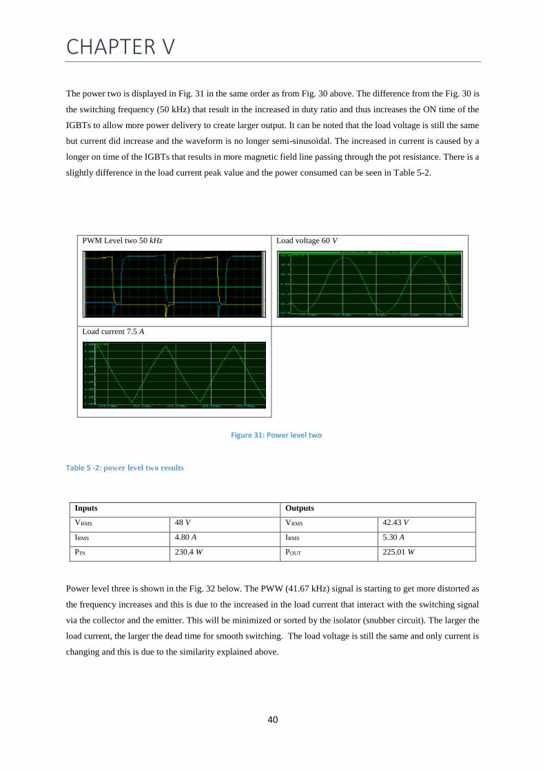
CHAPTER V
40
The power two is displayed in Fig. 31 in the same order as from Fig. 30 above. The difference from the Fig. 30 is
the switching frequency (50 kHz) that result in the increased in duty ratio and thus increases the ON time of the
IGBTs to allow more power delivery to create larger output. It can be noted that the load voltage is still the same
but current did increase and the waveform is no longer semi-sinusoidal. The increased in current is caused by a
longer on time of the IGBTs that results in more magnetic field line passing through the pot resistance. There is a
slightly difference in the load current peak value and the power consumed can be seen in Table 5-2.
Table 5 -2: power level two results
Inputs Outputs
VRMS 48 V VRMS 42.43 V
IRMS 4.80 A IRMS 5.30 A
PIN 230.4 W POUT 225.01 W
Power level three is shown in the Fig. 32 below. The PWW (41.67 kHz) signal is starting to get more distorted as
the frequency increases and this is due to the increased in the load current that interact with the switching signal
via the collector and the emitter. This will be minimized or sorted by the isolator (snubber circuit). The larger the
load current, the larger the dead time for smooth switching. The load voltage is still the same and only current is
changing and this is due to the similarity explained above.
PWM Level two 50 kHz
Load voltage 60 V
Load current 7.5 A
Figure 31: Power level two

CHAPTER V
41
Figure 32: Power level three
Table 5 --3: Power level three results
Inputs Outputs
VRMS 48 V VRMS 42.43 V
IRMS 7.80 A IRMS 8.48 A
PIN 374.40 W POUT 360.03 W
Power level 4-6, Fig. 33-35 have a similar trend of increased in switching frequency, same load voltage and more
similar load current waveform but increasing in peak to peak value. This is due to that these frequencies are now
closer to resonance frequency as seen in Fig. 18 of chapter 3. It can be seen from the mentioned figures how the
distortion changes and how the load current is changing as well. All the analysis is done using one pot resistance.
PWM Level three 41.67 kHz
Load voltage 60 V
Load current 12 A

CHAPTER V
42
Figure 33: Power level four
Table 5 --4: Power level four results
Inputs Outputs
VRMS 48 V VRMS 42.43 V
IRMS 8.30 A IRMS 9.19 A
PIN 398.40 W POUT 390.03 W
Figure 34: Power level five
PWM Level four 35.71 kHz
Load voltage 60 V
Load current 13 A
PWM Level five 27.78 kHz
Load voltage 60 V
Load current 15 A

CHAPTER V
43
Table 5 -5: Power level five results
Inputs Outputs
VRMS 48 V VRMS 42.43 V
IRMS 9.50 A IRMS 10.60 A
PIN 456.0 W POUT 450.03 W
It is noted that power level 6 (Fig. 35) is the same as power level due to that their frequency lie in side and thus
contribute to the same power level.
Figure 35: Power level six
Table 5 -6: Power level six results
Inputs Outputs
VRMS 48 V VRMS 42.43 V
IRMS 8.30A IRMS 9.19 A
PIN 398.4 W POUT 390.03 W
Fig. 36 shows the second to last power level at 15.15 kHz. The duty ratio can be noticed increasing even further
at this switching stage. The dead time is a bit small and high power is produced at this stage. This switching signal
lies almost around the resonance. The load voltage is also increased slightly and that is caused by the change
inductance as the approaching resonance. The RMS values are stipulated in Table 5-7.
PWM Level six 20 kHz
Load voltage 60 V
Load current 13 A

CHAPTER V
44
Figure 36: Power level seven
Table 5 -7: Power level seven results
Power level 8 below in Fig. 37, shows a very high voltage shoot as results of resonance. Equation (10) in chapter
III shows a great relationship between inductance and capacitance. At resonance, capacitive and inductive
reactance’s re approximately the same and thus can expect a huge rise and RMS voltage as a result. Load voltage
is peaking at 180 V. For the induction cooker, it is not expected to have such big power consumed by the load.
This is happening just because the simulations source is not limited in terms of how much the load is expected to
draw. The maximum power is expected to be around 500 watts for the cooker as almost more than 80 % of the
power is converted to cooking and thus require less power.
PWM Level seven 15.15 kHz
Load voltage 65 V
Load current 14 A
Inputs Outputs
VRMS 48.0 V VRMS 45.96 V
IRMS 9.60 A IRMS 9.89 A
PIN 460.80 W POUT 454.98 W

CHAPTER V
45
Figure 37: Power level eight
Table 5 -8: Power level eight results
5.3 Experimental results
The practical results are shown below from Fig. 38-45 together with the power that is consumed in Table 5-9 to
5-16 during operation. The results shows the PWM with different switching frequency, which goes with load
current and voltage to show power that is consumed by the load during operation. The results were taken in Durban
at Tower residence the University of Kwa-Zulu Natal.
Figure 38 shows the practical results of power level one for the induction cooker testing. The testing was
performed using oscilloscope to capture all the readings. The signals were taking using a smart phone device. This
figure below was expected to give same results as of Fig. 30 in the simulation results. The first challenge was that,
the simulations were using an unlimited source that was not controlled in terms of how much the circuit is going
to draw at a specific frequency. Frequency was the only controlled variable during the simulations and practical.
It is not possible to use an unlimited source in the practical section as this can course burning issues in the circuit
PWM Level eight 10 kHz
Load voltage 180 V
Load current 12 A
Inputs Outputs
VRMS 48 V VRMS 127.28 V
IRMS 22.80 A IRMS 8.49 A
PIN 1094.40 W POUT 1080 W

CHAPTER V
46
and as for safety of the user, testing purposes; the 500 watts power supply was used. The waveform signals are
similar, though the actual peak values differ as adjustments were made in terms limited component usage. The
Table 5-9 gives the RMS values for input and output parameters to calculate power consumed, together with its
efficiency as indicated in Table 5-17 at the end of this chapter.
PWM Level one 62.5 kHz
Load voltage 32.5 V
Load current 5 A
Figure 38: Power level 1
Table 5 -9: Power level one result
Input (s) Output (s)
VRMS 49.9 V VRMS 22.98 V
IRMS 2.40 A IRMS 3.54 A
PIN 119.76 W POUT 81.25 W
From Fig.39, it can be noted that in the practical section, the current remains the same for power level 1 and 2 and
only the load voltage that is changing. This is due to the resonant capacitors used in the practical which can take
more current spikes from the induction coil and give a smooth larger voltage instead of high current for such low
power stages. It can also be seen the load voltage signal is a bit distorted, which is caused by the increased in
voltage.

CHAPTER V
47
PWM Level two 50 kHz
Load voltage 50.12 V
Load current 5 A
Figure 39: Power level two
Table 5 -10: Power level two results
Input (s)
Output (s)
VRMS 48.90 V VRMS 35.44 V
IRMS 3.2 A IRMS 3.54 A
PIN 166.26 W POUT 125.30 W
Figure 40 shows the practical results for power level 3. The value of the load current is still constant as for the
reason explained above. The load voltage and switching frequency are the only parameters changing. The Table
5-11 gives the actual RMS values and power consumed by the load at the time. The dead time was programmed
per each power level as to meet correct switching characteristics.
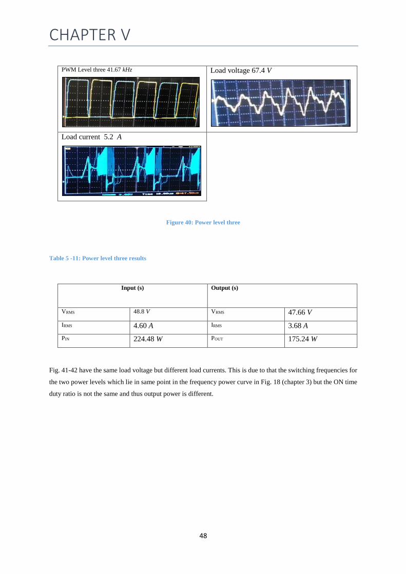
CHAPTER V
48
PWM Level three 41.67 kHz
Load voltage 67.4 V
Load current 5.2 A
Figure 40: Power level three
Table 5 -11: Power level three results
Input (s)
Output (s)
VRMS 48.8 V VRMS 47.66 V
IRMS 4.60 A IRMS 3.68 A
PIN 224.48 W POUT 175.24 W
Fig. 41-42 have the same load voltage but different load currents. This is due to that the switching frequencies for
the two power levels which lie in same point in the frequency power curve in Fig. 18 (chapter 3) but the ON time
duty ratio is not the same and thus output power is different.

CHAPTER V
49
PWM Level four 35.71 kHz
Load voltage 78.2 V
Load current 5.5 A
Figure 41: Power level four results
Table 5 -12: Power level four results
Input (s)
Output (s)
VRMS 48.60 V VRMS 55.15 V
IRMS 5.40 A IRMS 3.90 A
PIN 262.44W POUT 215.09 W
PWM Level five 27.78 kHz
Load voltage 78.2 V
Load current 7.3 A
Figure 42: Power level five

CHAPTER V
50
Table 5 -13: Power level five results
Input (s) Output (s)
VRMS 48.50 V VRMS 55.15 V
IRMS 6.70 A IRMS 5.16 A
PIN 324.95 W POUT 284.68 W
It is noted that Fig. 43-45 have the same load voltage but differ in load currents. This is due to more magnetic
field line entering the pot at a time and results in a rise in the load current in the pot. Remember, current generated
at the load depends directly on the load resistance and switching frequency. It is also noted that efficiency increases
with the increase in power levels as fast switching is adapted. Table 5-14 to 5-16 shows the actual RMS values
of the input and output parameters.
Figure 43: Power level six
Table 5 -14: Power level six results
Input (s) Output (s)
VRMS 48.30 V VRMS 66.75 V
IRMS 7.1 A IRMS 4.60 A
PIN 342.93 W POUT 306.80 W
PWM Level six 20 kHz
Load voltage 94.4 V
Load current 6.5 A

CHAPTER V
51
PWM Level seven 15.15 kHz
Load voltage 94.6 V
Load current 7.5 A
Figure 44: Power level seven
Table 5 -15: Power level seven results
Input (s) Output (s)
VRMS 48.10 V VRMS 66.75 V
IRMS 8.2 A IRMS 5.30 A
PIN 394.42 W POUT 353.99 W
Figure 45: Power level eight
PWM Level eight 10 kHz
Load voltage 94.9 V
Load current 9.1 A

CHAPTER V
52
Table 5 -16: Power level eight results
Input (s) Output (s)
VRMS 48.05 V VRMS 66.75 V
IRMS 9.8 A IRMS 6.44 A
PIN 470.40 W POUT 429.51 W
5.4 Results Analysis and Discussion
5.4.1 Simulations vs. Practical
The Table 5-17 below shows the input and output parameters for both simulations and practical results. The peak
values from Fig. 38-45 are converted to root mean square to get the actual current and voltage in order to get
power and efficiency for each power level. It can be noted that as the frequency decreases (from low power); the
power output is increased simultaneously and vice versa. The table below indicates cooker switching power levels
from low to high power level respectively. It can be seen that the efficiency increases with increased in switching
frequency and that means lower power frequencies are less efficient than the ones closer to resonant. Low
efficiency in power level 1-3 is caused by the huge losses in the IGBT as the switching is a bit slower compared
to the rest of the power levels. There is a study of dual-mode in induction heating that discusses about the induction
heater with two half-bridge inverters. It is classified as class D and DE for high and low power output range
respectively. The combination of the two operating modes of the classes achieves high efficiency for a wide range
of power output [31].
5.4.2 Circuit Performance
5.4.2.1 Efficiency
The implemented system is a 500 watts supply. All the power dissipation of the important components was
measured using 500 watts operating power. The losses can be of IGBT, diode, filter and coil. These losses are
estimate that the cooker efficient is expected to be around 80 %. The efficiency of the cooker is tested to determine
its performance. Equation (17) below is used to determine efficiency of the system using input and output
parameters as seen in the table 5-17 below.
ζ = (1 − (𝑃𝑖𝑛−𝑃𝑜𝑢𝑡
𝑃𝑖𝑛)) × 100 (17)
Table 5-1 shows the circuit characteristics of the system of the cooker from power level 1-8 respectively. The
switching frequency ranges from 62.5- 10 kHz. It can be seen that the simulation system efficiencies ranges above

CHAPTER V
53
90 % while the practical starting at about 67 % up to 91 %. This is caused by the low switching signals that result
in too many losses in the IGBTs. These power levels from 1-3 as seen in the figure below are probably the one
used in commercial induction cooking applications as great system settings that can be used for a longer period.
But those efficiencies can be improved further with the application of dual mode discussed earlier. Power level 4-
8 efficiencies ranges from 80 - 90 %. These are very encouraging and it is due to the following reasons; using
only half-bridge (2 IGBTs), safe dead time, running the cooker close to resonance frequency. The sharp drop in
efficiency is caused by the system losses explained in paragraph 1 of this section.
Table 5 -17: Simulations and practical results overview
Simulation results
Practical results
Input (s) Output (s)
Input
(s)
Output (s)
Vin 48 V Vout 42.43 V Vin 49.9 V Vout 42.43 V
Iin 3.98 A Iout 4.24 A Iin 2.40 A Iout 4.24 A
Pin 191.04 W Pout 180 W Pin 119.76 W Pout 180 W
ξ 94.22 % ξ 67.84 %
Power level one
Vin 48 V Vout 42.43 V Vin 48.90 V Vout 35.44 V
Iin 4.80 A Iout 5.30 A Iin 3.2 A Iout 3.54 A
Pin 230.4 W Pout 225.01 W Pin 166.26 W Pout 125.30 W
ξ 97.66 % ξ 75.36 %
Power level two
Vin 48 V Vout 42.43 V Vin 48.8 V Vout 47.66 V
Iin 7.80 A Iout 8.48 A Iin 4.60 A Iout 3.68 A
Pin 374.40 W Pout 360.03 W Pin 224.48 W Pout 175.24 W
ξ 96.16 % ξ 78.06 %
Power level three
Vin 48 V Vout 42.43 V Vin 48.60 V Vout 55.15 V
Iin 8.30 A Iout 9.19 A Iin 5.40 A Iout 3.90 A
Pin 398.40 W Pout 390.03 W Pin 262.44 W Pout 215.09 W
ξ 97.98 % ξ 81.95 %
Power level four
Vin 48 V Vout 42.43 V Vin 48.50 V Vout 55.15 V

CHAPTER V
54
5.5 Simulation and Practical results comparison and justification
Section 5.2 to 5.3 shows the results for the simulations and practical respectively. For the practical, 1.01 Ω pots
was used for demonstration and that affect the results as power generated in the load depends on the coupling pot
with the inductor. There are some changes that where adapted in order to meet practical circuit implementation
and testing. See appendix C for simulation, practical results together with system efficiency for each power level.
Below is the list of changes made to accommodate design implementation;
105 Ah batteries used instead of the 25 Ah proposed to accommodate system stability.
IGBT driver circuit used to meet IGBT collector to emitter switching voltage.
The pot resistance use in the theoretical calculations is slight bigger than the one use in the practical and
that brings large power difference.
The power supply is designed at 500 watts maximum and it can only produce up to maximum as this is
a prototype to demonstrate the working principle of the idea. To also reduce chances of being exposed
to high current that might result in injuries during building and testing.
Iin 9.50 A Iout 10.60 A Iin 6.70 A Iout 5.16 A
Pin 456.0 W Pout 450.03 W Pin 324.95 W Pout 284.68 W
ξ 98.68 % ξ 87.60 %
Power level five
Vin 48 V Vout 42.43 V Vin 48.30 V Vout 66.75 V
Iin 8.30A Iout 9.19 A Iin 7.1 A Iout 4.60 A
Pin 398.4 W Pout 390.03 W Pin 342.93 W Pout 306.80 W
ξ 97.98 % ξ 89.70 %
Power level six
Vin 48.0 V Vout 45.96 V Vin 48.10 V Vout 66.75 V
Iin 9.60 A Iout 9.89 A Iin 8.2 A Iout 5.30 A
Pin 460.80 W Pout 454.98 W Pin 394.42 W Pout 353.99 W
ξ 98.69 % ξ 89.75 %
Power level seven
Vin 48 V Vout 127.28 V Vin 48.05 V Vout 66.75 V
Iin 22.80 A Iout 8.49 A Iin 9.8 A Iout 6.44 A
Pin 1094.40 W Pout 1080 W Pin 470.40 W Pout 429.51 W
ξ 98.72 % ξ 91.30 %
Power level eight
CHAPTER V
55
The mains AC to DC converter / charger is no longer connected direct to the cooker but both the solar
and the mains are to charge the battery bank to completely make the cooker a standalone product that
only work with the batteries.
A lot of assumptions were made to meet the design general and specific objective.
5.6 Circuit results analysis
The aim of this section is to analyse the system operating characteristics. The analysis covers the evaluation of
the achievements from solar panel, mains, MPPT up to inverter and induction cooker and the system strength and
weaknesses.
5.6.1 Achievement
The design and the manufacture of the AC to DC 48 V charger went very well as per the design
specifications in chapter 1.
The design and the programming of the MPPT regulator were tested and work successfully.
The integration of the mains and the solar via programmable relay with as per the general and specific
requirements.
The automatic switching went well as well and demonstrated the feature of auto-switching and taking
solar as a priority.
The battery storage is charging perfect in both the power sources.
The main part of design, the cooker performed absolutely fantastic of which is way better than was
expected.
All the design specifications in general and specific objectives were met, though maximum design power
output for the prototype was different from what was used in the simulations.
5.6.2 Strengths
The cooker successfully heated the pot using the principle of electromagnetic induction by varying
switching frequency.
The components to construct the cooker are very few, cheap and affordable.
The efficiency is very encouraging from power level three upwards and this will prolong the life cycle
of the components used and decrease cooling requirements and expenses.
Battery tank can run the cooker at it maximum for about 6 hours with charging needed.

CHAPTER V
56
The cooker output power levels and its efficiency is comparable and can compete with the commercial
cookers in the market. This analysis was tested and proven by comparing the electric stove, commercial
cooker and this cooker I have designed with the advantage of being flexible in terms of power sources.
The system can also run the whole house lighting, charge cell phones, play radio and television at the
same time if proper inverter is connected in the system.
5.6.3 Weakness
The switching PWM from the microcontroller must be applied first to the IGBT gates before the 48 V
can be switched on due to frequency bouncing and that can damage the IGBT straight away by shorting
the emitter and the collector.
The second drawback comes with low efficiencies at low power levels which fail to heat water up to its
boiling point.
High power levels cannot run for too long, like more than 30 minutes as IGBTs get hot and damaged
after some time. This can be fixed by getting good PWM signal trimmers to minimize spikes in the
switching signal.
The confident shows that the minor drawbacks can be sorted provide that necessary alterations are done
to 100 % meet the general and specific objectives.
CHAPTER VI
57
6.1 Conclusion
The induction cookers in the market use mains power to operate of which limits the flexibility in terms of power
sources. The working principle of the project is similar to what is in the literature, but with more of advancement
features using auto selection in terms power sources, taking solar as a priority with the addition of battery storage
as a backup and also to make it a complete portable standalone product. The benefits includes, economic of which
the energy is free from sun, environmental looks at zero released of toxic gases in the atmosphere and health in
terms decreasing the amount of fossil fuels usage. The cookers in the market are completely dependent into
electricity generated by Eskom. The introduction of solar energy comes with the aim of filling the big gap existing
amongst the use of electricity that is 100 % dependent on non-renewable resources. It is also working in line with
the sustainable development plan from department of energy. 98 % of the literature study proves that almost all
the stoves in the market from electric, gas and induction cookers depends on non-renewables resources to operate.
There is only one paper discussing about solar induction cooker but lacking a lot of advancement as it is a very
low power, low efficiency and not flexible in terms of power sources as the country still run with non-renewables.
This makes the paper to not compete with the cookers in the market. The general and specific objection of the
smart solar powered induction cooker were met though they were some slightly adjustments made to
accommodate the implementation as explain in chapter 4. All the design stages explained in chapter 2 were
followed and met. The arrangement of the thesis is done in the form of chapters 1-6 of which are classified in
specific topics given per chapter. This research was done following proper scientific processes including all the
aspects including studying the design and following the right methods as form of presenting quality of research.
The design is proven to meet the commercial standards as explained in chapter 4 of which brings a very big
completion. The only factor to note is that installing the product is expensive (see Appendix C, Table C-1 and 2)
though the costs can be recovered in about 4-5 years’ time and make massive saving. The system can manage to
run the whole house appliance of a small family home and can be adjusted accordingly to meet user requirements
as per the appliances in the house. It is proven as from (Appendix C, Table C-3) using the power estimation that
running a 2 plates electric stove with a consumption of 1.5 kW can take about 8 kW in 4 hours’ time, while the
induction cooker can run at one third of 1.5 kW and still produce efficient results taking only 2 kW in 4 hours.
The system is proven to provide savings at about more 50 % for cooking purposes and about 70 % if all the
appliances like television, radio, lights, charging cell phone and etc. can be integrated with the system.

CHAPTER VI
58
6.2 Future work
There is a number of modifications that can be done in the project in order for it to be further developed as per
below;
Design a circuit to trim the voltage spikes in the PWM signals to reduce IGBT from heating.
Use a bigger microcontroller with more pins like atmega32 to have enough pins for all the circuit
programing as reset button is used to clear the signal after every switching done.
Design and add a dual mode half bridge to improve the efficiency of the circuit as discussed in chapter
4.
The other feature can be to design a pot detection circuit as the circuit cannot work without the pot being
present.
The system is capable of running cooker, house lighting, and television, charging cellphones (Put
inverter) and running other small power consuming devises. This can bring lots of benefits for the user
in decreasing the electricity bills even more.

59
References
[1]S. Villacís, J. Martínez, A. Riofrío, D. Carrión, M. Orozco and D. Vaca, "Energy Efficiency Analysis of
Different Materials for Cookware Commonly Used in Induction Cookers", Energy Procedia, vol. 75, pp. 925-
930, 2015.
[2] J. Acero et al., "The Domestic Induction Heating Appliance: An Overview of Recent Research," In Proc. Appl.
Power Electron. Conf Expo, 2008.
[3] Carlos Sagues Blazquiz and Gonzalo Lopez-Nicolas, "Reset observers and temperature control for induction
hobs," Universidad de Zaragoza, Spain, Zaragoza, Phd Thesis 2254-7606, 2011.
[4] D. C. Jiles and D. L. Atherton, "Theory of ferromagnetic hysteresis," Journal of Magnetism and Magnetic
Materials, 1986.
[5] Sadhu, Pradip Kumar, et al. "A Comparative Survey on High Efficient Clean Heat Production through
Microwave Oven and Induction Cooker."
[6] C.Ekkaravarodome, P. Charoenwiagnuea, K. Jirasereeamornkul, “The Simple Temperature Control for
Induction Cooker based on Class-E Resonant Inverter”, 2013 IEEE 10th conference on Electrical Engineering,
Electronics, Computer, Telecommunications and Information Technology (ECTI-CON), pp 1-6, May 2013.
[7] ENERGY, ON RENEWABLE. "WHITE PAPER ON RENEWABLE ENERGY." (2003).
[8] Asmarashid Ponniran , Abdul Fatah Mat Said “DC-DC Boost Converter Design for Solar Electric System”
International Conference on Instrumentation, Control & Automation ICA2009, ISBN 978-979-8861-05-5 pp-210-
214.
[9] Cerri, Graziano, et al. "Rigorous electromagnetic analysis of domestic induction heating appliances." PIERS
Online 5.5 (2009): 491-495.
[10] Lucia, Oscar, et al. "Efficiency-oriented design of ZVS half-bridge series resonant inverter with variable
frequency duty cycle control." IEEE Transactions on Power Electronics 25.7 (2010): 1671-1674.
[11] Bhavana Ffion, Faseen.K., and Hema Mohan, “Solar Based Induction Cook Top”, 3rd Int. Conf. on
Electronics, Biomedical Engineering and its Applications (ICEBEA'2013) April 29-30, 2013, Singapore.
[12] Chun-Liang, H., 2007, July. Circuits analysis of inductive heating-device with half-bridge resonated inverter.
In 11th WSEAS Int. Conf. Circuits (pp. 26-30).
[13] Sweeney, Micah, et al. "Induction Cooking Technology Design and Assessment." Small 5 (2014): 800.

60
[14] Anis, Priya, et al. “Customer’s Attitude and Satisfaction of Induction (cook-tops) stove in Tirunveli City.”
IRACST 5.1 (2016): 2319-2828
[15] Agarwal, Paul D., "Eddy-current losses in solid and laminated iron," American Institute of Electrical
Engineers, Part I: Communication and Electronics, Transactions of the , vol.78, no.2, pp.169,181, May 1959.
[16] Dodd, C. V., “Some eddy-current problems and their integral solutions,”Oakridge National Laboratories,
April 1969.
[17] Llorente, S.; Monterde, F.; Burdio, J.M.; Acero, J., "A comparative study of resonant inverter topologies used
in induction cookers,"Applied Power Electronics Conference and Exposition, 2002. APEC 2002.Seventeenth
Annual IEEE, vol.2, no., pp.1168, 1174 vol.2, 2002.
[18] Meng, L.C., Cheng, K.W.E. and Chan, K.W., 2009, May. Heating performance improvement and field study
of the induction cooker. In Power Electronics Systems and Applications, 2009. PESA 2009. 3rd International
Conference on (pp. 1-5). IEEE.
[19] Forest, F., Laboure, E., Costa, F. and Gaspard, J.Y., 2000. Principle of a multi-load/single converter system
for low power induction heating. IEEE Transactions on Power Electronics, 15(2), pp.223-230.
[20] Semiconductor, O., 2014. Induction Cooking Everything You Need to Know. Phoenix, Estados Unidos,
AND9166/D.
[21] A. Zahedi, “energy, People, Environment, Development of an integrated renewable energy and energy
storage system, an uninterruptible power supply for people and for better environment,” The International
Conference on Systems, Man, and Cybernetics, 1994.
[22] Viorel B. Modeling solar radiation at the earth's surface: Recent advances. Springer. 2008. ISBN:
3540774548.
[23] S. Pyakuryal and M. Matin “Implementation of AC to DC Converter using Thyristor in ATP,” IOSR Journal
of Engineering; vol. 2, Issue 11, pp. 06-11, November 2012.
[24] J. Doval-Gandoy, C. Castro, and M. C. Martinez “Line Input AC to DC Conversion and Filter Capacitor
Design,” IEEE Trans. Industry Application; vol. 39, no.4, pp. 1169-1176,July/August 2003.
[25] M. H. Rashid, Power Electronics Handbook. Massachusetts: Academic Press, 2007, Chap. 10.
[26] Linden, David, and Thomas B. Reddy. "Handbook of Batteries. 3rd." (2002).
[27] Joseph, Ami, and Mohammad Shahidehpour. "Battery storage systems in electric power systems." Power
Engineering Society General Meeting, 2006. IEEE. IEEE, 2006.
[28] Distillation, Solar. "Practical Action Technology Challenging Poverty." Accessed on 26.07.
[29] S. Llorente, F. Monterde, J. M. Burdio, and J. Acero, "A Comparative Study of Resonant Inverter
Topologies Used in Induction Cookers," University of Zaragoza, Zaragoza.

61
[30] Semiconductor, O., 2014.The Effect of Pan Material in an Induction Cooker. Denver, Colorado,
AND9201/D
[31] H. Sarnago, O. Lucia, A. Mediano, and J. M. Burdio, "Dual-Mode-Operation Half-Bridge Resonant
Converter for Improved-Efficiency Induction Heating System," Department of Electronic

62
Appendix A
AC to DC converter calculations
𝑉𝑑𝑐 == 2.220𝑉
𝜋 2. 𝑉𝑠
𝜋= 140 𝑉
The DC voltage is 140 volts while the expected is 80 volts DC. The transformer is used to give the ratio in order
match the required DC voltage. The ratio is 220 / 80 and that is 2.75. Using the calculated ratio;
𝑉𝑑𝑐 = 2.80
𝜋= 50.93 𝑉
The second calculation is the expected load voltage using eq.3;
𝑉𝐿 = 𝑉𝑠
√2=
80
√2= 56.57 𝑉
The load voltage is 56.57 volts and the 48 volts DC to DC voltage IC is used to regulate the DC value to the
required output. The 230V 3 A mains socket is used to power the circuit. The DC and load current are calculated
below;
𝐼𝑑𝑐 = 2. 𝑉𝑠
𝜋. 𝑅𝐿
= 2.80𝑉
𝜋. 5𝑜ℎ𝑚 = 10.19 𝐴
𝐼𝐿 = 𝑉𝑠
√2. 𝑅𝐿
= 80
√2. 5= 11.31 𝐴
The load resistance is assumed at 5 ohms. The DC and load current are 10.18 A and 11.31 A respectively. Using
the above calculations, the expected load power is calculated below;
𝑃𝐿 = 𝑉𝐿 . 𝐼𝐿 = 56.57. 11.31 = 639.81 𝑊
And using 48 V DC the power is 542.88 W.

63
Appendix B
Pot resistance vs. switching frequency
Figure 46: Equivalent series resistance for aluminium and cast iron [30]

64
Appendix C
Practical and design cost
Figure 47: Power unit and deep cycle battery

65
Figure 48: Whole circuit PCB layout

66
Figure 49: Driver circuit operational diagram
Table C-2: Induction cooker components
Component (s) Part number Quantity (s) Price (Rands)
Capacitors MKP270 4 10.00
IGBTs SGL160N60UFD 2 90.00
potentiometer 2k 2 10.00
Decoupling caps 100nF 2 3.00
Atmega 328 1 40.00
LCD 20 x 2 1 80.00
heatsinks Heatsink 1 20.00
Coil 99.5 uH 1 20.00
R273.00
Table C-2: other components for complete solar system unit
Component (s) Part number Quantity (s) Price (Rands)
Batteries Dixon DC 105ST
12V
4 20 700.00
Whole PSU comp 500 W 48V DC 1 11 900.00
Solar panels SOL310-RNW 2 9 500.00
R 42 100.00
Table C-3: Electric stove (2 plates) consumption

67
Appendix D
Code for the whole circuit operation
#include <LiquidCrystal.h>
#include <PWM.h>
#include <Wire.h>
// initialize the library with the numbers of the interface pins
LiquidCrystal lcd(12, 11, 7, 4, 3, 2);
float voltage = 0.0;
int powerSource = 0;
int led = 13;
int Q1 = 5;
int Q2 = 6;
int powerlevel = 0;
void setup()
pinMode(Q1, OUTPUT);
pinMode(Q2, OUTPUT);
//DDRD = DDRD | B11111100; // set PORTD (digital 7~0) to outputs
lcd.begin(20,2);// set up the LCD’s number of columns and rows:
Serial.begin(9600);
pinMode(led, OUTPUT);
void loop()
// the loop routine runs over and over again forever:
// read the input on analog pin 0:

68
float sensorValue = analogRead(A3);
// Convert the analog reading (which goes from 0 - 1023) to a voltage (0 - 5V):
float voltage = sensorValue * (4.97 / 1023.00);
if( voltage > 0.5 && voltage <= 1.24)
powerlevel = 1;
else if (voltage > 1.44 && voltage <= 1.74)
powerlevel = 2;
else if (voltage > 1.84 && voltage <= 2.14)
powerlevel = 3;
else if ( voltage > 2.24 && voltage <= 2.74)
powerlevel = 4;
else if (voltage > 2.84 && voltage <= 3.14)
powerlevel = 5;
else if (voltage > 3.24 && voltage <= 3.74)
powerlevel = 6;
else if (voltage > 3.84 && voltage <= 4.34)
powerlevel = 7;
else if (voltage > 4.44 && voltage <= 4.96)
powerlevel = 8;

69
switch(powerlevel)
case 1:
lcd.clear();
// Print a message to the LCD.
lcd.setCursor(0, 0);
lcd.print("SW Frequenc, 62.5kHz");
lcd.setCursor(0, 1);
lcd.print("Power, 300W");
digitalWrite(led, HIGH);
digitalWrite(Q2, HIGH);
//PORTD = B01000000; //pin 6 is high
delayMicroseconds(6);
digitalWrite(Q2, LOW);
//digitalWrite(Q1, LOW);
//PORTD = B00000000; //all pins are off 0.00
delayMicroseconds(1);
digitalWrite(Q1, HIGH);
//PORTD = B00100000; //pin 5 is high
delayMicroseconds(6);
//digitalWrite(Q2, LOW);
digitalWrite(Q1, LOW);
//PORTD = B00000000;//all pins are off
delayMicroseconds(1);
break;
case 2:
lcd.clear();

70
// Print a message to the LCD.
lcd.setCursor(0, 0);
lcd.print("SW Frequenc, 50kHz");
lcd.setCursor(0, 1);
lcd.print("Power, 450W");
digitalWrite(Q2, HIGH);
//PORTD = B01000000; //pin 6 is high
delayMicroseconds(8);
digitalWrite(Q2, LOW);
//digitalWrite(Q1, LOW);
//PORTD = B00000000; //all pins are off
delayMicroseconds(1);
digitalWrite(Q1, HIGH);
//PORTD = B00100000; //pin 5 is high
delayMicroseconds(8);
//digitalWrite(Q2, LOW);
digitalWrite(Q1, LOW);
//PORTD = B00000000;//all pins are off
delayMicroseconds(1);
break;
case 3:
lcd.clear();
// Print a message to the LCD.
lcd.setCursor(0, 0);
lcd.print("SW Frequenc, 41.67kHz");
lcd.setCursor(0, 1);

71
lcd.print("Power, 720W");
digitalWrite(Q2, HIGH);
//PORTD = B01000000; //pin 6 is high
delayMicroseconds(10);
digitalWrite(Q2, LOW);
//digitalWrite(Q1, LOW);
//PORTD = B00000000; //all pins are off
delayMicroseconds(2);
digitalWrite(Q1, HIGH);
//PORTD = B00100000; //pin 5 is high
delayMicroseconds(10);
//digitalWrite(Q2, LOW);
digitalWrite(Q1, LOW);
//PORTD = B00000000;//all pins are off
delayMicroseconds(2);
break;
case 4:
lcd.clear();
// Print a message to the LCD.
lcd.setCursor(0, 0);
lcd.print("SW Frequenc, 35.71kHz");
lcd.setCursor(0, 1);
lcd.print("Power, 780W");
digitalWrite(Q2, HIGH);
//PORTD = B01000000; //pin 6 is high
delayMicroseconds(12);
digitalWrite(Q2, LOW);

72
//digitalWrite(Q1, LOW);
//PORTD = B00000000; //all pins are off
delayMicroseconds(3);
digitalWrite(Q1, HIGH);
//PORTD = B00100000; //pin 5 is high
delayMicroseconds(12);
//digitalWrite(Q2, LOW);
digitalWrite(Q1, LOW);
//PORTD = B00000000;//all pins are off
delayMicroseconds(3);
break;
case 5:
lcd.clear();
// Print a message to the LCD.
lcd.setCursor(0, 0);
lcd.print("SW Frequenc, 27.78kHz");
lcd.setCursor(0, 1);
lcd.print("Power, 900W");
digitalWrite(Q2, HIGH);
//PORTD = B01000000; //pin 6 is high
delayMicroseconds(14);
digitalWrite(Q2, LOW);
//digitalWrite(Q1, LOW);
//PORTD = B00000000; //all pins are off
delayMicroseconds(4);
digitalWrite(Q1, HIGH);
//PORTD = B00100000; //pin 5 is high

73
delayMicroseconds(14);
//digitalWrite(Q2, LOW);
digitalWrite(Q1, LOW);
//PORTD = B00000000;//all pins are off
delayMicroseconds(4);
break;
case 6:
lcd.clear();
// Print a message to the LCD.
lcd.setCursor(0, 0);
lcd.print("SW Frequenc, 20kHz");
lcd.setCursor(0, 1);
lcd.print("Power, 780W");
digitalWrite(Q2, HIGH);
//PORTD = B01000000; //pin 6 is high
delayMicroseconds(19);
digitalWrite(Q2, LOW);
//digitalWrite(Q1, LOW);
//PORTD = B00000000; //all pins are off
delayMicroseconds(4);
digitalWrite(Q1, HIGH);
//PORTD = B00100000; //pin 5 is high
delayMicroseconds(19);
//digitalWrite(Q2, LOW);
digitalWrite(Q1, LOW);
//PORTD = B00000000;//all pins are off
delayMicroseconds(4);

74
break;
case 7:
lcd.clear();
// Print a message to the LCD.
lcd.setCursor(0, 0);
lcd.print("SW Frequenc, 15.15kHz");
lcd.setCursor(0, 1);
lcd.print("Power, 840W");
digitalWrite(Q2, HIGH);
//PORTD = B01000000; //pin 6 is high
delayMicroseconds(21);
digitalWrite(Q2, LOW);
//digitalWrite(Q1, LOW);
//PORTD = B00000000; //all pins are off
delayMicroseconds(4);
digitalWrite(Q1, HIGH);
//PORTD = B00100000; //pin 5 is high
delayMicroseconds(21);
//digitalWrite(Q2, LOW);
digitalWrite(Q1, LOW);
//PORTD = B00000000;//all pins are off
delayMicroseconds(4);
break;
case 8:
lcd.clear();
// Print a message to the LCD.
lcd.setCursor(0, 0);

75
lcd.print("SW Frequenc, 10kHz");
lcd.setCursor(0, 1);
lcd.print("Power, 2160W");
digitalWrite(Q2, HIGH);
//PORTD = B01000000; //pin 6 is high
delayMicroseconds(24);
digitalWrite(Q2, LOW);
//digitalWrite(Q1, LOW);
//PORTD = B00000000; //all pins are off
delayMicroseconds(4);
digitalWrite(Q1, HIGH);
//PORTD = B00100000; //pin 5 is high
delayMicroseconds(24);
//digitalWrite(Q2, LOW);
digitalWrite(Q1, LOW);
//PORTD = B00000000;//all pins are off
delayMicroseconds(4);
break;
default:
lcd.clear();
// Print a message to the LCD.
lcd.setCursor(0, 0);
lcd.print("SELECT POWER LEVEL");