Smart card interface VCC: 2.7 to 3.6 V Data flash memory ...
92
RA4M2 Group Renesas Microcontrollers Leading-performance 100 MHz Arm Cortex-M33 core, up to 512 KB code flash memory with background operation, 8 KB Data flash memory, and 128 KB SRAM with Parity/ECC. High-integration with USB 2.0 Full-Speed, SDHI, Quad SPI, and advanced analog. Integrated Secure Crypto Engine with cryptography accelerators, key management support, tamper detection and power analysis resistance in concert with Arm TrustZone for integrated secure element functionality. Features R01DS0367EJ0110 Rev.1.10 Jan 27, 2021 ■ Arm ® Cortex ® -M33 Core ● Armv8-M architecture with the main extension ● Maximum operating frequency: 100 MHz ● Arm Memory Protection Unit (Arm MPU) – Protected Memory System Architecture (PMSAv8) – Secure MPU (MPU_S): 8 regions – Non-secure MPU (MPU_NS): 8 regions ● SysTick timer – Embeds two Systick timers: Secure and Non-secure instance – Driven by LOCO or system clock ● CoreSight ™ ETM-M33 ■ Memory ● Up to 512-KB code flash memory ● 8-KB data flash memory (100,000 program/erase (P/E) cycles) ● 128-KB SRAM ■ Connectivity ● Serial Communications Interface (SCI) × 6 – Asynchronous interfaces – 8-bit clock synchronous interface – Smart card interface – Simple IIC – Simple SPI – Manchester coding (SCI3, SCI4) ● I 2 C bus interface (IIC) × 2 ● Serial Peripheral Interface (SPI) ● Quad Serial Peripheral Interface (QSPI) ● USB 2.0 Full-Speed Module (USBFS) ● Control Area Network module (CAN) ● SD/MMC Host Interface (SDHI) ● Serial Sound Interface Enhanced (SSIE) ■ Analog ● 12-bit A/D Converter (ADC12) ● 12-bit D/A Converter (DAC12) × 2 ● Temperature Sensor (TSN) ■ Timers ● General PWM Timer 32-bit (GPT32) × 4 ● General PWM Timer 16-bit (GPT16) × 4 ● Low Power Asynchronous General Purpose Timer (AGT) × 6 ■ Security and Encryption ● Secure Crypto Engine 9 – Symmetric algorithms: AES – Asymmetric algorithms: RSA, ECC, and DSA – Hash-value generation: SHA224, SHA256, GHASH – 128-bit unique ID ● Arm ® TrustZone ® – Up to three regions for the code flash – Up to two regions for the data flash – Up to three regions for the SRAM – Individual secure or non-secure security attribution for each peripheral ● Device lifecyle management ● Pin function – Up to three tamper pins – Secure pin multiplexing ■ System and Power Management ● Low power modes ● Battery backup function (VBATT) ● Realtime Clock (RTC) with calendar and VBATT support ● Event Link Controller (ELC) ● Data Transfer Controller (DTC) ● DMA Controller (DMAC) × 8 ● Power-on reset ● Low Voltage Detection (LVD) with voltage settings ● Watchdog Timer (WDT) ● Independent Watchdog Timer (IWDT) ■ Human Machine Interface (HMI) ● Capacitive Touch Sensing Unit (CTSU) ■ Multiple Clock Sources ● Main clock oscillator (MOSC) (8 to 24 MHz) ● Sub-clock oscillator (SOSC) (32.768 kHz) ● High-speed on-chip oscillator (HOCO) (16/18/20 MHz) ● Middle-speed on-chip oscillator (MOCO) (8 MHz) ● Low-speed on-chip oscillator (LOCO) (32.768 kHz) ● IWDT-dedicated on-chip oscillator (15 kHz) ● Clock trim function for HOCO/MOCO/LOCO ● PLL/PLL2 ● Clock out support ■ General-Purpose I/O Ports ● 5-V tolerance, open drain, input pull-up, switchable driving ability ■ Operating Voltage ● VCC: 2.7 to 3.6 V ■ Operating Temperature and Packages ● Ta = -40℃ to +105℃ – 100-pin LQFP (14 mm × 14 mm, 0.5 mm pitch) – 64-pin LQFP (10 mm × 10 mm, 0.5 mm pitch) – 48-pin LQFP (7 mm × 7 mm, 0.5 mm pitch) – 48-pin QFN (7 mm × 7 mm, 0.5 mm pitch) R01DS0367EJ0110 Rev.1.10 Jan 27, 2021 Page 1 of 92
Transcript of Smart card interface VCC: 2.7 to 3.6 V Data flash memory ...

RA4M2 GroupRenesas Microcontrollers
Leading-performance 100 MHz Arm Cortex-M33 core, up to 512 KB code flash memory with background operation, 8 KBData flash memory, and 128 KB SRAM with Parity/ECC. High-integration with USB 2.0 Full-Speed, SDHI, Quad SPI, andadvanced analog. Integrated Secure Crypto Engine with cryptography accelerators, key management support, tamperdetection and power analysis resistance in concert with Arm TrustZone for integrated secure element functionality.
Features
R01DS0367EJ0110Rev.1.10
Jan 27, 2021
Arm® Cortex®-M33 Core Armv8-M architecture with the main extension Maximum operating frequency: 100 MHz Arm Memory Protection Unit (Arm MPU)
– Protected Memory System Architecture (PMSAv8)– Secure MPU (MPU_S): 8 regions– Non-secure MPU (MPU_NS): 8 regions
SysTick timer– Embeds two Systick timers: Secure and Non-secure instance– Driven by LOCO or system clock
CoreSight™ ETM-M33
Memory Up to 512-KB code flash memory 8-KB data flash memory (100,000 program/erase (P/E) cycles) 128-KB SRAM
Connectivity Serial Communications Interface (SCI) × 6
– Asynchronous interfaces– 8-bit clock synchronous interface– Smart card interface– Simple IIC– Simple SPI– Manchester coding (SCI3, SCI4)
I2C bus interface (IIC) × 2 Serial Peripheral Interface (SPI) Quad Serial Peripheral Interface (QSPI) USB 2.0 Full-Speed Module (USBFS) Control Area Network module (CAN) SD/MMC Host Interface (SDHI) Serial Sound Interface Enhanced (SSIE)
Analog 12-bit A/D Converter (ADC12) 12-bit D/A Converter (DAC12) × 2 Temperature Sensor (TSN)
Timers General PWM Timer 32-bit (GPT32) × 4 General PWM Timer 16-bit (GPT16) × 4 Low Power Asynchronous General Purpose Timer (AGT) × 6
Security and Encryption Secure Crypto Engine 9
– Symmetric algorithms: AES– Asymmetric algorithms: RSA, ECC, and DSA– Hash-value generation: SHA224, SHA256, GHASH– 128-bit unique ID
Arm® TrustZone®– Up to three regions for the code flash– Up to two regions for the data flash– Up to three regions for the SRAM– Individual secure or non-secure security attribution for each
peripheral Device lifecyle management Pin function
– Up to three tamper pins– Secure pin multiplexing
System and Power Management Low power modes Battery backup function (VBATT) Realtime Clock (RTC) with calendar and VBATT support Event Link Controller (ELC) Data Transfer Controller (DTC) DMA Controller (DMAC) × 8 Power-on reset Low Voltage Detection (LVD) with voltage settings Watchdog Timer (WDT)
Independent Watchdog Timer (IWDT)
Human Machine Interface (HMI) Capacitive Touch Sensing Unit (CTSU)
Multiple Clock Sources Main clock oscillator (MOSC) (8 to 24 MHz) Sub-clock oscillator (SOSC) (32.768 kHz) High-speed on-chip oscillator (HOCO) (16/18/20 MHz) Middle-speed on-chip oscillator (MOCO) (8 MHz) Low-speed on-chip oscillator (LOCO) (32.768 kHz) IWDT-dedicated on-chip oscillator (15 kHz) Clock trim function for HOCO/MOCO/LOCO PLL/PLL2 Clock out support
General-Purpose I/O Ports 5-V tolerance, open drain, input pull-up, switchable driving ability
Operating Voltage VCC: 2.7 to 3.6 V
Operating Temperature and Packages Ta = -40 to +105
– 100-pin LQFP (14 mm × 14 mm, 0.5 mm pitch)– 64-pin LQFP (10 mm × 10 mm, 0.5 mm pitch)– 48-pin LQFP (7 mm × 7 mm, 0.5 mm pitch)– 48-pin QFN (7 mm × 7 mm, 0.5 mm pitch)
R01DS0367EJ0110 Rev.1.10Jan 27, 2021
Page 1 of 92

1. OverviewThe MCU integrates multiple series of software- and pin-compatible Arm®-based 32-bit cores that share a common set ofRenesas peripherals to facilitate design scalability and efficient platform-based product development.
The MCU in this series incorporates a high-performance Arm Cortex®-M33 core running up to 100 MHz with the followingfeatures: Up to 512 KB code flash memory 128 KB SRAM Quad Serial Peripheral Interface (QSPI) USBFS, SD/MMC Host Interface Capacitive Touch Sensing Unit (CTSU) Analog peripherals Security and safety features
1.1 Function OutlineTable 1.1 Arm core
Feature Functional description
Arm Cortex-M33 core Maximum operating frequency: up to 100 MHz Arm Cortex-M33 core:
– Armv8-M architecture with security extension– Revision: r0p4-00rel0
Arm Memory Protection Unit (Arm MPU)– Protected Memory System Architecture (PMSAv8)– Secure MPU (MPU_S): 8 regions– Non-secure MPU (MPU_NS): 8 regions
SysTick timer– Embeds two Systick timers: Secure and Non-secure instance– Driven by SysTick timer clock (SYSTICCLK) or system clock (ICLK)
CoreSight™ ETM-M33
Table 1.2 Memory
Feature Functional description
Code flash memory Maximum 512 KB of code flash memory.
Data flash memory 8 KB of data flash memory.
Option-setting memory The option-setting memory determines the state of the MCU after a reset.
SRAM On-chip high-speed SRAM with either parity bit or Error Correction Code (ECC).
Table 1.3 System (1 of 2)
Functional description
Operating modes Two operating modes: Single-chip mode SCI/USB boot mode
Resets The MCU provides 13 resets.
Low Voltage Detection (LVD) The Low Voltage Detection (LVD) module monitors the voltage level input to the VCC pin. Thedetection level can be selected by register settings. The LVD module consists of three separatevoltage level detectors (LVD0, LVD1, LVD2). LVD0, LVD1, and LVD2 measure the voltage levelinput to the VCC pin. LVD registers allow your application to configure detection of VCC changesat various voltage thresholds.
RA4M2 Datasheet 1. Overview
R01DS0367EJ0110 Rev.1.10Jan 27, 2021
Page 2 of 92

Table 1.3 System (2 of 2)
Functional description
Clocks Main clock oscillator (MOSC) Sub-clock oscillator (SOSC) High-speed on-chip oscillator (HOCO) Middle-speed on-chip oscillator (MOCO) Low-speed on-chip oscillator (LOCO) IWDT-dedicated on-chip oscillator PLL/PLL2 Clock out support
Clock Frequency AccuracyMeasurement Circuit (CAC)
The Clock Frequency Accuracy Measurement Circuit (CAC) counts pulses of the clock to bemeasured (measurement target clock) within the time generated by the clock selected as themeasurement reference (measurement reference clock), and determines the accuracydepending on whether the number of pulses is within the allowable range.When measurement iscomplete or the number of pulses within the time generated by the measurement reference clockis not within the allowable range, an interrupt request is generated.
Interrupt Controller Unit (ICU) The Interrupt Controller Unit (ICU) controls which event signals are linked to the Nested VectorInterrupt Controller (NVIC), the DMA Controller (DMAC), and the Data Transfer Controller (DTC)modules. The ICU also controls non-maskable interrupts.
Low power modes Power consumption can be reduced in multiple ways, including setting clock dividers, stoppingmodules, selecting power control mode in normal operation, and transitioning to low powermodes.
Battery backup function A battery backup function is provided for partial powering by a battery. The battery-powered areaincludes the RTC, SOSC, backup memory, and switch between VCC and VBATT.
Register write protection The register write protection function protects important registers from being overwritten due tosoftware errors. The registers to be protected are set with the Protect Register (PRCR).
Memory Protection Unit (MPU) The MCU has one Memory Protection Unit (MPU).
Table 1.4 Event link
Feature Functional description
Event Link Controller (ELC) The Event Link Controller (ELC) uses the event requests generated by various peripheralmodules as source signals to connect them to different modules, allowing direct link between themodules without CPU intervention.
Table 1.5 Direct memory access
Feature Functional description
Data Transfer Controller (DTC) A Data Transfer Controller (DTC) module is provided for transferring data when activated by aninterrupt request.
DMA Controller (DMAC) The MCU includes an 8-channel direct memory access controller (DMAC) that can transfer datawithout intervention from the CPU. When a DMA transfer request is generated, the DMACtransfers data stored at the transfer source address to the transfer destination address.
Table 1.6 External bus interface
Feature Functional description
External buses QSPI area (EQBIU): Connected to the QSPI (external device interface)
Table 1.7 Timers (1 of 2)
Feature Functional description
General PWM Timer (GPT) The General PWM Timer (GPT) is a 32-bit timer with GPT32 × 4 channels and a 16-bit timer withGPT16 × 4 channels. PWM waveforms can be generated by controlling the up-counter, down-counter, or the up- and down-counter. In addition, PWM waveforms can be generated forcontrolling brushless DC motors. The GPT can also be used as a general-purpose timer.
Port Output Enable for GPT (POEG) The Port Output Enable (POEG) function can place the General PWM Timer (GPT) output pinsin the output disable state
RA4M2 Datasheet 1. Overview
R01DS0367EJ0110 Rev.1.10Jan 27, 2021
Page 3 of 92

Table 1.7 Timers (2 of 2)
Feature Functional description
Low power Asynchronous GeneralPurpose Timer (AGT)
The low power Asynchronous General Purpose Timer (AGT) is a 16-bit timer that can be usedfor pulse output, external pulse width or period measurement, and counting external events. Thistimer consists of a reload register and a down counter. The reload register and the down counterare allocated to the same address, and can be accessed with the AGT register.
Realtime Clock (RTC) The realtime clock (RTC) has two counting modes, calendar count mode and binary count mode,that are used by switching register settings. For calendar count mode, the RTC has a 100-yearcalendar from 2000 to 2099 and automatically adjusts dates for leap years. For binary countmode, the RTC counts seconds and retains the information as a serial value. Binary count modecan be used for calendars other than the Gregorian (Western) calendar.
Watchdog Timer (WDT) The Watchdog Timer (WDT) is a 14-bit down counter that can be used to reset the MCU whenthe counter underflows because the system has run out of control and is unable to refresh theWDT. In addition, the WDT can be used to generate a non-maskable interrupt or an underflowinterrupt.
Independent Watchdog Timer (IWDT) The Independent Watchdog Timer (IWDT) consists of a 14-bit down counter that must beserviced periodically to prevent counter underflow. The IWDT provides functionality to reset theMCU or to generate a non-maskable interrupt or an underflow interrupt. Because the timeroperates with an independent, dedicated clock source, it is particularly useful in returning theMCU to a known state as a fail-safe mechanism when the system runs out of control. The IWDTcan be triggered automatically by a reset, underflow, refresh error, or a refresh of the count valuein the registers.
Table 1.8 Communication interfaces (1 of 2)
Feature Functional description
Serial Communications Interface (SCI) The Serial Communications Interface (SCI) × 6 channels have asynchronous and synchronousserial interfaces:
Asynchronous interfaces (UART and Asynchronous Communications Interface Adapter(ACIA))
8-bit clock synchronous interface Simple IIC (master-only) Simple SPI Smart card interface Manchester interface Extended Serial interface
The smart card interface complies with the ISO/IEC 7816-3 standard for electronic signals andtransmission protocol. SCIn (n = 0, 3, 4, 9) has FIFO buffers to enable continuous and full-duplexcommunication, and the The data transfer speed can be configured independently using an on-chip baud rate generator.
I2C bus interface (IIC) The I2C bus interface (IIC) has 2 channels. The IIC module conforms with and provides a subsetof the NXP I2C (Inter-Integrated Circuit) bus interface functions.
Serial Peripheral Interface (SPI) The Serial Peripheral Interface (SPI) provides high-speed full-duplex synchronous serialcommunications with multiple processors and peripheral devices.
Control Area Network (CAN) The Controller Area Network (CAN) module uses a message-based protocol to receive andtransmit data between multiple slaves and masters in electromagnetically noisy applications. Themodule complies with the ISO 11898-1 (CAN 2.0A/CAN 2.0B) standard and supports up to 32mailboxes, which can be configured for transmission or reception in normal mailbox and FIFOmodes. Both standard (11-bit) and extended (29-bit) messaging formats are supported. The CANmodule requires an additional external CAN transceiver.
USB 2.0 Full-Speed module (USBFS) The USB 2.0 Full-Speed module (USBFS) can operate as a host controller or device controller.The module supports full-speed and low-speed (host controller only) transfer as defined inUniversal Serial Bus Specification 2.0. The module has an internal USB transceiver andsupports all of the transfer types defined in Universal Serial Bus Specification 2.0. The USB hasbuffer memory for data transfer, providing a maximum of 10 pipes. Pipes 1 to 9 can be assignedany endpoint number based on the peripheral devices used for communication or based on yoursystem.
Quad Serial Peripheral Interface (QSPI) The Quad Serial Peripheral Interface (QSPI) is a memory controller for connecting a serial ROM(nonvolatile memory such as a serial flash memory, serial EEPROM, or serial FeRAM) that hasan SPI-compatible interface.
RA4M2 Datasheet 1. Overview
R01DS0367EJ0110 Rev.1.10Jan 27, 2021
Page 4 of 92

Table 1.8 Communication interfaces (2 of 2)
Feature Functional description
Serial Sound Interface Enhanced (SSIE) The Serial Sound Interface Enhanced (SSIE) peripheral provides functionality to interface withdigital audio devices for transmitting I2S/Monaural/TDM audio data over a serial bus. The SSIEsupports an audio clock frequency of up to 50 MHz, and can be operated as a slave or masterreceiver, transmitter, or transceiver to suit various applications. The SSIE includes 32-stageFIFO buffers in the receiver and transmitter, and supports interrupts and DMA-driven datareception and transmission.
SD/MMC Host Interface (SDHI) The SDHI and MultiMediaCard (MMC) interface module provides the functionality required toconnect a variety of external memory cards to the MCU. The SDHI supports both 1- and 4-bitbuses for connecting memory cards that support SD, SDHC, and SDXC formats. Whendeveloping host devices that are compliant with the SD Specifications, you must comply with theSD Host/Ancillary Product License Agreement (SD HALA). The MMC interface supports 1-bit, 4-bit, and 8-bit1-bit, and 4-bit MMC buses that provide eMMC 4.51 (JEDEC Standard JESD 84-B451) device access. This interface also provides backward compatibility and supports high-speed SDR transfer modes.
Table 1.9 Analog
Functional description
12-bit A/D Converter (ADC12) A 12-bit successive approximation A/D converter is provided. Up to 13 analog input channels areselectable. Temperature sensor output and internal reference voltage are selectable forconversion.
12-bit D/A Converter (DAC12) A 12-bit D/A converter (DAC12) is provided.
Temperature Sensor (TSN) The on-chip Temperature Sensor (TSN) determines and monitors the die temperature for reliableoperation of the device. The sensor outputs a voltage directly proportional to the dietemperature, and the relationship between the die temperature and the output voltage is fairlylinear. The output voltage is provided to the ADC12 for conversion and can be further used bythe end application.
Table 1.10 Human machine interfaces
Feature Functional description
Capacitive Touch Sensing Unit (CTSU) The Capacitive Touch Sensing Unit (CTSU) measures the electrostatic capacitance of the touchsensor. Changes in the electrostatic capacitance are determined by software that enables theCTSU to detect whether a finger is in contact with the touch sensor. The electrode surface of thetouch sensor is usually enclosed with an electrical conductor so that a finger does not come intodirect contact with the electrode.
Table 1.11 Data processing
Feature Functional description
Cyclic Redundancy Check (CRC)calculator
The Cyclic Redundancy Check (CRC) calculator generates CRC codes to detect errors in thedata. The bit order of CRC calculation results can be switched for LSB-first or MSB-firstcommunication. Additionally, various CRC-generation polynomials are available.
Data Operation Circuit (DOC) The Data Operation Circuit (DOC) compares, adds, and subtracts 16-bit data. When a selectedcondition applies, 16-bit data is compared and an interrupt can be generated.
RA4M2 Datasheet 1. Overview
R01DS0367EJ0110 Rev.1.10Jan 27, 2021
Page 5 of 92

1.2 Block DiagramFigure 1.1 shows a block diagram of the MCU superset. Some individual devices within the group have a subset of thefeatures.
Memory
512 KB code flash
8 KB data flash
128 KB SRAM
DMA
DMAC × 8
System
Mode control
Power control
Register write protection
MOSC/SOSC
Clocks
(H/M/L) OCO
PLL/PLL2
Battery backup
GPT32 x 4GPT16 x 4
Timers
AGT × 6
RTC
CTSU
Arm Cortex-M33
DTC
CAC
POR/LVD
Reset
Human machine interfaces
ELC
Event link
SCE9
Security
Analog
CRC
Data processing
DOC
Communication interfaces
QSPI
IIC × 2 SDHI
SPI CAN
SSIE USBFS
SCI × 6
TSN
DAC12 × 2
ADC12
1 KB Standby SRAM
Bus
MPU
ICU
WDT/IWDT
MPU
NVIC
System timer
Test and DBG interface
IDAU
DSP FPU
Note: Not available on all parts.
Figure 1.1 Block diagram
1.3 Part NumberingFigure 1.2 shows the product part number information, including memory capacity and package type. Table 1.12 shows alist of products.
RA4M2 Datasheet 1. Overview
R01DS0367EJ0110 Rev.1.10Jan 27, 2021
Page 6 of 92
# A A 0R 7 F A 4 M 2 A D 3 C F P
Package typeFP: LQFP 100 pinsFM: LQFP 64 pinsFL: LQFP 48pinsNE: QFN 48pinsQuality Grade
Operating temperature3: -40°C to 105°C
Code flash memory sizeB: 256 KBC: 384 KBD: 512 KBFeature set
Group number
Series name
RA family
Flash memory
Renesas microcontroller
Packaging, Terminal material (Pb-free)#AA: Tray/Sn (Tin) only#AC: Tray/others
Production identification code
Figure 1.2 Part numbering scheme
Table 1.12 Product list (1 of 2)
Product part number Package code Code flashDataflash SRAM
Operatingtemperature
R7FA4M2AD3CFP PLQP0100KB-B 512 KB 8 KB 128 KB -40 to +105°C
R7FA4M2AD3CFM PLQP0064KB-C
R7FA4M2AD3CFL PLQP0048KB-B
R7FA4M2AD3CNE PWQN0048KC-A
R7FA4M2AC3CFP PLQP0100KB-B 384 KB 8 KB 128 KB -40 to +105°C
R7FA4M2AC3CFM PLQP0064KB-C
R7FA4M2AC3CFL PLQP0048KB-B
R7FA4M2AC3CNE PWQN0048KC-A
RA4M2 Datasheet 1. Overview
R01DS0367EJ0110 Rev.1.10Jan 27, 2021
Page 7 of 92

Table 1.12 Product list (2 of 2)
Product part number Package code Code flashDataflash SRAM
Operatingtemperature
R7FA4M2AB3CFP PLQP0100KB-B 256 KB 8 KB 128 KB -40 to +105°C
R7FA4M2AB3CFM PLQP0064KB-C
R7FA4M2AB3CFL PLQP0048KB-B
R7FA4M2AB3CNE PWQN0048KC-A
RA4M2 Datasheet 1. Overview
R01DS0367EJ0110 Rev.1.10Jan 27, 2021
Page 8 of 92

1.4 Function ComparisonTable 1.13 Function Comparison
Parts number
R7FA4M2AD3CFPR7FA4M2AC3CFPR7FA4M2AB3CFP
R7FA4M2AD3CFMR7FA4M2AC3CFMR7FA4M2AB3CFM
R7FA4M2AD3CFLR7FA4M2AC3CFLR7FA4M2AB3CFL
R7FA4M2AD3CNER7FA4M2AC3CNER7FA4M2AB3CNE
Pin count 100 64 48 48
Package LQFP QFN
Code flash memory 512KB384KB256KB
Data flash memory 8 KB
SRAM 128 KB
Parity 64 KB
ECC 64 KB
Standby SRAM 1 KB
DMA DTC Yes
DMAC 8
System CPU clock 100 MHz (max.)
CPU clock sources MOSC, SOSC, HOCO, MOCO, LOCO, PLL
CAC Yes
WDT/IWDT Yes
Backup register 128 B
Communication SCI 6
IIC 2 1
SPI 1
CAN 1
USBFS Yes
QSPI Yes
SSIE Yes No
SDHI/MMC Yes No
Timers GPT32*1 4
GPT16*1 4
AGT*1 6
RTC Yes
Analog ADC12 Unit 0: 13 Unit 0: 9 Unit 0: 7
DAC12 2
TSN Yes
HMI CTSU 12 7 4
Data processing CRC Yes
DOC Yes
Event control ELC Yes
Security SCE9, TrustZone, and Lifecycle management
Note 1. Available pins depend on the Pin count, about details see section 1.7. Pin Lists.
RA4M2 Datasheet 1. Overview
R01DS0367EJ0110 Rev.1.10Jan 27, 2021
Page 9 of 92

1.5 Pin FunctionsTable 1.14 Pin functions (1 of 4)
Function Signal I/O Description
Power supply VCC Input Power supply pin. Connect it to the system power supply. Connectthis pin to VSS by a 0.1-µF capacitor. The capacitor should beplaced close to the pin.
VCL I/O Connect this pin to the VSS pin by the smoothing capacitor used tostabilize the internal power supply. Place the capacitor close to thepin.
VSS Input Ground pin. Connect it to the system power supply (0 V).
VBATT Input Battery Backup power pin
Clock XTAL Output Pins for a crystal resonator. An external clock signal can be inputthrough the EXTAL pin.
EXTAL Input
XCIN Input Input/output pins for the sub-clock oscillator. Connect a crystalresonator between XCOUT and XCIN.
XCOUT Output
CLKOUT Output Clock output pin
Operating mode control MD Input Pin for setting the operating mode. The signal level on this pin mustnot be changed during operation mode transition on release fromthe reset state.
System control RES Input Reset signal input pin. The MCU enters the reset state when thissignal goes low.
CAC CACREF Input Measurement reference clock input pin
On-chip emulator TMS I/O On-chip emulator or boundary scan pins
TDI Input
TCK Input
TDO Output
TCLK Output Output clock for synchronization with the trace data
TDATA0 to TDATA3 Output Trace data output
SWO Output Serial wire trace output pin
SWDIO I/O Serial wire debug data input/output pin
SWCLK Input Serial wire clock pin
Interrupt NMI Input Non-maskable interrupt request pin
IRQn Input Maskable interrupt request pins
IRQn-DS Input Maskable interrupt request pins that can also be used in DeepSoftware Standby mode
RA4M2 Datasheet 1. Overview
R01DS0367EJ0110 Rev.1.10Jan 27, 2021
Page 10 of 92

Table 1.14 Pin functions (2 of 4)
Function Signal I/O Description
GPT GTETRGA, GTETRGB,GTETRGC, GTETRGD
Input External trigger input pins
GTIOCnA, GTIOCnB I/O Input capture, output compare, or PWM output pins
GTIU Input Hall sensor input pin U
GTIV Input Hall sensor input pin V
GTIW Input Hall sensor input pin W
GTOUUP Output 3-phase PWM output for BLDC motor control (positive U phase)
GTOULO Output 3-phase PWM output for BLDC motor control (negative U phase)
GTOVUP Output 3-phase PWM output for BLDC motor control (positive V phase)
GTOVLO Output 3-phase PWM output for BLDC motor control (negative V phase)
GTOWUP Output 3-phase PWM output for BLDC motor control (positive W phase)
GTOWLO Output 3-phase PWM output for BLDC motor control (negative W phase)
AGT AGTEEn Input External event input enable signals
AGTIOn I/O External event input and pulse output pins
AGTOn Output Pulse output pins
AGTOAn Output Output compare match A output pins
AGTOBn Output Output compare match B output pins
RTC RTCOUT Output Output pin for 1-Hz or 64-Hz clock
RTCICn Input Time capture event input pins
SCI SCKn I/O Input/output pins for the clock (clock synchronous mode)
RXDn Input Input pins for received data (asynchronous mode/clock synchronousmode)
TXDn Output Output pins for transmitted data (asynchronous mode/clocksynchronous mode)
CTSn_RTSn I/O Input/output pins for controlling the start of transmission andreception (asynchronous mode/clock synchronous mode), active-low.
CTSn Input Input for the start of transmission.
SCLn I/O Input/output pins for the IIC clock (simple IIC mode)
SDAn I/O Input/output pins for the IIC data (simple IIC mode)
SCKn I/O Input/output pins for the clock (simple SPI mode)
MISOn I/O Input/output pins for slave transmission of data (simple SPI mode)
MOSIn I/O Input/output pins for master transmission of data (simple SPI mode)
SSn Input Chip-select input pins (simple SPI mode), active-low
RXDXn Input Input pins for received data (Extended Serial Mode)
TXDXn Output Output pins for transmitted data (Extended Serial Mode)
SIOXn I/O Input/output pins for receivde or tramsmitted data (Extended SerialMode)
IIC SCLn I/O Input/output pins for the clock
SDAn I/O Input/output pins for data
RA4M2 Datasheet 1. Overview
R01DS0367EJ0110 Rev.1.10Jan 27, 2021
Page 11 of 92

Table 1.14 Pin functions (3 of 4)
Function Signal I/O Description
SPI RSPCKA I/O Clock input/output pin
MOSIA I/O Input or output pins for data output from the master
MISOA I/O Input or output pins for data output from the slave
SSLA0 I/O Input or output pin for slave selection
SSLA1 to SSLA3 Output Output pins for slave selection
CAN CRXn Input Receive data
CTXn Output Transmit data
USBFS VCC_USB Input Power supply pin
VSS_USB Input Ground pin
USB_DP I/O D+ pin of the USB on-chip transceiver. Connect this pin to the D+pin of the USB bus.
USB_DM I/O D- pin of the USB on-chip transceiver. Connect this pin to the D- pinof the USB bus.
USB_VBUS Input USB cable connection monitor pin. Connect this pin to VBUS of theUSB bus. The VBUS pin status (connected or disconnected) can bedetected when the USB module is operating as a function controller.
USB_EXICEN Output Low-power control signal for external power supply (OTG) chip
USB_VBUSEN Output VBUS (5 V) supply enable signal for external power supply chip
USB_OVRCURA,USB_OVRCURB
Input Connect the external overcurrent detection signals to these pins.Connect the VBUS comparator signals to these pins when the OTGpower supply chip is connected.
USB_OVRCURA-DS Input Overcurrent pins for USBFS that can also be used in Deep SoftwareStandby mode.Connect the external overcurrent detection signals to these pins.Connect the VBUS comparator signals to these pins when the OTGpower supply chip is connected.
USB_ID Input Connect the MicroAB connector ID input signal to this pin duringoperation in OTG mode
QSPI QSPCLK Output QSPI clock output pin
QSSL Output QSPI slave output pin
QIO0 to QIO3 I/O Data0 to Data3
SSIE SSIBCK0 I/O SSIE serial bit clock pins
SSILRCK0/SSIFS0 I/O LR clock/frame synchronization pins
SSITXD0 Output Serial data output pin
SSIRXD0 Input Serial data input pin
SSIDATA0 I/O Serial data input/output pins
AUDIO_CLK Input External clock pin for audio (input oversampling clock)
SDHI/MMC SD0CLK Output SD clock output pins
SD0CMD I/O Command output pin and response input signal pins
SD0DAT0 to SD0DAT73 I/O SD and MMC data bus pins
SD0CD Input SD card detection pins
SD0WP Input SD write-protect signals
Analog power supply AVCC0 Input Analog voltage supply pin. This is used as the analog power supplyfor the respective modules. Supply this pin with the same voltage asthe VCC pin.
RA4M2 Datasheet 1. Overview
R01DS0367EJ0110 Rev.1.10Jan 27, 2021
Page 12 of 92

Table 1.14 Pin functions (4 of 4)
Function Signal I/O Description
AVSS0 Input Analog ground pin. This is used as the analog ground for therespective modules. Supply this pin with the same voltage as theVSS pin.
VREFH0 Input Analog reference voltage supply pin for the ADC12 (unit 0). Connectthis pin to AVCC0 when not using the ADC12 (unit 0).
VREFL0 Input Analog reference ground pin for the ADC12. Connect this pin toAVSS0 when not using the ADC12 (unit 0).
VREFH Input Analog reference voltage supply pin for the ADC12 (unit 1) and D/AConverter. Connect this pin to AVCC0 when not using the ADC12(unit 1) and D/A Converter.
VREFL Input Analog reference ground pin for the ADC12 and D/A Converter.Connect this pin to AVSS0 when not using the ADC12 (unit 1) andD/A Converter.
ADC12 ANmn Input Input pins for the analog signals to be processed by the A/Dconverter.(m: ADC unit number, n: pin number)
ADTRGm Input Input pins for the external trigger signals that start the A/Dconversion, active-low.
DAC12 DAn Output Output pins for the analog signals processed by the D/A converter.
CTSU TSn Input Capacitive touch detection pins (touch pins)
TSCAP I/O Secondary power supply pin for the touch driver
I/O ports Pmn I/O General-purpose input/output pins(m: port number, n: pin number)
P200 Input General-purpose input pin
RA4M2 Datasheet 1. Overview
R01DS0367EJ0110 Rev.1.10Jan 27, 2021
Page 13 of 92

1.6 Pin AssignmentsThe following figures show the pin assignments from the top view.
1 2 3 4 5 6 7 8 9 10 11 12 13 14 15 16 17 18 19 20 21 22 23 24 25
75 74 73 72 71 70 69 68 67 66 65 64 63 62 61 60 59 58 57 56 55 54 53 52 51
50
49
48
47
46
45
44
43
42
41
40
39
38
37
36
35
34
33
32
31
30
29
28
27
26
76
77
78
79
80
81
82
83
84
85
86
87
88
89
90
91
92
93
94
95
96
97
98
99
100
P502P503P504P505VCCVSS
P015P014P013
VREFHAVCC0
AVSS0/VREFL
VREFH0P008P007P006P005P004P003P002P001
P501
VREFL0
P300/TCK/SWCLK
P302P303VCCVSSP304P305P306P307P200P201/MDRESP208
P210P211P214P205P206P207VCC_USBUSB_DPUSB_DMVSS_USB
P301
P209
P100
P102
P103
P104
P105
P106
P107
P600
P601
P602
P603
VSS
VCC
P609
P608
P115
P114
P113
P112
P111
P110
/TDI
P109
/TDO
P108
/TM
S/SW
DIO
P101
P610
P400
P402
P403
P404
P405
P406
VBAT
TVC
LXC
INXC
OUT
VSS
P213
/XTA
L
VCC
P708
P415
P414
P413
P412
P411
P410
P409
P407
P401
P212
/EXT
AL
P500
P000
P408
Figure 1.3 Pin assignment for LQFP 100-pin
1 2 3 4 5 6 7 8 9 10 11 12 13 14 15 16
48 47 46 45 44 43 42 41 40 39 38 37 36 35 34 33
32
31
30
29
28
27
26
25
24
23
22
21
20
19
18
17
49
50
51
52
53
54
55
56
57
58
59
60
61
62
63
64
VCCVSS
P015P014
VREFHAVCC0
AVSS0/VREFLVREFL0VREFH0
P004P003P002P001
P013
P300/TCK/SWCLKP301P302P303P304
P201/MDRESP208P205P206P207VCC_USBUSB_DPUSB_DMVSS_USB
P200
P100
P102
P103
P104
P105
P106
P107
VSS
VCC
P113
P112
P111
P110
/TDI
P108
/TM
S/SW
DIO
P101
P109
/TDO
/SW
O
P400
P402
VBAT
TVC
LXC
INXC
OUT
VSS
P213
/XTA
LP2
12/E
XTAL VC
CP4
11P4
10
P408
P407
P401
P409
P000
P500
Figure 1.4 Pin assignment for LQFP 64-pin
RA4M2 Datasheet 1. Overview
R01DS0367EJ0110 Rev.1.10Jan 27, 2021
Page 14 of 92

1 2 3 4 5 6 7 8 9 10 11 12
36 35 34 33 32 31 30 29 28 27 26 25
24
23
22
21
20
19
18
17
16
15
14
13
37
38
39
40
41
42
43
44
45
46
47
48
P500
P014P013
VREFHAVCC0
AVSS0/VREFLVREFL0VREFH0
P002P001
P015P300/TCK/SWCLK
P302P200P201/MDRESP206P207VCC_USBUSB_DPUSB_DMVSS_USB
P301
P100
P101
P102
P103
P104
VSS
VCC
P112
P111
P110
/TDI
P108
/TM
S/SW
DIO
P109
/TDO
/SW
O
P402
VCL
XCIN
XCOU
TVS
SP2
13/X
TAL
P212
/EXT
AL VCC
P408
P407
VBAT
T
P409
P000
Figure 1.5 Pin assignment for LQFP 48-pin
P300/TCK/SWCLK
P302P200P201/MDRESP206P207VCC_USBUSB_DPUSB_DMVSS_USB
P301
P100
P102
P103
P104
VSS
VCC
P112
P111
P110
/TDI
P109
/TDO
/SW
OP1
08/T
MS/
SWDI
O
P101
P402
VCL
XCIN
XCOU
TVS
SP2
13/X
TAL
P212
/EXT
AL VCC
P409
P408
P407
VBAT
T
13
14
15
16
17
18
19
20
21
22
23
24
252627282930313233343536
121110987654321
48
47
46
45
44
43
42
41
40
39
38
37P500
P014P013
VREFHAVCC0
AVSS0/VREFLVREFL0VREFH0
P002P001P000
P015
Figure 1.6 Pin assignment for QFN 48-pin
RA4M2 Datasheet 1. Overview
R01DS0367EJ0110 Rev.1.10Jan 27, 2021
Page 15 of 92

1.7 Pin ListsTable 1.15 Pin list (1 of 3)
LQFP
100
LQFP
64
LQFP
48,
QFN
48 Power, System,Clock, Debug,CAC
I/Oports Ex. Interrupt SCI/IIC/SPI/CAN/USBFS/QSPI/SSIE/SDHI/MMC GPT/AGT/RTC ADC12/DAC12 CTSU
1 1 — — P400 IRQ0 SCK4/SCL0_A/AUDIO_CLK GTIOC6A/AGTIO1 — —
2 2 — — P401 IRQ5-DS CTS4_RTS4/SS4/SDA0_A/CTX0 GTETRGA/GTIOC6B — —
3 3 1 CACREF P402 IRQ4-DS CTS4/CRX0/AUDIO_CLK AGTIO0/AGTIO1/AGTIO2/AGTIO3/RTCIC0
— —
4 — — — P403 IRQ14-DS SSIBCK0_A GTIOC3A/AGTIO0/AGTIO1/AGTIO2/AGTIO3/RTCIC1
— —
5 — — — P404 IRQ15-DS SSILRCK0/SSIFS0_A GTIOC3B/AGTIO0/AGTIO1/AGTIO2/AGTIO3/RTCIC2
— —
6 — — — P405 — SSITXD0_A GTIOC1A — —
7 — — — P406 — SSIRXD0_A GTIOC1B/AGTO5 — —
8 4 2 VBATT — — — — — —
9 5 3 VCL — — — — — —
10 6 4 XCIN — — — — — —
11 7 5 XCOUT — — — — — —
12 8 6 VSS — — — — — —
13 9 7 XTAL P213 IRQ2 TXD1/MOSI1/SDA1/TXDX1/SIOX1 GTETRGC/GTIOC0A/AGTEE2 — —
14 10 8 EXTAL P212 IRQ3 RXD1/MISO1/SCL1/RXDX1 GTETRGD/GTIOC0B/AGTEE1 — —
15 11 9 VCC — — — — — —
16 — — CACREF P708 IRQ11 RXD1/MISO1/SCL1/RXDX1/AUDIO_CLK — — TS12
17 — — — P415 IRQ8 USB_VBUSEN/SD0CD GTIOC0A/AGTIO4 — TS11
18 — — — P414 IRQ9 CTS0/SD0WP GTIOC0B/AGTIO5 — TS10
19 — — — P413 — CTS0_RTS0/SS0/SD0CLK_A GTOUUP/AGTEE3 — TS09
20 — — — P412 — SCK0/CTS3/SD0CMD_A GTOULO/AGTEE1 — TS08
21 12 — — P411 IRQ4 TXD0/MOSI0/SDA0/CTS3_RTS3/SS3/SD0DAT0_A GTOVUP/AGTOA1 — TS07
22 13 — — P410 IRQ5 RXD0/MISO0/SCL0/SCK3/SD0DAT1_A GTOVLO/AGTOB1 — TS06
23 14 10 — P409 IRQ6 TXD3/MOSI3/SDA3/USB_EXICEN GTOWUP/AGTOA2 — TS05
24 15 11 — P408 IRQ7 CTS4/RXD3/MISO3/SCL3/SCL0_B/USB_ID GTOWLO/GTIOC6B/AGTOB2 — TS04
25 16 12 — P407 — CTS4_RTS4/SS4/SDA0_B/USB_VBUS GTIOC6A/AGTIO0/RTCOUT ADTRG0 TS03
26 17 13 VSS_USB — — — — — —
27 18 14 USB_DM — — — — — —
28 19 15 USB_DP — — — — — —
29 20 16 VCC_USB — — — — — —
30 21 17 — P207 — TXD4/MOSI4/SDA4/QSSL — — TSCAP
31 22 18 — P206 IRQ0-DS RXD4/MISO4/SCL4/CTS9/SDA1_B/USB_VBUSEN/SD0DAT2_A
GTIU — TS02
32 23 — CLKOUT P205 IRQ1-DS TXD4/MOSI4/SDA4/CTS9_RTS9/SS9/SCL1_B/USB_OVRCURA-DS/SD0DAT3_A
GTIV/GTIOC4A/AGTO1 — TS01
33 — — TCLK P214 — QSPCLK/SD0CLK_B GTIU/AGTO5 — —
34 — — TDATA0 P211 — QIO0/SD0CMD_B GTIV/AGTOA5 — —
35 — — TDATA1 P210 — QIO1/SD0CD GTIW/AGTOB5 — —
36 — — TDATA2 P209 — QIO2/SD0WP GTOVUP/AGTEE5 — —
37 24 — TDATA3 P208 — QIO3/SD0DAT0_B GTOVLO — —
38 25 19 RES — — — — — —
39 26 20 MD P201 — — — — —
40 27 21 — P200 NMI — — — —
41 — — — P307 — QIO0 GTOUUP/AGTEE4 — —
42 — — — P306 — QSSL GTOULO/AGTOA2 — —
43 — — — P305 IRQ8 QSPCLK GTOWUP/AGTOB2 — —
44 28 — — P304 IRQ9 — GTOWLO/GTIOC7A/AGTEE2 — —
RA4M2 Datasheet 1. Overview
R01DS0367EJ0110 Rev.1.10Jan 27, 2021
Page 16 of 92

Table 1.15 Pin list (2 of 3)
LQFP
100
LQFP
64
LQFP
48,
QFN
48 Power, System,Clock, Debug,CAC
I/Oports Ex. Interrupt SCI/IIC/SPI/CAN/USBFS/QSPI/SSIE/SDHI/MMC GPT/AGT/RTC ADC12/DAC12 CTSU
45 — — VSS — — — — — —
46 — — VCC — — — — — —
47 29 — — P303 — CTS9 GTIOC7B — —
48 30 22 — P302 IRQ5 TXD2/MOSI2/SDA2/TXDX2/SIOX2/SSLA3 GTOUUP/GTIOC4A — —
49 31 23 — P301 IRQ6 RXD2/MISO2/SCL2/RXDX2/CTS9_RTS9/SS9/SSLA2 GTOULO/GTIOC4B/AGTIO0 — —
50 32 24 TCK/SWCLK P300 — SSLA1 GTOUUP/GTIOC0A — —
51 33 25 TMS/SWDIO P108 — CTS9_RTS9/SS9/SSLA0 GTOULO/GTIOC0B/AGTOA3 — —
52 34 26 TDO/SWO/CLKOUT P109 — TXD9/MOSI9/SDA9/MOSIA GTOVUP/GTIOC1A/AGTOB3 — —
53 35 27 TDI P110 IRQ3 CTS2_RTS2/SS2/RXD9/MISO9/SCL9/MISOA GTOVLO/GTIOC1B/AGTEE3 — —
54 36 28 — P111 IRQ4 SCK2/SCK9/RSPCKA GTIOC3A/AGTOA5 — —
55 37 29 — P112 — TXD2/MOSI2/SDA2/TXDX2/SIOX2/SCK1/SSLA0/QSSL/SSIBCK0_B
GTIOC3B/AGTOB5 — —
56 38 — — P113 — RXD2/MISO2/SCL2/RXDX2/SSILRCK0/SSIFS0_B GTIOC2A/AGTEE5 — —
57 — — — P114 — CTS9/SSIRXD0_B GTIOC2B/AGTIO5 — —
58 — — — P115 — SSITXD0_B GTIOC4A — —
59 — — — P608 — — GTIOC4B — —
60 — — — P609 — — GTIOC5A/AGTO5 — —
61 — — — P610 — — GTIOC5B/AGTO4 — —
62 39 30 VCC — — — — — —
63 40 31 VSS — — — — — —
64 — — — P603 — CTS9_RTS9/SS9 GTIOC7A/AGTIO4 — —
65 — — — P602 — TXD9/MOSI9/SDA9 GTIOC7B/AGTO3 — —
66 — — — P601 — RXD9/MISO9/SCL9 GTIOC6A/AGTEE3 — —
67 — — CACREF/CLKOUT P600 — SCK9 GTIOC6B/AGTIO3 — —
68 41 — — P107 — — AGTOA0 — —
69 42 — — P106 — — AGTOB0 — —
70 43 — — P105 IRQ0 — GTETRGA/GTIOC1A/AGTO2 — —
71 44 32 — P104 IRQ1 QIO2 GTETRGB/GTIOC1B/AGTEE2 — —
72 45 33 — P103 — CTS0_RTS0/SS0/CTX0/QIO3 GTOWUP/GTIOC2A/AGTIO2 — —
73 46 34 — P102 — SCK0/CRX0/QIO0 GTOWLO/GTIOC2B/AGTO0 ADTRG0 —
74 47 35 — P101 IRQ1 TXD0/MOSI0/SDA0/CTS1_RTS1/SS1/QIO1 GTETRGB/GTIOC5A/AGTEE0 — —
75 48 36 — P100 IRQ2 RXD0/MISO0/SCL0/SCK1/QSPCLK GTETRGA/GTIOC5B/AGTIO0 — —
76 49 37 CACREF P500 — USB_VBUSEN/QSPCLK GTIU/AGTOA0 AN016 —
77 — — — P501 IRQ11 USB_OVRCURA/QSSL GTIV/AGTOB0 — —
78 — — — P502 IRQ12 USB_OVRCURB/QIO0 GTIW/AGTOA2 — —
79 — — — P503 — USB_EXICEN/QIO1 GTETRGC/AGTOB2 — —
80 — — — P504 — USB_ID/QIO2 GTETRGD/AGTOA3 — —
81 — — — P505 IRQ14 QIO3 AGTOB3 — —
82 50 — VCC — — — — — —
83 51 — VSS — — — — — —
84 52 38 — P015 IRQ13 — — AN013/DA1 —
85 53 39 — P014 — — — AN012/DA0 —
86 54 40 — P013 — — — AN011 —
87 55 41 VREFH — — — — — —
88 56 42 AVCC0 — — — — — —
89 57 43 AVSS0/VREFL — — — — — —
90 58 44 VREFL0 — — — — — —
91 59 45 VREFH0 — — — — — —
92 — — — P008 IRQ12-DS — — AN008 —
RA4M2 Datasheet 1. Overview
R01DS0367EJ0110 Rev.1.10Jan 27, 2021
Page 17 of 92

Table 1.15 Pin list (3 of 3)
LQFP
100
LQFP
64
LQFP
48,
QFN
48 Power, System,Clock, Debug,CAC
I/Oports Ex. Interrupt SCI/IIC/SPI/CAN/USBFS/QSPI/SSIE/SDHI/MMC GPT/AGT/RTC ADC12/DAC12 CTSU
93 — — — P007 — — — AN007 —
94 — — — P006 IRQ11-DS — — AN006 —
95 — — — P005 IRQ10-DS — — AN005 —
96 60 — — P004 IRQ9-DS — — AN004 —
97 61 — — P003 — — — AN003 —
98 62 46 — P002 IRQ8-DS — — AN002 —
99 63 47 — P001 IRQ7-DS — — AN001 —
100 64 48 — P000 IRQ6-DS — — AN000 —
Note: Several pin names have the added suffix of _A, _B, and _C. The suffix can be ignored when assigning functionality.
RA4M2 Datasheet 1. Overview
R01DS0367EJ0110 Rev.1.10Jan 27, 2021
Page 18 of 92

2. Electrical CharacteristicsSupported peripheral functions and pins differ from one product name to another.Unless otherwise specified, the electrical characteristics of the MCU are defined under the following conditions: VCC = AVCC0 = VCC_USB = VBATT = 2.7 to 3.6 V 2.7 ≤ VREFH0/VREFH ≤ AVCC0 VSS = AVSS0 = VREFL0/VREFL = VSS_USB = 0 V Ta = Topr
Figure 2.1 shows the timing conditions.
For example, P100
C
VOH = VCC × 0.7, VOL = VCC × 0.3VIH = VCC × 0.7, VIL = VCC × 0.3Load capacitance C = 30 pF
Figure 2.1 Input or output timing measurement conditions
The recommended measurement conditions for the timing specification of each peripheral provided are for the bestperipheral operation. Make sure to adjust the driving abilities of each pin to meet your conditions.
2.1 Absolute Maximum RatingsTable 2.1 Absolute maximum ratings
Parameter Symbol Value Unit
Power supply voltage VCC, VCC_USB*2 –0.3 to +4.0 V
VBATT power supply voltage VBATT –0.3 to +4.0 V
Input voltage (except for 5 V-tolerant ports*1) Vin –0.3 to VCC + 0.3 V
Input voltage (5 V-tolerant ports*1) Vin –0.3 to + VCC + 4.0 (max. 5.8) V
Reference power supply voltage VREFH/VREFH0 –0.3 to VCC + 0.3 V
Analog power supply voltage AVCC0*2 –0.3 to +4.0 V
Analog input voltage VAN –0.3 to AVCC0 + 0.3 V
Operating temperature*3 *4 Topr –40 to +105 °C
Storage temperature Tstg –55 to +125 °C
Note 1. Ports P205, P206, P400, P401, P407 to P415, and P708 are 5 V tolerant.Note 2. Connect AVCC0 and VCC_USB to VCC.Note 3. See section 2.2.1. Tj/Ta Definition.Note 4. Contact a Renesas Electronics sales office for information on derating operation when Ta = +85°C to +105°C. Derating is the
systematic reduction of load for improved reliability.
RA4M2 Datasheet 2. Electrical Characteristics
R01DS0367EJ0110 Rev.1.10Jan 27, 2021
Page 19 of 92

Caution: Permanent damage to the MCU might result if absolute maximum ratings are exceeded.
Table 2.2 Recommended operating conditions
Parameter Symbol Value Min Typ Max Unit
Power supply voltages VCC When USB is not used 2.7 — 3.6 V
When USB is used 3.0 — 3.6 V
VSS — 0 — V
USB power supply voltages VCC_USB — VCC — V
VSS_USB — 0 — V
VBATT power supply voltage VBATT 1.8 — 3.6 V
Analog power supply voltages AVCC0*1 — VCC — V
AVSS0 — 0 — V
Note 1. Connect AVCC0 to VCC. When the A/D converter and the D/A converter are not in use, do not leave the AVCC0, VREFH/VREFH0,AVSS0, and VREFL/VREFL0 pins open. Connect the AVCC0 and VREFH/VREFH0 pins to VCC, and the AVSS0 and VREFL/VREFL0 pins to VSS, respectively.
2.2 DC Characteristics
2.2.1 Tj/Ta DefinitionTable 2.3 DC characteristics Conditions: Products with operating temperature (Ta) -40 to +105°C
Parameter Symbol Typ Max Unit Test conditions
Permissible junctiontemperature
100-pin LQFP64-pin LQFP48-pin LQFP
Tj — 125 °C High-speed modeLow-speed modeSubosc-speed mode
48-pin QFN 115
Note: Make sure that Tj = Ta + θja × total power consumption (W), where total power consumption = (VCC - VOH) × ΣIOH + VOL × ΣIOL +ICCmax × VCC.
2.2.2 I/O VIH, VIL
Table 2.4 I/O VIH, VIL (1 of 2)
Parameter Symbol Min Typ Max Unit
Input voltage(except forSchmitt triggerinput pins)
Peripheralfunction pin
EXTAL (external clock input), SPI (except RSPCK) VIH VCC ×0.8
— — V
VIL — — VCC × 0.2
IIC (SMBus) VIH 2.1 — VCC + 3.6(max 5.8)
VIL — — 0.8
RA4M2 Datasheet 2. Electrical Characteristics
R01DS0367EJ0110 Rev.1.10Jan 27, 2021
Page 20 of 92

Table 2.4 I/O VIH, VIL (2 of 2)
Parameter Symbol Min Typ Max Unit
Schmitt triggerinput voltage
Peripheralfunction pin
IIC (except for SMBus) VIH VCC ×0.7
— VCC + 3.6(max 5.8)
V
VIL — — VCC × 0.3
ΔVT VCC ×0.05
— —
5 V-tolerant ports*1 *5 VIH VCC ×0.8
— VCC + 3.6(max 5.8)
VIL — — VCC × 0.2
ΔVT VCC ×0.05
— —
RTCIC0,RTCIC1,RTCIC2
When using theBattery BackupFunction
When VBATTpower supply isselected
VIH VBATT ×0.8
— VBATT + 0.3
VIL — — VBATT × 0.2
ΔVT VBATT ×0.05
— —
When VCCpower supply isselected
VIH VCC ×0.8
— HighervoltageeitherVCC + 0.3 VorVBATT + 0.3V
VIL — — VCC × 0.2
ΔVT VCC ×0.05
— —
When not using the Battery BackupFunction
VIH VCC ×0.8
— VCC + 0.3
VIL — — VCC × 0.2
ΔVT VCC ×0.05
— —
Other input pins*2 VIH VCC ×0.8
— —
VIL — — VCC × 0.2
ΔVT VCC ×0.05
— —
Ports 5 V-tolerant ports*3 *5 VIH VCC ×0.8
— VCC + 3.6(max 5.8)
V
VIL — — VCC × 0.2
Other input pins*4 VIH VCC ×0.8
— —
VIL — — VCC × 0.2
Note 1. RES and peripheral function pins associated with Ports P205, P206, P400, P401, P407 to P415, and P708(total 15 pins).Note 2. All input pins except for the peripheral function pins already described in the table.Note 3. Ports P205, P206, P400, P401, P407 to P415, and P708(total 14 pins).Note 4. All input pins except for the ports already described in the table.Note 5. When VCC is less than 2.7 V, the input voltage of 5 V-tolerant ports should be less than 3.6 V, otherwise breakdown may occur
because 5 V-tolerant ports are electrically controlled so as not to violate the break down voltage.
RA4M2 Datasheet 2. Electrical Characteristics
R01DS0367EJ0110 Rev.1.10Jan 27, 2021
Page 21 of 92

2.2.3 I/O IOH, IOL
Table 2.5 I/O IOH, IOL
Parameter Symbol Min Typ Max Unit
Permissible output current (average value perpin)
Ports P000 to P008, P013 to P015,P201
— IOH — — –2.0 mA
IOL — — 2.0 mA
Ports P205, P206, P407 to P415, P708(total 12 pins)
Low drive*1 IOH — — –2.0 mA
IOL — — 2.0 mA
Middle drive*2 IOH — — –4.0 mA
IOL — — 4.0 mA
High drive*3 IOH — — –20 mA
IOL — — 20 mA
Other output pins*4 Low drive*1 IOH — — –2.0 mA
IOL — — 2.0 mA
Middle drive*2 IOH — — –4.0 mA
IOL — — 4.0 mA
High drive*3 IOH — — –16 mA
IOL — — 16 mA
Permissible output current (max value per pin) Ports P000 to P008, P013 to P015,P201
— IOH — — –4.0 mA
IOL — — 4.0 mA
Ports P205, P206, P407 to P415, P708(total 12 pins)
Low drive*1 IOH — — –4.0 mA
IOL — — 4.0 mA
Middle drive*2 IOH — — –8.0 mA
IOL — — 8.0 mA
High drive*3 IOH — — –40 mA
IOL — — 40 mA
Other output pins*4 Low drive*1 IOH — — –4.0 mA
IOL — — 4.0 mA
Middle drive*2 IOH — — –8.0 mA
IOL — — 8.0 mA
High drive*3 IOH — — –32 mA
IOL — — 32 mA
Permissible output current (maxvalue of totalof all pins)
Maximum of all output pins ΣIOH (max) — — –80 mA
ΣIOL (max) — — 80 mA
Note 1. This is the value when low driving ability is selected in the Port Drive Capability bit in the PmnPFS register. The selected drivingability is retained in Deep Software Standby mode.
Note 2. This is the value when middle driving ability is selected in the Port Drive Capability bit in the PmnPFS register. The selected drivingability is retained in Deep Software Standby mode.
Note 3. This is the value when high driving ability is selected in the Port Drive Capability bit in the PmnPFS register. The selected drivingability is retained in Deep Software Standby mode.
Note 4. Except for P200, which is an input port.
Caution: To protect the reliability of the MCU, the output current values should not exceed the values in this table.The average output current indicates the average value of current measured during 100 µs.
RA4M2 Datasheet 2. Electrical Characteristics
R01DS0367EJ0110 Rev.1.10Jan 27, 2021
Page 22 of 92
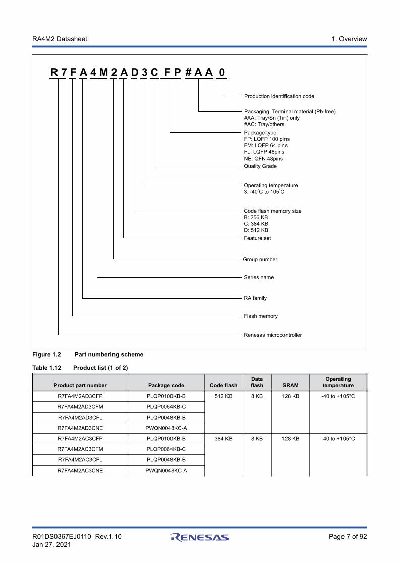
2.2.4 I/O VOH, VOL, and Other Characteristics
Table 2.6 I/O VOH, VOL, and other characteristics
Parameter Symbol Min Typ Max Unit Test conditions
Output voltage IIC VOL — — 0.4 V IOL = 3.0 mA
VOL — — 0.6 IOL = 6.0 mA
IIC*1 VOL — — 0.4 IOL = 15.0 mA (ICFER.FMPE = 1)
VOL — 0.4 — IOL = 20.0 mA (ICFER.FMPE = 1)
Ports P205, P206, P407 toP415, P708 (total 12 pins)*2
VOH VCC – 1.0 — — IOH = –20 mAVCC = 3.3 V
VOL — — 1.0 IOL = 20 mAVCC = 3.3 V
Other output pins VOH VCC – 0.5 — — IOH = –1.0 mA
VOL — — 0.5 IOL = 1.0 mA
Input leakage current RES |Iin| — — 5.0 µA Vin = 0 VVin = 5.5 V
Port P200 — — 1.0 Vin = 0 VVin = VCC
Three-state leakage current(off state)
5 V-tolerant ports |ITSI| — — 5.0 µA Vin = 0 VVin = 5.5 V
Other ports (except for portP200)
— — 1.0 Vin = 0 VVin = VCC
Input pull-up MOS current Ports P0 to P7 Ip –300 — –10 µA VCC = 2.7 to 3.6 VVin = 0 V
Input capacitance USB_DP, USB_DM, and portsP014, P015, P400, P401
Cin — — 16 pF Vbias = 0 VVamp = 20 mVf = 1 MHzTa = 25°COther input pins — — 8
Note 1. SCL0_A, SDA0_A (total 2 pins).Note 2. This is the value when high driving ability is selected in the Port Drive Capability bit in the PmnPFS register.
The selected driving ability is retained in Deep Software Standby mode.
RA4M2 Datasheet 2. Electrical Characteristics
R01DS0367EJ0110 Rev.1.10Jan 27, 2021
Page 23 of 92

2.2.5 Operating and Standby CurrentTable 2.7 Operating and standby current (1 of 2)
Parameter Symbol Min Typ Max Unit Test conditions
Supplycurrent*1
High-speedmode
Maximum*2 *13 ICC*3 — — 65 mA ICLK = 100MHzPCLKA = 100MHzPCLKB = 50MHzPCLKC = 50MHzPCLKD = 100MHzFCLK = 50 MHz
CoreMark®*5 *6 *12 *14 — 8.1 —
Normal mode All peripheral clocks enabled,while (1) code executing fromflash*4 *12
— 15.4 —
All peripheral clocks disabled,while (1) code executing fromflash*5 *6 *12 *14
— 6.1 —
Sleep mode*5 *14 — 4.4*6*12
25*7*13
Increaseduring BGOoperation
Data flash P/E — 6 —
Code flash P/E — 8 —
Low-speed mode*5 *10 — 0.8 — ICLK = 1 MHz
Subosc-speed mode*5 *11 — 0.7 — ICLK = 32.768kHz
Software Standby mode SNZCR.RXDREQEN = 1 — — 14 —
SNZCR.RXDREQEN = 0 — 0.7 — —
DeepSoftwareStandbymode
Power supplied to Standby SRAM and USBresume detecting unit
— 16 96 µA —
Power notsupplied toSRAM or USBresumedetecting unit
Power-on reset circuit low powerfunction disabled
— 12 27 —
Power-on reset circuit low powerfunction enabled
— 5 17 —
Increase whenthe RTC andAGT areoperating
When the low-speed on-chiposcillator (LOCO) is in use
— 4.4 — —
When a crystal oscillator for lowclock loads is in use
— 1.0 — —
When a crystal oscillator forstandard clock loads is in use
— 1.6 — —
RTC operating while VCC is off (with thebattery backup function, only the RTC andsub-clock oscillator operate)
When a crystaloscillator for lowclock loads is in use
— 0.6 — VBATT = 1.8 V,VCC = 0 V
— 1.2 — VBATT = 3.3 V,VCC = 0 V
When a crystaloscillator forstandard clockloads is in use
— 1.1 — VBATT = 1.8 V,VCC = 0 V
— 1.8 — VBATT = 3.3 V,VCC = 0 V
Inrush current on returning from deepsoftware standby mode
Inrush current*8 IRUSH — 160 — mA
Energy of inrushcurrent*8
ERUSH — 1.0 — µC
RA4M2 Datasheet 2. Electrical Characteristics
R01DS0367EJ0110 Rev.1.10Jan 27, 2021
Page 24 of 92
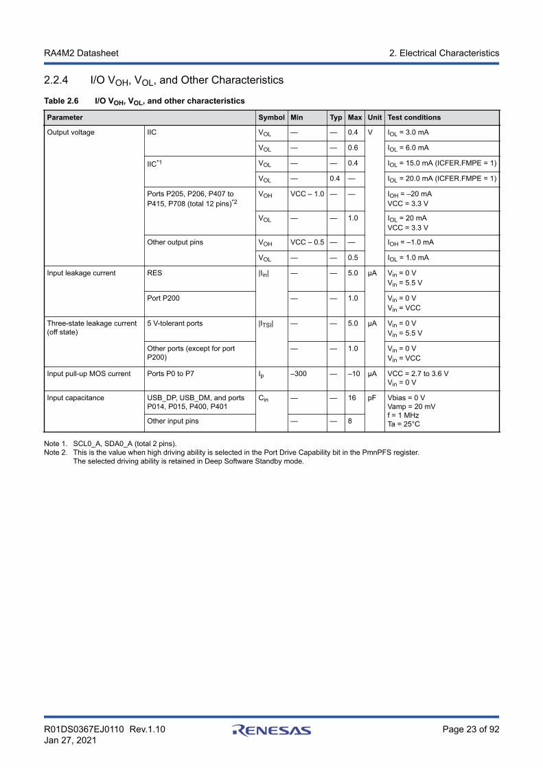
Table 2.7 Operating and standby current (2 of 2)
Parameter Symbol Min Typ Max Unit Test conditions
Analogpowersupplycurrent
During 12-bit A/D conversion AICC — 0.8 1.1 mA —
Temperature sensor — 0.1 0.2 mA —
During D/A conversion (per unit) Without AMP output — 0.1 0.2 mA —
With AMP output — 0.6 1.1 mA —
Waiting for A/D, D/A conversion (all units) — 0.5 1.0 mA —
ADC12, DAC12 in standby modes (all units)*9 — 0.4 4.0 µA —
Referencepowersupplycurrent(VREFH0)
During 12-bit A/D conversion (unit 0) AIREFH0 — 70 120 µA —
Waiting for 12-bit A/D conversion (unit 0) — 0.07 0.5 µA —
ADC12 in standby modes (unit 0) — 0.07 0.5 µA —
Referencepowersupplycurrent(VREFH)
During D/A conversion (per unit) Without AMP output AIREFH — 0.1 0.4 mA —
With AMP ouput — 0.1 0.4 mA —
Waiting for D/A (all units) conversion — 0.07 0.8 µA —
USBoperatingcurrent
Low speed USB ICCUSBLS — 3.5 6.5 mA VCC_USB
Full speed USB ICCUSBFS — 4.0 10.0 mA VCC_USB
LDOn operating current (1 unit)*15 ICCLDO — 0.18 — mA —
PLL2-LDO operating current ICCPLL2LDO — 0.21 — mA —
Note 1. Supply current values are with all output pins unloaded and all input pull-up MOSs in the off state.Note 2. Measured with clocks supplied to the peripheral functions. This does not include the BGO operation.Note 3. ICC depends on f (ICLK) as follows.
ICC Max. = 0.53 × f + 12 (max. operation in high-speed mode)ICC Typ. = 0.05 × f + 1.85 (normal operation in high-speed mode, all peripheral clocks disabled)ICC Typ. = 0.12 × f + 0.69 (low-speed mode)ICC Max. = 0.13 × f + 12 (sleep mode)
Note 4. This does not include the BGO operation.Note 5. Supply of the clock signal to peripherals is stopped in this state. This does not include the BGO operation.Note 6. FCLK, PCLKA, PCLKB, PCLKC, and PCLKD are set to divided by 64 (1.563 MHz).Note 7. FCLK, PCLKA, PCLKB, PCLKC, and PCLKD are set to divided by 64 (3.125 MHz).Note 8. Reference valueNote 9. When the MCU is in Software Standby mode or the MSTPCRD.MSTPD16 (12-Bit A/D Converter 0 Module Stop bit) is in the
module-stop state.Note 10. FCLK, PCLKA, PCLKB, PCLKC, and PCLKD are set to divided by 64 (15.6 kHz).Note 11. PCLKA, PCLKB, PCLKC, and PCLKD are set to divided by 64 (512 Hz). FCLK is the same frequency as that of ICLK.Note 12. PLL output frequency = 100MHz.Note 13. PLL output frequency = 200MHz.Note 14. PLL2-LDO disabled.Note 15. n = 0, 1
RA4M2 Datasheet 2. Electrical Characteristics
R01DS0367EJ0110 Rev.1.10Jan 27, 2021
Page 25 of 92

Table 2.8 Coremark and normal mode current
Parameter Symbol Typ Unit Test conditions
Supply Current*1 Coremark*2 *3 *4 ICC 81 µA/MHz ICLK = 100MHzPCLKA= PCLKB= PCLKC= PCLKD= FCLK= 1.56 MHz
Normal mode All peripheralclocks disabled,cache on, while(1) codeexecuting fromflash*2 *3 *4
60
All peripheralclocks disabled,cache off, while(1) codeexecuting fromflash*2 *3 *4
118
Note 1. Supply current values are with all output pins unloaded and all input pull-up MOSs in the off state.Note 2. Supply of the clock signal to peripherals is stopped in this state. This does not include the BGO operation.Note 3. PLL output frequency = 100MHz.Note 4. PLL2-LDO disabled.
Under development Preliminary document Specifications in this document are tentative and subject to change
RA4M2 Series 59. Electrical Characteristics
xx xx, 2019 RA4M2 Target Spec Page 9 of 2123
Figure 47.2 Temperature dependency in Software Standby mode (reference data)
Figure 47.3 Temperature dependency in Deep Software Standby mode, power supplied to standby SRAM and USB resume detecting unit (reference data)
1
10
100
1000
-40 -20 0 20 40 60 80 100
ICC
(u
A)
Ta ()
Average value of the tested middle samples during product evaluation.
Average value of the tested upper-limit samples during product evaluation.
0.1
1.0
10.0
100.0
-40 -20 0 20 40 60 80 100
ICC
(m
A)
Ta ()
Average value of the tested middle samples during product evaluation.
Average value of the tested upper-limit samples during product evaluation.
Figure 2.2 Temperature dependency in Software Standby mode (reference data)
RA4M2 Datasheet 2. Electrical Characteristics
R01DS0367EJ0110 Rev.1.10Jan 27, 2021
Page 26 of 92

Under development Preliminary document Specifications in this document are tentative and subject to change
RA4M2 Series 59. Electrical Characteristics
xx xx, 2019 RA4M2 Target Spec Page 9 of 2123
Figure 47.2 Temperature dependency in Software Standby mode (reference data)
Figure 47.3 Temperature dependency in Deep Software Standby mode, power supplied to standby SRAM and USB resume detecting unit (reference data)
1
10
100
1000
-40 -20 0 20 40 60 80 100
ICC
(u
A)
Ta ()
Average value of the tested middle samples during product evaluation.
Average value of the tested upper-limit samples during product evaluation.
0.1
1.0
10.0
100.0
-40 -20 0 20 40 60 80 100
ICC
(m
A)
Ta ()
Average value of the tested middle samples during product evaluation.
Average value of the tested upper-limit samples during product evaluation.
Figure 2.3 Temperature dependency in Deep Software Standby mode, power supplied to standby SRAMand USB resume detecting unit (reference data)Under development Preliminary document
Specifications in this document are tentative and subject to change
RA4M3 Series 59. Electrical Characteristics
xx xx, 2019 RA4M2 Starget Spec Page 10 of 2123
Figure 47.4 Temperature dependency in Deep Software Standby mode, power not supplied to SRAM or USB resume detecting unit, power-on reset circuit low power function disabled (reference data)
Figure 47.5 Temperature dependency in Deep Software Standby mode, power not supplied to SRAM or USB resume detecting unit, power-on reset circuit low power function enabled (reference data)
1
10
100
-40 -20 0 20 40 60 80 100
ICC
(u
A)
Ta ()
Average value of the tested middle samples during product evaluation.
Average value of the tested upper-limit samples during product evaluation.
1
10
100
-40 -20 0 20 40 60 80 100
ICC
(u
A)
Ta ()
Average value of the tested middle samples during product evaluation.
Average value of the tested upper-limit samples during product evaluation.
Figure 2.4 Temperature dependency in Deep Software Standby mode, power not supplied to SRAM orUSB resume detecting unit, power-on reset circuit low power function disabled (referencedata)
RA4M2 Datasheet 2. Electrical Characteristics
R01DS0367EJ0110 Rev.1.10Jan 27, 2021
Page 27 of 92

Under development Preliminary document Specifications in this document are tentative and subject to change
RA4M3 Series 59. Electrical Characteristics
xx xx, 2019 RA4M2 Starget Spec Page 10 of 2123
Figure 47.4 Temperature dependency in Deep Software Standby mode, power not supplied to SRAM or USB resume detecting unit, power-on reset circuit low power function disabled (reference data)
Figure 47.5 Temperature dependency in Deep Software Standby mode, power not supplied to SRAM or USB resume detecting unit, power-on reset circuit low power function enabled (reference data)
1
10
100
-40 -20 0 20 40 60 80 100
ICC
(u
A)
Ta ()
Average value of the tested middle samples during product evaluation.
Average value of the tested upper-limit samples during product evaluation.
1
10
100
-40 -20 0 20 40 60 80 100
ICC
(u
A)
Ta ()
Average value of the tested middle samples during product evaluation.
Average value of the tested upper-limit samples during product evaluation.
Figure 2.5 Temperature dependency in Deep Software Standby mode, power not supplied to SRAM orUSB resume detecting unit, power-on reset circuit low power function enabled (reference data)
2.2.6 VCC Rise and Fall Gradient and Ripple FrequencyTable 2.9 Rise and fall gradient characteristics
Parameter Symbol Min Typ Max UnitTestconditions
VCC rising gradient Voltage monitor 0 reset disabled at startup SrVCC 0.0084 — 20 ms/V —
Voltage monitor 0 reset enabled at startup 0.0084 — — —
SCI/USB boot mode*1 0.0084 — 20 —
VCC falling gradient*2 SfVCC 0.0084 — — ms/V —
Note 1. At boot mode, the reset from voltage monitor 0 is disabled regardless of the value of the OFS1.LVDAS bit.Note 2. This applies when VBATT is used.
Table 2.10 Rising and falling gradient and ripple frequency characteristics The ripple voltage must meet the allowable ripple frequency fr(VCC) within the range between the VCC upper limit (3.6 V) and lower limit (2.7V). When the VCC change exceeds VCC ±10%, the allowable voltage change rising and falling gradient dt/dVCC must be met.Parameter Symbol Min Typ Max Unit Test conditions
Allowable ripplefrequency
fr (VCC) — — 10 kHz Figure 2.6Vr (VCC) ≤ VCC × 0.2
— — 1 MHz Figure 2.6Vr (VCC) ≤ VCC × 0.08
— — 10 MHz Figure 2.6Vr (VCC) ≤ VCC × 0.06
Allowable voltagechange rising andfalling gradient
dt/dVCC 1.0 — — ms/V When VCC changeexceeds VCC ±10%
RA4M2 Datasheet 2. Electrical Characteristics
R01DS0367EJ0110 Rev.1.10Jan 27, 2021
Page 28 of 92

Vr(VCC)VCC
1 / fr(VCC)
Figure 2.6 Ripple waveform
2.2.7 Thermal Characteristics
Maximum value of junction temperature (Tj) must not exceed the value of “section 2.2.1. Tj/Ta Definition”.Tj is calculated by either of the following equations. Tj = Ta + θja × Total power consumption Tj = Tt + Ψjt × Total power consumption
– Tj : Junction Temperature (°C)– Ta : Ambient Temperature (°C)– Tt : Top Center Case Temperature (°C)– θja : Thermal Resistance of “Junction”-to-“Ambient” (°C/W)– Ψjt : Thermal Resistance of “Junction”-to-“Top Center Case” (°C/W)
Total power consumption = Voltage × (Leakage current + Dynamic current) Leakage current of IO = Σ (IOL × VOL) /Voltage + Σ (|IOH| × |VCC – VOH|) /Voltage
Dynamic current of IO = Σ IO (Cin + Cload) × IO switching frequency × Voltage
– Cin: Input capacitance
– Cload: Output capacitance
Regarding θja and Ψjt, refer to Table 2.11.
Table 2.11 Thermal Resistance
Parameter Package Symbol Value*1 Unit Test conditions
ThermalResistance
48-pin QFN (PWQN0048KC-A) θja 23.9 °C/W JESD 51-2 and 51-7compliant
48-pin LQFP (PLQP0048KB-B) 62.1
64-pin LQFP (PLQP0064KB-C) 54.6
100-pin LQFP (PLQP0100KB-B) 55.1
48-pin QFN (PWQN0048KC-A) Ψjt 0.28 °C/W JESD 51-2 and 51-7compliant
48-pin LQFP (PLQP0048KB-B) 2.39
64-pin LQFP (PLQP0064KB-C) 1.90
100-pin LQFP (PLQP0100KB-B) 1.90
Note 1. The values are reference values when the 4-layer board is used. Thermal resistance depends on the number of layers or size of theboard. For details, refer to the JEDEC standards.
2.2.7.1 Calculation guide of ICCmax
RA4M2 Datasheet 2. Electrical Characteristics
R01DS0367EJ0110 Rev.1.10Jan 27, 2021
Page 29 of 92
Table 2.12 shows the power consumption of each unit.
Table 2.12 Power consumption of each unit
Dynamic current/Leakage current
MCUDomain Category Item
Frequency[MHz]
Current[uA/MHz]
Current*1[mA]
Leakage current Analog LDO and Leak*2 Ta = 75 °C*3 — — 7.82
Ta = 85 °C*3 — — 9.13
Ta = 95 °C*3 — — 11.08
Ta = 105 °C*3 — — 14.33
Dynamic current CPU Operation withFlash and SRAM
Coremark 100 55.556 5.56
Peripheral Unit Timer GPT16 (4ch)*4 100 3.575 0.36
GPT32 (4ch)*4 100 4.230 0.42
POEG (4 Groups) 50 1.361 0.07
AGT (6ch)*4 50 9.228 0.46
RTC 50 4.277 0.21
WDT 50 0.764 0.04
IWDT 50 0.339 0.02
Communicationinterfaces
USBFS 50 9.385 0.47
SCI (6ch)*4 100 18.715 1.87
IIC (2ch)*4 50 3.367 0.16
CAN 50 1.898 0.09
SPI 100 3.024 0.30
QSPI 100 2.051 0.21
SSIE 50 3.208 0.16
SDHI 50 6.341 0.32
Analog ADC12 100 2.287 0.23
DAC12 (2ch)*4 100 0.869 0.09
TSN 50 0.166 0.01
Human machineinterfaces
CTSU 50 0.605 0.03
Event link ELC 50 0.865 0.04
Security SCE9 100 218.100 21.81
Data processing CRC 100 0.600 0.06
DOC 100 0.388 0.04
System CAC 50 0.844 0.04
DMA DMAC 100 4.479 0.45
DTC 100 4.274 0.43
Note 1. The values are guaranteed by design.Note 2. LDO and Leak are internal voltage regulator’s current and MCU’s leakage current.
It is selected according to the temperature of Ta.Note 3. Δ(Tj-Ta) = 20 °C is considered to measure the current.Note 4. To determine the current consumption per channel, group or unit, divide Current [mA] by the number of channels, groups or units.
Table 2.13 shows the outline of operation for each unit.
RA4M2 Datasheet 2. Electrical Characteristics
R01DS0367EJ0110 Rev.1.10Jan 27, 2021
Page 30 of 92

Table 2.13 Outline of operation for each unit
Peripheral Outline of operation
GPT Operating modes is set to saw-wave PWM mode.GPT is operating with PCLKD.
POEG Only clear module stop bit.
AGT AGT is operating with PCLKB.
RTC RTC is operating with LOCO.
WDT WDT is operating with PCLKB.
IWDT IWDT is operating with IWDTCLK.
USBFS Transfer types is set to bulk transfer.USBFS is operating using Full-speed transfer (12 Mbps).
SCI SCI is transmitting data in clock synchronous mode.
IIC Communication format is set to I2C-bus format.IIC is transmitting data in master mode.
CAN CAN is transmitting and receiving data in self-test mode 1.
SPI SPI mode is set to SPI operation (4-wire method).SPI master/slave mode is set to master mode.SPI is transmitting 8-bit width data.
QSPI QSPI is issuing Fast Read Quad I/O Instruction.
SSIE Communication mode is set to Master.System word length is set to 32 bits.Data word length is set to 20 bits.SSIE is transmitting data using I2S format.
SDHI Transfer bus mode is set to 4-bit wide bus mode.SDHI is issuing CMD24 (single-block write).
ADC12 Resolution is set to 12-bit accuracy.Data registers is set to A/D-converted value addition mode.ADC12 is converting the analog input in continuous scan mode.
DAC12 DAC12 is outputting the conversion result while updating the value of data register.
TSN TSN is operating.
CTSU CTSU is operating in self-capacitance single scan mode.
ELC Only clear module stop bit.
SCE9 SCE9 is executing built-in self test.
CRC CRC is generating CRC code using 32-bit CRC32-C polynomial.
DOC DOC is operating in data addition mode.
CAC Measurement target clocks is set to PCLKB.Measurement reference clocks is set to PCLKB.CAC is measuring the clock frequency accuracy.
DMAC Bit length of transfer data is set to 32 bits.Transfer mode is set to block transfer mode.DMAC is transferring data from SRAM0 to SRAM0.
DTC Bit length of transfer data is set to 32 bits.Transfer mode is set to block transfer mode.DTC is transferring data from SRAM0 to SRAM0.
2.2.7.2 Example of Tj calculation
Assumption : Package 100-pin LQFP : θja = 55.1 °C/W Ta = 100 °C ICCmax = 40 mA
RA4M2 Datasheet 2. Electrical Characteristics
R01DS0367EJ0110 Rev.1.10Jan 27, 2021
Page 31 of 92

VCC = 3.5 V (VCC = AVCC = VCC_USB) IOH = 1 mA, VOH = VCC – 0.5 V, 12 Outputs
IOL = 20 mA, VOL = 1.0 V, 8 Outputs
IOL = 1 mA, VOL = 0.5 V, 12 Outputs
Cin = 8 pF, 16 pins, Input frequency = 10 MHz
Cload = 30 pF, 16 pins, Output frequency = 10 MHz
Leakage current of IO = Σ (VOL × IOL) / Voltage + Σ ((VCC - VOH) × IOH) / Voltage
= (20 mA × 1 V) × 8 / 3.5 V + (1 mA × 0.5 V) × 12 / 3.5 V + ((VCC - (VCC - 0.5 V)) × 1 mA) × 12 / 3.5 V
= 45.7 mA + 1.71 mA + 1.71 mA
= 49.1 mA
Dynamic current of IO = Σ IO (Cin + Cload) × IO switching frequency × Voltage
= ((8 pF × 16) × 10 MHz + (30 pF × 16) × 10 MHz) × 3.5 V
= 21.3 mA
Total power consumption = Voltage × (Leakage current + Dynamic current)
= (40 mA × 3.5 V) + (49.1 mA + 21.3 mA) × 3.5 V
= 386 mW (0.386 W)
Tj = Ta + θja × Total power consumption
= 100 °C + 55.1 °C/W × 0.386W
= 121.3 °C
2.3 AC Characteristics
2.3.1 FrequencyTable 2.14 Operation frequency value in high-speed mode
Parameter Symbol Min Typ Max Unit
Operation frequency System clock (ICLK) f — — 100 MHz
Peripheral module clock (PCLKA) — — 100
Peripheral module clock (PCLKB) — — 50
Peripheral module clock (PCLKC) —*2 — 50
Peripheral module clock (PCLKD) — — 100
Flash interface clock (FCLK) —*1 — 50
Note 1. FCLK must run at a frequency of at least 4 MHz when programming or erasing the flash memory.Note 2. When the ADC12 is used, the PCLKC frequency must be at least 1 MHz.
RA4M2 Datasheet 2. Electrical Characteristics
R01DS0367EJ0110 Rev.1.10Jan 27, 2021
Page 32 of 92
Table 2.15 Operation frequency value in low-speed mode
Parameter Symbol Min Typ Max Unit
Operation frequency System clock (ICLK) f — — 1 MHz
Peripheral module clock (PCLKA) — — 1
Peripheral module clock (PCLKB) — — 1
Peripheral module clock (PCLKC) *2 —*2 — 1
Peripheral module clock (PCLKD) — — 1
Flash interface clock (FCLK)*1 — — 1
Note 1. Programming or erasing the flash memory is disabled in low-speed mode.Note 2. When the ADC12 is used, the PCLKC frequency must be set to at least 1 MHz.
Table 2.16 Operation frequency value in Subosc-speed mode
Parameter Symbol Min Typ Max Unit
Operation frequency System clock (ICLK) f 29.4 — 36.1 kHz
Peripheral module clock (PCLKA) — — 36.1
Peripheral module clock (PCLKB) — — 36.1
Peripheral module clock (PCLKC) *2 — — 36.1
Peripheral module clock (PCLKD) — — 36.1
Flash interface clock (FCLK)*1 29.4 — 36.1
Note 1. Programming or erasing the flash memory is disabled in Subosc-speed mode.Note 2. The ADC12 cannot be used.
2.3.2 Clock TimingTable 2.17 Clock timing except for sub-clock oscillator (1 of 2)
Parameter Symbol Min Typ Max Unit Test conditions
EXTAL external clock input cycle time tEXcyc 41.66 — — ns Figure 2.7
EXTAL external clock input high pulse width tEXH 15.83 — — ns
EXTAL external clock input low pulse width tEXL 15.83 — — ns
EXTAL external clock rise time tEXr — — 5.0 ns
EXTAL external clock fall time tEXf — — 5.0 ns
Main clock oscillator frequency fMAIN 8 — 24 MHz —
Main clock oscillation stabilization wait time (crystal)*1 tMAINOSCWT — — —*1 ms Figure 2.8
LOCO clock oscillation frequency fLOCO 29.4912 32.768 36.0448 kHz —
LOCO clock oscillation stabilization wait time tLOCOWT — — 60.4 µs Figure 2.9
ILOCO clock oscillation frequency fILOCO 13.5 15 16.5 kHz —
MOCO clock oscillation frequency FMOCO 6.8 8 9.2 MHz —
MOCO clock oscillation stabilization wait time tMOCOWT — — 15.0 µs —
RA4M2 Datasheet 2. Electrical Characteristics
R01DS0367EJ0110 Rev.1.10Jan 27, 2021
Page 33 of 92

Table 2.17 Clock timing except for sub-clock oscillator (2 of 2)
Parameter Symbol Min Typ Max Unit Test conditions
HOCO clock oscillator oscillationfrequency
Without FLL fHOCO16 15.78 16 16.22 MHz –20 ≤ Ta ≤ 105°C
fHOCO18 17.75 18 18.25
fHOCO20 19.72 20 20.28
fHOCO16 15.71 16 16.29 –40 ≤ Ta ≤ –20°C
fHOCO18 17.68 18 18.32
fHOCO20 19.64 20 20.36
With FLL fHOCO16 15.960 16 16.040 –40 ≤ Ta ≤ 105°CSub-clock frequency accuracyis ±50 ppm.fHOCO18 17.955 18 18.045
fHOCO20 19.950 20 20.050
HOCO clock oscillation stabilization wait time*2 tHOCOWT — — 64.7 µs —
HOCO period jitter — — ±85 — ps —
FLL stabilization wait time tFLLWT — — 1.8 ms —
PLL clock frequency fPLL 100 — 200 MHz —
PLL2 clock frequency fPLL2 120 — 240 MHz —
PLL/PLL2 clock oscillation stabilization wait time tPLLWT — — 174.9 µs Figure 2.10
PLL/PLL2 period jitter fPLL, fPLL2 ≥ 120MHz — — ±100 — ps —
fPLL, fPLL2 < 120MHz — — ±120 — ps —
PLL/PLL2 long term jitter — — ±300 — ps Term: 1µs, 10µs
Note 1. When setting up the main clock oscillator, ask the oscillator manufacturer for an oscillation evaluation, and use the results as therecommended oscillation stabilization time. Set the MOSCWTCR register to a value equal to or greater than the recommendedvalue.After changing the setting in the MOSCCR.MOSTP bit to start main clock operation, read the OSCSF.MOSCSF flag to confirm thatit is 1, and then start using the main clock oscillator.
Note 2. This is the time from release from reset state until the HOCO oscillation frequency (fHOCO) reaches the range for guaranteedoperation.
Table 2.18 Clock timing for the sub-clock oscillator
Parameter Symbol Min Typ Max Unit Test conditions
Sub-clock frequency fSUB — 32.768 — kHz —
Sub-clock oscillation stabilization wait time tSUBOSCWT — — —*1 s Figure 2.11
Note 1. When setting up the sub-clock oscillator, ask the oscillator manufacturer for an oscillation evaluation and use the results as therecommended oscillation stabilization time.After changing the setting in the SOSCCR.SOSTP bit to start sub-clock operation, only start using the sub-clock oscillator after thesub-clock oscillation stabilization time elapses with an adequate margin. A value that is two times the value shown is recommended.
RA4M2 Datasheet 2. Electrical Characteristics
R01DS0367EJ0110 Rev.1.10Jan 27, 2021
Page 34 of 92

tXH
tXcyc
EXTAL external clock input VCC × 0.5
tXL
tXr tXf
Figure 2.7 EXTAL external clock input timing
Main clock oscillator output
MOSCCR.MOSTP
Main clock
tMAINOSCWT
Figure 2.8 Main clock oscillation start timing
LOCO clock
LOCOCR.LCSTP
tLOCOWT
On-chip oscillator output
Figure 2.9 LOCO clock oscillation start timing
PLLCR.PLLSTPPLL2CR.PLL2STP
OSCSF.PLLSFOSCSF.PLL2SF
PLL/PLL2 clock
tPLLWT
PLL/PLL2 circuit output
Figure 2.10 PLL/PLL2 clock oscillation start timing
RA4M2 Datasheet 2. Electrical Characteristics
R01DS0367EJ0110 Rev.1.10Jan 27, 2021
Page 35 of 92

Sub-clock oscillator output
SOSCCR.SOSTP
Sub-clock
tSUBOSCWT
Figure 2.11 Sub-clock oscillation start timing
2.3.3 Reset TimingTable 2.19 Reset timing
Parameter Symbol Min Typ Max Unit Test conditions
RES pulse width Power-on tRESWP 0.7 — — ms Figure 2.12
Deep Software Standby mode tRESWD 0.6 — — ms Figure 2.13
Software Standby mode, Subosc-speedmode
tRESWS 0.3 — — ms
All other tRESW 200 — — µs
Wait time after RES cancellation tRESWT — 37.3 41.2 µs Figure 2.12
Wait time after internal reset cancellation(IWDT reset, WDT reset, software reset, SRAM parity error reset, SRAM ECC errorreset, bus master MPU error reset, TrustZone error reset)
tRESW2 — 324 397.7 µs —
VCC
RES
Internal reset signal(low is valid)
tRESWP
tRESWT
VCCmin
Figure 2.12 RES pin input timing under the condition that VCC exceeds VPOR voltage threshold
RES
Internal reset signal(low is valid)
tRESWD, tRESWS, tRESW
tRESWT
Figure 2.13 Reset input timing
RA4M2 Datasheet 2. Electrical Characteristics
R01DS0367EJ0110 Rev.1.10Jan 27, 2021
Page 36 of 92

2.3.4 Wakeup TimingTable 2.20 Timing of recovery from low power modes
Parameter Symbol Min Typ Max Unit Test conditions
Recovery time fromSoftware Standbymode*1
Crystal resonatorconnected to main clockoscillator
System clock source ismain clock oscillator*2
tSBYMC*13 — 2.1 2.4 ms Figure 2.14The division ratio of alloscillators is 1.
System clock source isPLL with main clockoscillator*3
tSBYPC*13 — 2.2 2.6 ms
External clock input tomain clock oscillator
System clock source ismain clock oscillator*4
tSBYEX*13 — 45 125 μs
System clock source isPLL with main clockoscillator*5
tSBYPE*13 — 170 255 μs
System clock source is sub-clock oscillator*6 *11 tSBYSC*13 — 0.7 0.8 ms
System clock source is LOCO*7 *11 tSBYLO*13 — 0.7 0.9 ms
System clock source is HOCO clock oscillator*8 tSBYHO*13 — 55 130 µs
System clock source is PLL with HOCO*9 tSBYPH*13 — 175 265 µs
System clock source is MOCO clock oscillator*10 tSBYMO*13 — 35 65 µs
Recovery time fromDeep SoftwareStandby mode
DPSBYCR.DEEPCUT[1] = 0 andDPSWCR.WTSTS[5:0] = 0x0E
tDSBY — 0.38 0.54 ms Figure 2.15
DPSBYCR.DEEPCUT[1] = 1 andDPSWCR.WTSTS[5:0] = 0x19
tDSBY — 0.55 0.73 ms
Wait time after cancellation of Deep Software Standby mode tDSBYWT 56 — 57 tcyc
Recovery time fromSoftware Standbymode to Snoozemode
High-speed mode when system clock source isHOCO (20 MHz)
tSNZ — 35*12 70*12 μs Figure 2.16
High-speed mode when system clock source isMOCO (8 MHz)
tSNZ — 11*12 14*12 μs
Note 1. The recovery time is determined by the system clock source. When multiple oscillators are active, the recovery time can bedetermined with the following equation:Total recovery time = recovery time for an oscillator as the system clock source + the longest tSBYOSCWT in the active oscillators -tSBYOSCWT for the system clock + 2 LOCO cycles (when LOCO is operating) + Subosc is oscillating and MSTPC0 = 0 (CACmodule stop))
Note 2. When the frequency of the crystal is 24 MHz (Main Clock Oscillator Wait Control Register (MOSCWTCR) is set to 0x05) and thegreatest value of the internal clock division setting is 1.
Note 3. When the frequency of PLL is 200 MHz (Main Clock Oscillator Wait Control Register (MOSCWTCR) is set to 0x05) and the greatestvalue of the internal clock division setting is 4.
Note 4. When the frequency of the external clock is 24 MHz (Main Clock Oscillator Wait Control Register (MOSCWTCR) is set to 0x00) andthe greatest value of the internal clock division setting is 1.
Note 5. When the frequency of PLL is 200 MHz (Main Clock Oscillator Wait Control Register (MOSCWTCR) is set to 0x00) and the greatestvalue of the internal clock division setting is 4.
Note 6. The Sub-clock oscillator frequency is 32.768 KHz and the greatest value of the internal clock division setting is 1.Note 7. The LOCO frequency is 32.768 KHz and the greatest value of the internal clock division setting is 1.Note 8. The HOCO frequency is 20 MHz and the greatest value of the internal clock division setting is 1.Note 9. The PLL frequency is 200 MHz and the greatest value of the internal clock division setting is 4.Note 10. The MOCO frequency is 8 MHz and the greatest value of the internal clock division setting is 1.Note 11. In Subosc-speed mode, the sub-clock oscillator or LOCO continues oscillating in Software Standby mode.Note 12. When the SNZCR.RXDREQEN bit is set to 0, the following time is added as the power supply recovery time: 16 µs (typical), 48 µs
(maximum).Note 13. The recovery time can be calcurated with the equation of tSBYOSCWT + tSBYSEQ. And they can be determined with the fol-lowing
value and equation. For n, the greatest value is selected from among the internal clock division settings.
Wakeup time TYP MAX Unit
tSBYOSCWT tSBYSEQ tSBYOSCWT tSBYSEQ
tSBYMC (MSTS[7:0]*32 + 3) /0.262
35 + 18 / fICLK + 4n / fMAIN (MSTS[7:0]*32 + 14 /0.236
62 + 18 / fICLK + 4n / fMAIN µs
RA4M2 Datasheet 2. Electrical Characteristics
R01DS0367EJ0110 Rev.1.10Jan 27, 2021
Page 37 of 92

Wakeup time TYP MAX Unit
tSBYOSCWT tSBYSEQ tSBYOSCWT tSBYSEQ
tSBYPC (MSTS[7:0]*32 + 34) /0.262
35 + 18 / fICLK + 4n / fPLL (MSTS[7:0]*32 + 45) /0.236
62 + 18 / fICLK + 4n / fPLL µs
tSBYEX 10 35 + 18 / fICLK + 4n / fEXMAIN 62 62 + 18 / fICLK + 4n / fEXMAIN µs
tSBYPE 135 35 + 18 / fICLK + 4n / fPLL 192 62 + 18 / fICLK + 4n / fPLL µs
tSBYSC 0 35 + 18 / fICLK + 4n / fSUB 0 62 + 18 / fICLK + 4n / fSUB µs
tSBYLO 0 35 + 18 / fICLK + 4n / fLOCO 0 62 + 18 / fICLK + 4n / fLOCO µs
tSBYHO 20 35 + 18 / fICLK + 4n / fHOCO 67 62 + 18 / fICLK + 4n / fHOCO µs
tSBYPH 140 35 + 18 / fICLK + 4n / fPLL 202 62 + 18 / fICLK + 4n / fPLL µs
tSBYMO 0 35 + 18 / fICLK + 4n / fMOCO 0 62 + 18 / fICLK + 4n / fMOCO µs
Oscillator(system clock)
ICLK
IRQSoftware Standby mode
tSBYMC, tSBYEX, tSBYPC, tSBYPE,
tSBYPH, tSBYSC, tSBYHO, tSBYLO
Oscillator(not the system clock)
tSBYOSCWT tSBYSEQ
Oscillator(system clock)
ICLK
IRQ
Software Standby mode
tSBYMC, tSBYEX, tSBYPC, tSBYPE,
tSBYPH, tSBYSC, tSBYHO, tSBYLO
tSBYOSCWT
tSBYOSCWT
When stabilization of the system clock oscillator is slower
tSBYSEQ
Oscillator(not the system clock)
When stabilization of an oscillator other than the system clock is slower
Figure 2.14 Software Standby mode cancellation timing
RA4M2 Datasheet 2. Electrical Characteristics
R01DS0367EJ0110 Rev.1.10Jan 27, 2021
Page 38 of 92

Oscillator
IRQ
Internal reset(low is valid)
Reset exception handling start
Deep Software Standby mode
Deep Software Standby reset
(low is valid)
tDSBY
tDSBYWT
Figure 2.15 Deep Software Standby mode cancellation timing
tSNZ
IRQ
ICLK (to DTC, SRAM)*1 PCLK
ICLK (except DTC, SRAM)
Oscillator
Software Standby mode Snooze mode
Note 1. When SNZCR.SNZDTCEN bit is set to 1, ICLK is supplied to DTC and SRAM.
Figure 2.16 Recovery timing from Software Standby mode to Snooze mode
2.3.5 NMI and IRQ Noise FilterTable 2.21 NMI and IRQ noise filter
Parameter Symbol Min Typ Max Unit Test conditions
NMI pulsewidth
tNMIW 200 — — ns NMI digital filterdisabled
tPcyc × 2 ≤ 200 ns
tPcyc × 2*1 — — tPcyc × 2 > 200 ns
200 — — NMI digital filterenabled
tNMICK × 3 ≤ 200 ns
tNMICK × 3.5*2 — — tNMICK × 3 > 200 ns
IRQ pulsewidth
tIRQW 200 — — ns IRQ digital filterdisabled
tPcyc × 2 ≤ 200 ns
tPcyc × 2*1 — — tPcyc × 2 > 200 ns
200 — — IRQ digital filterenabled
tIRQCK × 3 ≤ 200 ns
tIRQCK × 3.5*3 — — tIRQCK × 3 > 200 ns
RA4M2 Datasheet 2. Electrical Characteristics
R01DS0367EJ0110 Rev.1.10Jan 27, 2021
Page 39 of 92

Note: 200 ns minimum in Software Standby mode.Note: If the clock source is switched, add 4 clock cycles of the switched source.Note 1. tPcyc indicates the PCLKB cycle.Note 2. tNMICK indicates the cycle of the NMI digital filter sampling clock.Note 3. tIRQCK indicates the cycle of the IRQi digital filter sampling clock.
tNMIW
NMI
Figure 2.17 NMI interrupt input timing
tIRQW
IRQ
Figure 2.18 IRQ interrupt input timing
2.3.6 I/O Ports, POEG, GPT, AGT, and ADC12 Trigger TimingTable 2.22 I/O ports, POEG, GPT, AGT, and ADC12 trigger timing GPT32 Conditions:High drive output is selected in the Port Drive Capability bit in the PmnPFS register.AGT Conditions:Middle drive output is selected in the Port Drive Capability bit in the PmnPFS register.Parameter Symbol Min Max Unit Test conditions
I/O ports Input data pulse width tPRW 1.5 — tPcyc Figure 2.19
POEG POEG input trigger pulse width tPOEW 3 — tPcyc Figure 2.20
GPT Input capture pulse width Single edge tGTICW 1.5 — tPDcyc Figure 2.21
Dual edge 2.5 —
GTIOCxY output skew(x = 0 to 3, Y = A or B)
Middle drive buffer tGTISK*1 — 4 ns Figure 2.22
High drive buffer — 4
GTIOCxY output skew(x = 4 to 7, Y = A or B)
Middle drive buffer — 4
High drive buffer — 4
GTIOCxY output skew(x = 0 to 7, Y = A or B)
Middle drive buffer — 6
High drive buffer — 6
OPS output skewGTOUUP, GTOULO, GTOVUP,GTOVLO, GTOWUP, GTOWLO
tGTOSK — 5 ns Figure 2.23
AGT AGTIO, AGTEE input cycle tACYC*2 100 — ns Figure 2.24
AGTIO, AGTEE input high width, low width tACKWH, tACKWL 40 — ns
AGTIO, AGTO, AGTOA, AGTOB output cycle tACYC2 62.5 — ns
ADC12 ADC12 trigger input pulse width tTRGW 1.5 — tPcyc Figure 2.25
Note: tPcyc: PCLKB cycle, tPDcyc: PCLKD cycle.Note 1. This skew applies when the same driver I/O is used. If the I/O of the middle and high drivers is mixed, operation is not guaranteed.Note 2. Constraints on input cycle:
RA4M2 Datasheet 2. Electrical Characteristics
R01DS0367EJ0110 Rev.1.10Jan 27, 2021
Page 40 of 92

When not switching the source clock: tPcyc × 2 < tACYC should be satisfied.When switching the source clock: tPcyc × 6 < tACYC should be satisfied.
Port
tPRW
Figure 2.19 I/O ports input timing
POEG input trigger
tPOEW
Figure 2.20 POEG input trigger timing
Input capture
tGTICW
Figure 2.21 GPT input capture timing
GPT output
PCLKD
tGTISK
Output delay
Figure 2.22 GPT output delay skew
RA4M2 Datasheet 2. Electrical Characteristics
R01DS0367EJ0110 Rev.1.10Jan 27, 2021
Page 41 of 92

GPT output
PCLKD
tGTOSK
Output delay
Figure 2.23 GPT output delay skew for OPS
tACYC2
AGTIO, AGTEE(input)
tACYC
tACKWL tACKWH
AGTIO, AGTO,AGTOA, AGTOB(output)
Figure 2.24 AGT input/output timing
ADTRG0
tTRGW
Figure 2.25 ADC12 trigger input timing
2.3.7 CAC TimingTable 2.23 CAC timing
Parameter Symbol Min Typ Max Unit Test conditions
CAC CACREF input pulsewidth
tPBcyc ≤ tcac*1 tCACREF 4.5 × tcac + 3 × tPBcyc — — ns —
tPBcyc > tcac*1 5 × tcac + 6.5 × tPBcyc — — ns
RA4M2 Datasheet 2. Electrical Characteristics
R01DS0367EJ0110 Rev.1.10Jan 27, 2021
Page 42 of 92

Note: tPBcyc: PCLKB cycle.Note 1. tcac: CAC count clock source cycle.
2.3.8 SCI TimingTable 2.24 SCI timing (1) Conditions: High drive output is selected in the Port Drive Capability bit in the PmnPFS register.Parameter Symbol Min Max Unit Test conditions
SCI Input clock cycle Asynchronous tScyc 4 — tPcyc Figure 2.26
Clock synchronous 6 —
Input clock pulse width tSCKW 0.4 0.6 tScyc
Input clock rise time tSCKr — 5 ns
Input clock fall time tSCKf — 5 ns
Output clock cycle Asynchronous tScyc 6 (other than SCI1,SCI2)8 (SCI1, SCI2)
— tPcyc
Clock synchronous 4 —
Output clock pulse width tSCKW 0.4 0.6 tScyc
Output clock rise time tSCKr — 5 ns
Output clock fall time tSCKf — 5 ns
Transmit data delay Clock synchronous master mode (internalclock)
tTXD — 5 ns Figure 2.27
Clock synchronous slave mode (externalclock)
tTXD — 25 ns
Receive data setup time Clock synchronous master mode (internalclock)
tRXS 15 — ns
Clock synchronous slave mode (externalclock)
tRXS 5 — ns
Receive data hold time Clock synchronous tRXH 5 — ns
Note: tPcyc: PCLKA cycle.
tSCKW tSCKr tSCKf
tScyc
SCKn
Note: n = 0 to 4, 9
Figure 2.26 SCK clock input/output timing
RA4M2 Datasheet 2. Electrical Characteristics
R01DS0367EJ0110 Rev.1.10Jan 27, 2021
Page 43 of 92
tTXD
tRXS tRXH
TXDn
RXDn
SCKn
Note: n = 0 to 4, 9
Figure 2.27 SCI input/output timing in clock synchronous mode
Table 2.25 SCI timing (2) Conditions: High drive output is selected in the Port Drive Capability bit in the PmnPFS register.Parameter Symbol Min Max Unit Test conditions
Simple SPI SCK clock cycle output (master) tSPcyc 4 65536 tPcyc Figure 2.28
SCK clock cycle input (slave) 6 65536
SCK clock high pulse width tSPCKWH 0.4 0.6 tSPcyc
SCK clock low pulse width tSPCKWL 0.4 0.6 tSPcyc
SCK clock rise and fall time tSPCKr, tSPCKf — 5 ns
Data input setup time master tSU 15 — ns Figure 2.29 to Figure2.32
slave 5 — ns
Data input hold time tH 5 — ns
SS input setup time tLEAD 1 — tSPcyc
SS input hold time tLAG 1 — tSPcyc
Data output delay master tOD — 5 ns
slave — 25 ns
Data output hold time tOH -5 — ns
Data rise and fall time tDr, tDf — 5 ns
SS input rise and fall time tSSLr, tSSLf — 5 ns
Slave access time tSA — 3 × tPcyc + 25 ns Figure 2.32
Slave output release time tREL — 3 × tPcyc + 25 ns
Note: tPcyc: PCLKA cycle.
RA4M2 Datasheet 2. Electrical Characteristics
R01DS0367EJ0110 Rev.1.10Jan 27, 2021
Page 44 of 92

tSPCKWH
VOH VOH
VOL VOL
VOH VOH
tSPCKWL
tSPCKr tSPCKf
VOL
tSPcyc
tSPCKWH
VIH VIH
VIL VIL
VIH VIH
tSPCKWL
tSPCKr tSPCKf
VIL
tSPcyc
VOH = 0.7 × VCC, VOL = 0.3 × VCC, VIH = 0.7 × VCC, VIL = 0.3 × VCC
SCKnmaster select output
SCKnslave select input
Note: n = 0 to 4, 9
Figure 2.28 SCI simple SPI mode clock timing
tDr, tDf
tSU tH
tOH tOD
MSB IN DATA LSB IN MSB IN
MSB OUT DATA LSB OUT IDLE MSB OUT
SCKnCKPOL = 0output
SCKnCKPOL = 1output
MISOninput
MOSInoutput
Note: n = 0 to 4, 9
Figure 2.29 SCI simple SPI mode timing for master when CKPH = 1
RA4M2 Datasheet 2. Electrical Characteristics
R01DS0367EJ0110 Rev.1.10Jan 27, 2021
Page 45 of 92

tSU tH
tOH tOD
MSB IN DATA LSB IN MSB IN
MSB OUT DATA LSB OUT IDLE MSB OUT
SCKnCKPOL = 1output
SCKnCKPOL = 0output
MISOninput
MOSInoutput
tDr, tDf
Note: n = 0 to 4, 9
Figure 2.30 SCI simple SPI mode timing for master when CKPH = 0
tDr, tDftSU tH
tLEAD
tTD
tLAG
tSA
MSB IN DATA LSB IN MSB IN
MSB OUT DATA LSB OUT MSB IN MSB OUT
tOH tOD tREL
SSninput
SCKnCKPOL = 0input
SCKnCKPOL = 1input
MISOnoutput
MOSIninput
Note: n = 0 to 4, 9
Figure 2.31 SCI simple SPI mode timing for slave when CKPH = 1
RA4M2 Datasheet 2. Electrical Characteristics
R01DS0367EJ0110 Rev.1.10Jan 27, 2021
Page 46 of 92

tDr, tDf
tSA tOH
tLEAD
tTD
tLAG
tH
LSB OUT(Last data) DATA MSB OUT
MSB IN DATA LSB IN MSB IN
LSB OUT
tSU
tOD tREL
MSB OUT
SSninput
SCKnCKPOL = 1input
SCKnCKPOL = 0input
MISOnoutput
MOSIninput
Note: n = 0 to 4, 9
Figure 2.32 SCI simple SPI mode timing for slave when CKPH = 0
Table 2.26 SCI timing (3) Conditions: Middle drive output is selected in the Port Drive Capability bit in the PmnPFS register.Parameter Symbol Min Max Unit Test conditions
Simple IIC(Standard mode)
SDA input rise time tSr — 1000 ns Figure 2.33
SDA input fall time tSf — 300 ns
SDA input spike pulse removal time tSP 0 4 × tIICcyc ns
Data input setup time tSDAS 250 — ns
Data input hold time tSDAH 0 — ns
SCL, SDA capacitive load Cb*1 — 400 pF
Simple IIC(Fast mode)
SDA input rise time tSr — 300 ns Figure 2.33
SDA input fall time tSf — 300 ns
SDA input spike pulse removal time tSP 0 4 × tIICcyc ns
Data input setup time tSDAS 100 — ns
Data input hold time tSDAH 0 — ns
SCL, SDA capacitive load Cb*1 — 400 pF
Note: tIICcyc: IIC internal reference clock (IICφ) cycle.Note 1. Cb indicates the total capacity of the bus line.
RA4M2 Datasheet 2. Electrical Characteristics
R01DS0367EJ0110 Rev.1.10Jan 27, 2021
Page 47 of 92

SDAn
SCLn
VIH
VIL
P*1 S*1
tSftSr
tSDAH tSDAS
tSP
P*1
Test conditions:VIH = VCC × 0.7, VIL = VCC × 0.3VOL = 0.6 V, IOL = 6 mA
Sr*1
Note: n = 0 to 4, 9Note 1. S, P, and Sr indicate the following conditions:
S: Start conditionP: Stop conditionSr: Restart condition
Figure 2.33 SCI simple IIC mode timing
RA4M2 Datasheet 2. Electrical Characteristics
R01DS0367EJ0110 Rev.1.10Jan 27, 2021
Page 48 of 92

2.3.9 SPI TimingTable 2.27 SPI timing Conditions: High drive output is selected in the Port Drive Capability bit in the PmnPFS register.Parameter Symbol Min Max Unit Test conditions
SPI RSPCK clock cycle Master tSPcyc 2 4096 tPcyc Figure 2.34
Slave 4 4096
RSPCK clock highpulse width
Master tSPCKWH (tSPcyc – tSPCKr – tSPCKf) /2 – 3
— ns
Slave 0.4 0.6 tSPcyc
RSPCK clock lowpulse width
Master tSPCKWL (tSPcyc – tSPCKr – tSPCKf) /2 – 3
— ns
Slave 0.4 0.6 tSPcyc
RSPCK clock rise andfall time
Master tSPCKr, tSPCKf — 5 ns
Slave — 1 µs
Data input setup time Master tSU 4 — ns Figure 2.35 to Figure2.40
Slave 5 —
Data input hold time Master(PCLKAdivision ratioset to 1/2)
tHF 0 — ns
Master(PCLKAdivision ratioset to a valueother than1/2)
tH tPcyc —
Slave tH 20 —
SSL setup time Master tLEAD N × tSPcyc - 10*1 N × tSPcyc +100*1
ns
Slave 4 × tPcyc — ns
SSL hold time Master tLAG N × tSPcyc - 10*2 N × tSPcyc +100*2
ns
Slave 4 × tPcyc — ns
Data output delay Master tOD1 — 6.3 ns
tOD2 — 6.3
Slave tOD — 20
Data output hold time Master tOH 0 — ns
Slave 0 —
Successivetransmission delay
Master tTD tSPcyc + 2 × tPcyc 8 × tSPcyc + 2× tPcyc
ns
Slave 4 × tPcyc
MOSI and MISO riseand fall time
Output tDr, tDf — 5 ns
Input — 1 µs
SSL rise and fall time Output tSSLr, tSSLf — 5 ns
Input — 1 µs
Slave access time tSA — 25 ns Figure 2.39 andFigure 2.40
Slave output release time tREL — 25
RA4M2 Datasheet 2. Electrical Characteristics
R01DS0367EJ0110 Rev.1.10Jan 27, 2021
Page 49 of 92
Note: tPcyc: PCLKA cycle.Note: Must use pins that have a letter appended to their name, for instance “_A”, “_B”, to indicate group membership. For the SPI
interface, the AC portion of the electrical characteristics is measured for each group.Note 1. N is set to an integer from 1 to 8 by the SPCKD register.Note 2. N is set to an integer from 1 to 8 by the SSLND register.
RSPCKnmaster select output
RSPCKnslave select input
tSPCKWH
VOH VOH
VOL VOL
VOH VOH
tSPCKWL
tSPCKr tSPCKf
VOL
tSPcyc
tSPCKWH
VIH VIH
VIL VIL
VIH VIH
tSPCKWL
tSPCKr tSPCKf
VIL
tSPcyc
VOH = 0.7 × VCC, VOL = 0.3 × VCC, VIH = 0.7 × VCC, VIL = 0.3 × VCC
Note: n = A
Figure 2.34 SPI clock timing
tDr, tDf
tSU tH
tLEAD
tTD
tLAG
tSSLr, tSSLf
tOH tOD2
MSB IN DATA LSB IN MSB IN
MSB OUT DATA LSB OUT IDLE MSB OUT
SSLn0 to SSLn3output
RSPCKnCPOL = 0output
RSPCKnCPOL = 1output
MISOninput
MOSInoutput
SPI
tOD1
Note: n = A
Figure 2.35 SPI timing for master when CPHA = 0
RA4M2 Datasheet 2. Electrical Characteristics
R01DS0367EJ0110 Rev.1.10Jan 27, 2021
Page 50 of 92
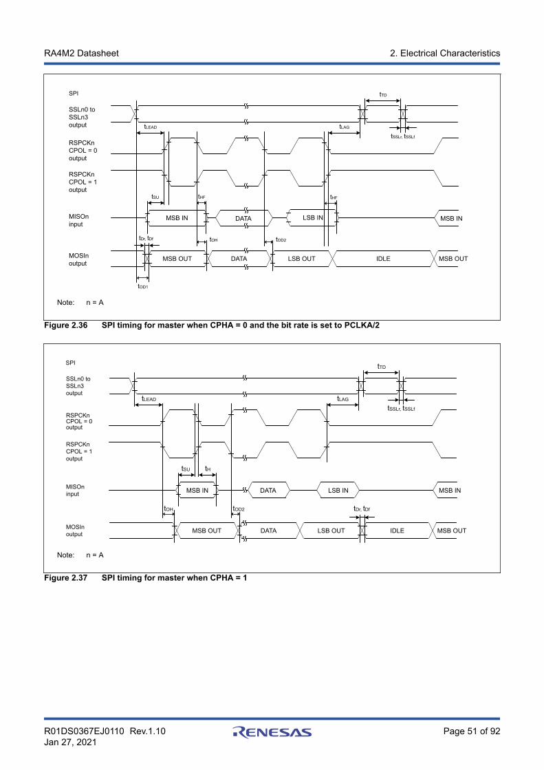
SSLn0 to SSLn3output
RSPCKnCPOL = 0output
RSPCKnCPOL = 1output
MISOninput
MOSInoutput
LSB IN
tDr, tDf
tSU tHF
tLEAD
tTD
tLAG
tSSLr, tSSLf
tOH tOD2
MSB IN
MSB OUT DATA LSB OUT IDLE MSB OUT
MSB IN DATA
tHF
SPI
tOD1
Note: n = A
Figure 2.36 SPI timing for master when CPHA = 0 and the bit rate is set to PCLKA/2
tSU tH
tLEAD
tTD
tLAG
tSSLr, tSSLf
tOH tOD2
MSB IN DATA LSB IN MSB IN
MSB OUT DATA LSB OUT IDLE MSB OUT
SSLn0 to SSLn3output
RSPCKnCPOL = 0output
RSPCKnCPOL = 1output
MISOninput
MOSInoutput
SPI
tDr, tDf
Note: n = A
Figure 2.37 SPI timing for master when CPHA = 1
RA4M2 Datasheet 2. Electrical Characteristics
R01DS0367EJ0110 Rev.1.10Jan 27, 2021
Page 51 of 92

tSU tHF
tLEAD
tTD
tLAG
tSSLr, tSSLf
tOH tOD2
MSB IN DATA LSB IN MSB IN
MSB OUT DATA LSB OUT IDLE MSB OUT
SSLn0 to SSLn3output
RSPCKnCPOL = 0output
RSPCKnCPOL = 1output
MISOninput
MOSInoutput
SPI
tDr, tDf
tH
Note: n = A
Figure 2.38 RSPI timing for master when CPHA = 1 and the bit rate is set to PCLKA/2
tDr, tDftSU tH
tLEAD
tTD
tLAG
tSA
MSB IN DATA LSB IN MSB IN
MSB OUT DATA LSB OUT MSB IN MSB OUT
tOH tOD tREL
SSLn0input
RSPCKnCPOL = 0input
RSPCKnCPOL = 1input
MISOnoutput
MOSIninput
Note: n = A
Figure 2.39 SPI timing for slave when CPHA = 0
RA4M2 Datasheet 2. Electrical Characteristics
R01DS0367EJ0110 Rev.1.10Jan 27, 2021
Page 52 of 92

SSLn0input
RSPCKnCPOL = 0input
RSPCKnCPOL = 1input
MISOnoutput
MOSIninput
tDr, tDf
tSA tOH
tLEAD
tTD
tLAG
tH
LSB OUT(Last data) DATA MSB OUT
MSB IN DATA LSB IN MSB IN
LSB OUT
tSU
tOD tREL
MSB OUT
Note: n = A
Figure 2.40 SPI timing for slave when CPHA = 1
2.3.10 QSPI Timing
Table 2.28 QSPI timing Conditions: High drive output is selected in the Port Drive Capability bit in the PmnPFS register.Parameter Symbol Min Max Unit Test conditions
QSPI QSPCK clock cycle tQScyc 2 48 tPcyc Figure 2.41
QSPCK clock high pulsewidth
tQSWH tQScyc × 0.4 — ns
QSPCK clock low pulsewidth
tQSWL tQScyc × 0.4 — ns
Data input setup time tSu 10 — ns Figure 2.42
Data input hold time tIH 0 — ns
QSSL setup time tLEAD (N + 0.5) × tQscyc - 5*1 (N + 0.5) × tQscyc +100*1
ns
QSSL hold time tLAG (N + 0.5) × tQscyc - 5*2 (N + 0.5) × tQscyc +100*2
ns
Data output delay tOD — 4 ns
Data output hold time tOH –3.3 — ns
Successive transmissiondelay
tTD 1 16 tQScyc
Note: tPcyc: PCLKA cycle.Note 1. N is set to 0 or 1 in SFMSLD.Note 2. N is set to 0 or 1 in SFMSHD.
RA4M2 Datasheet 2. Electrical Characteristics
R01DS0367EJ0110 Rev.1.10Jan 27, 2021
Page 53 of 92

tQScyc
QSPCLK output
tQSWH tQSWL
Figure 2.41 QSPI clock timing
tSU tH
tLEAD
tTD
tLAG
tOH tOD
MSB IN DATA LSB IN
MSB OUT DATA LSB OUT IDLE
QSSLoutput
QSPCLKoutput
QIO0-3input
QIO0-3output
Figure 2.42 Transmit and receive timing
RA4M2 Datasheet 2. Electrical Characteristics
R01DS0367EJ0110 Rev.1.10Jan 27, 2021
Page 54 of 92

2.3.11 IIC TimingTable 2.29 IIC timing (1) (1 of 2)(1) Conditions: Middle drive output is selected in the Port Drive Capability bit in the PmnPFS register for the following pins: SDA0_B,SCL0_B, SDA1_B, SCL1_B.(2) The following pins do not require setting: SCL0_A, SDA0_A.(3) Use pins that have a letter appended to their names, for instance “_A” or “_B”, to indicate group membership. For the IIC interface, theAC portion of the electrical characteristics is measured for each group.
Parameter Symbol Min Max UnitTestconditions
IIC(Standard mode,SMBus)ICFER.FMPE = 0
SCL input cycle time tSCL 6 (12) × tIICcyc + 1300 — ns Figure 2.43
SCL input high pulse width tSCLH 3 (6) × tIICcyc + 300 — ns
SCL input low pulse width tSCLL 3 (6) × tIICcyc + 300 — ns
SCL, SDA rise time tSr — 1000 ns
SCL, SDA fall time tSf — 300 ns
SCL, SDA input spike pulseremoval time
tSP 0 1 (4) × tIICcyc ns
SDA input bus free time whenwakeup function is disabled
tBUF 3 (6) × tIICcyc + 300 — ns
SDA input bus free time whenwakeup function is enabled
tBUF 3 (6) × tIICcyc + 4 × tPcyc +300
— ns
START condition input hold timewhen wakeup function is disabled
tSTAH tIICcyc + 300 — ns
START condition input hold timewhen wakeup function is enabled
tSTAH 1 (5) × tIICcyc + tPcyc + 300 — ns
Repeated START condition inputsetup time
tSTAS 1000 — ns
STOP condition input setup time tSTOS 1000 — ns
Data input setup time tSDAS tIICcyc + 50 — ns
Data input hold time tSDAH 0 — ns
SCL, SDA capacitive load Cb*2 — 400 pF
RA4M2 Datasheet 2. Electrical Characteristics
R01DS0367EJ0110 Rev.1.10Jan 27, 2021
Page 55 of 92

Table 2.29 IIC timing (1) (2 of 2)(1) Conditions: Middle drive output is selected in the Port Drive Capability bit in the PmnPFS register for the following pins: SDA0_B,SCL0_B, SDA1_B, SCL1_B.(2) The following pins do not require setting: SCL0_A, SDA0_A.(3) Use pins that have a letter appended to their names, for instance “_A” or “_B”, to indicate group membership. For the IIC interface, theAC portion of the electrical characteristics is measured for each group.
Parameter Symbol Min Max UnitTestconditions
IIC(Fast mode)
SCL input cycle time tSCL 6 (12) × tIICcyc + 600 — ns Figure 2.43
SCL input high pulse width tSCLH 3 (6) × tIICcyc + 300 — ns
SCL input low pulse width tSCLL 3 (6) × tIICcyc + 300 — ns
SCL, SDA rise time tSr 20 × (external pullupvoltage/5.5V)*1
300 ns
SCL, SDA fall time tSf 20 × (external pullupvoltage/5.5V)*1
300 ns
SCL, SDA input spike pulseremoval time
tSP 0 1 (4) × tIICcyc ns
SDA input bus free time whenwakeup function is disabled
tBUF 3 (6) × tIICcyc + 300 — ns
SDA input bus free time whenwakeup function is enabled
tBUF 3 (6) × tIICcyc + 4 × tPcyc +300
— ns
START condition input hold timewhen wakeup function is disabled
tSTAH tIICcyc + 300 — ns
START condition input hold timewhen wakeup function is enabled
tSTAH 1 (5) × tIICcyc + tPcyc + 300 — ns
Repeated START condition inputsetup time
tSTAS 300 — ns
STOP condition input setup time tSTOS 300 — ns
Data input setup time tSDAS tIICcyc + 50 — ns
Data input hold time tSDAH 0 — ns
SCL, SDA capacitive load Cb*2 — 400 pF
Note: tIICcyc: IIC internal reference clock (IICφ) cycle, tPcyc: PCLKB cycle.Note: Values in parentheses apply when ICMR3.NF[1:0] is set to 11b while the digital filter is enabled with ICFER.NFE set to 1.Note: Must use pins that have a letter appended to their name, for instance “_A”, “_B”, to indicate group membership. For the IIC
interface, the AC portion of the electrical characteristics is measured for each group.Note 1. Only supported for SCL0_A and SDA0_A.Note 2. Cb indicates the total capacity of the bus line.
RA4M2 Datasheet 2. Electrical Characteristics
R01DS0367EJ0110 Rev.1.10Jan 27, 2021
Page 56 of 92

Table 2.30 IIC timing (2) Setting of the SCL0_A, SDA0_A pins is not required with the Port Drive Capability bit in the PmnPFS register.Parameter Symbol Min Max Unit Test conditions
IIC(Fast-mode+)ICFER.FMPE = 1
SCL input cycle time tSCL 6 (12) × tIICcyc +240
— ns Figure 2.43
SCL input high pulse width tSCLH 3 (6) × tIICcyc + 120 — ns
SCL input low pulse width tSCLL 3 (6) × tIICcyc + 120 — ns
SCL, SDA rise time tSr — 120 ns
SCL, SDA fall time tSf 20 × (externalpullup voltage/5.5V)
120 ns
SCL, SDA input spike pulseremoval time
tSP 0 1 (4) × tIICcyc ns
SDA input bus free time whenwakeup function is disabled
tBUF 3 (6) × tIICcyc + 120 — ns
SDA input bus free time whenwakeup function is enabled
tBUF 3 (6) × tIICcyc + 4 ×tPcyc + 120
— ns
Start condition input hold timewhen wakeup function is disabled
tSTAH tIICcyc + 120 — ns
START condition input hold timewhen wakeup function is enabled
tSTAH 1 (5) × tIICcyc +tPcyc + 120
— ns
Restart condition input setup time tSTAS 120 — ns
Stop condition input setup time tSTOS 120 — ns
Data input setup time tSDAS tIICcyc + 30 — ns
Data input hold time tSDAH 0 — ns
SCL, SDA capacitive load Cb*1 — 550 pF
Note: tIICcyc: IIC internal reference clock (IICφ) cycle, tPcyc: PCLKB cycle.Note: Values in parentheses apply when ICMR3.NF[1:0] is set to 11b while the digital filter is enabled with ICFER.NFE set to 1.Note 1. Cb indicates the total capacity of the bus line.
RA4M2 Datasheet 2. Electrical Characteristics
R01DS0367EJ0110 Rev.1.10Jan 27, 2021
Page 57 of 92

SDAn
SCLn
VIH
VIL
tSTAHtSCLH
tSCLL
P*1 S*1
tSf tSr
tSCLtSDAH
tSDAS
tSTAS tSP tSTOS
P*1
tBUF
Sr*1
Note 1. S, P, and Sr indicate the following conditions:S: Start conditionP: Stop conditionSr: Restart condition
Figure 2.43 I2C bus interface input/output timing
2.3.12 SSIE Timing
Table 2.31 SSIE timing (1) High drive output is selected with the Port Drive Capability bit in the PmnPFS register.(2) Use pins that have a letter appended to their names, for instance “_A” or “_B” to indicate group membership. For the SSIE interface, theAC portion of the electrical characteristics is measured for each group.
Parameter Symbol
Target specification
Unit CommentsMin. Max.
SSIBCK0 Cycle Master tO 80 — ns Figure 2.44
Slave tI 80 — ns
High level/ lowlevel
Master tHC/tLC 0.35 — tO
Slave 0.35 — tI
Rising time/falling time
Master tRC/tFC — 0.15 tO / tI
Slave — 0.15 tO / tI
SSILRCK0/SSIFS0,SSITXD0,SSIRXD0
Input set uptime
Master tSR 12 — ns Figure 2.46,Figure 2.47
Slave 12 — ns
Input hold time Master tHR 8 — ns
Slave 15 — ns
Output delaytime
Master tDTR -10 5 ns
Slave 0 20 ns Figure 2.46,Figure 2.47
Output delaytime fromSSILRCK0/SSIFS0 change
Slave tDTRW — 20 ns Figure 2.48*1
GTIOC2A,AUDIO_CLK
Cycle tEXcyc 20 — ns Figure 2.45
High level/ low level tEXL/tEXH 0.4 0.6 tEXcyc
RA4M2 Datasheet 2. Electrical Characteristics
R01DS0367EJ0110 Rev.1.10Jan 27, 2021
Page 58 of 92

Note 1. For slave-mode transmission, SSIE has a path, through which the signal input from the SSILRCK0/SSIFS0 pin is used to generatetransmit data, and the transmit data is logically output to the SSITXD0 pin.
SSIBCK0
tHC
tO, tI
tLC
tRC tFC
Figure 2.44 SSIE clock input/output timing
GTIOC2A,AUDIO_CLK(input)
tEXH tEXL
tEXr
tEXcyc
tEXf
1/2 VCC
Figure 2.45 Clock input timing
tSR tHR
tDTR
SSIBCK0(Input or Output)
SSILRCK0/SSIFS0 (input),SSIRXD0 (input)
SSILRCK0/SSIFS0 (output),SSITXD0 (output)
Figure 2.46 SSIE data transmit and receive timing when SSICR.BCKP = 0
RA4M2 Datasheet 2. Electrical Characteristics
R01DS0367EJ0110 Rev.1.10Jan 27, 2021
Page 59 of 92
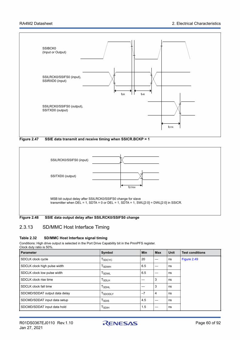
tSR tHR
tDTR
SSIBCK0(Input or Output)
SSILRCK0/SSIFS0 (input),SSIRXD0 (input)
SSILRCK0/SSIFS0 (output),SSITXD0 (output)
Figure 2.47 SSIE data transmit and receive timing when SSICR.BCKP = 1
tDTRW
SSILRCK0/SSIFS0 (input)
SSITXD0 (output)
MSB bit output delay after SSILRCK0/SSIFS0 change for slavetransmitter when DEL = 1, SDTA = 0 or DEL = 1, SDTA = 1, SWL[2:0] = DWL[2:0] in SSICR.
Figure 2.48 SSIE data output delay after SSILRCK0/SSIFS0 change
2.3.13 SD/MMC Host Interface Timing
Table 2.32 SD/MMC Host Interface signal timing Conditions: High drive output is selected in the Port Drive Capability bit in the PmnPFS register.Clock duty ratio is 50%.Parameter Symbol Min Max Unit Test conditions
SDCLK clock cycle TSDCYC 20 — ns Figure 2.49
SDCLK clock high pulse width TSDWH 6.5 — ns
SDCLK clock low pulse width TSDWL 6.5 — ns
SDCLK clock rise time TSDLH — 3 ns
SDCLK clock fall time TSDHL — 3 ns
SDCMD/SDDAT output data delay TSDODLY –7 4 ns
SDCMD/SDDAT input data setup TSDIS 4.5 — ns
SDCMD/SDDAT input data hold TSDIH 1.5 — ns
RA4M2 Datasheet 2. Electrical Characteristics
R01DS0367EJ0110 Rev.1.10Jan 27, 2021
Page 60 of 92

Note: Must use pins that have a letter appended to their name, for instance “_A”, “_B”, to indicate group membership. For the SD/MMCHost interface, the AC portion of the electrical characteristics is measured for each group.
SDnCLK(output)
SDnCMD/SDnDATm(input)
SDnCMD/SDnDATm(output)
TSDODLY(max)
TSDIS TSDIH
TSDLHTSDHL
TSDCYC
TSDWHTSDWL
TSDODLY(min)
n = 0, m = 0 to 3
Figure 2.49 SD/MMC Host Interface signal timing
2.4 USB Characteristics
2.4.1 USBFS Timing
Table 2.33 USBFS low-speed characteristics for host only (USB_DP and USB_DM pin characteristics) Conditions: VCC = AVCC0 = VCC_USB = VBATT = 3.0 to 3.6V, 2.7 ≤ VREFH0/VREFH ≤ AVCC0, USBCLK = 48 MHzParameter Symbol Min Typ Max Unit Test conditions
Inputcharacteristics
Input high voltage VIH 2.0 — — V —
Input low voltage VIL — — 0.8 V —
Differential input sensitivity VDI 0.2 — — V | USB_DP - USB_DM |
Differential common-mode range VCM 0.8 — 2.5 V —
Outputcharacteristics
Output high voltage VOH 2.8 — 3.6 V IOH = –200 µA
Output low voltage VOL 0.0 — 0.3 V IOL = 2 mA
Cross-over voltage VCRS 1.3 — 2.0 V Figure 2.50
Rise time tLR 75 — 300 ns
Fall time tLF 75 — 300 ns
Rise/fall time ratio tLR / tLF 80 — 125 % tLR/ tLF
Pull-up andpull-downcharacteristics
USB_DP and USB_DM pull-downresistance in host controller mode
Rpd 14.25 — 24.80 kΩ —
USB_DP,USB_DM
tLFtLR
90%10%10%
90%VCRS
Figure 2.50 USB_DP and USB_DM output timing in low-speed mode
RA4M2 Datasheet 2. Electrical Characteristics
R01DS0367EJ0110 Rev.1.10Jan 27, 2021
Page 61 of 92

Observation point
200 pF to 600 pF
USB_DP
USB_DM
200 pF to 600 pF
1.5 K
3.6 V27
Figure 2.51 Test circuit in low-speed mode
Table 2.34 USBFS full-speed characteristics (USB_DP and USB_DM pin characteristics) Conditions: VCC = AVCC0 = VCC_USB = VBATT = 3.0 to 3.6 V, 2.7 ≤ VREFH0/VREFH ≤ AVCC0, USBCLK = 48 MHzParameter Symbol Min Typ Max Unit Test conditions
Inputcharacteristics
Input high voltage VIH 2.0 — — V —
Input low voltage VIL — — 0.8 V —
Differential input sensitivity VDI 0.2 — — V | USB_DP - USB_DM |
Differential common-mode range VCM 0.8 — 2.5 V —
Outputcharacteristics
Output high voltage VOH 2.8 — 3.6 V IOH = –200 µA
Output low voltage VOL 0.0 — 0.3 V IOL = 2 mA
Cross-over voltage VCRS 1.3 — 2.0 V Figure 2.52
Rise time tLR 4 — 20 ns
Fall time tLF 4 — 20 ns
Rise/fall time ratio tLR / tLF 90 — 111.11 % tFR/ tFF
Output resistance ZDRV 28 — 44 Ω USBFS: Rs = 27 Ω included
Pull-up andpull-downcharacteristics
DM pull-up resistance in device controllermode
Rpu 0.900 — 1.575 kΩ During idle state
1.425 — 3.090 kΩ During transmission andreception
USB_DP and USB_DM pull-downresistance in host controller mode
Rpd 14.25 — 24.80 kΩ —
USB_DP,USB_DM
tFFtFR
90%10%10%
90%VCRS
Figure 2.52 USB_DP and USB_DM output timing in full-speed mode
RA4M2 Datasheet 2. Electrical Characteristics
R01DS0367EJ0110 Rev.1.10Jan 27, 2021
Page 62 of 92

Observation point
50 pF
50 pF
USB_DP
USB_DM
27
Figure 2.53 Test circuit in full-speed mode
Table 2.35 USBFS characteristics (USB_DP and USB_DM pin characteristics) Conditions: VCC = AVCC0 = VCC_USB = VBATT = 3.0 to 3.6 V, 2.7 ≤ VREFH0/VREFH ≤ AVCC0, USBCLK = 48 MHzParameter Symbol Min Typ Max Unit Test conditions
Battery ChargingSpecification
D+ sink current IDP_SINK 25 — 175 µA —
D- sink current IDM_SINK 25 — 175 µA —
DCD source current IDP_SRC 7 — 13 µA —
Data detection voltage VDAT_REF 0.25 — 0.4 V —
D+ source voltage VDP_SRC 0.5 — 0.7 V Outout current = 250 µA
D- source voltage VDM_SRC 0.5 — 0.7 V Outout current = 250 µA
2.5 ADC12 CharacteristicsTable 2.36 A/D conversion characteristics for unit 0 (1 of 2)Conditions: PCLKC = 1 to 50 MHzParameter Min Typ Max Unit Test conditions
Frequency 1 — 50 MHz —
Analog input capacitance — — 30 pF —
Quantization error — ±0.5 — LSB —
Resolution — — 12 Bits —
High-precision high-speedchannels(AN000 to AN002)
Conversion time*1
(operation at PCLKC =50 MHz)
Permissible signalsource impedanceMax. = 1 kΩ
0.52 (0.26)*2 — — μs Sampling in 13states
Max. = 400 Ω 0.40 (0.14)*2 — — μs Sampling in 7statesVCC = AVCC0 =3.0 to 3.6 V3.0 V ≤ VREFH0 ≤AVCC0
Offset error — ±1.0 ±2.5 LSB —
Full-scale error — ±1.0 ±2.5 LSB —
Absolute accuracy — ±2.0 ±4.5 LSB —
DNL differential nonlinearity error — ±0.5 ±1.5 LSB —
INL integral nonlinearity error — ±1.0 ±2.5 LSB —
RA4M2 Datasheet 2. Electrical Characteristics
R01DS0367EJ0110 Rev.1.10Jan 27, 2021
Page 63 of 92

Table 2.36 A/D conversion characteristics for unit 0 (2 of 2)Conditions: PCLKC = 1 to 50 MHzParameter Min Typ Max Unit Test conditions
High-precision normal-speedchannels(AN003 to AN008, AN011 toAN013)
Conversion time*1
(Operation at PCLKC =50 MHz)
Permissible signalsource impedanceMax. = 1 kΩ
0.92 (0.66)*2 — — μs Sampling in 33states
Offset error — ±1.0 ±2.5 LSB —
Full-scale error — ±1.0 ±2.5 LSB —
Absolute accuracy — ±2.0 ±4.5 LSB —
DNL differential nonlinearity error — ±0.5 ±1.5 LSB —
INL integral nonlinearity error — ±1.0 ±2.5 LSB —
Normal-precision normal-speedchannels (AN016)
Conversion time*1
(Operation at PCLKC =50 MHz)
Permissible signalsource impedanceMax. = 1 kΩ
0.92 (0.66)*2 — — μs Sampling in 33states
Offset error — ±1.0 ±5.5 LSB —
Full-scale error — ±1.0 ±5.5 LSB —
Absolute accuracy — ±2.0 ±7.5 LSB —
DNL differential nonlinearity error — ±0.5 ±4.5 LSB —
INL integral nonlinearity error — ±1.0 ±5.5 LSB —
Note: These specification values apply when there is no access to the external memory during A/D conversion. If access occurs duringA/D conversion, values might not fall within the indicated ranges.The use of PORT0 as digital outputs is not allowed when the 12-Bit A/D converter is used.The characteristics apply when AVCC0, AVSS0, VREFH0, VREFL0, and 12-bit A/D converter input voltage are stable.
Note 1. The conversion time includes the sampling and comparison times. The number of sampling states is indicated for the testconditions.
Note 2. Values in parentheses indicate the sampling time.
Table 2.37 A/D internal reference voltage characteristics
Parameter Min Typ Max Unit Test conditions
A/D internal reference voltage 1.13 1.18 1.23 V —
Sampling time 4.15 — — µs —
RA4M2 Datasheet 2. Electrical Characteristics
R01DS0367EJ0110 Rev.1.10Jan 27, 2021
Page 64 of 92

Integral nonlinearity error (INL)
Actual A/D conversion characteristic
Ideal A/D conversion characteristic
Analog input voltage
Offset error
Absolute accuracy
Differential nonlinearity error (DNL)
Full-scale error0xFFF
0x0000
Ideal line of actual A/D conversion characteristic
1-LSB width for ideal A/D conversion characteristic
Differential nonlinearity error (DNL)
1-LSB width for ideal A/D conversion characteristic
VREFH0(full-scale)
A/D converteroutput code
Figure 2.54 Illustration of ADC12 characteristic terms
Absolute accuracyAbsolute accuracy is the difference between output code based on the theoretical A/D conversion characteristics, and theactual A/D conversion result. When measuring absolute accuracy, the voltage at the midpoint of the width of the analoginput voltage (1-LSB width), which can meet the expectation of outputting an equal code based on the theoretical A/Dconversion characteristics, is used as an analog input voltage. For example, if 12-bit resolution is used and the referencevoltage VREFH0 = 3.072 V, then the 1-LSB width becomes 0.75 mV, and 0 mV, 0.75 mV, and 1.5 mV are used as theanalog input voltages. If the analog input voltage is 6 mV, an absolute accuracy of ±5 LSB means that the actual A/Dconversion result is in the range of 0x003 to 0x00D, though an output code of 0x008 can be expected from the theoreticalA/D conversion characteristics.
Integral nonlinearity error (INL)Integral nonlinearity error is the maximum deviation between the ideal line when the measured offset and full-scale errorsare zeroed, and the actual output code.
Differential nonlinearity error (DNL)Differential nonlinearity error is the difference between the 1-LSB width based on the ideal A/D conversion characteristicsand the width of the actual output code.
RA4M2 Datasheet 2. Electrical Characteristics
R01DS0367EJ0110 Rev.1.10Jan 27, 2021
Page 65 of 92

Offset errorOffset error is the difference between the transition point of the ideal first output code and the actual first output code.
Full-scale errorFull-scale error is the difference between the transition point of the ideal last output code and the actual last output code.
2.6 DAC12 CharacteristicsTable 2.38 D/A conversion characteristics
Parameter Min Typ Max Unit Test conditions
Resolution — — 12 Bits —
Without output amplifier
Absolute accuracy — — ±24 LSB Resistive load 2 MΩ
INL — ±2.0 ±8.0 LSB Resistive load 2 MΩ
DNL — ±1.0 ±2.0 LSB —
Output impedance — 8.5 — kΩ —
Conversion time — — 3 µs Resistive load 2 MΩ, Capacitive load 20 pF
Output voltage range 0 — VREFH V —
With output amplifier
INL — ±2.0 ±4.0 LSB —
DNL — ±1.0 ±2.0 LSB —
Conversion time — — 4.0 µs —
Resistive load 5 — — kΩ —
Capacitive load — — 50 pF —
Output voltage range 0.2 — VREFH – 0.2 V —
2.7 TSN CharacteristicsTable 2.39 TSN characteristics
Parameter Symbol Min Typ Max Unit Test conditions
Relative accuracy — — ± 1.0 — °C —
Temperature slope — — 4.0 — mV/°C —
Output voltage (at 25 °C) — — 1.24 — V —
Temperature sensor start time tSTART — — 30 µs —
Sampling time — 4.15 — — µs —
2.8 OSC Stop Detect CharacteristicsTable 2.40 Oscillation stop detection circuit characteristics
Parameter Symbol Min Typ Max Unit Test conditions
Detection time tdr — — 1 ms Figure 2.55
RA4M2 Datasheet 2. Electrical Characteristics
R01DS0367EJ0110 Rev.1.10Jan 27, 2021
Page 66 of 92

tdr
Main clock
OSTDSR.OSTDF
MOCO clock
ICLK
Figure 2.55 Oscillation stop detection timing
2.9 POR and LVD CharacteristicsTable 2.41 Power-on reset circuit and voltage detection circuit characteristics (1)
Parameter Symbol Min Typ MaxUnit Test conditions
Voltage detectionlevel
Power-on reset(POR)
DPSBYCR.DEEPCUT[1:0] = 00b or01b.
VPOR 2.5 2.6 2.7 V Figure 2.56
DPSBYCR.DEEPCUT[1:0] = 11b. 1.8 2.25 2.7
Voltage detection circuit (LVD0) Vdet0_1 2.84 2.94 3.04 Figure 2.57
Vdet0_2 2.77 2.87 2.97
Vdet0_3 2.70 2.80 2.90
Voltage detection circuit (LVD1) Vdet1_1 2.89 2.99 3.09 Figure 2.58
Vdet1_2 2.82 2.92 3.02
Vdet1_3 2.75 2.85 2.95
Voltage detection circuit (LVD2) Vdet2_1 2.89 2.99 3.09 Figure 2.59
Vdet2_2 2.82 2.92 3.02
Vdet2_3 2.75 2.85 2.95
Internal reset time Power-on reset time tPOR — 4.5 — ms Figure 2.56
LVD0 reset time tLVD0 — 0.51 — Figure 2.57
LVD1 reset time tLVD1 — 0.38 — Figure 2.58
LVD2 reset time tLVD2 — 0.38 — Figure 2.59
Minimum VCC down time*1 tVOFF 200 — — µs Figure 2.56,Figure 2.57
Response delay tdet — — 200 µs Figure 2.57 toFigure 2.59
LVD operation stabilization time (after LVD is enabled) td(E-A) — — 10 µs Figure 2.58,Figure 2.59
Hysteresis width (LVD1 and LVD2) VLVH — 70 — mV
Note 1. The minimum VCC down time indicates the time when VCC is below the minimum value of voltage detection levels VPOR, Vdet0,Vdet1, and Vdet2 for POR and LVD.
RA4M2 Datasheet 2. Electrical Characteristics
R01DS0367EJ0110 Rev.1.10Jan 27, 2021
Page 67 of 92

Internal reset signal(active-low)
VCC
tVOFF
tdet tPORtdettPORtdet
VPOR
Figure 2.56 Power-on reset timing
tVOFF
tLVD0tdet
Vdet0VCC
Internal reset signal(active-low)
tdet
VLVH
Figure 2.57 Voltage detection circuit timing (Vdet0)
RA4M2 Datasheet 2. Electrical Characteristics
R01DS0367EJ0110 Rev.1.10Jan 27, 2021
Page 68 of 92

tVOFF
Vdet1VCC
tdettdet
tLVD1
Td(E-A)
LVCMPCR.LVD1E
LVD1Comparator output
LVD1CR0.CMPE
LVD1SR.MON
Internal reset signal(active-low)
When LVD1CR0.RN = 0
When LVD1CR0.RN = 1
VLVH
tLVD1
Figure 2.58 Voltage detection circuit timing (Vdet1)
RA4M2 Datasheet 2. Electrical Characteristics
R01DS0367EJ0110 Rev.1.10Jan 27, 2021
Page 69 of 92

tVOFF
Vdet2VCC
tdettdet
tLVD2
Td(E-A)
LVCMPCR.LVD2E
LVD2Comparator output
LVD2CR0.CMPE
LVD2SR.MON
Internal reset signal (active-low)
When LVD2CR0.RN = 0
When LVD2CR0.RN = 1
VLVH
tLVD2
Figure 2.59 Voltage detection circuit timing (Vdet2)
2.10 VBATT Characteristics
Table 2.42 Battery backup function characteristics Conditions: VCC = AVCC0 = VCC_USB = 2.7 to 3.6 V, 2.7 ≤ VREFH0/VREFH ≤ AVCC0, VBATT = 1.8 to 3.6 VParameter Symbol Min Typ Max Unit Test conditions
Voltage level for switching to battery backup VDETBATT 2.50 2.60 2.70 V Figure 2.60
Lower-limit VBATT voltage for power supplyswitching caused by VCC voltage drop
VBATTSW 2.70 — — V
VCC-off period for starting power supplyswitching
tVOFFBATT 200 — — µs
VBATT low voltage detection level Vbattldet 1.8 1.9 2.0 V Figure 2.61
Minimum VBATT down time tBATTOFF 200 — — µs
Response delay tBATTdet — — 200 µs
VBATT monitor operation stabilization time(after VBATTMNSELR.VBATTMNSEL ischanged to 1)
td(E-A) — — 20 µs
VBATT current increase (whenVBATTMNSELR.VBATTMNSEL is 1 comparedto the case that VBATTMNSELR.VBATTMNSELis 0)
IVBATTSEL — 140 350 nA
Note: The VCC-off period for starting power supply switching indicates the period in which VCC is below the minimum value of the voltagelevel for switching to battery backup (VDETBATT).
RA4M2 Datasheet 2. Electrical Characteristics
R01DS0367EJ0110 Rev.1.10Jan 27, 2021
Page 70 of 92

VCC
tVOFFBATT
VDETBATT
VBATTSWVBATT
VCC supplyVBATT supplyVCC supplyBackup power area
Figure 2.60 Battery backup function characteristics
VBATT
tBATTOFF
Vbattldet
VBATTMON
tBATTdet tBATTdet
VBATTMNSEL
td(E-A)
Figure 2.61 Battery backup function characteristics
2.11 CTSU CharacteristicsTable 2.43 CTSU characteristics
Parameter Symbol Min Typ Max Unit Test conditions
External capacitance connected to TSCAP pin Ctscap 9 10 11 nF —
TS pin capacitive load Cbase — — 50 pF —
Permissible output high current ΣIoH — — -40 mA When the mutual capacitancemethod is applied
2.12 Flash Memory Characteristics
2.12.1 Code Flash Memory CharacteristicsTable 2.44 Code flash memory characteristics (1 of 2)Conditions: Program or erase: FCLK = 4 to 50 MHzRead: FCLK ≤ 50 MHz
Parameter Symbol
FCLK = 4 MHz 20 MHz ≤ FCLK ≤ 50 MHz
UnitTestconditionsMin Typ*6 Max Min Typ*6 Max
Programming timeNPEC ≤ 100 times
128-byte tP128 — 0.75 13.2 — 0.34 6.0 ms
8-KB tP8K — 49 176 — 22 80 ms
32-KB tP32K — 194 704 — 88 320 ms
RA4M2 Datasheet 2. Electrical Characteristics
R01DS0367EJ0110 Rev.1.10Jan 27, 2021
Page 71 of 92

Table 2.44 Code flash memory characteristics (2 of 2)Conditions: Program or erase: FCLK = 4 to 50 MHzRead: FCLK ≤ 50 MHz
Parameter Symbol
FCLK = 4 MHz 20 MHz ≤ FCLK ≤ 50 MHz
UnitTestconditionsMin Typ*6 Max Min Typ*6 Max
Programming timeNPEC > 100 times
128-byte tP128 — 0.91 15.8 — 0.41 7.2 ms
8-KB tP8K — 60 212 — 27 96 ms
32-KB tP32K — 234 848 — 106 384 ms
Erasure timeNPEC ≤ 100 times
8-KB tE8K — 78 216 — 43 120 ms
32-KB tE32K — 283 864 — 157 480 ms
Erasure timeNPEC > 100 times
8-KB tE8K — 94 260 — 52 144 ms
32-KB tE32K — 341 1040 — 189 576 ms
Reprogramming/erasure cycle*4 NPEC 10000*1 — — 10000*1 — — Times
Suspend delay during programming tSPD — — 264 — — 120 µs
Programming resume time tPRT — — 110 — — 50 µs
First suspend delay during erasure in suspendpriority mode
tSESD1 — — 216 — — 120 µs
Second suspend delay during erasure in suspendpriority mode
tSESD2 — — 1.7 — — 1.7 ms
Suspend delay during erasure in erasure prioritymode
tSEED — — 1.7 — — 1.7 ms
First erasing resume time during erasure in suspendpriority mode*5
tREST1 — — 1.7 — — 1.7 ms
Second erasing resume time during erasure insuspend priority mode
tREST2 — — 144 — — 80 µs
Erasing resume time during erasure in erasurepriority mode
tREET — — 144 — — 80 µs
Forced stop command tFD — — 32 — — 20 µs
Data hold time*2 tDRP 10*2 *3 — — 10*2 *3 — — Years
Note 1. This is the minimum number of times to guarantee all the characteristics after reprogramming. The guaranteed range is from 1 tothe minimum value.
Note 2. This indicates the minimum value of the characteristic when reprogramming is performed within the specified range.Note 3. This result is obtained from reliability testing.Note 4. The reprogram/erase cycle is the number of erasures for each block. When the reprogram/erase cycle is n times (n = 10,000),
erasing can be performed n times for each block. For example, when 128-byte programming is performed 64 times for differentaddresses in 8-KB blocks, and then the entire block is erased, the reprogram/erase cycle is counted as one. However, programmingthe same address several times as one erasure is not enabled. Overwriting is prohibited.
Note 5. Time for resumption includes time for reapplying the erasing pulse (up to one full pulse) that was cut off at the time of suspension.Note 6. The reference value at VCC = 3.3V and room temperature.
RA4M2 Datasheet 2. Electrical Characteristics
R01DS0367EJ0110 Rev.1.10Jan 27, 2021
Page 72 of 92

FACI command
FSTATR.FRDY
Programming pulse
• Suspension during programming
FACI command
FSTATR.FRDY
Erasure pulse
• Suspension during erasure in suspend priority mode
FACI command
FSTATR.FRDY
Erasure pulse
• Suspension during erasure in erasure priority mode
Program Suspend
Ready Not Ready Ready
Programming
tSPD
Erase Suspend
Ready Not Ready Ready
tSEED
Erasing
Erase Suspend Resume Suspend
Ready Not Ready Ready Not Ready
tSESD1 tSESD2
Erasing Erasing
tFD
• Forced Stop
FACI command
FSTATR.FRDY
Forced Stop
Not Ready Ready
Resume
tPRT
Programming
Resume
tREST1
Ready Not Ready
tREST2
Erasing
Resume
Not Ready
tREET
Erasing
Figure 2.62 Suspension and forced stop timing for flash memory programming and erasure
2.12.2 Data Flash Memory CharacteristicsTable 2.45 Data flash memory characteristics (1 of 2)Conditions: Program or erase: FCLK = 4 to 50 MHzRead: FCLK ≤ 50 MHz
Parameter Symbol
FCLK = 4 MHz 20 MHz ≤ FCLK ≤ 50 MHz
UnitTestconditionsMin Typ*6 Max Min Typ*6 Max
Programming time 4-byte tDP4 — 0.36 3.8 — 0.16 1.7 ms
8-byte tDP8 — 0.38 4.0 — 0.17 1.8
16-byte tDP16 — 0.42 4.5 — 0.19 2.0
Erasure time 64-byte tDE64 — 3.1 18 — 1.7 10 ms
128-byte tDE128 — 4.7 27 — 2.6 15
256-byte tDE256 — 8.9 50 — 4.9 28
Blank check time 4-byte tDBC4 — — 84 — — 30 µs
Reprogramming/erasure cycle*1 NDPEC 125000*2 — — 125000*2 — — —
Suspend delay during programming 4-byte tDSPD — — 264 — — 120 µs
8-byte — — 264 — — 120
16-byte — — 264 — — 120
Programming resume time tDPRT — — 110 — — 50 µs
First suspend delay during erasure insuspend priority mode
64-byte tDSESD1 — — 216 — — 120 µs
128-byte — — 216 — — 120
256-byte — — 216 — — 120
RA4M2 Datasheet 2. Electrical Characteristics
R01DS0367EJ0110 Rev.1.10Jan 27, 2021
Page 73 of 92

Table 2.45 Data flash memory characteristics (2 of 2)Conditions: Program or erase: FCLK = 4 to 50 MHzRead: FCLK ≤ 50 MHz
Parameter Symbol
FCLK = 4 MHz 20 MHz ≤ FCLK ≤ 50 MHz
UnitTestconditionsMin Typ*6 Max Min Typ*6 Max
Second suspend delay during erasure insuspend priority mode
64-byte tDSESD2 — — 300 — — 300 µs
128-byte — — 390 — — 390
256-byte — — 570 — — 570
Suspend delay during erasing in erasurepriority mode
64-byte tDSEED — — 300 — — 300 µs
128-byte — — 390 — — 390
256-byte — — 570 — — 570
First erasing resume time during erasure in suspendpriority mode*5
tDREST1 — — 300 — — 300 µs
Second erasing resume time during erasure insuspend priority mode
tDREST2 — — 126 — — 70 µs
Erasing resume time during erasure in erasurepriority mode
tDREET — — 126 — — 70 µs
Forced stop command tFD — — 32 — — 20 µs
Data hold time*3 tDRP 10*3 *4 — — 10*3 *4 — — Year
Note 1. The reprogram/erase cycle is the number of erasures for each block. When the reprogram/erase cycle is n times (n = 125,000),erasing can be performed n times for each block. For example, when 4-byte programming is performed 16 times for differentaddresses in 64-byte blocks, and then the entire block is erased, the reprogram/erase cycle is counted as one. However,programming the same address several times as one erasure is not enabled. Overwriting is prohibited.
Note 2. This is the minimum number of times to guarantee all the characteristics after reprogramming. The guaranteed range is from 1 tothe minimum value.
Note 3. This indicates the minimum value of the characteristic when reprogramming is performed within the specified range.Note 4. This result is obtained from reliability testing.Note 5. Time for resumption includes time for reapplying the erasing pulse (up to one full pulse) that was cut off at the time of suspension.Note 6. The reference value at VCC = 3.3 V and room temperature.
2.12.3 Option Setting Memory Characteristics
Table 2.46 Option setting memory characteristics Conditions: Program: FCLK = 4 to 50 MHzRead: FCLK ≤ 50 MHz
Parameter Symbol
FCLK = 4 MHz 20 MHz ≤ FCLK ≤ 50 MHz
Unit Test conditionsMin Typ*4 Max Min Typ*4 Max
Programming timeNOPC ≤ 100 times
tOP — 83 309 — 45 162 ms
Programming timeNOPC > 100 times
tOP — 100 371 — 55 195 ms
Reprogramming cycle NOPC 20000*1 — — 20000*1 — — Times
Data hold time*2 tDRP 10*2 *3 — — 10*2 *3 — — Years
Note 1. This is the minimum number of times to guarantee all the characteristics after reprogramming. The guaranteed range is from 1 tothe minimum value.
Note 2. This indicates the minimum value of the characteristic when reprogramming is performed within the specified range.Note 3. This result is obtained from reliability testing.Note 4. The reference value at VCC = 3.3 V and room temperature.
2.13 Boundary Scan
RA4M2 Datasheet 2. Electrical Characteristics
R01DS0367EJ0110 Rev.1.10Jan 27, 2021
Page 74 of 92

Table 2.47 Boundary scan characteristics
Parameter Symbol Min Typ Max Unit Test conditions
TCK clock cycle time tTCKcyc 100 — — ns Figure 2.63
TCK clock high pulse width tTCKH 45 — — ns
TCK clock low pulse width tTCKL 45 — — ns
TCK clock rise time tTCKr — — 5 ns
TCK clock fall time tTCKf — — 5 ns
TMS setup time tTMSS 20 — — ns Figure 2.64
TMS hold time tTMSH 20 — — ns
TDI setup time tTDIS 20 — — ns
TDI hold time tTDIH 20 — — ns
TDO data delay tTDOD — — 40 ns
Boundary scan circuit startup time*1 TBSSTUP tRESWP — — — Figure 2.65
Note 1. Boundary scan does not function until the power-on reset becomes negative.
tTCKcyc
tTCKH
tTCKf
tTCKLtTCKr
TCK
Figure 2.63 Boundary scan TCK timing
tTMSS tTMSH
tTDIS tTDIH
tTDOD
TCK
TMS
TDI
TDO
Figure 2.64 Boundary scan input/output timing
RA4M2 Datasheet 2. Electrical Characteristics
R01DS0367EJ0110 Rev.1.10Jan 27, 2021
Page 75 of 92

VCC
RES
Boundary scan execute
tBSSTUP
(= tRESWP)
Figure 2.65 Boundary scan circuit startup timing
2.14 Joint European Test Action Group (JTAG)
Table 2.48 JTAG
Parameter Symbol Min Typ Max Unit Test conditions
TCK clock cycle time tTCKcyc 40 — — ns Figure 2.66
TCK clock high pulse width tTCKH 15 — — ns
TCK clock low pulse width tTCKL 15 — — ns
TCK clock rise time tTCKr — — 5 ns
TCK clock fall time tTCKf — — 5 ns
TMS setup time tTMSS 8 — — ns Figure 2.67
TMS hold time tTMSH 8 — — ns
TDI setup time tTDIS 8 — — ns
TDI hold time tTDIH 8 — — ns
TDO data delay time tTDOD — — 20 ns
TCK
tTCKH
tTCKcyc
tTCKL
tTCKf
tTCKr
Figure 2.66 JTAG TCK timing
RA4M2 Datasheet 2. Electrical Characteristics
R01DS0367EJ0110 Rev.1.10Jan 27, 2021
Page 76 of 92

TCK
TMS
tTMSS tTMSH
TDI
tTDIS tTDIH
TDO
tTDOD
Figure 2.67 JTAG input/output timing
2.15 Serial Wire Debug (SWD)Table 2.49 SWD
Parameter Symbol Min Typ Max Unit Test conditions
SWCLK clock cycle time tSWCKcyc 40 — — ns Figure 2.68
SWCLK clock high pulse width tSWCKH 15 — — ns
SWCLK clock low pulse width tSWCKL 15 — — ns
SWCLK clock rise time tSWCKr — — 5 ns
SWCLK clock fall time tSWCKf — — 5 ns
SWDIO setup time tSWDS 8 — — ns Figure 2.69
SWDIO hold time tSWDH 8 — — ns
SWDIO data delay time tSWDD 2 — 28 ns
RA4M2 Datasheet 2. Electrical Characteristics
R01DS0367EJ0110 Rev.1.10Jan 27, 2021
Page 77 of 92
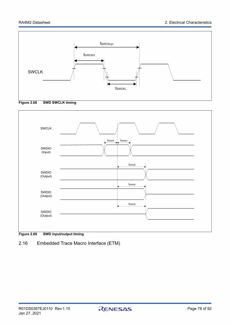
SWCLK
tSWCKH
tSWCKcyc
tSWCKL
Figure 2.68 SWD SWCLK timing
tSWDS
SWCLK
tSWDH
SWDIO(Input)
tSWDD
SWDIO(Output)
tSWDD
SWDIO(Output)
tSWDD
SWDIO(Output)
Figure 2.69 SWD input/output timing
2.16 Embedded Trace Macro Interface (ETM)
RA4M2 Datasheet 2. Electrical Characteristics
R01DS0367EJ0110 Rev.1.10Jan 27, 2021
Page 78 of 92
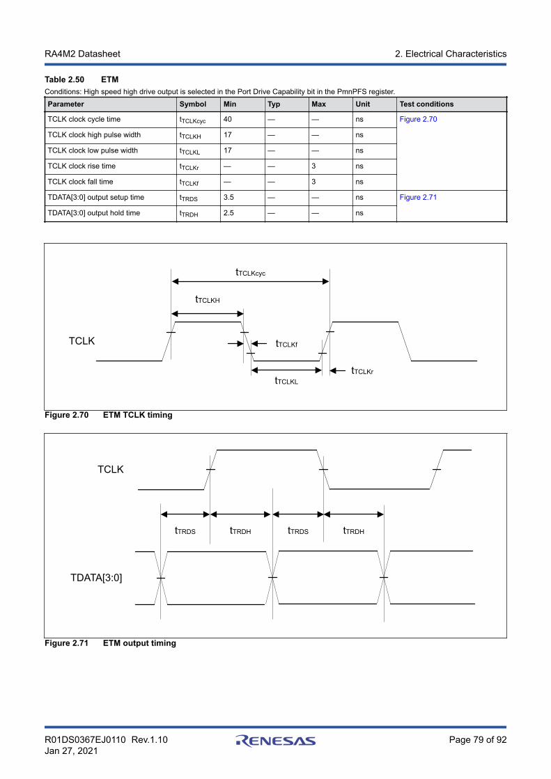
Table 2.50 ETM Conditions: High speed high drive output is selected in the Port Drive Capability bit in the PmnPFS register.Parameter Symbol Min Typ Max Unit Test conditions
TCLK clock cycle time tTCLKcyc 40 — — ns Figure 2.70
TCLK clock high pulse width tTCLKH 17 — — ns
TCLK clock low pulse width tTCLKL 17 — — ns
TCLK clock rise time tTCLKr — — 3 ns
TCLK clock fall time tTCLKf — — 3 ns
TDATA[3:0] output setup time tTRDS 3.5 — — ns Figure 2.71
TDATA[3:0] output hold time tTRDH 2.5 — — ns
TCLK
tTCLKH
tTCLKcyc
tTCLKL
tTCLKf
tTCLKr
Figure 2.70 ETM TCLK timing
TDATA[3:0]
TCLK
tTRDS tTRDStTRDH tTRDH
Figure 2.71 ETM output timing
RA4M2 Datasheet 2. Electrical Characteristics
R01DS0367EJ0110 Rev.1.10Jan 27, 2021
Page 79 of 92

Appendix 1. Port States in Each Processing Mode
Function Pin function Reset Software Standby modeDeep SoftwareStandby mode
After Deep Software Standbymode is canceled (return tostartup mode)
IOKEEP = 0 IOKEEP = 1*1
Mode MD Pull-up Keep-O Keep Hi-Z Keep
JTAG TCK/TMS/TDI Pull-up Keep-O Keep Hi-Z Keep
TDO output Keep-O Keep TDO output Keep
IRQ IRQx Hi-Z Keep-O*2 Keep Hi-Z Keep
IRQx-DS Hi-Z Keep-O*2 Keep*3 Hi-Z Keep
AGT AGTIOn Hi-Z Keep-O*2 Keep Hi-Z Keep
AGTIOn (n=1,3) Hi-Z Keep-O*2 Keep*3 Hi-Z Keep
SCI RXD0 Hi-Z Keep-O*2 Keep Hi-Z Keep
IIC SCLn/SDAn Hi-Z Keep-O*2 Keep Hi-Z Keep
USBFS USB_OVRCURx Hi-Z Keep-O*2 Keep Hi-Z Keep
USB_OVRCURx-DS/USB_VBUS
Hi-Z Keep-O*2 Keep*3 Hi-Z Keep
USB_DP/USB_DM Hi-Z Keep-O*4 Keep*3 Hi-Z Keep
RTC RTCICx Hi-Z Keep-O*2 Keep*3 Hi-Z Keep
RTCOUT Hi-Z [RTCOUT selected] RTCOUT output Keep Hi-Z Keep
CLKOUT CLKOUT Hi-Z [CLKOUT selected] CLKOUT output Keep Hi-Z Keep
DAC DAn Hi-Z [DAn output (DAOE = 1)] D/A output retained Keep Hi-Z Keep
Others — Hi-Z Keep-O Keep Hi-Z Keep
Note: H: High-levelL: Low-levelHi-Z: High-impedanceKeep-O: Output pins retain their previous values. Input pins go to high-impedance.Keep: Pin states are retained during periods in Software Standby mode.
Note 1. Retains the I/O port state until the DPSBYCR.IOKEEP bit is cleared to 0.Note 2. Input is enabled if the pin is specified as the Software Standby canceling source while it is used as an external interrupt pin.Note 3. Input is enabled if the pin is specified as the Deep Software Standby canceling source.Note 4. Input is enabled while the pin is used as an input pin.
RA4M2 Datasheet Appendix 1. Port States in Each Processing Mode
R01DS0367EJ0110 Rev.1.10Jan 27, 2021
Page 80 of 92
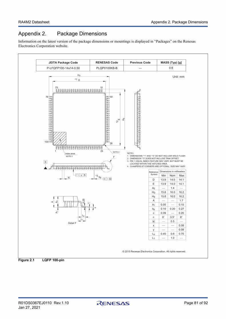
Appendix 2. Package DimensionsInformation on the latest version of the package dimensions or mountings is displayed in “Packages” on the RenesasElectronics Corporation website.
MASS (Typ) [g]
0.6
Unit: mm
Previous CodeRENESAS Code
PLQP0100KB-B —
JEITA Package Code
P-LFQFP100-14x14-0.50
© 2015 Renesas Electronics Corporation. All rights reserved.
DEA2
HD
HE
AA1
bp
c
exyLp
L1
13.913.9
15.815.8
0.050.150.090
0.45
Min NomDimensions in millimetersReference
Symbol Max14.014.01.416.016.0
0.20
3.50.5
0.61.0
14.114.1
16.216.21.7
0.150.270.208
0.080.080.75
NOTE)1. DIMENSIONS “*1” AND “*2” DO NOT INCLUDE MOLD FLASH.2. DIMENSION “*3” DOES NOT INCLUDE TRIM OFFSET.3. PIN 1 VISUAL INDEX FEATURE MAY VARY, BUT MUST BE LOCATED WITHIN THE HATCHED AREA.4. CHAMFERS AT CORNERS ARE OPTIONAL, SIZE MAY VARY.
HD
A2
A1
Lp
L1
Detail F
A c0.25
D
75
76
10026
251
50
51
F
NOTE 4
NOTE 3Index area
*1
HEE
*2
*3 bpey S
S
M
Figure 2.1 LQFP 100-pin
RA4M2 Datasheet Appendix 2. Package Dimensions
R01DS0367EJ0110 Rev.1.10Jan 27, 2021
Page 81 of 92
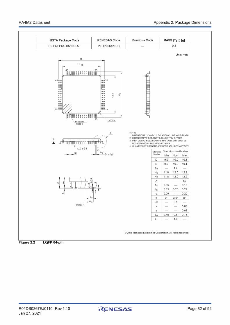
MASS (Typ) [g]
0.3
Unit: mm
Previous CodeRENESAS Code
PLQP0064KB-C —
JEITA Package Code
P-LFQFP64-10x10-0.50
© 2015 Renesas Electronics Corporation. All rights reserved.
DEA2
HD
HE
AA1
bp
c
exyLp
L1
9.99.9
11.811.8
0.050.150.090
0.45
Min NomDimensions in millimetersReference
Symbol Max10.010.01.412.012.0
0.20
3.50.5
0.61.0
10.110.1
12.212.21.7
0.150.270.208
0.080.080.75
NOTE)1. DIMENSIONS “*1” AND “*2” DO NOT INCLUDE MOLD FLASH.2. DIMENSION “*3” DOES NOT INCLUDE TRIM OFFSET.3. PIN 1 VISUAL INDEX FEATURE MAY VARY, BUT MUST BE LOCATED WITHIN THE HATCHED AREA.4. CHAMFERS AT CORNERS ARE OPTIONAL, SIZE MAY VARY.
HD
A2
A1
Lp
L1
Detail F
A c0.25
D
48 33
3249
17
161
64
F
NOTE 4
NOTE 3Index area
*1
HEE
*2
*3bpe
y S
S
M
Figure 2.2 LQFP 64-pin
RA4M2 Datasheet Appendix 2. Package Dimensions
R01DS0367EJ0110 Rev.1.10Jan 27, 2021
Page 82 of 92

MASS (Typ) [g]
0.2
Unit: mm
Previous CodeRENESAS Code
PLQP0048KB-B —
JEITA Package Code
P-LFQFP48-7x7-0.50
© 2015 Renesas Electronics Corporation. All rights reserved.
DEA2
HD
HE
AA1
bp
c
exyLp
L1
6.96.9
8.88.8
0.050.170.090
0.45
Min NomDimensions in millimetersReference
Symbol Max7.07.01.49.09.0
0.20
3.50.5
0.61.0
7.17.1
9.29.21.70.150.270.208
0.080.080.75
NOTE)1. DIMENSIONS “*1” AND “*2” DO NOT INCLUDE MOLD FLASH.2. DIMENSION “*3” DOES NOT INCLUDE TRIM OFFSET.3. PIN 1 VISUAL INDEX FEATURE MAY VARY, BUT MUST BE LOCATED WITHIN THE HATCHED AREA.4. CHAMFERS AT CORNERS ARE OPTIONAL, SIZE MAY VARY.
HD
A2
A1
Lp
L1
Detail F
A c0.25
HE
D
E
36 2525
24
13
37
48
1 12
F
NOTE 4
NOTE 3Index area
*1
*2
*3bpe
y S
S
M
Figure 2.3 LQFP 48-pin
RA4M2 Datasheet Appendix 2. Package Dimensions
R01DS0367EJ0110 Rev.1.10Jan 27, 2021
Page 83 of 92

INDEX AREA(D/2 X E/2)
D
SEATING PLANE
ccc C
bbb C A B
ddd C e b(48X)
E2
D2
L(48X) K(48X)
C
aaa C
B
2Xaaa C
(A3) A1A
eee C
fff C A B
fff C A B
A
EXPOSED DIE PAD
1 12
24
2536
37
48
E
13
2X
48X
36 25
13
121
48
37 24
ReferenceSymbol
Dimension in Millimeters
Min. Nom. Max.
A - - 0.80
A1 0.00 0.02 0.05
A3 0.203 REF.
b 0.20 0.25 0.30
D 7.00 BSC
E 7.00 BSC
e 0.50 BSC
L 0.30 0.40 0.50
K 0.20 - -
D2 5.25 5.30 5.35
E2 5.25 5.30 5.35
aaa 0.15
bbb 0.10
ccc 0.10
ddd 0.05
eee 0.08
fff 0.10
JEITA Package code RENESAS code MASS(TYP.)[g]
P-HWQFN048-7x7-0.50 PWQN0048KC-A 0.13 g
Figure 2.4 QFN 48-pin
RA4M2 Datasheet Appendix 2. Package Dimensions
R01DS0367EJ0110 Rev.1.10Jan 27, 2021
Page 84 of 92

Appendix 3. I/O RegistersThis appendix describes I/O register address and access cycles by function.
3.1 Peripheral Base AddressesThis section provides the base addresses for peripherals described in this manual. Table 3.1 shows the name, description,and the base address of each peripheral.
Table 3.1 Peripheral base address (1 of 3)
Name Description Base address
RMPU Renesas Memory Protection Unit 0x4000_0000
TZF TrustZone Filter 0x4000_0E00
SRAM SRAM Control 0x4000_2000
BUS BUS Control 0x4000_3000
DMAC0 Direct memory access controller 0 0x4000_5000
DMAC1 Direct memory access controller 1 0x4000_5040
DMAC2 Direct memory access controller 2 0x4000_5080
DMAC3 Direct memory access controller 3 0x4000_50C0
DMAC4 Direct memory access controller 4 0x4000_5100
DMAC5 Direct memory access controller 5 0x4000_5140
DMAC6 Direct memory access controller 6 0x4000_5180
DMAC7 Direct memory access controller 7 0x4000_51C0
DMA DMAC Module Activation 0x4000_5200
DTC Data Transfer Controller 0x4000_5400
ICU Interrupt Controller 0x4000_6000
CPSCU CPU System Security Control Unit 0x4000_8000
DBG Debug Function 0x400_1B000
FCACHE Flash Cache 0x400_1C100
SYSC System Control 0x4001_E000
PORT0 Port 0 Control Registers 0x4008_0000
PORT1 Port 1 Control Registers 0x4008_0020
PORT2 Port 2 Control Registers 0x4008_0040
PORT3 Port 3 Control Registers 0x4008_0060
PORT4 Port 4 Control Registers 0x4008_0080
PORT5 Port 5 Control Registers 0x4008_00A0
PORT6 Port 6 Control Registers 0x4008_00C0
PORT7 Port 7 Control Registers 0x4008_00E0
PORT8 Port 8 Control Registers 0x4008_0100
PORT9 Port9 Control Registers 0x40080120
PORTA Port A Control Registers 0x40080140
PORTB Port B Control Registers 0x40080160
PFS Pmn Pin Function Control Register 0x4008_0800
ELC Event Link Controller 0x4008_2000
RTC Realtime Clock 0x4008_3000
IWDT Independent Watchdog Timer 0x4008_3200
RA4M2 Datasheet Appendix 3. I/O Registers
R01DS0367EJ0110 Rev.1.10Jan 27, 2021
Page 85 of 92

Table 3.1 Peripheral base address (2 of 3)
Name Description Base address
WDT Watchdog Timer 0x4008_3400
CAC Clock Frequency Accuracy Measurement Circuit 0x4008_3600
MSTP Module Stop Control A, B, C, D 0x4008_4000
POEG Port Output Enable Module for GPT 0x4008_A000
USBFS USB 2.0 FS Module 0x4009_0000
SDHI0 SD Host Interface 0 0x4009_2000
SSIE0 Serial Sound Interface Enhanced (SSIE) 0x4009_D000
IIC0 Inter-Integrated Circuit 0 0x4009_F000
IIC0WU Inter-Integrated Circuit 0 Wake-up Unit 0x4009_F014
IIC1 Inter-Integrated Circuit 1 0x4009_F100
CAN0 CAN0 Module 0x400A_8000
CAN1 CAN1 Module 0x400A_9000
CTSU Capacitive Touch Sensing Unit 0x400D_0000
PSCU Peripheral Security Control Unit 0x400E_0000
AGT0 Low Power Asynchronous General purpose Timer 0 0x400E_8000
AGT1 Low Power Asynchronous General purpose Timer 1 0x400E_8100
AGT2 Low Power Asynchronous General purpose Timer 2 0x400E_8200
AGT3 Low Power Asynchronous General purpose Timer 3 0x400E_8300
AGT4 Low Power Asynchronous General purpose Timer 4 0x400E_8400
AGT5 Low Power Asynchronous General purpose Timer 5 0x400E_8500
TSN Temperature Sensor 0x400F_3000
CRC CRC Calculator 0x4010_8000
DOC Data Operation Circuit 0x4010_9000
SCI0 Serial Communication Interface 0 0x4011_8000
SCI1 Serial Communication Interface 1 0x4011_8100
SCI2 Serial Communication Interface 2 0x4011_8200
SCI3 Serial Communication Interface 3 0x4011_8300
SCI4 Serial Communication Interface 4 0x4011_8400
SCI9 Serial Communication Interface 9 0x4011_8900
SPI0 Serial Peripheral Interface 0 0x4011_A000
SCE9 Secure Cryptographic Engine 0x4016_1000
GPT320 General PWM 32-Bit Timer 0 0x4016_9000
GPT321 General PWM 32-Bit Timer 1 0x4016_9100
GPT322 General PWM 32-Bit Timer 2 0x4016_9200
GPT323 General PWM 32-Bit Timer 3 0x4016_9300
GPT164 General PWM 16-Bit Timer 4 0x4016_9400
GPT165 General PWM 16-Bit Timer 5 0x4016_9500
GPT166 General PWM 16-Bit Timer 6 0x4016_9600
GPT167 General PWM 16-Bit Timer 7 0x4016_9700
GPT_OPS Output Phase Switching Controller 0x4016_9A00
ADC120 12bit A/D Converter 0 0x4017_0000
RA4M2 Datasheet Appendix 3. I/O Registers
R01DS0367EJ0110 Rev.1.10Jan 27, 2021
Page 86 of 92

Table 3.1 Peripheral base address (3 of 3)
Name Description Base address
ADC121 12bit A/D Converter 1 0x4017_0200
DAC12 12-bit D/A converter 0x4017_1000
FLAD Data Flash 0x407F_C000
FACI Flash Application Command Interface 0x407F_E000
QSPI Quad-SPI 0x6400_0000
Note: Name = Peripheral nameDescription = Peripheral functionalityBase address = Lowest reserved address or address used by the peripheral
3.2 Access CyclesThis section provides access cycle information for the I/O registers described in this manual. Registers are grouped by associated module. The number of access cycles indicates the number of cycles based on the specified reference clock. In the internal I/O area, reserved addresses that are not allocated to registers must not be accessed, otherwise operations
cannot be guaranteed. The number of I/O access cycles depends on bus cycles of the internal peripheral bus, divided clock synchronization
cycles, and wait cycles of each module. Divided clock synchronization cycles differ depending on the frequency ratiobetween ICLK and PCLK.
When the frequency of ICLK is equal to that of PCLK, the number of divided clock synchronization cycles is alwaysconstant.
When the frequency of ICLK is greater than that of PCLK, at least 1 PCLK cycle is added to the number of dividedclock synchronization cycles.
The number of write access cycles indicates the number of cycles obtained by non-bufferable write access.
Note: This applies to the number of cycles when access from the CPU does not conflict with the instruction fetching to theexternal memory or bus access from other bus masters such as DTC or DMAC.
Table 3.2 Access cycles (1 of 3)
Peripherals
Address
Number of access cycles
ICLK = PCLK ICLK > PCLK*1CycleUnit Related functionFrom To Read Write Read Write
RMPU, TZF,SRAM, BUS,DMACn, DMA,DTC, ICU
0x4000_0000 0x4000_6FFF 2 2 2 2 ICLK Renesas MemoryProtection Unit,TrustZone Filter,SRAM Control, BUSControl, Directmemory accesscontroller n, DMACModule Activation,DTC Control Register,Interrupt Controller
CPSCU, DBG,FCACHE
0x4000_8000 0x4001_CFFF 4 3 4 3 ICLK CPU System SecurityControl Unit, DebugFunction, Flash Cache
SYSC 0x4001_E000 0x4001_E3FF 5 4 5 4 ICLK System Control
SYSC 0x4001_E400 0x4001_E5FF 9 8 5 to 8 5 to 8 PCLKB System Control
PORTn, PFS 0x4008_0000 0x4008_0FFF 5 4 2 to 5 2 to 4 PCLKB Port n ControlRegisters, Pmn PinFunction ControlRegister
RA4M2 Datasheet Appendix 3. I/O Registers
R01DS0367EJ0110 Rev.1.10Jan 27, 2021
Page 87 of 92

Table 3.2 Access cycles (2 of 3)
Peripherals
Address
Number of access cycles
ICLK = PCLK ICLK > PCLK*1CycleUnit Related functionFrom To Read Write Read Write
ELC, RTC, IWDT,WDT, CAC
0x4008_2000 0x4008_3FFF 5 4 3 to 5 2 to 4 PCLKB Event Link Controller,Realtime Clock,IndependentWatchdog Timer,Watchdog Timer,Clock FrequencyAccuracyMeasurement Circuit
MSTP 0x4008_4000 0x4008_4FFF 5 4 2 to 5 2 to 4 PCLKB Module Stop Control
POEG 0x4008_A000 0x4008_AFFF 5 4 3 to 5 2 to 4 PCLKB Port Output EnableModule for GPT
USBFS 0x4009_0000 0x4009_3FFF 6 5 3 to 6 3 to 5 PCLKB USB 2.0 FS Module
USBFS 0x4009_4000 0x4009_4FFF 4 3 1 to 4 1 to 3 PCLKB USB 2.0 FS Module
SDHI0, SSIE0,IICn, IIC0WU
0x4009_2000 0x4009_FFFF 5 4 2 to 5 2 to 4 PCLKB SD Host Interface 0,Serial Sound InterfaceEnhanced, Inter-Integrated Circuit n,Inter-Integrated Circuit0 Wake-up Unit
CANn 0x400A_8000 0x400A_9FFF 5 4 2 to 5 2 to 4 PCLKB CANn Module
CTSU 0x400D_0000 0x400D_FFFF 4 3 1 to 4 1 to 3 PCLKB Capacitive TouchSensing Unit
PSCU 0x400E_0000 0x400E_0FFF 5 4 2 to 5 2 to 4 PCLKB Peripheral SecurityControl Unit
AGTn 0x400E_8000 0x400E_8FFF 7 4 5 to 7 2 to 4 PCLKB Low PowerAsynchronousGeneral purposeTimer n
TSN 0x400F_3000 0x400F_3FFF 5 4 2 to 5 2 to 4 PCLKB Temperature Sensor
CRC, DOC 0x4010_8000 0x4010_9FFF 5 4 2 to 5 2 to 4 PCLKA CRC Calculator, DataOperation Circuit
SCIn 0x4011_8000 0x4011_8FFF 5*2 4*2 2 to 5*2 2 to 4*2 PCLKA Serial CommunicationInterface n
SPIn 0x4011_A000 0x4011_AFFF 5*3 4*3 2 to 5*3 2 to 4*3 PCLKA Serial PeripheralInterface n
SCE9 0x4016_1000 0x4016_1FFF 6 4 3 to 6 2 to 4 PCLKA Secure CryptographicEngine
GPT32n, GPT16n,GPT_OPS
0x4016_9000 0x4016_9FFF 7 4 4 to 7 2 to 4 PCLKA General PWM 32-BitTimer n, GeneralPWM 16-Bit Timer n,Output PhaseSwitching Controller
ADC12n, DAC12 0x4017_0000 0x4017_2FFF 5 4 2 to 5 2 to 4 PCLKA 12bit A/D Converter n,12-bit D/A converter
QSPI 0x6400_0000 0x6400_000F 5 14 to *4 2 to 5 14 to *4 PCLKA Quad-SPI
QSPI 0x6400_0010 0x6400_0013 25 to *4 6 to *4 25 to *4 5 to *4 PCLKA Quad-SPI
QSPI 0x6400_0014 0x6400_0037 5 14 to *4 2 to 5 14 to *4 PCLKA Quad-SPI
QSPI 0x6400_0804 0x6400_0807 4 3 1 to 4 1 to 3 PCLKA Quad-SPI
RA4M2 Datasheet Appendix 3. I/O Registers
R01DS0367EJ0110 Rev.1.10Jan 27, 2021
Page 88 of 92

Table 3.2 Access cycles (3 of 3)
Peripherals
Address
Number of access cycles
ICLK = FCLK ICLK > FCLK*1CycleUnit Related functionFrom To Read Write Read Write
FLAD, FACI 0x407F_C000 0x407F_EFFF 3 3 2 to 3 2 to 3 FCLK Data Flash, FlashApplication CommandInterface
Note 1. If the number of PCLK or FCLK cycles is non-integer (for example 1.5), the minimum value is without the decimal point, and themaximum value is rounded up to the decimal point. For example, 1.5 to 2. 5 is 1 to 3.
Note 2. When accessing a 16-bit register (FTDRHL, FRDRHL, FCR, FDR, LSR, and CDR), access is 2 cycles more than the value shown inTable 3.2. When accessing an 8-bit register (including FTDRH, FTDRL, FRDRH, and FRDRL), the access cycles are as shown inTable 3.2.
Note 3. When accessing the 32-bit register (SPDR), access is 2 cycles more than the value in Table 3.2. When accessing an 8-bit or 16-bitregister (SPDR_HA), the access cycles are as shown in Table 3.2.
Note 4. The access cycles depend on the QSPI bus cycles.
RA4M2 Datasheet Appendix 3. I/O Registers
R01DS0367EJ0110 Rev.1.10Jan 27, 2021
Page 89 of 92

Revision HistoryRevision 1.00 — August 28, 2020
First edition, issued
Revision 1.10 — January 27, 2021
1. Overview: Added note to Figure 1.1 Block diagram. Changed pin name in Table 1.15 Pin functions.
2. Electrical Characteristics: Added information about supported functions and pins. Changed LDO to LDOn in Table 2.7 Operating and standby current. added Note 15 to PLL2-LDO operating current in Table 2.7 Operating and standby current. Removed ADTRG1 in Figure 2.25 ADC12 trigger input timing.
RA4M2 Datasheet Revision History
R01DS0367EJ0110 Rev.1.10Jan 27, 2021
Page 90 of 92

General Precautions in the Handling of Microprocessing Unit and Microcontroller Unit Products The following usage notes are applicable to all Microprocessing unit and Microcontroller unit products from Renesas. For detailed usage notes on the
products covered by this document, refer to the relevant sections of the document as well as any technical updates that have been issued for the products.
1. Precaution against Electrostatic Discharge (ESD)
A strong electrical field, when exposed to a CMOS device, can cause destruction of the gate oxide and ultimately degrade the device operation. Steps
must be taken to stop the generation of static electricity as much as possible, and quickly dissipate it when it occurs. Environmental control must be
adequate. When it is dry, a humidifier should be used. This is recommended to avoid using insulators that can easily build up static electricity.
Semiconductor devices must be stored and transported in an anti-static container, static shielding bag or conductive material. All test and
measurement tools including work benches and floors must be grounded. The operator must also be grounded using a wrist strap. Semiconductor
devices must not be touched with bare hands. Similar precautions must be taken for printed circuit boards with mounted semiconductor devices. 2. Processing at power-on
The state of the product is undefined at the time when power is supplied. The states of internal circuits in the LSI are indeterminate and the states of
register settings and pins are undefined at the time when power is supplied. In a finished product where the reset signal is applied to the external reset
pin, the states of pins are not guaranteed from the time when power is supplied until the reset process is completed. In a similar way, the states of pins
in a product that is reset by an on-chip power-on reset function are not guaranteed from the time when power is supplied until the power reaches the
level at which resetting is specified. 3. Input of signal during power-off state
Do not input signals or an I/O pull-up power supply while the device is powered off. The current injection that results from input of such a signal or I/O
pull-up power supply may cause malfunction and the abnormal current that passes in the device at this time may cause degradation of internal
elements. Follow the guideline for input signal during power-off state as described in your product documentation. 4. Handling of unused pins
Handle unused pins in accordance with the directions given under handling of unused pins in the manual. The input pins of CMOS products are
generally in the high-impedance state. In operation with an unused pin in the open-circuit state, extra electromagnetic noise is induced in the vicinity of
the LSI, an associated shoot-through current flows internally, and malfunctions occur due to the false recognition of the pin state as an input signal
become possible. 5. Clock signals
After applying a reset, only release the reset line after the operating clock signal becomes stable. When switching the clock signal during program
execution, wait until the target clock signal is stabilized. When the clock signal is generated with an external resonator or from an external oscillator
during a reset, ensure that the reset line is only released after full stabilization of the clock signal. Additionally, when switching to a clock signal
produced with an external resonator or by an external oscillator while program execution is in progress, wait until the target clock signal is stable. 6. Voltage application waveform at input pin
Waveform distortion due to input noise or a reflected wave may cause malfunction. If the input of the CMOS device stays in the area between VIL
(Max.) and VIH (Min.) due to noise, for example, the device may malfunction. Take care to prevent chattering noise from entering the device when the
input level is fixed, and also in the transition period when the input level passes through the area between VIL (Max.) and VIH (Min.). 7. Prohibition of access to reserved addresses
Access to reserved addresses is prohibited. The reserved addresses are provided for possible future expansion of functions. Do not access these
addresses as the correct operation of the LSI is not guaranteed. 8. Differences between products
Before changing from one product to another, for example to a product with a different part number, confirm that the change will not lead to problems.
The characteristics of a microprocessing unit or microcontroller unit products in the same group but having a different part number might differ in terms
of internal memory capacity, layout pattern, and other factors, which can affect the ranges of electrical characteristics, such as characteristic values,
operating margins, immunity to noise, and amount of radiated noise. When changing to a product with a different part number, implement a system-
evaluation test for the given product.

© 2021 Renesas Electronics Corporation. All rights reserved.
Notice 1. Descriptions of circuits, software and other related information in this document are provided only to illustrate the operation of semiconductor products
and application examples. You are fully responsible for the incorporation or any other use of the circuits, software, and information in the design of your product or system. Renesas Electronics disclaims any and all liability for any losses and damages incurred by you or third parties arising from the useof these circuits, software, or information.
2. Renesas Electronics hereby expressly disclaims any warranties against and liability for infringement or any other claims involving patents, copyrights, or other intellectual property rights of third parties, by or arising from the use of Renesas Electronics products or technical information described in thisdocument, including but not limited to, the product data, drawings, charts, programs, algorithms, and application examples.
3. No license, express, implied or otherwise, is granted hereby under any patents, copyrights or other intellectual property rights of Renesas Electronicsor others.
4. You shall be responsible for determining what licenses are required from any third parties, and obtaining such licenses for the lawful import, export, manufacture, sales, utilization, distribution or other disposal of any products incorporating Renesas Electronics products, if required.
5. You shall not alter, modify, copy, or reverse engineer any Renesas Electronics product, whether in whole or in part. Renesas Electronics disclaims anyand all liability for any losses or damages incurred by you or third parties arising from such alteration, modification, copying or reverse engineering.
6. Renesas Electronics products are classified according to the following two quality grades: “Standard” and “High Quality”. The intended applications for each Renesas Electronics product depends on the product’s quality grade, as indicated below.
"Standard": Computers; office equipment; communications equipment; test and measurement equipment; audio and visual equipment; home electronic appliances; machine tools; personal electronic equipment; industrial robots; etc.
"High Quality": Transportation equipment (automobiles, trains, ships, etc.); traffic control (traffic lights); large-scale communication equipment; key financial terminal systems; safety control equipment; etc.
Unless expressly designated as a high reliability product or a product for harsh environments in a Renesas Electronics data sheet or other Renesas Electronics document, Renesas Electronics products are not intended or authorized for use in products or systems that may pose a direct threat to human life or bodily injury (artificial life support devices or systems; surgical implantations; etc.), or may cause serious property damage (space system; undersea repeaters; nuclear power control systems; aircraft control systems; key plant systems; military equipment; etc.). Renesas Electronics disclaims any and all liability for any damages or losses incurred by you or any third parties arising from the use of any Renesas Electronics product that is inconsistent with any Renesas Electronics data sheet, user’s manual or other Renesas Electronics document.
7. No semiconductor product is absolutely secure. Notwithstanding any security measures or features that may be implemented in Renesas Electronics hardware or software products, Renesas Electronics shall have absolutely no liability arising out of any vulnerability or security breach, including butnot limited to any unauthorized access to or use of a Renesas Electronics product or a system that uses a Renesas Electronics product. RENESAS ELECTRONICS DOES NOT WARRANT OR GUARANTEE THAT RENESAS ELECTRONICS PRODUCTS, OR ANY SYSTEMS CREATED USING RENESAS ELECTRONICS PRODUCTS WILL BE INVULNERABLE OR FREE FROM CORRUPTION, ATTACK, VIRUSES, INTERFERENCE, HACKING, DATA LOSS OR THEFT, OR OTHER SECURITY INTRUSION (“Vulnerability Issues”). RENESAS ELECTRONICS DISCLAIMS ANY AND ALL RESPONSIBILITY OR LIABILITY ARISING FROM OR RELATED TO ANY VULNERABILITY ISSUES. FURTHERMORE, TO THE EXTENT PERMITTED BY APPLICABLE LAW, RENESAS ELECTRONICS DISCLAIMS ANY AND ALL WARRANTIES, EXPRESS OR IMPLIED, WITH RESPECT TO THIS DOCUMENT AND ANY RELATED OR ACCOMPANYING SOFTWARE OR HARDWARE, INCLUDING BUT NOT LIMITED TO THE IMPLIED WARRANTIES OF MERCHANTABILITY, OR FITNESS FOR A PARTICULAR PURPOSE.
8. When using Renesas Electronics products, refer to the latest product information (data sheets, user’s manuals, application notes, “General Notes for Handling and Using Semiconductor Devices” in the reliability handbook, etc.), and ensure that usage conditions are within the ranges specified by Renesas Electronics with respect to maximum ratings, operating power supply voltage range, heat dissipation characteristics, installation, etc. RenesasElectronics disclaims any and all liability for any malfunctions, failure or accident arising out of the use of Renesas Electronics products outside of such specified ranges.
9. Although Renesas Electronics endeavors to improve the quality and reliability of Renesas Electronics products, semiconductor products have specificcharacteristics, such as the occurrence of failure at a certain rate and malfunctions under certain use conditions. Unless designated as a high reliability product or a product for harsh environments in a Renesas Electronics data sheet or other Renesas Electronics document, Renesas Electronics products are not subject to radiation resistance design. You are responsible for implementing safety measures to guard against the possibility of bodily injury, injury or damage caused by fire, and/or danger to the public in the event of a failure or malfunction of Renesas Electronics products, such as safety design for hardware and software, including but not limited to redundancy, fire control and malfunction prevention, appropriate treatment foraging degradation or any other appropriate measures. Because the evaluation of microcomputer software alone is very difficult and impractical, you areresponsible for evaluating the safety of the final products or systems manufactured by you.
10. Please contact a Renesas Electronics sales office for details as to environmental matters such as the environmental compatibility of each Renesas Electronics product. You are responsible for carefully and sufficiently investigating applicable laws and regulations that regulate the inclusion or use of controlled substances, including without limitation, the EU RoHS Directive, and using Renesas Electronics products in compliance with all these applicable laws and regulations. Renesas Electronics disclaims any and all liability for damages or losses occurring as a result of your noncompliance with applicable laws and regulations.
11. Renesas Electronics products and technologies shall not be used for or incorporated into any products or systems whose manufacture, use, or sale isprohibited under any applicable domestic or foreign laws or regulations. You shall comply with any applicable export control laws and regulations promulgated and administered by the governments of any countries asserting jurisdiction over the parties or transactions.
12. It is the responsibility of the buyer or distributor of Renesas Electronics products, or any other party who distributes, disposes of, or otherwise sells or transfers the product to a third party, to notify such third party in advance of the contents and conditions set forth in this document.
13. This document shall not be reprinted, reproduced or duplicated in any form, in whole or in part, without prior written consent of Renesas Electronics.14. Please contact a Renesas Electronics sales office if you have any questions regarding the information contained in this document or Renesas
Electronics products.
(Note1) “Renesas Electronics” as used in this document means Renesas Electronics Corporation and also includes its directly or indirectly controlled subsidiaries.
(Note2) “Renesas Electronics product(s)” means any product developed or manufactured by or for Renesas Electronics.
(Rev.5.0-1 October 2020)
Corporate Headquarters Contact information TOYOSU FORESIA, 3-2-24 Toyosu, Koto-ku, Tokyo 135-0061, Japan www.renesas.com
For further information on a product, technology, the most up-to-date version of a document, or your nearest sales office, please visit: www.renesas.com/contact/.
Trademarks Renesas and the Renesas logo are trademarks of Renesas Electronics Corporation. All trademarks and registered trademarks are the property of their respective owners.