SM2400 Bootloader User Guide - Adesto Technologies Downloading code images to internal memory from...
20
AD-SM2400AP02A-PWRLN-8/2016 Overview This application note describes the SM2400 Bootloader modes, interface, and protocols, and includes programming examples. AD-SM2400AP02A-PWRLN SM2400 Bootloader User Guide Revision 1.0 August 2016 Communication Technology by: Semitech Semiconductor Application Note
Transcript of SM2400 Bootloader User Guide - Adesto Technologies Downloading code images to internal memory from...

AD-SM2400AP02A-PWRLN
SM2400 Bootloader User Guide
Revision 1.0August 2016
Communication Technology by:Semitech SemiconductorApplication Note
Overview
This application note describes the SM2400 Bootloader modes, interface, and protocols, and includes programming examples.
AD-SM2400AP02A-PWRLN-8/2016
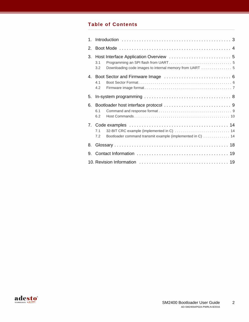
Table of Contents
1. Introduction . . . . . . . . . . . . . . . . . . . . . . . . . . . . . . . . . . . . . . . . . . . . 3
2. Boot Mode . . . . . . . . . . . . . . . . . . . . . . . . . . . . . . . . . . . . . . . . . . . . . 4
3. Host Interface Application Overview . . . . . . . . . . . . . . . . . . . . . . . . . 53.1 Programming an SPI flash from UART . . . . . . . . . . . . . . . . . . . . . . . . . . . . . . . 5
3.2 Downloading code images to internal memory from UART . . . . . . . . . . . . . . . 5
4. Boot Sector and Firmware Image . . . . . . . . . . . . . . . . . . . . . . . . . . . 64.1 Boot Sector Format. . . . . . . . . . . . . . . . . . . . . . . . . . . . . . . . . . . . . . . . . . . . . . 6
4.2 Firmware image format . . . . . . . . . . . . . . . . . . . . . . . . . . . . . . . . . . . . . . . . . . . 7
5. In-system programming . . . . . . . . . . . . . . . . . . . . . . . . . . . . . . . . . . . 8
6. Bootloader host interface protocol . . . . . . . . . . . . . . . . . . . . . . . . . . . 96.1 Command and response format . . . . . . . . . . . . . . . . . . . . . . . . . . . . . . . . . . . . 9
6.2 Host Commands . . . . . . . . . . . . . . . . . . . . . . . . . . . . . . . . . . . . . . . . . . . . . . . 10
7. Code examples . . . . . . . . . . . . . . . . . . . . . . . . . . . . . . . . . . . . . . . . 147.1 32-BIT CRC example (implemented in C) . . . . . . . . . . . . . . . . . . . . . . . . . . . 14
7.2 Bootloader command transmit example (implemented in C) . . . . . . . . . . . . . 14
8. Glossary . . . . . . . . . . . . . . . . . . . . . . . . . . . . . . . . . . . . . . . . . . . . . . 18
9. Contact Information . . . . . . . . . . . . . . . . . . . . . . . . . . . . . . . . . . . . . 19
10. Revision Information . . . . . . . . . . . . . . . . . . . . . . . . . . . . . . . . . . . . 19
2SM2400 Bootloader User Guide AD-SM2400AP02A-PWRLN-8/2016

1. Introduction
The SM2400 bootloader is executed when the SM2400 modem comes out of reset. Based on the SM2400 modem mode pins (described in Section 2.), the bootloader can perform the following functions:
Direct execution toward a flash memory device or external SRAM
Read and write data to the external flash
Read and write data to internal and external memory
Enter debugger mode
3SM2400 Bootloader User Guide AD-SM2400AP02A-PWRLN-8/2016

2. Boot Mode
The boot mode is determined by the state of the SM2400 mode pins (MODE0, MODE1 and MODE2) immediately after reset. The values are latched when reset is de-activated, and the pins can be used as general-purpose IOs after the boot sequence. The mode combinations are shown in Table 2-1.
In the Boot from SPI mode, the bootloader will look for a valid firmware image in the external flash. The format of the firmware image is detailed in Section 4.2. If the boot mode is not valid or booting from an image fails, the device will time out after 10 seconds and reset. This is to prevent the case where the boot image fails due to a spurious error on the read values, so a reset and new read should allow the system to recover.
In the host interface modes, an external host can send commands to the device to access internal and external memory, including writing to an external flash memory. The framing formats are described in Section 6.1, and the available commands in Section 6.2.
The debug modes are not described in this document.
Table 2-1. Boot Modes
Boot Mode MODE[2:0] Pins
Boot from SPI 000
Host Interface on SPI 001
Host Interface on UART 010
Boot from external memory 011
Reserved 100
Reserved 101
DLL and PHY debug mode 110
DLL debug mode 111
4SM2400 Bootloader User Guide AD-SM2400AP02A-PWRLN-8/2016

3. Host Interface Application Overview
This section contains overviews of example applications of the host interface.
3.1 Programming an SPI flash from UART
When programming an SPI flash device from the UART, the SPI interface to the flash device is configured as a pass-through from the UART.
These steps should be followed:
1. Perform a reset with the SM2400 mode pins set to 010.
2. Set UART bit rate to 2400 bps.
3. Send UART configuration command to configure the SM2400 UART to higher bit rate (using the Configure UART0 command described in Section 6.2.4).
4. Change the local UART bit rate to the higher rate.
5. Configure the SPI interface (using the Configure SPI1 Pass Through command described in Section 6.2.7).
6. Send commands to SPI flash (using the SPI1 Command command described in Section 6.1.2).
7. Perform a reset with the SM2400 mode pins set to 000 (to boot from flash).
3.2 Downloading code images to internal memory from UART
When downloading firmware images to the internal memory, the bootloader accepts blocks of data and stores them in memory. Once all the memory is populated, an Execute command is issued to start the execution.
These steps should be followed:
1. Perform a reset with the SM2400 mode pins set to 010.
2. Set UART bit rate to 2400 bps.
3. Send UART configuration command to configure the SM2400 UART to higher bit rate (using the Configure UART0 command described in Section 6.2.4).
4. Change the local UART bit rate to the higher rate.
5. Parse the *.bundle file (see Section 4.):
a. Locate the boot sector at the beginning of the file, which includes the location of the firmware image.
b. Parse the image header to get the execution start addresses and the CRC.
c. Parse the address table.
d. Locate the memory blocks within the *.bundle file.
6. Write the memory blocks into SM2400 internal memory (using the Write command described in Section 6.2.5).
7. Calculate the 32-bit CRC using the first 24 bytes of the image header and the memory blocks (not the address table). It should match the 1-s complement of the CRC in the image header.
8. Send the DLL and PHY start addresses to the SM2400 modem and start the execution (using the Execute command described in Section 6.2.10).
5SM2400 Bootloader User Guide AD-SM2400AP02A-PWRLN-8/2016

4. Boot Sector and Firmware Image
The boot sector and the firmware image contain all the information and the data necessary for the bootloader or a host to download the firmware image to be executed. Those components should either reside on an external SPI flash to be read by the bootloader or provided to the host to boot the SM2400 from the host interface. The boot sector and a respective image are packaged in a *.bundle file that can be read by the host or programmed onto an SPI flash. The following sections describe in detail the format of the different components of a *.bundle file."
4.1 Boot Sector Format
The purpose of the Boot Sector is to either specify a location of the firmware to be loaded into the PHY and DLL, or to specify details of a host interface for the receipt of subsequent commands.
4.1.1 Boot Sector characteristics
The Boot Sector is 32 bytes long, with the following fields in the order shown below:
Magic number:
4 bytes, 0xb00753c7 (big-endian)
Identifies this sector as a boot sector
CRC-8 of Boot Sector, excluding Magic number, 1 byte
Location of Next Boot Sector:
The upper 3 bits determine where the next candidate boot sector is. The offset between the two candidate boot sectors is given by 4 KB multiplied by 2 to the power of this value.
The lower 5 bits indicate the Boot device. These should be set to 4 for SPI1 SS0.
Device configuration: 6 bytes (see below).
Image Sequence number,1 byte: this is set to 0 for the first boot sector, to 1 for the second
Reserved field of 7 bytes.
Device Tag: 8 bytes, general information to be written to the top of DRAM on the DLL.
Location of firmware image: 4 bytes, an absolute address into the boot device above.
4.1.2 Device configuration bytes
Below are details of device configuration bytes (big-endian) for the SPI flash (SPI1 register):
Bits 31 - 29: Number of dummy bytes after command
Bits 28 - 24: Max page size for read. Page size is two to the power of this value. If 0, only single byte reads.
Bits 23 - 16: Read command
Bit 15: Clock polarity (CPOL)
Bit 14: Clock phase (CPHA)
Bits 13 - 12: Address width minus 2. So 0 means 2 byte address;1 means 3-byte address. Only 2- and 3-byte addresses are valid.
Bit 11: Set to 1.
Bits 10 - 0: The SPI frequency clock rate divisor (divisor = 6 x 10⁷/ SPI CLK). MAX SPI CLK = 7.5MHz.
6SM2400 Bootloader User Guide AD-SM2400AP02A-PWRLN-8/2016

4.2 Firmware image format
The firmware image, which in many cases would follow the boot sector, is composed of the Image Header and the binary code. These are needed when booting from SPI or external memory.
4.2.1 Image Header
The Image Header consists of the following:
Firmware ID: 4 bytes; this is for product differentiation, since the bootloader will only load firmware for a specific ID. By default the Firmware ID is set to 0xb0240000, big-endian. The 0xb024 is for SM2400; the last two bytes may be used for differentiation.
ROM major rev: 1 byte - value 0x05
ROM minor rev: 1 byte - value 0x00
User ID: 2 bytes; this is for customized user purposes. For example, this field can be used if an application boots a specific firmware from a list of bootable images residing in the SPI flash.
DLL Execution start address: 4 bytes, big-endian
PHY Execution start address: 4 bytes, big-endian
DLL VECBASE address: 4 bytes, big-endian
PHY VECBASE address: 4 bytes, big-endian
CRC-32 of the Image Header and the loaded firmware sections (calculated in order as specified in the ROM store table): 4 bytes; MSB is highest coefficient. The generating polynomial is 0x104C11DB7; the least significant bit is shifted in first.
The binary code, starting with the ROM store table.
Note: The DLL and PHY execution start addresses must be aligned to 4-byte boundaries.
Note: The DLL and PHY VECBASE addresses must be aligned to 1024-byte boundaries.
4.2.2 Address Table
The image header is followed by an address table with the following three 4-byte big-endian addresses:
Target base address in SM2400 memory
Target top address in SM2400 memory
Location in firmware image relative to the Location of Firmware Image address (see Section 4.1.1).
The last entry in the address table is followed by 12 bytes of zeroes.
4.2.3 Code segments
The code segments are located above the address table without any specific framing. Although each code segment starts at a 4-byte boundary, some code segments may have a length that is not a multiple of 4 bytes.
7SM2400 Bootloader User Guide AD-SM2400AP02A-PWRLN-8/2016

5. In-system programming
The bootloader supports in-system programming of external code memories (SPI EEPROM, SPI flash, external flash, or external RAM) by using the host interface.
This feature can be used at board assembly time to program the latest firmware and boot sector during final test.
8SM2400 Bootloader User Guide AD-SM2400AP02A-PWRLN-8/2016

6. Bootloader host interface protocol
6.1 Command and response format
Commands and responses through the Host Interface UART0 are formatted as described below.
6.1.1 UART
The default bit rate of the UART is 2400 bps. It can be changed using the Configure UART0 command described in Section 6.2.
6.1.1.1 Command from Host:
6.1.1.2 Response from SM2400:
6.1.1.3 Key definitions and comments:
Start of Frame is a fixed two-byte code of 0x9B 0xFE.
Command is the command code.
Length is the number of bytes in the Data field. The maximum length is 72 bytes.
Return status is a one-byte code that indicates the result of the command:
0x00 - Success
0xFE - CRC Error, Data contains expected CRC
Others - Detailed under each command
Data bytes contain the value of parameters (for a command), or return values (for a response); this section is optional depending on the command.
CRC-16 is a two-byte CRC calculated for all the information in the command except for the Start of Frame bytes. The CRC coefficients are x16 + x12 + x5 + 1; MSB is the highest coefficient.
0x9B (ASCII ESC) is used as an escape character to precede control characters. Thus the literal 0x9B itself, if it occurs in data, needs to be represented by an escape sequence, which is 0x9B 0x64 (0x64 being the inverse of 0x9B).
Note: Escape processing is done after the application of CRC-16. That is, CRC-16 is applied to the raw unescaped data, and then the final binary string is escape stuffed where required, including the two-byte CRC-16 itself.
6.1.2 SPI
SPI is similar to UART, but the command and response are contained in a single transaction with wait states inserted in between. The wait state is indicated by returning bytes of 0xFF (which would be an invalid return status and length combination). Framing and escape stuffing in SPI is the same as for UART.
Start of Frame Command/Length (MS bits) Length (LS bits) Data (optional) CRC-16
2 bytes 1 byte 1 byte Variable bytes 2 bytes
Return Status/Length (MS bits) Length (LS bits) Data (optional) CRC-16
1 byte 1 byte Variable bytes 2 bytes
9SM2400 Bootloader User Guide AD-SM2400AP02A-PWRLN-8/2016

6.1.2.1 MOSI:
6.1.2.2 MISO:
6.2 Host Commands
In order to use the SPI master and/or the external memory, they must be configured first using respective command(s). Until configured properly, they will remain disabled. Because of this, external memory must be enabled before it can be accessed at any stage (read, write, boot image commands).
6.2.1 0x00 - Firmware ID
As defined under Boot Sector Format (Section 4.1).
6.2.2 0x01 - Obsolete ROM rev
Return the ROM version for which any earlier firmware versions are obsolete and will not be loaded.
6.2.3 0x02 - ROM rev
Return the ROM revision number as defined under Boot Sector Format (Section 4.1).
Start of Frame Command Length Data (optional) CRC-16 Wait States Dummy bytes
2 bytes 1 byte 1 byte Variable bytes 2 bytes Variable bytes Variable
(Command and Wait States) Return Status Length Data (optional) CRC-16
(as above) 1 byte 1 byte Variable bytes 2 bytes
Command Data
0x00 None
Return Status Data
0x00 - Success 4 bytes (Currently, 0xb0240000 - SM2400)
Command Data
0x01 None
Return Status Data
0x00 - success Obsolete ROM Major number (1 byte) Obsolete ROM Minor number (1 byte)
Command Data
0x02 None
Return Status Data
0x00 - Success Major number (1 byte) Minor number (1 byte)
10SM2400 Bootloader User Guide AD-SM2400AP02A-PWRLN-8/2016
6.2.4 0x03 - Configure UART0
Configure the UART0 Host interface.
6.2.5 0x04 - Write
Write to 32-bit aligned address specified.
6.2.6 0x05 - Read
Read from 32-bit aligned address specified.
6.2.7 0x06 - SPI1 pass through
Configure SPI1 pass through.
Command Data
0x03 2 bytes (big-endian)
Bit 15: Hardware handshaking OFF (0) or ON (1)
Bits 14 - 0: Baud rate divisor to generate the baud clock (16X baud rate) divisor
[divisor = 6 x 10⁷ + (Baud x 8) / Baud x16]
Return Status Data
0x00 - Success
0x01 - Invalid configuration
None
Command Data
0x04 Address (4 bytes, 32-bit-aligned, big-endian) Data to be written (variable length, multiple of 4 bytes, up to max command length)
Return Status Data
0x00 - Success
0x01 - Error
None
Command Data
0x05 Address (4 bytes, 32-bit aligned big-endian) Number of bytes to read, number being a multiple of 4 (1 byte) 1 - 64
Return Status Data
0x00 - Success
0x01 - Error
Data Read (variable length) None
Command Data
0x06 Set Slave number (1 byte) Clock Mode (1 byte)
Bit 7: Clock Polarity (CPOL)
Bit 6: Clock Phase (CPHA)
Clock divisor (2 bytes)
Bit 15 - 0: Clock rate divisor
[divisor = 6 x 10⁷/ SPI CLK]
MAX SPI CLK = 7.5MHz
11SM2400 Bootloader User Guide AD-SM2400AP02A-PWRLN-8/2016

6.2.8 0x07 - SPI1 command
Execute a command through SPI1.
6.2.9 0x08 - Configure Ext Mem
Configure the external memory CS0 interface.
6.2.10 0x09 - Execute
Pass execution to the firmware at given address - that, is jump to address.
Note: The dynamic vectors are not changed before jumping to the addresses given. They will be set to ROM addresses (because this is what the bootloader uses). It is assumed that the vectors are set by the user program.
Return Status Data
0x00 - Success None
Command Data (bytes)
0x07 Length of Read phase (2 bytes, big-endian) Command bytes (variable length)
Return Status Data
0x00 - Success Data from Read phase (variable length)
Command Data (bytes)
0x08 Mem Type (1 byte) Bit 6:
SRAM (0) or Flash (1)
Static Timing Register Value register as defined in synopsis designware static memory controller databook, byte-swapped (4 bytes)
FLASH Timing register as defined in synopsis designware static memory controller databook, byte-swapped (2 bytes)
Return Status Data
0x00 - Success
0x01 - Invalid configuration
None
Command Data (bytes) Data (bytes)
0x09 DLL Address to jump to (4 bytes, big-endian)
PHY Address to jump to (4 bytes, big-endian)
Return Status Data
0x00 - Success
0x01 - Error
None
12SM2400 Bootloader User Guide AD-SM2400AP02A-PWRLN-8/2016

6.2.11 0x0A - CRC32
Return the CRC-32 of a given block of data.
6.2.12 0x0B - BOOT_IMAGE:
Boot from image specified.
Note: The dynamic vectors are changed based on the values in the firmware image header before jumping to execution.
6.2.13 0x0C - RESET
Reset the DLL processor.
Note: This will not return and will cause both the DLL and PHY to reset.
Command Data (bytes)
0x0A Initial CRC (4 bytes) Start Address of block(4 bytes, big-endian)
Block size (4 bytes, big-endian)
Return Status Data
0x00 - Success
0x01 - Error
CRC-32 (4 bytes)
None
Command Data (bytes)
0x0B Boot device number as defined in the Boot Sector (1 byte)
Device Config as defined in the Boot Sector (6 bytes, big-endian)
Location of image to boot from in the device i.e the Image Address (4 bytes, big-endian)
Return Status Data
0x00 - Success
0x01 - Error
None
Command Data (bytes)
0x0C none
Return Status Data
0x00 - Success
0x01 - Error
None
13SM2400 Bootloader User Guide AD-SM2400AP02A-PWRLN-8/2016
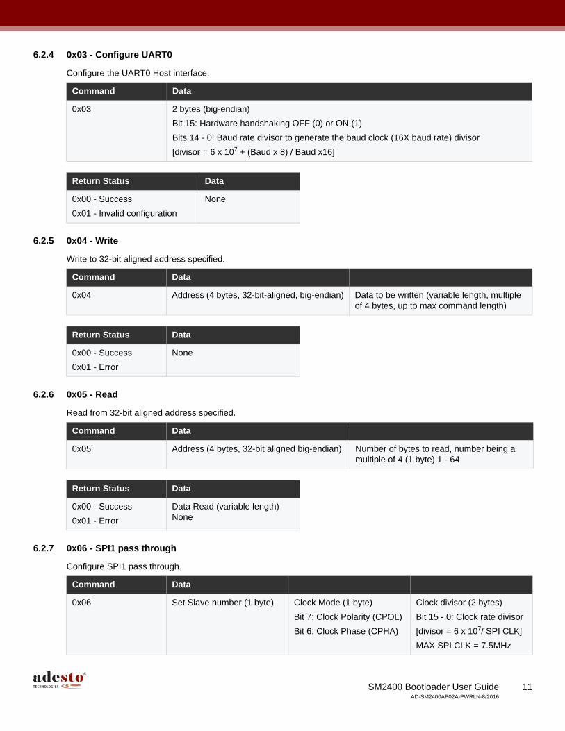
7. Code examples
This section contains code examples that may be useful in communicating with the bootloader.
7.1 32-BIT CRC example (implemented in C)
// polynomial: 0x104C11DB7static uint32_t crc32_table[] = { 0x00000000, 0x1db71064, 0x3b6e20c8, 0x26d930ac, 0x76dc4190, 0x6b6b51f4, 0x4db26158, 0x5005713c, 0xedb88320, 0xf00f9344, 0xd6d6a3e8, 0xcb61b38c, 0x9b64c2b0, 0x86d3d2d4, 0xa00ae278, 0xbdbdf21c};
// CRC calculationuint32_t crc32_calc(uint32_t crc, uint8_t *data, uint32_t ix, uint32_t len){ uint32_t k, m, d;
for (k = 0; k < len; k++) { d = (uint32_t)data[ix + k] ^ crc; m = crc32_table[d & 0x0f];
d >>= 4; d ^= m;
crc >>= 8; crc ^= m >> 4; crc ^= crc32_table[d & 0x0f]; } return crc;}
7.2 Bootloader command transmit example (implemented in C)
uint32_t ccitt_crc16_table[] = { 0x0000, 0x1021, 0x2042, 0x3063, 0x4084, 0x50a5, 0x60c6, 0x70e7, 0x8108, 0x9129, 0xa14a, 0xb16b, 0xc18c, 0xd1ad, 0xe1ce, 0xf1ef, 0x1231, 0x0210, 0x3273, 0x2252, 0x52b5, 0x4294, 0x72f7, 0x62d6, 0x9339, 0x8318, 0xb37b, 0xa35a, 0xd3bd, 0xc39c, 0xf3ff, 0xe3de, 0x2462, 0x3443, 0x0420, 0x1401, 0x64e6, 0x74c7, 0x44a4, 0x5485, 0xa56a, 0xb54b, 0x8528, 0x9509, 0xe5ee, 0xf5cf, 0xc5ac, 0xd58d, 0x3653, 0x2672, 0x1611, 0x0630, 0x76d7, 0x66f6, 0x5695, 0x46b4, 0xb75b, 0xa77a, 0x9719, 0x8738, 0xf7df, 0xe7fe, 0xd79d, 0xc7bc, 0x48c4, 0x58e5, 0x6886, 0x78a7, 0x0840, 0x1861, 0x2802, 0x3823, 0xc9cc, 0xd9ed, 0xe98e, 0xf9af, 0x8948, 0x9969, 0xa90a, 0xb92b, 0x5af5, 0x4ad4, 0x7ab7, 0x6a96, 0x1a71, 0x0a50, 0x3a33, 0x2a12, 0xdbfd, 0xcbdc, 0xfbbf, 0xeb9e, 0x9b79, 0x8b58, 0xbb3b, 0xab1a, 0x6ca6, 0x7c87, 0x4ce4, 0x5cc5, 0x2c22, 0x3c03, 0x0c60, 0x1c41, 0xedae, 0xfd8f, 0xcdec, 0xddcd, 0xad2a, 0xbd0b, 0x8d68, 0x9d49,
14SM2400 Bootloader User Guide AD-SM2400AP02A-PWRLN-8/2016

0x7e97, 0x6eb6, 0x5ed5, 0x4ef4, 0x3e13, 0x2e32, 0x1e51, 0x0e70, 0xff9f, 0xefbe, 0xdfdd, 0xcffc, 0xbf1b, 0xaf3a, 0x9f59, 0x8f78, 0x9188, 0x81a9, 0xb1ca, 0xa1eb, 0xd10c, 0xc12d, 0xf14e, 0xe16f, 0x1080, 0x00a1, 0x30c2, 0x20e3, 0x5004, 0x4025, 0x7046, 0x6067, 0x83b9, 0x9398, 0xa3fb, 0xb3da, 0xc33d, 0xd31c, 0xe37f, 0xf35e, 0x02b1, 0x1290, 0x22f3, 0x32d2, 0x4235, 0x5214, 0x6277, 0x7256, 0xb5ea, 0xa5cb, 0x95a8, 0x8589, 0xf56e, 0xe54f, 0xd52c, 0xc50d, 0x34e2, 0x24c3, 0x14a0, 0x0481, 0x7466, 0x6447, 0x5424, 0x4405, 0xa7db, 0xb7fa, 0x8799, 0x97b8, 0xe75f, 0xf77e, 0xc71d, 0xd73c, 0x26d3, 0x36f2, 0x0691, 0x16b0, 0x6657, 0x7676, 0x4615, 0x5634, 0xd94c, 0xc96d, 0xf90e, 0xe92f, 0x99c8, 0x89e9, 0xb98a, 0xa9ab, 0x5844, 0x4865, 0x7806, 0x6827, 0x18c0, 0x08e1, 0x3882, 0x28a3, 0xcb7d, 0xdb5c, 0xeb3f, 0xfb1e, 0x8bf9, 0x9bd8, 0xabbb, 0xbb9a, 0x4a75, 0x5a54, 0x6a37, 0x7a16, 0x0af1, 0x1ad0, 0x2ab3, 0x3a92, 0xfd2e, 0xed0f, 0xdd6c, 0xcd4d, 0xbdaa, 0xad8b, 0x9de8, 0x8dc9, 0x7c26, 0x6c07, 0x5c64, 0x4c45, 0x3ca2, 0x2c83, 0x1ce0, 0x0cc1, 0xef1f, 0xff3e, 0xcf5d, 0xdf7c, 0xaf9b, 0xbfba, 0x8fd9, 0x9ff8, 0x6e17, 0x7e36, 0x4e55, 0x5e74, 0x2e93, 0x3eb2, 0x0ed1, 0x1ef0};
int32_t add_byte(uint8_t *buf, int32_t *k, int32_t *crc, uint8_t byt){ int32_t nb = 1; buf[(*k)++] = byt; if (byt == BL_ESC) { buf[(*k)++] = BL_IESC; nb = 2; } *crc = ccitt_crc16_table[((*crc) >> 8 ^ (uint32_t)byt) & 0xff] ^ ((*crc) << 8); return nb;}
// Encode bootloader packetint32_t bl_encode(uint8_t *buf, uint8_t *inp, int32_t len, uint8_t cmd){ int32_t i, k, crc, dcrc;
crc = 0; k = 0; buf[k++] = BL_ESC; buf[k++] = BL_ESC2; add_byte(buf, &k, &crc, cmd); add_byte(buf, &k, &crc, len);
for (i = 0; i < len; i++) add_byte(buf, &k, &crc, inp[i]); dcrc = 0; add_byte(buf, &k, &dcrc, (uint8_t)(crc >> 8)); add_byte(buf, &k, &dcrc, (uint8_t)(crc >> 0)); return k;}
// Decode response from SPI - removing escape sequences and checking CRC
15SM2400 Bootloader User Guide AD-SM2400AP02A-PWRLN-8/2016
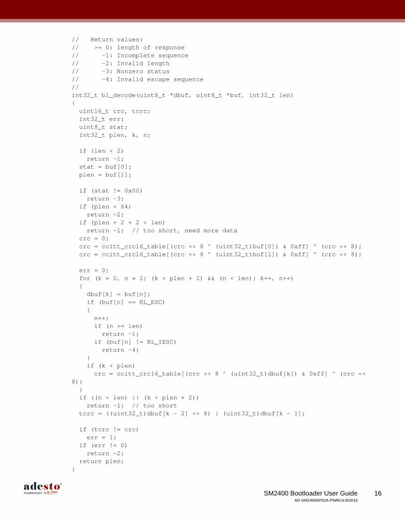
// Return values:// >= 0: length of response// -1: Incomplete sequence// -2: Invalid length// -3: Nonzero status// -4: Invalid escape sequence//int32_t bl_decode(uint8_t *dbuf, uint8_t *buf, int32_t len){ uint16_t crc, tcrc; int32_t err; uint8_t stat; int32_t plen, k, n;
if (len < 2) return -1; stat = buf[0]; plen = buf[1];
if (stat != 0x00) return -3; if (plen > 64) return -2; if (plen + 2 + 2 > len) return -1; // too short, need more data crc = 0; crc = ccitt_crc16_table[(crc >> 8 ^ (uint32_t)buf[0]) & 0xff] ^ (crc << 8); crc = ccitt_crc16_table[(crc >> 8 ^ (uint32_t)buf[1]) & 0xff] ^ (crc << 8);
err = 0; for (k = 0, n = 2; (k < plen + 2) && (n < len); k++, n++) { dbuf[k] = buf[n]; if (buf[n] == BL_ESC) { n++; if (n >= len) return -1; if (buf[n] != BL_IESC) return -4; } if (k < plen) crc = ccitt_crc16_table[(crc >> 8 ^ (uint32_t)dbuf[k]) & 0xff] ^ (crc << 8); } if ((n < len) || (k < plen + 2)) return -1; // too short tcrc = ((uint32_t)dbuf[k - 2] << 8) | (uint32_t)dbuf[k - 1];
if (tcrc != crc) err = 1; if (err != 0) return -2; return plen;}
16SM2400 Bootloader User Guide AD-SM2400AP02A-PWRLN-8/2016

// Read bootloader UARTint32_t bl_read(void *serialHandle, uint8_t *decbuf, int32_t maxlen){ int32_t k, res;
k = uart_read(serialHandle, rxbuf + rbp, BLRXBUF_SIZE - rbp); if (k == 0) return -1; rbp += k; res = bl_decode(decbuf, rxbuf, rbp);
if ((res == -1) || (res == -4)) // too short, will come back here return -1; rbp = 0; if ((res == -2) || (res == -3)) // outright error return -2; return res;}
// Send a command to SPIint32_t sendHostCommand(void *serialHandle, uint8_t *response, int32_t maxrlen, uint8_t *request, int32_t len, uint8_t command){ int32_t elen, rlen; int32_t timeout; uint8_t pkt[160];
elen = bl_encode(pkt, request, len, command); uart_write(serialHandle, pkt, elen);
timeout = 100; while (timeout-- > 0) { rlen = bl_read(serialHandle, response, maxrlen); if (rlen >= 0) return rlen; sleep(10); } return -1; // timeout}
17SM2400 Bootloader User Guide AD-SM2400AP02A-PWRLN-8/2016
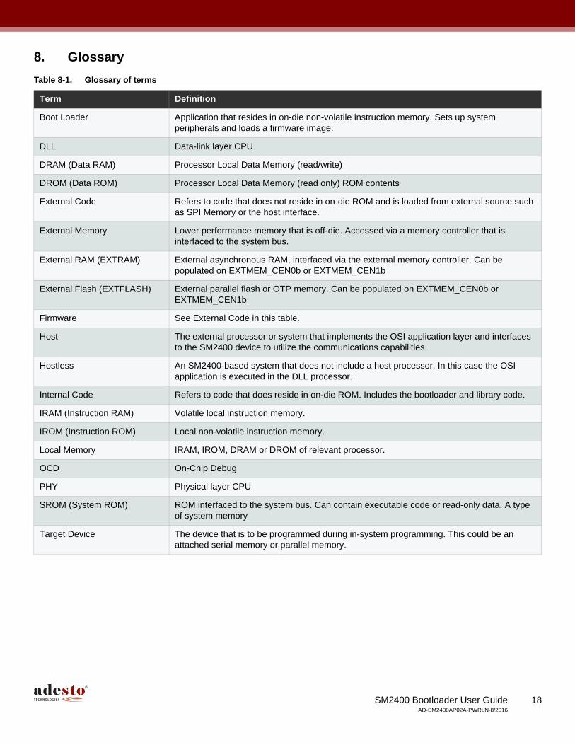
8. Glossary
Table 8-1. Glossary of terms
Term Definition
Boot Loader Application that resides in on-die non-volatile instruction memory. Sets up system peripherals and loads a firmware image.
DLL Data-link layer CPU
DRAM (Data RAM) Processor Local Data Memory (read/write)
DROM (Data ROM) Processor Local Data Memory (read only) ROM contents
External Code Refers to code that does not reside in on-die ROM and is loaded from external source such as SPI Memory or the host interface.
External Memory Lower performance memory that is off-die. Accessed via a memory controller that is interfaced to the system bus.
External RAM (EXTRAM) External asynchronous RAM, interfaced via the external memory controller. Can be populated on EXTMEM_CEN0b or EXTMEM_CEN1b
External Flash (EXTFLASH) External parallel flash or OTP memory. Can be populated on EXTMEM_CEN0b or EXTMEM_CEN1b
Firmware See External Code in this table.
Host The external processor or system that implements the OSI application layer and interfaces to the SM2400 device to utilize the communications capabilities.
Hostless An SM2400-based system that does not include a host processor. In this case the OSI application is executed in the DLL processor.
Internal Code Refers to code that does reside in on-die ROM. Includes the bootloader and library code.
IRAM (Instruction RAM) Volatile local instruction memory.
IROM (Instruction ROM) Local non-volatile instruction memory.
Local Memory IRAM, IROM, DRAM or DROM of relevant processor.
OCD On-Chip Debug
PHY Physical layer CPU
SROM (System ROM) ROM interfaced to the system bus. Can contain executable code or read-only data. A type of system memory
Target Device The device that is to be programmed during in-system programming. This could be an attached serial memory or parallel memory.
18SM2400 Bootloader User Guide AD-SM2400AP02A-PWRLN-8/2016
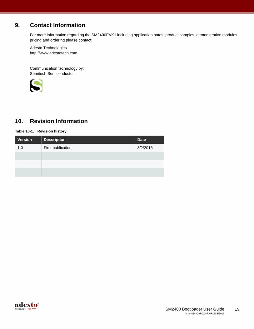
9. Contact Information
For more information regarding the SM2400EVK1 including application notes, product samples, demonstration modules, pricing and ordering please contact:
Adesto Technologieshttp://www.adestotech.com
Communication technology by:Semitech Semiconductor
10. Revision Information
Table 10-1. Revision history
Version Description Date
1.0 First publication 8/2/2016
19SM2400 Bootloader User Guide AD-SM2400AP02A-PWRLN-8/2016

Corporate Office
©2016 Adesto Technologies. All rights reserved. / Rev.: PB2480A–PWRLN–5/2016
Disclaimer: Adesto Technologies Corporation makes no warranty for the use of its products, other than those expressly contained in the Company's standard warranty which is detailed in Adesto's Terms and Conditions located on the Company's web site. The Company assumes no responsibility for any errors which may appear in this document, reserves the right to change devices or specifications detailed herein at any time without notice, and does not make any commitment to update the information contained herein. No licenses to patents or other intellectual property of Adesto are granted by the Company in connection with the sale of Adesto products, expressly or by implication. Adesto's products are not authorized for use as critical components in life support devices or systems.
California | USA
Adesto Headquarters
3600 Peterson WaySanta Clara, CA 95054Phone: (+1) 408.400.0578
Email: [email protected]