SLLSEV1A –SEPTEMBER 2017–REVISED JANUARY … · Bus terminals and GND ±30,000 All pins except...
41
B A (9 ) 12 (8 ) 11 R D 2 (1) 5 (4) RE DE 3 (2) 4 (3) Y Z (7 ) 10 (6) 9 Copyright © 2017, Texas Instruments Incorporated B A Y Z R D 2 3 8 7 6 5 Copyright © 2017, Texas Instruments Incorporated A B 7 6 R D 1 4 RE DE 2 3 Copyright © 2017, Texas Instruments Incorporated Product Folder Order Now Technical Documents Tools & Software Support & Community An IMPORTANT NOTICE at the end of this data sheet addresses availability, warranty, changes, use in safety-critical applications, intellectual property matters and other important disclaimers. PRODUCTION DATA. THVD1510, THVD1512 THVD1550, THVD1551, THVD1552 SLLSEV1A – SEPTEMBER 2017 – REVISED JANUARY 2018 THVD15xx 5-V RS-485 Transceivers With ±18-kV IEC ESD Protection 1 1 Features 1• Meets or Exceeds the Requirements of the TIA/EIA-485A Standard • 4.5 V to 5.5 V Supply Voltage • Integrated Bus I/O Protection – ± 30 kV HBM ESD – ± 18 kV IEC 61000-4-2 ESD Contact Discharge – ± 25 kV IEC 61000-4-2 ESD Air-Gap Discharge – ± 4 kV IEC 61000-4-4 Electrical Fast Transient • Extended Operational Common-mode: ± 15 V • Low EMI 500 kbps and 50 Mbps Data Rates • Extended Temperature Range: -40°C to 125°C • Large Receiver Hysteresis for Noise Rejection • Low Power Consumption – Low Standby Supply Current: < 1 μA – Current During Operation: < 1 mA • Glitch-Free Power-Up/Down for Hot Plug-in Capability • Open, Short, and Idle Bus Failsafe • 1/8 Unit Load Options (Up to 256 Bus Nodes) • Small-Size VSSOP Packages Save Board Space or SOIC for Drop-in Compatibility 2 Applications • Motor Drives • Factory Automation and Control • Grid Infrastructure • Building Automation • HVAC Systems • Video Surveillance • Process Analytics • Telecom Infrastructure 3 Description THVD15xx is a family of noise-immune RS-485/RS- 422 transceivers designed to operate in rugged industrial environments. The bus pins of these devices are robust to high levels of IEC electrical fast transients (EFT) and IEC electrostatic discharge (ESD) events, eliminating the need for additional system-level protection components. Each of these devices operates from a single 5-V supply. The devices in this family feature an extended common-mode voltage range which makes them suitable for multi-point applications over long cable runs. THVD15xx family of devices is available in small VSSOP packages for space-constrained applications. These devices are characterized over ambient free- air temperatures from –40°C to 125°C. Device Information (1) PART NUMBER PACKAGE BODY SIZE (NOM) THVD1510 THVD1550 VSSOP (8) 3.00 mm × 3.00 mm SOIC (8) 4.90 mm × 3.91 mm THVD1551 VSSOP (8) 3.00 mm × 3.00 mm THVD1512 VSSOP (10) 3.00 mm × 3.00 mm THVD1552 VSSOP (10) 3.00 mm × 3.00 mm SOIC (14) 8.65 mm × 3.91 mm (1) For all available packages, see the orderable addendum at the end of the data sheet. THVD1510 and THVD1550 Simplified Schematic THVD1551 Simplified Schematic THVD1512 and THVD1552 Simplified Schematic
Transcript of SLLSEV1A –SEPTEMBER 2017–REVISED JANUARY … · Bus terminals and GND ±30,000 All pins except...

B
A(9 ) 12
(8 ) 11R
D
2 (1)
5 (4)
RE
DE
3 (2)
4 (3)
Y
Z(7 ) 10
(6) 9
Copyright © 2017, Texas Instruments Incorporated
B
A
Y
Z
R
D
2
3
8
7
6
5
Copyright © 2017, Texas Instruments Incorporated
A
B7
6
R
D
1
4
RE
DE
2
3
Copyright © 2017, Texas Instruments Incorporated
Product
Folder
Order
Now
Technical
Documents
Tools &
Software
Support &Community
An IMPORTANT NOTICE at the end of this data sheet addresses availability, warranty, changes, use in safety-critical applications,intellectual property matters and other important disclaimers. PRODUCTION DATA.
THVD1510, THVD1512THVD1550, THVD1551, THVD1552
SLLSEV1A –SEPTEMBER 2017–REVISED JANUARY 2018
THVD15xx 5-V RS-485 Transceivers With ±18-kV IEC ESD Protection
1
1 Features1• Meets or Exceeds the Requirements of the
TIA/EIA-485A Standard• 4.5 V to 5.5 V Supply Voltage• Integrated Bus I/O Protection
– ± 30 kV HBM ESD– ± 18 kV IEC 61000-4-2 ESD Contact
Discharge– ± 25 kV IEC 61000-4-2 ESD Air-Gap
Discharge– ± 4 kV IEC 61000-4-4 Electrical Fast Transient
• Extended Operational Common-mode: ± 15 V• Low EMI 500 kbps and 50 Mbps Data Rates• Extended Temperature Range: -40°C to 125°C• Large Receiver Hysteresis for Noise Rejection• Low Power Consumption
– Low Standby Supply Current: < 1 µA– Current During Operation: < 1 mA
• Glitch-Free Power-Up/Down for Hot Plug-inCapability
• Open, Short, and Idle Bus Failsafe• 1/8 Unit Load Options (Up to 256 Bus Nodes)• Small-Size VSSOP Packages Save Board Space
or SOIC for Drop-in Compatibility
2 Applications• Motor Drives• Factory Automation and Control• Grid Infrastructure• Building Automation• HVAC Systems• Video Surveillance• Process Analytics• Telecom Infrastructure
3 DescriptionTHVD15xx is a family of noise-immune RS-485/RS-422 transceivers designed to operate in ruggedindustrial environments. The bus pins of thesedevices are robust to high levels of IEC electrical fasttransients (EFT) and IEC electrostatic discharge(ESD) events, eliminating the need for additionalsystem-level protection components.
Each of these devices operates from a single 5-Vsupply. The devices in this family feature an extendedcommon-mode voltage range which makes themsuitable for multi-point applications over long cableruns.
THVD15xx family of devices is available in smallVSSOP packages for space-constrained applications.These devices are characterized over ambient free-air temperatures from –40°C to 125°C.
Device Information(1)
PART NUMBER PACKAGE BODY SIZE (NOM)
THVD1510THVD1550
VSSOP (8) 3.00 mm × 3.00 mmSOIC (8) 4.90 mm × 3.91 mm
THVD1551 VSSOP (8) 3.00 mm × 3.00 mmTHVD1512 VSSOP (10) 3.00 mm × 3.00 mm
THVD1552VSSOP (10) 3.00 mm × 3.00 mmSOIC (14) 8.65 mm × 3.91 mm
(1) For all available packages, see the orderable addendum atthe end of the data sheet.
THVD1510 and THVD1550 Simplified Schematic
THVD1551 Simplified Schematic
THVD1512 and THVD1552 Simplified Schematic

2
THVD1510, THVD1512THVD1550, THVD1551, THVD1552SLLSEV1A –SEPTEMBER 2017–REVISED JANUARY 2018 www.ti.com
Product Folder Links: THVD1510 THVD1512 THVD1550 THVD1551 THVD1552
Submit Documentation Feedback Copyright © 2017–2018, Texas Instruments Incorporated
Table of Contents1 Features .................................................................. 12 Applications ........................................................... 13 Description ............................................................. 14 Revision History..................................................... 25 Device Comparison Table ..................................... 36 Pin Configuration and Functions ......................... 37 Specifications......................................................... 6
7.1 Absolute Maximum Ratings ...................................... 67.2 ESD Ratings ............................................................ 67.3 Recommended Operating Conditions....................... 77.4 Thermal Information .................................................. 77.5 Power Dissipation ..................................................... 77.6 Electrical Characteristics........................................... 87.7 Switching Characteristics .......................................... 97.8 Switching Characteristics .......................................... 97.9 Typical Characteristics ............................................ 10
8 Parameter Measurement Information ................ 119 Detailed Description ............................................ 14
9.1 Overview ................................................................. 149.2 Functional Block Diagrams ..................................... 14
9.3 Feature Description................................................. 159.4 Device Functional Modes........................................ 15
10 Application and Implementation........................ 1810.1 Application Information...................................... 1810.2 Typical Application ............................................... 18
11 Power Supply Recommendations ..................... 2412 Layout................................................................... 25
12.1 Layout Guidelines ................................................. 2512.2 Layout Example .................................................... 25
13 Device and Documentation Support ................. 2613.1 Device Support...................................................... 2613.2 Third-Party Products Disclaimer ........................... 2613.3 Related Links ........................................................ 2613.4 Receiving Notification of Documentation Updates 2613.5 Community Resources.......................................... 2613.6 Trademarks ........................................................... 2613.7 Electrostatic Discharge Caution............................ 2613.8 Glossary ................................................................ 26
14 Mechanical, Packaging, and OrderableInformation ........................................................... 27
4 Revision History
Changes from Original (September 2017) to Revision A Page
• Changed the Machine model (MM) value From: ±400 To: ±200 in the ESD Ratings ............................................................ 6• Changed the VOH MIN value From: 2.4 V To: 4 V in the Electrical Characteristics table ..................................................... 8

Not to scale
1R 8 VCC
2/RE 7 B
3DE 6 A
4D 5 GND
Not to scale
1R 8 VCC
2/RE 7 B
3DE 6 A
4D 5 GND
3
THVD1510, THVD1512THVD1550, THVD1551, THVD1552
www.ti.com SLLSEV1A –SEPTEMBER 2017–REVISED JANUARY 2018
Product Folder Links: THVD1510 THVD1512 THVD1550 THVD1551 THVD1552
Submit Documentation FeedbackCopyright © 2017–2018, Texas Instruments Incorporated
5 Device Comparison Table
PART NUMBER DUPLEX ENABLES SIGNALING RATE NODESTHVD1512 Full DE, RE
up to 500 kbps 256THVD1510 Half DE, RETHVD1552 Full DE, RE
up to 50 Mbps 196THVD1551 Full NoneTHVD1550 Half DE, RE
6 Pin Configuration and Functions
THVD1510, THVD1550 Devices8-Pin D Package (SOIC)
Top ViewTHVD1510, THVD1550 Devices8-Pin DGK Package (VSSOP)
Top View
Pin FunctionsPIN
I/O DESCRIPTIONNAME D DGKA 6 6 Bus input/output Bus I/O port, A (complementary to B)B 7 7 Bus input/output Bus I/O port, B (complementary to A)D 4 4 Digital input Driver data inputDE 3 3 Digital input Driver enable, active high (2 MΩ internal pull-down)GND 5 5 Ground Device groundR 1 1 Digital output Receive data outputVCC 8 8 Power 5-V supplyRE 2 2 Digital input Receiver enable, active low (2 MΩ internal pull-up)

Not to scale
1VCC 8 A
2R 7 B
3D 6 Z
4GND 5 Y
4
THVD1510, THVD1512THVD1550, THVD1551, THVD1552SLLSEV1A –SEPTEMBER 2017–REVISED JANUARY 2018 www.ti.com
Product Folder Links: THVD1510 THVD1512 THVD1550 THVD1551 THVD1552
Submit Documentation Feedback Copyright © 2017–2018, Texas Instruments Incorporated
THVD1551 Device8-Pin DGK Package (VSSOP)
Top View
Pin FunctionsPIN
I/O DESCRIPTIONNAME DGKA 8 Bus input Bus input, A (complementary to B)B 7 Bus input Bus input, B (complementary to A)D 3 Digital input Driver data inputGND 4 Ground Device groundR 2 Digital output Receive data outputVCC 1 Power 5-V supplyY 5 Bus output Bus output, Y (complementary to Z)Z 6 Bus output Bus output, Z (complementary to Y)

Not to scale
1NC 14 VCC
2R 13 VCC
3/RE 12 A
4DE 11 B
5D 10 Z
6GND 9 Y
7GND 8 NC
Not to scale
1R 10 VCC
2RE 9 A
3DE 8 B
4D 7 Z
5GND 6 Y
5
THVD1510, THVD1512THVD1550, THVD1551, THVD1552
www.ti.com SLLSEV1A –SEPTEMBER 2017–REVISED JANUARY 2018
Product Folder Links: THVD1510 THVD1512 THVD1550 THVD1551 THVD1552
Submit Documentation FeedbackCopyright © 2017–2018, Texas Instruments Incorporated
THVD1552 Device14-Pin D Package (SOIC)
Top ViewTHVD1512, THVD1552 Devices10-Pin DGS Package (VSSOP)
Top View
(1) These pins are internally connected
Pin FunctionsPIN
I/O DESCRIPTIONNAME D DGSA 12 9 Bus input Bus input, A (complementary to B)B 11 8 Bus input Bus input, B (complementary to A)D 5 4 Digital input Driver data inputDE 4 3 Digital input Driver enable, active high (2 MΩ internal pull-down)GND 6, 7 (1) 5 Ground Device groundNC 1, 8 — — Internally not connectedR 2 1 Digital output Receive data outputVCC 13, 14 (1) 10 Power 5-V supplyY 9 6 Bus output Bus output, Y (Complementary to Z)Z 10 7 Bus output Bus output, Z (Complementary to Y)RE 3 2 Digital input Receiver enable, active low (2 MΩ internal pull-up)

6
THVD1510, THVD1512THVD1550, THVD1551, THVD1552SLLSEV1A –SEPTEMBER 2017–REVISED JANUARY 2018 www.ti.com
Product Folder Links: THVD1510 THVD1512 THVD1550 THVD1551 THVD1552
Submit Documentation Feedback Copyright © 2017–2018, Texas Instruments Incorporated
(1) Stresses beyond those listed under Absolute Maximum Ratings may cause permanent damage to the device. These are stress ratingsonly, which do not imply functional operation of the device at these or any other conditions beyond those indicated under RecommendedOperating Conditions. Exposure to absolute-maximum-rated conditions for extended periods may affect device reliability.
7 Specifications
7.1 Absolute Maximum Ratingsover operating free-air temperature range (unless otherwise noted) (1)
MIN MAX UNITSupply voltage VCC –0.5 7 V
Bus voltageRange at any bus pin (A, B, Y, or Z) asdifferential or common-mode with respect toGND
–18 18 V
Input voltage Range at any logic pin (D, DE, or RE) –0.3 5.7 VReceiver output current IO –24 24 mAStorage temperature, Tstg –65 150 °C
(1) JEDEC document JEP155 states that 500-V HBM allows safe manufacturing with a standard ESD control process.(2) JEDEC document JEP157 states that 250-V CDM allows safe manufacturing with a standard ESD control process.
7.2 ESD RatingsVALUE UNIT
V(ESD) Electrostatic discharge
Contact discharge, per IEC 61000-4-2 Bus terminals and GND ±18,000
V
Air-gap discharge, per IEC 61000-4-2 Bus terminals and GND ±25,000
Human-body model (HBM), perANSI/ESDA/JEDEC JS-001 (1)
Bus terminals and GND ±30,000All pins except Busterminals and GND ±8,000
Charged-device model (CDM), per JEDEC specification JESD22-C101 (2) ±1,500
Machine model (MM), per JEDEC JESD22-A115-A ±200V(EFT) Electrical fast transient Per IEC 61000-4-4 Bus terminals ±4,000 V

7
THVD1510, THVD1512THVD1550, THVD1551, THVD1552
www.ti.com SLLSEV1A –SEPTEMBER 2017–REVISED JANUARY 2018
Product Folder Links: THVD1510 THVD1512 THVD1550 THVD1551 THVD1552
Submit Documentation FeedbackCopyright © 2017–2018, Texas Instruments Incorporated
(1) The algebraic convention, in which the least positive (most negative) limit is designated as minimum is used in this data sheet.
7.3 Recommended Operating Conditionsover operating free-air temperature range (unless otherwise noted)
MIN NOM MAX UNITVCC Supply voltage 4.5 5.5 VVI Input voltage at any bus terminal (1) -15 15 V
VIHHigh-level input voltage (driver, driver enable, and receiver enableinputs) 2 VCC V
VILLow-level input voltage (driver, driver enable, and receiver enableinputs) 0 0.8 V
VID Differential input voltage -15 15 VIO Output current, driver -60 60 mAIOR Output current, receiver -8 8 mARL Differential load resistance 54 Ω
1/tUI Signaling rateTHVD1510, THVD1512 500 kbpsTHVD1550, THVD1551, THVD1552 50 Mbps
TA Operating ambient temperature -40 125 °CTJ Junction temperature -40 150 °C
(1) For more information about traditional and new thermal metrics, see the Semiconductor and IC Package Thermal Metrics applicationreport.
7.4 Thermal Information
THERMAL METRIC (1)
THVD1510THVD1550 THVD1552
THVD1510THVD1550THVD1551
THVD1512THVD1552
UNITD (SOIC) D (SOIC) DGK (VSSOP) DGS (VSSOP)8 PINS 14 PINS 8 PINS 10 PINS
RθJA Junction-to-ambient thermal resistance 112.4 88.0 151.7 151.4 °C/WRθJC(top) Junction-to-case (top) thermal resistance 62.7 45.4 62.8 59.3 °C/WRθJB Junction-to-board thermal resistance 62.0 44.1 81.3 81.6 °C/WψJT Junction-to-top characterization parameter 15.4 11.3 7.8 6.5 °C/WψJB Junction-to-board characterization parameter 61.3 43.7 79.8 79.9 °C/WRθJC(bot) Junction-to-case (bottom) thermal resistance N/A N/A N/A N/A °C/W
7.5 Power DissipationPARAMETER TEST CONDITIONS VALUE UNIT
PD
Driver and receiver enabled,VCC = 5.5 V, TA = 125 °C,50% duty cycle square wave atsignaling rate
UnterminatedRL = 300 Ω, CL = 50 pF (driver)
THVD151x 500 kbps 210mW
THVD155x 50 Mbps 350
RS-422 loadRL = 100 Ω, CL = 50 pF (driver)
THVD151x 500 kbps 220mW
THVD155x 50 Mbps 330
RS-485 loadRL = 54 Ω, CL = 50 pF (driver)
THVD151x 500 kbps 250mW
THVD155x 50 Mbps 340

8
THVD1510, THVD1512THVD1550, THVD1551, THVD1552SLLSEV1A –SEPTEMBER 2017–REVISED JANUARY 2018 www.ti.com
Product Folder Links: THVD1510 THVD1512 THVD1550 THVD1551 THVD1552
Submit Documentation Feedback Copyright © 2017–2018, Texas Instruments Incorporated
(1) Under any specific conditions, VTH+ is specified to be at least VHYS higher than VTH–.
7.6 Electrical Characteristicsover operating free-air temperature range (unless otherwise noted)
PARAMETER TEST CONDITIONS MIN TYP MAX UNIT
Driver
|VOD| Driver differential outputvoltage magnitude
RL = 60 Ω, -15 V ≤ Vtest ≤ 15 V, (See Figure 11) 1.5 2.7 V
RL = 100 Ω (See Figure 12) 2 3 V
RL = 54 Ω (See Figure 12) 1.5 2.7 V
Δ|VOD| Change in differential outputvoltage
RL = 54 Ω (See Figure 12)
–200 200 mV
VOCCommon-mode outputvoltage 1 VCC/2 3 V
ΔVOC(SS)
Change in steady-statecommon-mode outputvoltage
–200 200 mV
IOS Short-circuit output current DE = VCC, -15 V ≤ VO ≤ 15V –250 250 mA
Receiver
II Bus input current DE = 0 V, VCC = 0 V or 5.5 V
THVD151x
VI = 12 V 75 125
μA
VI = 15 V 95 156
VI = -7 V -100 -40
VI = -15 V -215 -85
THVD155x
VI = 12 V 115 160
VI = 15 V 150 200
VI = -7 V -130 -75
VI = -15 V -280 -180
Receiver
VTH+Positive-going inputthreshold voltage
Over common-mode range of - 7 V to +12 V
See (1) –85 –20 mV
VTH-Negative-going inputthreshold voltage –200 –135 See (1) mV
VHYS Input hysteresis 50 mV
VTH+Positive-going inputthreshold voltage
Over common-mode range of ± 15 V
See (1) –85 –20 mV
VTH-Negative-going inputthreshold voltage –220 –135 See (1) mV
VHYS Input hysteresis 50 mV
VOH Output high voltage IOH = -8 mA 4 VCC - 0.3 V
VOL Output low voltage IOL = 8 mA 0.2 0.4 V
IOZOutput high-impedancecurrent VO = 0 V or VCC, RE = VCC -1 1 µA
Logic
IIN Input current (D, DE, RE) 4.5 V ≤ VCC ≤ 5.5 V, 0 V ≤ VIN ≤ VCC –5 0 5 µA
Supply
ICC Supply current (quiescent)
Driver and receiver enabled RE = 0 V, DE = VCC,No load 700 1000 µA
Driver enabled, receiver disabled RE = VCC, DE = VCC,No load 400 620 µA
Driver disabled, receiver enabled RE = 0 V, DE = 0 V,No load 400 630 µA
Driver and receiver disabled RE = VCC, DE = 0 V,D = open, No load 0.1 1 µA

9
THVD1510, THVD1512THVD1550, THVD1551, THVD1552
www.ti.com SLLSEV1A –SEPTEMBER 2017–REVISED JANUARY 2018
Product Folder Links: THVD1510 THVD1512 THVD1550 THVD1551 THVD1552
Submit Documentation FeedbackCopyright © 2017–2018, Texas Instruments Incorporated
7.7 Switching Characteristics500-kbps devices (THVD1510, THVD1512) over recommended operating conditions
PARAMETER TEST CONDITIONS MIN TYP MAX UNIT
Driver
tr, tf Differential output rise/fall time
RL = 54 Ω, CL = 50 pF See Figure 13
300 400 600 ns
tPHL, tPLH Propagation delay 350 500 ns
tSK(P) Pulse skew, |tPHL – tPLH| 15 ns
tPHZ, tPLZDisable time (THVD1510,THVD1512) See Figure 14 and
Figure 15
110 200 ns
tPZH, tPZLEnable time (THVD1510,THVD1512)
RE = 0 V 100 500 ns
RE = VCC 2 4 µs
Receiver
tr, tf Differential output rise/fall time
CL = 15 pF See Figure 16
15 25 ns
tPHL, tPLH Propagation delay 50 60 ns
tSK(P) Pulse skew, |tPHL – tPLH| 10 ns
tPHZ, tPLZDisable time (THVD1510,THVD1512) 30 40 ns
tPZH(1),tPZL(1),tPZH(2),tPZL(2)
Enable time (THVD1510,THVD1512)
DE = VCC See Figure 17 60 100 ns
DE = 0 V See Figure 18 3 8 μs
7.8 Switching Characteristics50-Mbps devices (THVD1550, THVD1551, THVD1552) over recommended operating conditions
PARAMETER TEST CONDITIONS MIN TYP MAX UNIT
Driver
tr, tf Differential output rise/fall time
RL = 54 Ω, CL = 50 pF See Figure 13
1 2 6 ns
tPHL, tPLH Propagation delay 5 10 16 ns
tSK(P) Pulse skew, |tPHL – tPLH| 3.5 ns
tPHZ, tPLZDisable time (THVD1550,THVD1552) See Figure 14 and
Figure 15
10 22 ns
tPZH, tPZLEnable time (THVD1550,THVD1552)
RE = 0 V 10 22 ns
RE = VCC 2 4 μs
Receiver
tr, tf Differential output rise/fall time
CL = 15 pF See Figure 16
1 3 6 ns
tPHL, tPLH Propagation delay 30 45 ns
tSK(P) Pulse skew, |tPHL – tPLH| 2 ns
tPHZ, tPLZDisable time (THVD1550,THVD1552) 8 18 ns
tPZH(1),tPZL(1),tPZH(2),tPZL(2)
Enable time (THVD1550,THVD1552)
DE = VCC See Figure 17 55 90 ns
DE = 0 V See Figure 18 3 8 μs

Temperature (qC)
VO
- D
river
Pro
paga
tion
Del
ay (
ns)
-40 -20 0 20 40 60 80 100 120 140330
335
340
345
350
355
360
365
370
375
380
385
390
395
D005 Temperature (qC)
VO
- D
river
Ris
e an
d F
all T
ime
(ns)
-40 -20 0 20 40 60 80 100 1200
0.5
1
1.5
2
2.5
3
D006
VCC - Supply Voltage (V)
I O -
Driv
er O
utpu
t Cur
rent
(m
A)
0 0.5 1 1.5 2 2.5 3 3.5 4 4.5 5 5.5 60
10
20
30
40
50
60
D003 Temperature (qC)
V0
- D
river
Ris
e an
d F
all T
ime
(ns)
-40 -20 0 20 40 60 80 100 120380
390
400
410
420
430
440
450
460
D004
IO - Driver Output Current (mA)
VO
- D
river
Out
put V
olta
ge (
V)
0 10 20 30 40 50 60 70 80 90 100 1100
0.5
1
1.5
2
2.5
3
3.5
4
4.5
5
D001
VOLVOH
IO - Driver Output Current (mA)
VO
- D
river
Diff
eren
tial O
utpu
t Vol
tage
(V
)
0 10 20 30 40 50 60 70 80 90 100 1100
0.5
1
1.5
2
2.5
3
3.5
4
4.5
D002
10
THVD1510, THVD1512THVD1550, THVD1551, THVD1552SLLSEV1A –SEPTEMBER 2017–REVISED JANUARY 2018 www.ti.com
Product Folder Links: THVD1510 THVD1512 THVD1550 THVD1551 THVD1552
Submit Documentation Feedback Copyright © 2017–2018, Texas Instruments Incorporated
7.9 Typical Characteristics
VCC = 5 V DE = VCC D = 0 V
Figure 1. Driver Output Voltage vs Driver Output Current
VCC = 5 V DE = VCC D = 0 V
Figure 2. Driver Differential Output Voltage vs Driver Output
TA = 25°C RL = 54 Ω D = VCCDE = VCC
Figure 3. Driver Output Current vs Supply Voltage Figure 4. THVD1510 Driver Rise or Fall Time vs Temperature
Figure 5. THVD1510 Driver Propagation Delay vsTemperature
Figure 6. THVD1550 Driver Rise or Fall Time vs Temperature
0V or Vcc
A
B
DE
Vcc
Vtest VOD
D
375
RL
375
Copyright © 2017, Texas Instruments Incorporated
Signaling Rate (Mbps)
I CC -
Sup
ply
Cur
rent
(m
A)
0 5 10 15 20 25 30 35 40 45 500
10
20
30
40
50
60
70
80
90
D009Differential Input Voltage (mV)
Rec
eive
r O
utpu
t (V
)
-170 -160 -150 -140 -130 -120 -110 -100 -90 -80 -70 -60 -500
1
2
3
4
5
6
7
D010
VIT- (7 V) VIT+ (7 V)VIT- (0 V) VIT+ (0 V)VIT- (12 V) VIT+ (12 V)
Temperature (qC)
VO
- D
river
Pro
paga
tion
Del
ay (
ns)
-40 -20 0 20 40 60 80 100 1200
2
4
6
8
10
12
14
D007 Signaling Rate (Kbps)
ICC
- S
uppl
y C
urre
nt (
mA
)
50 100 150 200 250 300 350 400 450 5000
10
20
30
40
50
60
70
80
D008
11
THVD1510, THVD1512THVD1550, THVD1551, THVD1552
www.ti.com SLLSEV1A –SEPTEMBER 2017–REVISED JANUARY 2018
Product Folder Links: THVD1510 THVD1512 THVD1550 THVD1551 THVD1552
Submit Documentation FeedbackCopyright © 2017–2018, Texas Instruments Incorporated
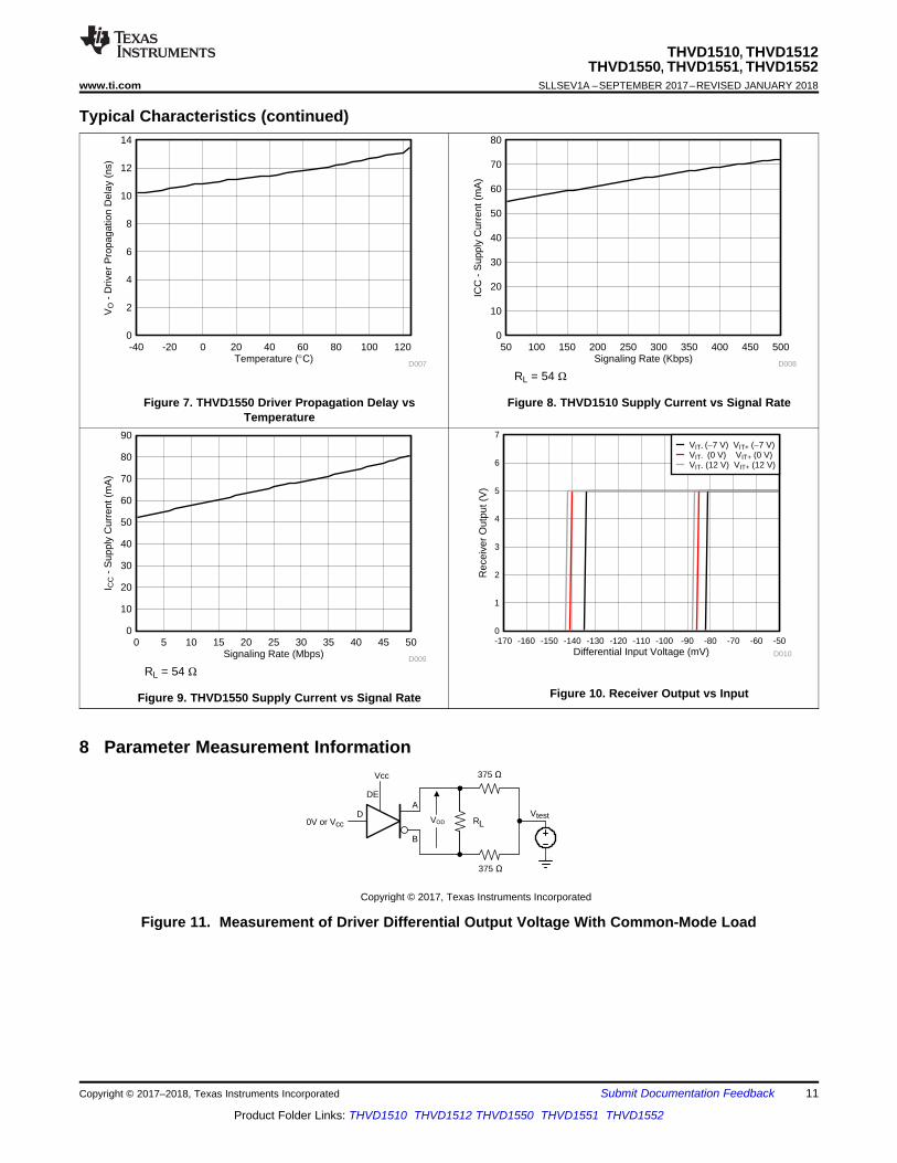
Typical Characteristics (continued)
Figure 7. THVD1550 Driver Propagation Delay vsTemperature
RL = 54 Ω
Figure 8. THVD1510 Supply Current vs Signal Rate
RL = 54 Ω
Figure 9. THVD1550 Supply Current vs Signal Rate Figure 10. Receiver Output vs Input
8 Parameter Measurement Information
Figure 11. Measurement of Driver Differential Output Voltage With Common-Mode Load

VOD
VI
tPLH tPHL
tr tf
90%
50 %
10 %
50%
3 V
VOH
VOL
0 V
Input
Generator
VO
VI50
RE
A
B
R
1.5V
0 V
CL=15 pF
Copyright © 2017, Texas Instruments Incorporated
VO
VI
tPZL tPLZ
50%
50 %
Vcc
Vcc
0 V
VOL
10%InputGenerator
A
BVOD
RL= 110
VI50
DE CL= 50 pF
S1
Vcc
§
Copyright © 2017, Texas Instruments Incorporated
VO
VI
tPZH
tPHZ
50%
50%
Vcc
~ 0V
0 V
VOH90%Input
Generator
A
B
VOD
RL = 110
VI 50
DECL = 50 pF
S1
~
Copyright © 2017, Texas Instruments Incorporated
VOD
VI
tPLH tPHL
tr tf
90%
50%
10%50%
Vcc
± 2 V
0 V
InputGenerator
A
B
Vcc
VODD RL=
54
VI 50
DE
CL= 50 pF
~~
~~2 V
Copyright © 2017, Texas Instruments Incorporated
A
B
VOC
VOC(PP) ûVOC(SS)
VA
VB0V or Vcc
A
B
DRL/2
CLVOC
VODRL/2
Copyright © 2017, Texas Instruments Incorporated
12
THVD1510, THVD1512THVD1550, THVD1551, THVD1552SLLSEV1A –SEPTEMBER 2017–REVISED JANUARY 2018 www.ti.com
Product Folder Links: THVD1510 THVD1512 THVD1550 THVD1551 THVD1552
Submit Documentation Feedback Copyright © 2017–2018, Texas Instruments Incorporated
Parameter Measurement Information (continued)
Figure 12. Measurement of Driver Differential and Common-Mode Output With RS-485 Load
Figure 13. Measurement of Driver Differential Output Rise and Fall Times and Propagation Delays
Figure 14. Measurement of Driver Enable and Disable Times With Active High Output and Pull-DownLoad
Figure 15. Measurement of Driver Enable and Disable Times With Active Low Output and Pull-up Load
Figure 16. Measurement of Receiver Output Rise and Fall Times and Propagation Delays

VO
VI
50%
Vcc
§0V
VOH
50%
VOL
VCC
tPZL(2)
VO
tPZH(2)
50%
InputGenerator
VO
VI50
A
B
R
CL=15 pF RE
V or 1.5V
Vcc
1 N
S11.5 V or 0V
0V
S1 to GND
A at 1.5VB at 0V
A at 0VB at 1.5VS1 to VCC
Copyright © 2017, Texas Instruments Incorporated
VO
VI
tPHZ
50 %
50 %
Vcc
0V
0V
VOH90%
50 %10%
VOL
VCC
tPLZtPZL(1)
VO
tPZH(1)
D at Vcc S1 to GND
InputGenerator
VO
VI50
A
B
R
CL=15 pF RE
0V or Vcc
DE
Vcc
D
Vcc
1 k
S1
§
D at 0V S1 to Vcc
Copyright © 2017, Texas Instruments Incorporated
13
THVD1510, THVD1512THVD1550, THVD1551, THVD1552
www.ti.com SLLSEV1A –SEPTEMBER 2017–REVISED JANUARY 2018
Product Folder Links: THVD1510 THVD1512 THVD1550 THVD1551 THVD1552
Submit Documentation FeedbackCopyright © 2017–2018, Texas Instruments Incorporated
Parameter Measurement Information (continued)
Figure 17. Measurement of Receiver Enable/Disable Times With Driver Enabled
Figure 18. Measurement of Receiver Enable Times With Driver Disabled

R
D
R
D
DE
RE
Y
Z
B
A
GND
VCC
Copyright © 2017, Texas Instruments Incorporated
R
D
R
DY
Z
B
A
VCC
GND
VCC
Copyright © 2017, Texas Instruments Incorporated
R
D
DE
RE
B
A
GND
VCC
Copyright © 2017, Texas Instruments Incorporated
14
THVD1510, THVD1512THVD1550, THVD1551, THVD1552SLLSEV1A –SEPTEMBER 2017–REVISED JANUARY 2018 www.ti.com
Product Folder Links: THVD1510 THVD1512 THVD1550 THVD1551 THVD1552
Submit Documentation Feedback Copyright © 2017–2018, Texas Instruments Incorporated
9 Detailed Description
9.1 OverviewTHVD1510 and THVD1550 are low-power, half-duplex RS-485 transceivers available in two speed gradessuitable for data transmission up to 500 kbps and 50 Mbps respectively.
THVD1551 is fully enabled with no external enabling pins. THVD1512 and THVD1552 have active-high driverenables and active-low receiver enables. A standby current of less than 1 µA can be achieved by disabling bothdriver and receiver.
9.2 Functional Block Diagrams
Figure 19. THVD1510 and THVD1550
Figure 20. THVD1551
Figure 21. THVD1512 and THVD1552

15
THVD1510, THVD1512THVD1550, THVD1551, THVD1552
www.ti.com SLLSEV1A –SEPTEMBER 2017–REVISED JANUARY 2018
Product Folder Links: THVD1510 THVD1512 THVD1550 THVD1551 THVD1552
Submit Documentation FeedbackCopyright © 2017–2018, Texas Instruments Incorporated
9.3 Feature DescriptionInternal ESD protection circuits of the THVD15xx protect the transceivers against electrostatic discharges (ESD)according to IEC 61000-4-2 of up to ±18 kV and against electrical fast transients (EFT) according to IEC 61000-4-4 of up to ±4 kV. With careful system design, one could achieve ±4 kV EFT Criterion A (no data loss whentransient noise is present).
The THVD15xx device family provides internal biasing of the receiver input thresholds in combination with largeinput-threshold hysteresis. The receiver output remains logic high under a bus-idle or bus-short conditionswithout the need for external failsafe biasing resistors. Device operation is specified over a wide ambienttemperature range from –40°C to 125°C.
9.4 Device Functional Modes
9.4.1 Device Functional Modes for THVD1510 and THVD1550When the driver enable pin, DE, is logic high, the differential outputs A and B follow the logic states at data inputD. A logic high at D causes A to turn high and B to turn low. In this case the differential output voltage defined asVOD = VA – VB is positive. When D is low, the output states reverse: B turns high, A becomes low, and VOD isnegative.
When DE is low, both outputs turn high-impedance. In this condition the logic state at D is irrelevant. The DE pinhas an internal pull-down resistor to ground, thus when left open the driver is disabled (high-impedance) bydefault. The D pin has an internal pull-up resistor to VCC, thus, when left open while the driver is enabled, outputA turns high and B turns low.
Table 1. Driver Function Table for THVD1510 and THVD1550INPUT ENABLE OUTPUTS
FUNCTIOND DE A BH H H L Actively drive bus highL H L H Actively drive bus lowX L Z Z Driver disabledX OPEN Z Z Driver disabled by default
OPEN H H L Actively drive bus high by default
When the receiver enable pin, RE, is logic low, the receiver is enabled. When the differential input voltagedefined as VID = VA – VB is higher than the positive input threshold, VTH+, the receiver output, R, turns high.When VID is lower than the negative input threshold, VTH-, the receiver output, R, turns low. If VID is between VTH+and VTH- the output is indeterminate.
When RE is logic high or left open, the receiver output is high-impedance and the magnitude and polarity of VIDare irrelevant. Internal biasing of the receiver inputs causes the output to go failsafe-high when the transceiver isdisconnected from the bus (open-circuit), the bus lines are shorted to one another (short-circuit), or the bus is notactively driven (idle bus).
Table 2. Receiver Function Table for THVD1510 and THVD1550DIFFERENTIAL INPUT ENABLE OUTPUT
FUNCTIONVID = VA – VB RE R
VTH+ < VID L H Receive valid bus highVTH- < VID < VTH+ L ? Indeterminate bus state
VID < VTH- L L Receive valid bus lowX H Z Receiver disabledX OPEN Z Receiver disabled by default
Open-circuit bus L H Fail-safe high outputShort-circuit bus L H Fail-safe high output
Idle (terminated) bus L H Fail-safe high output
16
THVD1510, THVD1512THVD1550, THVD1551, THVD1552SLLSEV1A –SEPTEMBER 2017–REVISED JANUARY 2018 www.ti.com
Product Folder Links: THVD1510 THVD1512 THVD1550 THVD1551 THVD1552
Submit Documentation Feedback Copyright © 2017–2018, Texas Instruments Incorporated
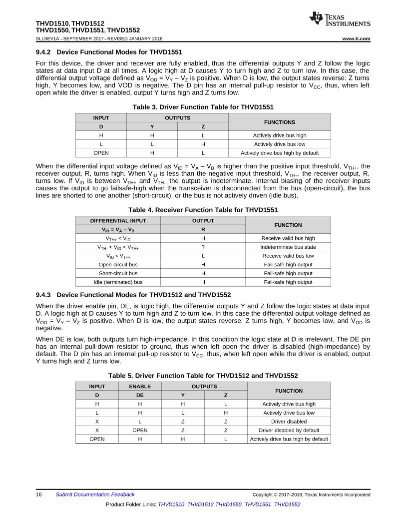
9.4.2 Device Functional Modes for THVD1551For this device, the driver and receiver are fully enabled, thus the differential outputs Y and Z follow the logicstates at data input D at all times. A logic high at D causes Y to turn high and Z to turn low. In this case, thedifferential output voltage defined as VOD = VY – VZ is positive. When D is low, the output states reverse: Z turnshigh, Y becomes low, and VOD is negative. The D pin has an internal pull-up resistor to VCC, thus, when leftopen while the driver is enabled, output Y turns high and Z turns low.
Table 3. Driver Function Table for THVD1551INPUT OUTPUTS
FUNCTIONSD Y ZH H L Actively drive bus highL L H Actively drive bus low
OPEN H L Actively drive bus high by default
When the differential input voltage defined as VID = VA – VB is higher than the positive input threshold, VTH+, thereceiver output, R, turns high. When VID is less than the negative input threshold, VTH–, the receiver output, R,turns low. If VID is between VTH+ and VTH– the output is indeterminate. Internal biasing of the receiver inputscauses the output to go failsafe-high when the transceiver is disconnected from the bus (open-circuit), the buslines are shorted to one another (short-circuit), or the bus is not actively driven (idle bus).
Table 4. Receiver Function Table for THVD1551DIFFERENTIAL INPUT OUTPUT
FUNCTIONVID = VA – VB R
VTH+ < VID H Receive valid bus highVTH- < VID < VTH+ ? Indeterminate bus state
VID < VTH- L Receive valid bus lowOpen-circuit bus H Fail-safe high outputShort-circuit bus H Fail-safe high output
Idle (terminated) bus H Fail-safe high output
9.4.3 Device Functional Modes for THVD1512 and THVD1552When the driver enable pin, DE, is logic high, the differential outputs Y and Z follow the logic states at data inputD. A logic high at D causes Y to turn high and Z to turn low. In this case the differential output voltage defined asVOD = VY – VZ is positive. When D is low, the output states reverse: Z turns high, Y becomes low, and VOD isnegative.
When DE is low, both outputs turn high-impedance. In this condition the logic state at D is irrelevant. The DE pinhas an internal pull-down resistor to ground, thus when left open the driver is disabled (high-impedance) bydefault. The D pin has an internal pull-up resistor to VCC, thus, when left open while the driver is enabled, outputY turns high and Z turns low.
Table 5. Driver Function Table for THVD1512 and THVD1552INPUT ENABLE OUTPUTS
FUNCTIOND DE Y ZH H H L Actively drive bus highL H L H Actively drive bus lowX L Z Z Driver disabledX OPEN Z Z Driver disabled by default
OPEN H H L Actively drive bus high by default

17
THVD1510, THVD1512THVD1550, THVD1551, THVD1552
www.ti.com SLLSEV1A –SEPTEMBER 2017–REVISED JANUARY 2018
Product Folder Links: THVD1510 THVD1512 THVD1550 THVD1551 THVD1552
Submit Documentation FeedbackCopyright © 2017–2018, Texas Instruments Incorporated
When the receiver enable pin, RE, is logic low, the receiver is enabled. When the differential input voltagedefined as VID = VA – VB is higher than the positive input threshold, VTH+, the receiver output, R, turns high.When VID is lower than the negative input threshold, VTH-, the receiver output, R, turns low. If VID is between VTH+and VTH- the output is indeterminate.
When RE is logic high or left open, the receiver output is high-impedance and the magnitude and polarity of VIDare irrelevant. Internal biasing of the receiver inputs causes the output to go failsafe-high when the transceiver isdisconnected from the bus (open-circuit), the bus lines are shorted to one another (short-circuit), or the bus is notactively driven (idle bus).
Table 6. Receiver Function Table for THVD1512 and THVD1552DIFFERENTIAL INPUT ENABLE OUTPUT
FUNCTIONVID = VA – VB RE R
VTH+ < VID L H Receive valid bus highVTH- < VID < VTH+ L ? Indeterminate bus state
VID < VTH- L L Receive valid bus lowX H Z Receiver disabledX OPEN Z Receiver disabled by default
Open-circuit bus L H Fail-safe high outputShort-circuit bus L H Fail-safe high output
Idle (terminated) bus L H Fail-safe high output

RT RT
R
DR
DE
RE
D
Y
Z R
D
R
RE
DE
D
A
B
RT RT
B
A
Z
Y
RD
R RE DE D
Z YBA
Master Slave
Slave
Copyright © 2017, Texas Instruments Incorporated
RT RT
R
A B
R RE DE D
DR
A B
R RE DE D
D
R
D
R
RE
DE
D
A
B
R
D
R
RE
DE
D
A
B
Copyright © 2017, Texas Instruments Incorporated
18
THVD1510, THVD1512THVD1550, THVD1551, THVD1552SLLSEV1A –SEPTEMBER 2017–REVISED JANUARY 2018 www.ti.com
Product Folder Links: THVD1510 THVD1512 THVD1550 THVD1551 THVD1552
Submit Documentation Feedback Copyright © 2017–2018, Texas Instruments Incorporated
10 Application and Implementation
NOTEInformation in the following applications sections is not part of the TI componentspecification, and TI does not warrant its accuracy or completeness. TI’s customers areresponsible for determining suitability of components for their purposes. Customers shouldvalidate and test their design implementation to confirm system functionality.
10.1 Application InformationThe THVD15xx family consists of half-duplex and full-duplex RS-485 transceivers commonly used forasynchronous data transmissions. For half-duplex devices, the driver and receiver enable pins allow for theconfiguration of different operating modes. Full-duplex implementation requires two signal pairs (four wires), andallows each node to transmit data on one pair while simultaneously receiving data on the other pair.
10.2 Typical ApplicationAn RS-485 bus consists of multiple transceivers connecting in parallel to a bus cable. To eliminate linereflections, each cable end is terminated with a termination resistor, RT, whose value matches the characteristicimpedance, Z0, of the cable. This method, known as parallel termination, generally allows for higher data ratesover longer cable length.
Figure 22. Typical RS-485 Network With Half-Duplex Transceivers
Figure 23. Typical RS-485 Network With Full-Duplex Transceivers

10000
1000
100
10
Cab
le L
en
gth
(ft
)
100 1k 10k 100k 1M 10M 100M
Data Rate (bps)
Conservative
Characteristics
5%, 10%, and 20% Jitter
19
THVD1510, THVD1512THVD1550, THVD1551, THVD1552
www.ti.com SLLSEV1A –SEPTEMBER 2017–REVISED JANUARY 2018
Product Folder Links: THVD1510 THVD1512 THVD1550 THVD1551 THVD1552
Submit Documentation FeedbackCopyright © 2017–2018, Texas Instruments Incorporated
Typical Application (continued)10.2.1 Design RequirementsRS-485 is a robust electrical standard suitable for long-distance networking that may be used in a wide range ofapplications with varying requirements, such as distance, data rate, and number of nodes.
10.2.1.1 Data Rate and Bus LengthThere is an inverse relationship between data rate and cable length, which means the higher the data rate, theshorter the cable length; and conversely, the lower the data rate, the longer the cable length. While most RS-485systems use data rates between 10 kbps and 100 kbps, some applications require data rates up to 250 kbps atdistances of 4000 feet and longer. Longer distances are possible by allowing for small signal jitter of up to 5 or10%.
Figure 24. Cable Length vs Data Rate Characteristic
Even higher data rates are achievable (that is, 50 Mbps for the THVD1550, THVD1551 and THVD1552) in caseswhere the interconnect is short enough (or has suitably low attenuation at signal frequencies) to not degrade thedata.
10.2.1.2 Stub LengthWhen connecting a node to the bus, the distance between the transceiver inputs and the cable trunk, known asthe stub, should be as short as possible. Stubs present a non-terminated piece of bus line which can introducereflections of varying phase as the length of the stub increases. As a general guideline, the electrical length, orround-trip delay, of a stub should be less than one-tenth of the rise time of the driver, thus giving a maximumphysical stub length as shown in Equation 1.
L(STUB) ≤ 0.1 × tr × v × c
where• tr is the 10/90 rise time of the driver• c is the speed of light (3 × 10⁸ m/s)• v is the signal velocity of the cable or trace as a factor of c (1)
10.2.1.3 Bus LoadingThe RS-485 standard specifies that a compliant driver must be able to drive 32 unit loads (UL), where 1 unit loadrepresents a load impedance of approximately 12 kΩ. Because the THVD15xx family consists of 1/8 ULtransceivers, connecting up to 256 receivers to the bus is possible.

20
THVD1510, THVD1512THVD1550, THVD1551, THVD1552SLLSEV1A –SEPTEMBER 2017–REVISED JANUARY 2018 www.ti.com
Product Folder Links: THVD1510 THVD1512 THVD1550 THVD1551 THVD1552
Submit Documentation Feedback Copyright © 2017–2018, Texas Instruments Incorporated
Typical Application (continued)10.2.1.4 Receiver FailsafeThe differential receivers of the THVD15xx family are failsafe to invalid bus states caused by the following:• Open bus conditions, such as a disconnected connector• Shorted bus conditions, such as cable damage shorting the twisted-pair together• Idle bus conditions that occur when no driver on the bus is actively driving
In any of these cases, the differential receiver will output a failsafe logic high state so that the output of thereceiver is not indeterminate.
Receiver failsafe is accomplished by offsetting the receiver thresholds such that the input indeterminate rangedoes not include zero volts differential. In order to comply with the RS-422 and RS-485 standards, the receiveroutput must output a high when the differential input VID is more positive than 200 mV, and must output a lowwhen VID is more negative than –200 mV. The receiver parameters which determine the failsafe performance areVTH+, VTH–, and VHYS (the separation between VTH+ and VTH–). As shown in the Electrical Characteristics table,differential signals more negative than –200 mV will always cause a low receiver output, and differential signalsmore positive than 200 mV will always cause a high receiver output.
When the differential input signal is close to zero, it is still above the VTH+ threshold, and the receiver output willbe high. Only when the differential input is more than VHYS below VTH+ will the receiver output transition to a lowstate. Therefore, the noise immunity of the receiver inputs during a bus fault conditions includes the receiverhysteresis value, Vhys, as well as the value of VTH+.

Pu
lse
Po
we
r (k
W)
22
20
18
16
14
12
10
8
6
4
2
0
Time (µs)
0 5 10 15 20 25 30 35 40
0.5-kV Surge
10-kV ESD
4-kV EFT
Pu
lse
Po
we
r (M
W) 2.2
2.0
1.8
1.6
1.4
1.2
1.0
0.8
0.6
0.4
0.2
0
Time (µs)
0 5 10 15 20 25 30 35 40
0.5-kV Surge
6-kV Surge
3.0
2.8
2.6
2.4
R(C) R(D)
C(S)
High-VoltagePulse
Generator
DeviceUnder
Test
Curr
ent
(A)
40
35
30
25
20
15
10
5
0
Time (ns)
0 50 100 150 200 250 300
10-kV IEC
10-kV HBM
330 Ω
(1.5 kΩ)
150 pF
(100 pF)
50 M
(1 M)
21
THVD1510, THVD1512THVD1550, THVD1551, THVD1552
www.ti.com SLLSEV1A –SEPTEMBER 2017–REVISED JANUARY 2018
Product Folder Links: THVD1510 THVD1512 THVD1550 THVD1551 THVD1552
Submit Documentation FeedbackCopyright © 2017–2018, Texas Instruments Incorporated
Typical Application (continued)10.2.1.5 Transient ProtectionThe bus pins of the THVD15xx transceiver family include on-chip ESD protection against ±30-kV HBM and ±18-kV IEC 61000-4-2 contact discharge. The International Electrotechnical Commission (IEC) ESD test is far moresevere than the HBM ESD test. The 50% higher charge capacitance, C(S), and 78% lower discharge resistance,R(D), of the IEC model produce significantly higher discharge currents than the HBM model. As stated in the IEC61000-4-2 standard, contact discharge is the preferred transient protection test method.
Figure 25. HBM and IEC ESD Models and Currents in Comparison (HBM Values in Parenthesis)
The on-chip implementation of IEC ESD protection significantly increases the robustness of equipment. Commondischarge events occur because of human contact with connectors and cables. Designers may choose toimplement protection against longer duration transients, typically referred to as surge transients.
EFTs are generally caused by relay-contact bounce or the interruption of inductive loads. Surge transients oftenresult from lightning strikes (direct strike or an indirect strike which induce voltages and currents), or theswitching of power systems, including load changes and short circuit switching. These transients are oftenencountered in industrial environments, such as factory automation and power-grid systems.
Figure 26 compares the pulse power of the EFT and surge transients with the power caused by an IEC ESDtransient. The left-hand diagram shows the relative pulse-power for a 0.5-kV surge transient and 4-kV EFTtransient, both of which dwarf the 10-kV ESD transient visible in the lower-left corner. 500-V surge transients arerepresentative of events that may occur in factory environments in industrial and process automation.
The right-hand diagram shows the pulse-power of a 6-kV surge transient, relative to the same 0.5-kV surgetransient. 6-kV surge transients are most likely to occur in power generation and power-grid systems.
Figure 26. Power Comparison of ESD, EFT, and Surge Transients
5V
VCC
GND
D
DE
R
RE
B
A
RxD
TxD
DIR
MCU/UART
10k
10k
TVS
R2
R1
100nF100nF
Copyright © 2017, Texas Instruments Incorporated
100
0.1
0.01
10
1
10-3
10-4
10-5
10-6
Pu
lse E
nerg
y (
J)
0.5 1 2 4 6 8 10
Peak Pulse Voltage (kV)
1000
ESD
EFT
Surge
15
EFT Pulse Train
22
THVD1510, THVD1512THVD1550, THVD1551, THVD1552SLLSEV1A –SEPTEMBER 2017–REVISED JANUARY 2018 www.ti.com
Product Folder Links: THVD1510 THVD1512 THVD1550 THVD1551 THVD1552
Submit Documentation Feedback Copyright © 2017–2018, Texas Instruments Incorporated
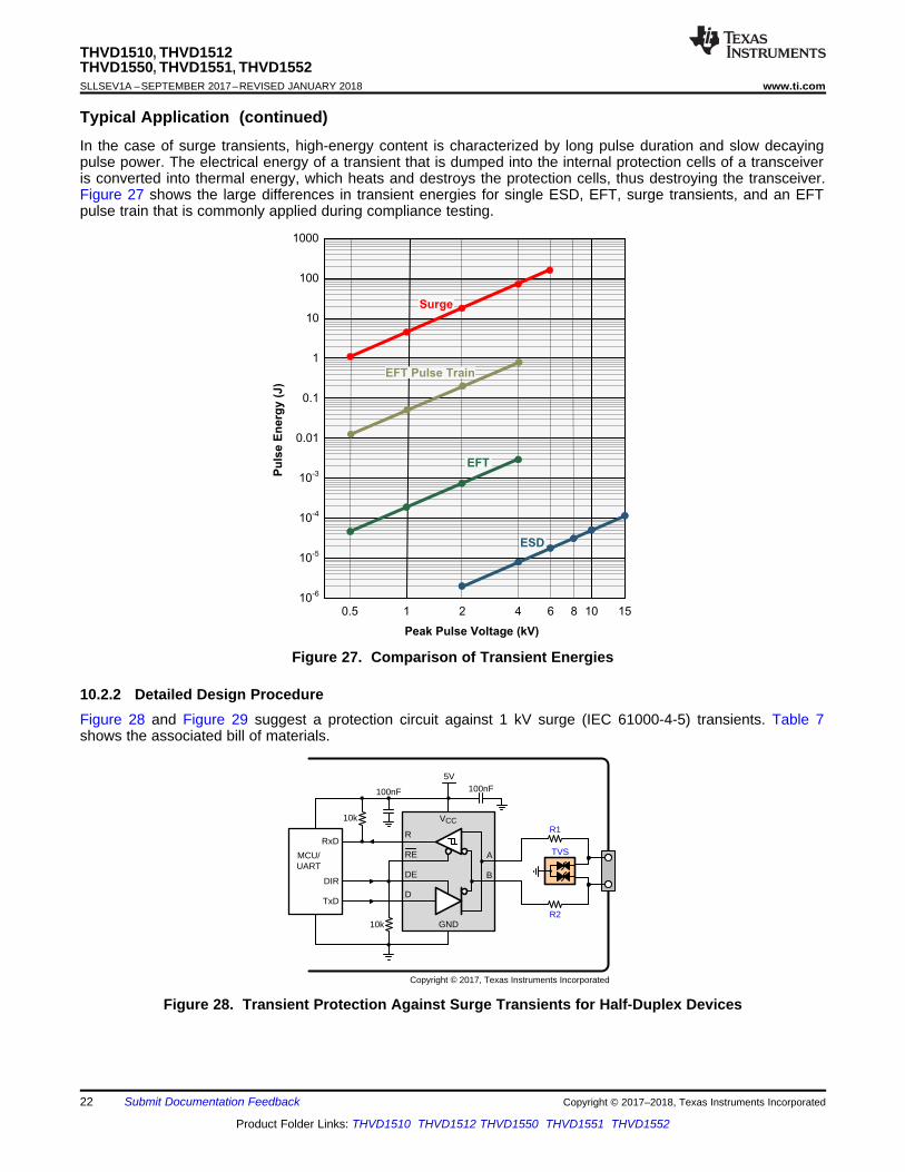
Typical Application (continued)In the case of surge transients, high-energy content is characterized by long pulse duration and slow decayingpulse power. The electrical energy of a transient that is dumped into the internal protection cells of a transceiveris converted into thermal energy, which heats and destroys the protection cells, thus destroying the transceiver.Figure 27 shows the large differences in transient energies for single ESD, EFT, surge transients, and an EFTpulse train that is commonly applied during compliance testing.
Figure 27. Comparison of Transient Energies
10.2.2 Detailed Design ProcedureFigure 28 and Figure 29 suggest a protection circuit against 1 kV surge (IEC 61000-4-5) transients. Table 7shows the associated bill of materials.
Figure 28. Transient Protection Against Surge Transients for Half-Duplex Devices

5V
VCC
GND
D
DE
R
RE
Y
Z
RxD
TxD
DIR
MCU/UART
10k
10k
TVS
R2
R1
100nF
TVS
R2
R1
DIR
B
A
Copyright © 2017, Texas Instruments Incorporated
23
THVD1510, THVD1512THVD1550, THVD1551, THVD1552
www.ti.com SLLSEV1A –SEPTEMBER 2017–REVISED JANUARY 2018
Product Folder Links: THVD1510 THVD1512 THVD1550 THVD1551 THVD1552
Submit Documentation FeedbackCopyright © 2017–2018, Texas Instruments Incorporated
Typical Application (continued)
Figure 29. Transient Protection Against Surge Transients for Full-Duplex Devices
Table 7. Bill of MaterialsDEVICE FUNCTION ORDER NUMBER MANUFACTURERXCVR 5-V, RS-485 transceiver THVD15xx TIR1
10-Ω, pulse-proof thick-film resistor CRCW0603010RJNEAHP VishayR2TVS Bidirectional 400-W transient suppressor CDSOT23-SM712 Bourns

24
THVD1510, THVD1512THVD1550, THVD1551, THVD1552SLLSEV1A –SEPTEMBER 2017–REVISED JANUARY 2018 www.ti.com
Product Folder Links: THVD1510 THVD1512 THVD1550 THVD1551 THVD1552
Submit Documentation Feedback Copyright © 2017–2018, Texas Instruments Incorporated
10.2.3 Application Curves
500 kbps
Figure 30. THVD1510 Waveforms with 60-Ω Termination
50 Mbps
Figure 31. THVD1550 Waveforms with 60-Ω Termination
11 Power Supply RecommendationsTo ensure reliable operation at all data rates and supply voltages, each supply should be decoupled with a 100nF ceramic capacitor located as close to the supply pins as possible. This helps to reduce supply voltage ripplepresent on the outputs of switched-mode power supplies and also helps to compensate for the resistance andinductance of the PCB power planes.

MCU
Via to ground
THVD15x0
JMPR
R
R
C
5
61
4R
5
Via to VCC
TVS5
6
25
THVD1510, THVD1512THVD1550, THVD1551, THVD1552
www.ti.com SLLSEV1A –SEPTEMBER 2017–REVISED JANUARY 2018
Product Folder Links: THVD1510 THVD1512 THVD1550 THVD1551 THVD1552
Submit Documentation FeedbackCopyright © 2017–2018, Texas Instruments Incorporated
12 Layout
12.1 Layout GuidelinesRobust and reliable bus node design often requires the use of external transient protection devices in order toprotect against surge transients that may occur in industrial environments. Since these transients have a widefrequency bandwidth (from approximately 3 MHz to 300 MHz), high-frequency layout techniques should beapplied during PCB design.1. Place the protection circuitry close to the bus connector to prevent noise transients from propagating across
the board.2. Use VCC and ground planes to provide low inductance. Note that high-frequency currents tend to follow the
path of least impedance and not the path of least resistance.3. Design the protection components into the direction of the signal path. Do not force the transient currents to
divert from the signal path to reach the protection device.4. Apply 100-nF to 220-nF decoupling capacitors as close as possible to the VCC pins of transceiver, UART
and/or controller ICs on the board.5. Use at least two vias for VCC and ground connections of decoupling capacitors and protection devices to
minimize effective via inductance.6. Use 1-kΩ to 10-kΩ pullup and pulldown resistors for enable lines to limit noise currents in these lines during
transient events.7. Insert pulse-proof resistors into the A and B bus lines if the TVS clamping voltage is higher than the specified
maximum voltage of the transceiver bus pins. These resistors limit the residual clamping current into thetransceiver and prevent it from latching up.
8. While pure TVS protection is sufficient for surge transients up to 1 kV, higher transients require metal-oxidevaristors (MOVs) which reduce the transients to a few hundred volts of clamping voltage, and transientblocking units (TBUs) that limit transient current to less than 1 mA.
12.2 Layout Example
Figure 32. Half-Duplex Layout Example

26
THVD1510, THVD1512THVD1550, THVD1551, THVD1552SLLSEV1A –SEPTEMBER 2017–REVISED JANUARY 2018 www.ti.com
Product Folder Links: THVD1510 THVD1512 THVD1550 THVD1551 THVD1552
Submit Documentation Feedback Copyright © 2017–2018, Texas Instruments Incorporated
13 Device and Documentation Support
13.1 Device Support
13.2 Third-Party Products DisclaimerTI'S PUBLICATION OF INFORMATION REGARDING THIRD-PARTY PRODUCTS OR SERVICES DOES NOTCONSTITUTE AN ENDORSEMENT REGARDING THE SUITABILITY OF SUCH PRODUCTS OR SERVICESOR A WARRANTY, REPRESENTATION OR ENDORSEMENT OF SUCH PRODUCTS OR SERVICES, EITHERALONE OR IN COMBINATION WITH ANY TI PRODUCT OR SERVICE.
13.3 Related LinksThe table below lists quick access links. Categories include technical documents, support and communityresources, tools and software, and quick access to order now.
Table 8. Related Links
PARTS PRODUCT FOLDER ORDER NOW TECHNICALDOCUMENTS
TOOLS &SOFTWARE
SUPPORT &COMMUNITY
THVD1510 Click here Click here Click here Click here Click hereTHVD1512 Click here Click here Click here Click here Click hereTHVD1550 Click here Click here Click here Click here Click hereTHVD1551 Click here Click here Click here Click here Click hereTHVD1552 Click here Click here Click here Click here Click here
13.4 Receiving Notification of Documentation UpdatesTo receive notification of documentation updates — go to the product folder for your device on ti.com. In theupper right-hand corner, click the Alert me button to register and receive a weekly digest of product informationthat has changed (if any). For change details, check the revision history of any revised document.
13.5 Community ResourcesThe following links connect to TI community resources. Linked contents are provided "AS IS" by the respectivecontributors. They do not constitute TI specifications and do not necessarily reflect TI's views; see TI's Terms ofUse.
TI E2E™ Online Community TI's Engineer-to-Engineer (E2E) Community. Created to foster collaborationamong engineers. At e2e.ti.com, you can ask questions, share knowledge, explore ideas and helpsolve problems with fellow engineers.
Design Support TI's Design Support Quickly find helpful E2E forums along with design support tools andcontact information for technical support.
13.6 TrademarksE2E is a trademark of Texas Instruments.
13.7 Electrostatic Discharge CautionThese devices have limited built-in ESD protection. The leads should be shorted together or the device placed in conductive foamduring storage or handling to prevent electrostatic damage to the MOS gates.
13.8 GlossarySLYZ022 — TI Glossary.
This glossary lists and explains terms, acronyms, and definitions.
27
THVD1510, THVD1512THVD1550, THVD1551, THVD1552
www.ti.com SLLSEV1A –SEPTEMBER 2017–REVISED JANUARY 2018
Product Folder Links: THVD1510 THVD1512 THVD1550 THVD1551 THVD1552
Submit Documentation FeedbackCopyright © 2017–2018, Texas Instruments Incorporated
14 Mechanical, Packaging, and Orderable InformationThe following pages include mechanical, packaging, and orderable information. This information is the mostcurrent data available for the designated devices. This data is subject to change without notice and revision ofthis document. For browser-based versions of this data sheet, refer to the left-hand navigation.

www.ti.com
PACKAGE OUTLINE
C
TYP-.244.228-6.195.80[ ]
.069 MAX[1.75]
6X .050[1.27]
8X .012-.020[0.31-0.51]
2X
.150[3.81]
TYP-.010.005-0.250.13[ ]
0 - 8-.010.004-0.250.11[ ]
.010[0.25]
-.050.016-1.270.41[ ]
.041[1.04]
A
NOTE 3
-.197.189-5.004.81[ ]
B
NOTE 4
-.157.150-3.983.81[ ]
SOIC
SOIC - 1.75 mm max heightD0008B
4221445/B 04/2014
NOTES:
1. Linear dimensions are in inches [millimeters]. Dimensions in parenthesis are for reference only. Controlling dimensions are in inches.Dimensioning and tolerancing per ASME Y14.5M.
2. This drawing is subject to change without notice.3. This dimension does not include mold flash, protrusions, or gate burrs. Mold flash, protrusions, or gate burrs shall not
exceed .006 [0.15], per side.4. This dimension does not include interlead flash.5. Reference JEDEC registration MS-012, variation AA.
18
.010 [0.25] C A B
5
4
PIN 1 ID AREA
SEATING PLANE
.004 [0.1] C
SEE DETAIL A
TYPICALDETAIL A
SCALE 2.800
28
THVD1510, THVD1512THVD1550, THVD1551, THVD1552SLLSEV1A –SEPTEMBER 2017–REVISED JANUARY 2018 www.ti.com
Product Folder Links: THVD1510 THVD1512 THVD1550 THVD1551 THVD1552
Submit Documentation Feedback Copyright © 2017–2018, Texas Instruments Incorporated

www.ti.com
EXAMPLE BOARD LAYOUT
.0028 MAX[0.07]ALL AROUND
.0028 MIN[0.07]ALL AROUND
(.213)[5.4]
6X (.050 )[1.27]
(.217)[5.5]
8X (.061 )[1.55]
8X (.024)[0.6]
8X (.055)[1.4]
8X (.024)[0.6]
6X (.050 )[1.27]
SOIC
SOIC - 1.75 mm max heightD0008B
4221445/B 04/2014
NOTES: (continued)
6. Publication IPC-7351 may have alternate designs.7. Solder mask tolerances between and around signal pads can vary based on board fabrication site.
METALSOLDER MASKOPENING
NON SOLDER MASKDEFINED
OPENING
SOLDER MASK DETAILS
SOLDER MASK METAL
SOLDER MASKDEFINED
SCALE:6XLAND PATTERN EXAMPLE
SYMM
1
45
8
SEEDETAILS
IPC-7351 NOMINAL.150 [3.85] CLEARANCE / CREEPAGE
SYMM
HV / ISOLATION OPTION.162 [4.1] CLEARANCE / CREEPAGE
SYMM
1
45
8
SEEDETAILS
SYMM
29
THVD1510, THVD1512THVD1550, THVD1551, THVD1552
www.ti.com SLLSEV1A –SEPTEMBER 2017–REVISED JANUARY 2018
Product Folder Links: THVD1510 THVD1512 THVD1550 THVD1551 THVD1552
Submit Documentation FeedbackCopyright © 2017–2018, Texas Instruments Incorporated

www.ti.com
EXAMPLE STENCIL DESIGN
8X (.061 )[1.55]
8X (.024)[0.6]
6X (.050 )[1.27]
(.213)[5.4]
8X (.055)[1.4]
8X (.024)[0.6]
6X (.050 )[1.27]
(.217)[5.5]
SOIC
SOIC - 1.75 mm max heightD0008B
4221445/B 04/2014
NOTES: (continued)
8. Laser cutting apertures with trapezoidal walls and rounded corners may offer better paste release. IPC-7525 may have alternatedesign recommendations.
9. Board assembly site may have different recommendations for stencil design.
HV / ISOLATION OPTION.162 [4.1] CLEARANCE / CREEPAGE
BASED ON .005 INCH [0.127 MM] THICK STENCILSOLDER PASTE EXAMPLE
SCALE:6X
SYMM
SYMM
1
45
8
IPC-7351 NOMINAL.150 [3.85] CLEARANCE / CREEPAGE
SYMM
SYMM
1
45
8
30
THVD1510, THVD1512THVD1550, THVD1551, THVD1552SLLSEV1A –SEPTEMBER 2017–REVISED JANUARY 2018 www.ti.com
Product Folder Links: THVD1510 THVD1512 THVD1550 THVD1551 THVD1552
Submit Documentation Feedback Copyright © 2017–2018, Texas Instruments Incorporated

31
THVD1510, THVD1512THVD1550, THVD1551, THVD1552
www.ti.com SLLSEV1A –SEPTEMBER 2017–REVISED JANUARY 2018
Product Folder Links: THVD1510 THVD1512 THVD1550 THVD1551 THVD1552
Submit Documentation FeedbackCopyright © 2017–2018, Texas Instruments Incorporated

32
THVD1510, THVD1512THVD1550, THVD1551, THVD1552SLLSEV1A –SEPTEMBER 2017–REVISED JANUARY 2018 www.ti.com
Product Folder Links: THVD1510 THVD1512 THVD1550 THVD1551 THVD1552
Submit Documentation Feedback Copyright © 2017–2018, Texas Instruments Incorporated

33
THVD1510, THVD1512THVD1550, THVD1551, THVD1552
www.ti.com SLLSEV1A –SEPTEMBER 2017–REVISED JANUARY 2018
Product Folder Links: THVD1510 THVD1512 THVD1550 THVD1551 THVD1552
Submit Documentation FeedbackCopyright © 2017–2018, Texas Instruments Incorporated

www.ti.com
PACKAGE OUTLINE
C
TYP5.054.75
1.1 MAX
8X 0.5
10X0.270.17
2X
2
0.150.05
TYP0.230.13
0 - 8
0.25
GAGE PLANE
0.70.4
A
NOTE 3
3.12.9
B
NOTE 4
3.12.9
4221984/A 05/2015
VSSOP - 1.1 mm max heightDGS0010ASMALL OUTLINE PACKAGE
NOTES:
1. All linear dimensions are in millimeters. Any dimensions in parenthesis are for reference only. Dimensioning and tolerancingper ASME Y14.5M.
2. This drawing is subject to change without notice.3. This dimension does not include mold flash, protrusions, or gate burrs. Mold flash, protrusions, or gate burrs shall not
exceed 0.15 mm per side.4. This dimension does not include interlead flash. Interlead flash shall not exceed 0.25 mm per side.5. Reference JEDEC registration MO-187, variation BA.
110
0.1 C A B
6
5
PIN 1 IDAREA
SEATING PLANE
0.1 C
SEE DETAIL A
TYPICALDETAIL A
SCALE 3.200
34
THVD1510, THVD1512THVD1550, THVD1551, THVD1552SLLSEV1A –SEPTEMBER 2017–REVISED JANUARY 2018 www.ti.com
Product Folder Links: THVD1510 THVD1512 THVD1550 THVD1551 THVD1552
Submit Documentation Feedback Copyright © 2017–2018, Texas Instruments Incorporated

www.ti.com
EXAMPLE BOARD LAYOUT
(4.4)
0.05 MAXALL AROUND
0.05 MINALL AROUND
10X (1.45)
10X (0.3)
8X (0.5)
(R )TYP
0.05
4221984/A 05/2015
SYMM
VSSOP - 1.1 mm max heightDGS0010ASMALL OUTLINE PACKAGE
SYMM
LAND PATTERN EXAMPLESCALE:10X
1
5 6
10
NOTES: (continued)
6. Publication IPC-7351 may have alternate designs.7. Solder mask tolerances between and around signal pads can vary based on board fabrication site.
METALSOLDER MASKOPENING
NON SOLDER MASKDEFINED
NOT TO SCALESOLDER MASK DETAILS
SOLDER MASKOPENING
METAL UNDERSOLDER MASK
SOLDER MASKDEFINED
35
THVD1510, THVD1512THVD1550, THVD1551, THVD1552
www.ti.com SLLSEV1A –SEPTEMBER 2017–REVISED JANUARY 2018
Product Folder Links: THVD1510 THVD1512 THVD1550 THVD1551 THVD1552
Submit Documentation FeedbackCopyright © 2017–2018, Texas Instruments Incorporated

www.ti.com
EXAMPLE STENCIL DESIGN
(4.4)
8X (0.5)
10X (0.3)
10X (1.45)(R ) TYP0.05
4221984/A 05/2015
VSSOP - 1.1 mm max heightDGS0010ASMALL OUTLINE PACKAGE
NOTES: (continued)
8. Laser cutting apertures with trapezoidal walls and rounded corners may offer better paste release. IPC-7525 may have alternatedesign recommendations.
9. Board assembly site may have different recommendations for stencil design.
SYMM
SYMM
1
5 6
10
BASED ON 0.125 mm THICK STENCILSOLDER PASTE EXAMPLE
SCALE:10X
36
THVD1510, THVD1512THVD1550, THVD1551, THVD1552SLLSEV1A –SEPTEMBER 2017–REVISED JANUARY 2018 www.ti.com
Product Folder Links: THVD1510 THVD1512 THVD1550 THVD1551 THVD1552
Submit Documentation Feedback Copyright © 2017–2018, Texas Instruments Incorporated

PACKAGE OPTION ADDENDUM
www.ti.com 20-Apr-2018
Addendum-Page 1
PACKAGING INFORMATION
Orderable Device Status(1)
Package Type PackageDrawing
Pins PackageQty
Eco Plan(2)
Lead/Ball Finish(6)
MSL Peak Temp(3)
Op Temp (°C) Device Marking(4/5)
Samples
THVD1510D ACTIVE SOIC D 8 75 Green (RoHS& no Sb/Br)
CU NIPDAU Level-1-260C-UNLIM -40 to 125 VD1510
THVD1510DGK ACTIVE VSSOP DGK 8 80 Green (RoHS& no Sb/Br)
CU NIPDAUAG Level-1-260C-UNLIM -40 to 125 1510
THVD1510DGKR ACTIVE VSSOP DGK 8 2500 Green (RoHS& no Sb/Br)
CU NIPDAUAG Level-1-260C-UNLIM -40 to 125 1510
THVD1510DR ACTIVE SOIC D 8 2500 Green (RoHS& no Sb/Br)
CU NIPDAU Level-1-260C-UNLIM -40 to 125 VD1510
THVD1512D PREVIEW SOIC D 14 75 TBD Call TI Call TI -40 to 125
THVD1512DGS ACTIVE VSSOP DGS 10 80 Green (RoHS& no Sb/Br)
CU NIPDAUAG Level-1-260C-UNLIM -40 to 125 1512
THVD1512DGSR ACTIVE VSSOP DGS 10 2500 Green (RoHS& no Sb/Br)
CU NIPDAUAG Level-1-260C-UNLIM -40 to 125 1512
THVD1512DR PREVIEW SOIC D 14 2500 TBD Call TI Call TI -40 to 125
THVD1550D ACTIVE SOIC D 8 75 Green (RoHS& no Sb/Br)
CU NIPDAU Level-1-260C-UNLIM -40 to 125 VD1550
THVD1550DGK ACTIVE VSSOP DGK 8 80 Green (RoHS& no Sb/Br)
CU NIPDAUAG Level-1-260C-UNLIM -40 to 125 1550
THVD1550DGKR ACTIVE VSSOP DGK 8 2500 Green (RoHS& no Sb/Br)
CU NIPDAUAG Level-1-260C-UNLIM -40 to 125 1550
THVD1550DR ACTIVE SOIC D 8 2500 Green (RoHS& no Sb/Br)
CU NIPDAU Level-1-260C-UNLIM -40 to 125 VD1550
THVD1551DGK ACTIVE VSSOP DGK 8 80 Green (RoHS& no Sb/Br)
CU NIPDAUAG Level-1-260C-UNLIM -40 to 125 1551
THVD1551DGKR ACTIVE VSSOP DGK 8 2500 Green (RoHS& no Sb/Br)
CU NIPDAUAG Level-1-260C-UNLIM -40 to 125 1551
THVD1552D ACTIVE SOIC D 14 50 Green (RoHS& no Sb/Br)
CU NIPDAU Level-1-260C-UNLIM -40 to 125 1552
THVD1552DGS ACTIVE VSSOP DGS 10 80 Green (RoHS& no Sb/Br)
CU NIPDAUAG Level-1-260C-UNLIM -40 to 125 1552
THVD1552DGSR ACTIVE VSSOP DGS 10 2500 Green (RoHS& no Sb/Br)
CU NIPDAUAG Level-1-260C-UNLIM -40 to 125 1552
THVD1552DR ACTIVE SOIC D 14 2500 Green (RoHS& no Sb/Br)
CU NIPDAU Level-1-260C-UNLIM -40 to 125 1552

PACKAGE OPTION ADDENDUM
www.ti.com 20-Apr-2018
Addendum-Page 2
(1) The marketing status values are defined as follows:ACTIVE: Product device recommended for new designs.LIFEBUY: TI has announced that the device will be discontinued, and a lifetime-buy period is in effect.NRND: Not recommended for new designs. Device is in production to support existing customers, but TI does not recommend using this part in a new design.PREVIEW: Device has been announced but is not in production. Samples may or may not be available.OBSOLETE: TI has discontinued the production of the device.
(2) RoHS: TI defines "RoHS" to mean semiconductor products that are compliant with the current EU RoHS requirements for all 10 RoHS substances, including the requirement that RoHS substancedo not exceed 0.1% by weight in homogeneous materials. Where designed to be soldered at high temperatures, "RoHS" products are suitable for use in specified lead-free processes. TI mayreference these types of products as "Pb-Free".RoHS Exempt: TI defines "RoHS Exempt" to mean products that contain lead but are compliant with EU RoHS pursuant to a specific EU RoHS exemption.Green: TI defines "Green" to mean the content of Chlorine (Cl) and Bromine (Br) based flame retardants meet JS709B low halogen requirements of <=1000ppm threshold. Antimony trioxide basedflame retardants must also meet the <=1000ppm threshold requirement.
(3) MSL, Peak Temp. - The Moisture Sensitivity Level rating according to the JEDEC industry standard classifications, and peak solder temperature.
(4) There may be additional marking, which relates to the logo, the lot trace code information, or the environmental category on the device.
(5) Multiple Device Markings will be inside parentheses. Only one Device Marking contained in parentheses and separated by a "~" will appear on a device. If a line is indented then it is a continuationof the previous line and the two combined represent the entire Device Marking for that device.
(6) Lead/Ball Finish - Orderable Devices may have multiple material finish options. Finish options are separated by a vertical ruled line. Lead/Ball Finish values may wrap to two lines if the finishvalue exceeds the maximum column width.
Important Information and Disclaimer:The information provided on this page represents TI's knowledge and belief as of the date that it is provided. TI bases its knowledge and belief on informationprovided by third parties, and makes no representation or warranty as to the accuracy of such information. Efforts are underway to better integrate information from third parties. TI has taken andcontinues to take reasonable steps to provide representative and accurate information but may not have conducted destructive testing or chemical analysis on incoming materials and chemicals.TI and TI suppliers consider certain information to be proprietary, and thus CAS numbers and other limited information may not be available for release.
In no event shall TI's liability arising out of such information exceed the total purchase price of the TI part(s) at issue in this document sold by TI to Customer on an annual basis.

TAPE AND REEL INFORMATION
*All dimensions are nominal
Device PackageType
PackageDrawing
Pins SPQ ReelDiameter
(mm)
ReelWidth
W1 (mm)
A0(mm)
B0(mm)
K0(mm)
P1(mm)
W(mm)
Pin1Quadrant
THVD1510DGKR VSSOP DGK 8 2500 330.0 12.4 5.3 3.4 1.4 8.0 12.0 Q1
THVD1510DR SOIC D 8 2500 330.0 12.4 6.4 5.2 2.1 8.0 12.0 Q1
THVD1512DGSR VSSOP DGS 10 2500 330.0 12.4 5.3 3.4 1.4 8.0 12.0 Q1
THVD1550DGKR VSSOP DGK 8 2500 330.0 12.4 5.3 3.4 1.4 8.0 12.0 Q1
THVD1550DR SOIC D 8 2500 330.0 12.4 6.4 5.2 2.1 8.0 12.0 Q1
THVD1551DGKR VSSOP DGK 8 2500 330.0 12.4 5.3 3.4 1.4 8.0 12.0 Q1
THVD1552DGSR VSSOP DGS 10 2500 330.0 12.4 5.3 3.4 1.4 8.0 12.0 Q1
THVD1552DR SOIC D 14 2500 330.0 16.4 6.5 9.0 2.1 8.0 16.0 Q1
PACKAGE MATERIALS INFORMATION
www.ti.com 30-Apr-2018
Pack Materials-Page 1

*All dimensions are nominal
Device Package Type Package Drawing Pins SPQ Length (mm) Width (mm) Height (mm)
THVD1510DGKR VSSOP DGK 8 2500 364.0 364.0 27.0
THVD1510DR SOIC D 8 2500 340.5 338.1 20.6
THVD1512DGSR VSSOP DGS 10 2500 364.0 364.0 27.0
THVD1550DGKR VSSOP DGK 8 2500 364.0 364.0 27.0
THVD1550DR SOIC D 8 2500 340.5 338.1 20.6
THVD1551DGKR VSSOP DGK 8 2500 364.0 364.0 27.0
THVD1552DGSR VSSOP DGS 10 2500 364.0 364.0 27.0
THVD1552DR SOIC D 14 2500 333.2 345.9 28.6
PACKAGE MATERIALS INFORMATION
www.ti.com 30-Apr-2018
Pack Materials-Page 2

IMPORTANT NOTICE
Texas Instruments Incorporated (TI) reserves the right to make corrections, enhancements, improvements and other changes to itssemiconductor products and services per JESD46, latest issue, and to discontinue any product or service per JESD48, latest issue. Buyersshould obtain the latest relevant information before placing orders and should verify that such information is current and complete.TI’s published terms of sale for semiconductor products (http://www.ti.com/sc/docs/stdterms.htm) apply to the sale of packaged integratedcircuit products that TI has qualified and released to market. Additional terms may apply to the use or sale of other types of TI products andservices.Reproduction of significant portions of TI information in TI data sheets is permissible only if reproduction is without alteration and isaccompanied by all associated warranties, conditions, limitations, and notices. TI is not responsible or liable for such reproduceddocumentation. Information of third parties may be subject to additional restrictions. Resale of TI products or services with statementsdifferent from or beyond the parameters stated by TI for that product or service voids all express and any implied warranties for theassociated TI product or service and is an unfair and deceptive business practice. TI is not responsible or liable for any such statements.Buyers and others who are developing systems that incorporate TI products (collectively, “Designers”) understand and agree that Designersremain responsible for using their independent analysis, evaluation and judgment in designing their applications and that Designers havefull and exclusive responsibility to assure the safety of Designers' applications and compliance of their applications (and of all TI productsused in or for Designers’ applications) with all applicable regulations, laws and other applicable requirements. Designer represents that, withrespect to their applications, Designer has all the necessary expertise to create and implement safeguards that (1) anticipate dangerousconsequences of failures, (2) monitor failures and their consequences, and (3) lessen the likelihood of failures that might cause harm andtake appropriate actions. Designer agrees that prior to using or distributing any applications that include TI products, Designer willthoroughly test such applications and the functionality of such TI products as used in such applications.TI’s provision of technical, application or other design advice, quality characterization, reliability data or other services or information,including, but not limited to, reference designs and materials relating to evaluation modules, (collectively, “TI Resources”) are intended toassist designers who are developing applications that incorporate TI products; by downloading, accessing or using TI Resources in anyway, Designer (individually or, if Designer is acting on behalf of a company, Designer’s company) agrees to use any particular TI Resourcesolely for this purpose and subject to the terms of this Notice.TI’s provision of TI Resources does not expand or otherwise alter TI’s applicable published warranties or warranty disclaimers for TIproducts, and no additional obligations or liabilities arise from TI providing such TI Resources. TI reserves the right to make corrections,enhancements, improvements and other changes to its TI Resources. TI has not conducted any testing other than that specificallydescribed in the published documentation for a particular TI Resource.Designer is authorized to use, copy and modify any individual TI Resource only in connection with the development of applications thatinclude the TI product(s) identified in such TI Resource. NO OTHER LICENSE, EXPRESS OR IMPLIED, BY ESTOPPEL OR OTHERWISETO ANY OTHER TI INTELLECTUAL PROPERTY RIGHT, AND NO LICENSE TO ANY TECHNOLOGY OR INTELLECTUAL PROPERTYRIGHT OF TI OR ANY THIRD PARTY IS GRANTED HEREIN, including but not limited to any patent right, copyright, mask work right, orother intellectual property right relating to any combination, machine, or process in which TI products or services are used. Informationregarding or referencing third-party products or services does not constitute a license to use such products or services, or a warranty orendorsement thereof. Use of TI Resources may require a license from a third party under the patents or other intellectual property of thethird party, or a license from TI under the patents or other intellectual property of TI.TI RESOURCES ARE PROVIDED “AS IS” AND WITH ALL FAULTS. TI DISCLAIMS ALL OTHER WARRANTIES ORREPRESENTATIONS, EXPRESS OR IMPLIED, REGARDING RESOURCES OR USE THEREOF, INCLUDING BUT NOT LIMITED TOACCURACY OR COMPLETENESS, TITLE, ANY EPIDEMIC FAILURE WARRANTY AND ANY IMPLIED WARRANTIES OFMERCHANTABILITY, FITNESS FOR A PARTICULAR PURPOSE, AND NON-INFRINGEMENT OF ANY THIRD PARTY INTELLECTUALPROPERTY RIGHTS. TI SHALL NOT BE LIABLE FOR AND SHALL NOT DEFEND OR INDEMNIFY DESIGNER AGAINST ANY CLAIM,INCLUDING BUT NOT LIMITED TO ANY INFRINGEMENT CLAIM THAT RELATES TO OR IS BASED ON ANY COMBINATION OFPRODUCTS EVEN IF DESCRIBED IN TI RESOURCES OR OTHERWISE. IN NO EVENT SHALL TI BE LIABLE FOR ANY ACTUAL,DIRECT, SPECIAL, COLLATERAL, INDIRECT, PUNITIVE, INCIDENTAL, CONSEQUENTIAL OR EXEMPLARY DAMAGES INCONNECTION WITH OR ARISING OUT OF TI RESOURCES OR USE THEREOF, AND REGARDLESS OF WHETHER TI HAS BEENADVISED OF THE POSSIBILITY OF SUCH DAMAGES.Unless TI has explicitly designated an individual product as meeting the requirements of a particular industry standard (e.g., ISO/TS 16949and ISO 26262), TI is not responsible for any failure to meet such industry standard requirements.Where TI specifically promotes products as facilitating functional safety or as compliant with industry functional safety standards, suchproducts are intended to help enable customers to design and create their own applications that meet applicable functional safety standardsand requirements. Using products in an application does not by itself establish any safety features in the application. Designers mustensure compliance with safety-related requirements and standards applicable to their applications. Designer may not use any TI products inlife-critical medical equipment unless authorized officers of the parties have executed a special contract specifically governing such use.Life-critical medical equipment is medical equipment where failure of such equipment would cause serious bodily injury or death (e.g., lifesupport, pacemakers, defibrillators, heart pumps, neurostimulators, and implantables). Such equipment includes, without limitation, allmedical devices identified by the U.S. Food and Drug Administration as Class III devices and equivalent classifications outside the U.S.TI may expressly designate certain products as completing a particular qualification (e.g., Q100, Military Grade, or Enhanced Product).Designers agree that it has the necessary expertise to select the product with the appropriate qualification designation for their applicationsand that proper product selection is at Designers’ own risk. Designers are solely responsible for compliance with all legal and regulatoryrequirements in connection with such selection.Designer will fully indemnify TI and its representatives against any damages, costs, losses, and/or liabilities arising out of Designer’s non-compliance with the terms and provisions of this Notice.
Mailing Address: Texas Instruments, Post Office Box 655303, Dallas, Texas 75265Copyright © 2018, Texas Instruments Incorporated