

SLLS779B JANUARY 2008 REVISED APRIL 2008 1 …static.advonics.com/content/pdfs/216/6914404.pdf ·...
26
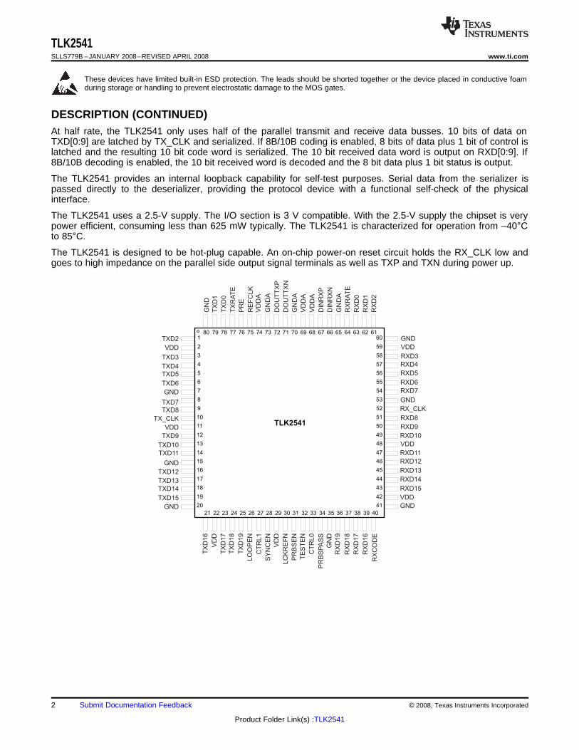
TLK2541 www.ti.com SLLS779B – JANUARY 2008 – REVISED APRIL 2008 1 TO 2.6 GBPS TRANSCEIVER Check for Samples: TLK2541 1FEATURES • Receiver Differential Input Thresholds 200 mV Minimum 2• 1 to 2.6 Gigabits Per Second (Gbps) Serializer/Deserializer • 3 V Tolerance on Parallel Data Input Signals • Independent Transmit/Receive Channels for • Selectable 10 or 20 bit Parallel TTL Compatible Asynchronous Data Rate Operation Data Interface • Fast Relock at 1.25 Gbps and 2.5 Gbps for • Industrial Temperature Range –40°C to 85°C EPON OLT Applications • Integrated 50-Ω Termination Resistors on RX • Hot-Plug Protection • Transmit FIFO Decouples Transmit Clock • High-Performance 80-Pin TQFP Package (PFP) From Reference Clock • 2.5-V Power Supply for Low Power Operation APPLICATIONS • Programmable Preemphasis Levels on Serial • Next Generation EPON OLT Systems Output • Ideal for use with EPON OLT MAC Solutions • Interfaces to Backplane, Copper Cables, or such as TK3723 from Teknovus Optical Converters • Gigabit Ethernet and Fibre Channel Links • On-Chip 8-bit/10-bit Encoding/Decoding • On-Chip PLL Provides Clock Synthesis From Low-Speed Reference DESCRIPTION The TLK2541 is a member of the WizardLink transceiver family of multigigabit transceivers, intended for use in high-speed bidirectional point-to-point data transmission systems. The TLK2541 supports an effective serial interface speed of 1 Gbps to 1.3 Gbps or 2 to 2.6 Gbps, providing over 2 Gbps of data bandwidth. The primary application of this chip is to provide high-speed I/O data channels for point-to-point baseband data transmission over controlled impedance media of approximately 50Ω. The transmission media can be printed-circuit board, copper cables, or fiber-optic cable. The maximum rate and distance of data transfer is dependent upon the attenuation characteristics of the media and the noise coupling to the environment. The TLK2541 allows for independent transmit and receive data rate operation for applications that need asymmetrical data rates such as Passive Optical Networking. This device can also be used to replace parallel data transmission architectures by providing a reduction in the number of traces, connector terminals, and transmit/receive terminals. Parallel data loaded into the transmitter is delivered to the receiver over a serial channel, which can be a coaxial copper cable, a controlled impedance backplane, or an optical link. It is then reconstructed into its original parallel format. It offers significant power and cost savings over parallel solutions, as well as scalability for higher data rates. At full rate, the TLK2541 performs data conversion parallel-to-serial and serial-to-parallel. The clock extraction functions as a physical layer interface device. The serial transceiver interface operates at a maximum speed of 2.6 Gbps. The transmitter latches 20 parallel data at a rate based on the supplied transmit clock (TX_CLK).. The 20-bit word is then transmitted differentially at 20 times the reference clock (REFCLK) rate. The receiver section performs the serial-to-parallel conversion on the input data, synchronizing the resulting 20-bit wide parallel data to the recovered clock (RX_CLK). It then outputs the 20 bit recovered word on the receive data terminals RXD[0:19]. If the internal 8B/10B coding and decoding logic is enabled, 16 bits of data and two bits of control are latched on TX_CLK and the data is encoded into a 20 bit data word to be serialized. Likewise the 20 bit received data word is decoded into a 16 bit data word plus two bits of decode status. 1 Please be aware that an important notice concerning availability, standard warranty, and use in critical applications of Texas Instruments semiconductor products and disclaimers thereto appears at the end of this data sheet. 2PowerPAD is a trademark of Texas Instruments. PRODUCTION DATA information is current as of publication date. © 2008, Texas Instruments Incorporated Products conform to specifications per the terms of the Texas Instruments standard warranty. Production processing does not necessarily include testing of all parameters.
Transcript of SLLS779B JANUARY 2008 REVISED APRIL 2008 1 …static.advonics.com/content/pdfs/216/6914404.pdf ·...

TLK2541www.ti.com SLLS779B –JANUARY 2008–REVISED APRIL 2008
1 TO 2.6 GBPS TRANSCEIVERCheck for Samples: TLK2541
1FEATURES • Receiver Differential Input Thresholds 200 mVMinimum
2• 1 to 2.6 Gigabits Per Second (Gbps)Serializer/Deserializer • 3 V Tolerance on Parallel Data Input Signals
• Independent Transmit/Receive Channels for • Selectable 10 or 20 bit Parallel TTL CompatibleAsynchronous Data Rate Operation Data Interface
• Fast Relock at 1.25 Gbps and 2.5 Gbps for • Industrial Temperature Range –40°C to 85°CEPON OLT Applications • Integrated 50-Ω Termination Resistors on RX
• Hot-Plug Protection • Transmit FIFO Decouples Transmit Clock• High-Performance 80-Pin TQFP Package (PFP) From Reference Clock• 2.5-V Power Supply for Low Power Operation
APPLICATIONS• Programmable Preemphasis Levels on Serial• Next Generation EPON OLT SystemsOutput• Ideal for use with EPON OLT MAC Solutions• Interfaces to Backplane, Copper Cables, or
such as TK3723 from TeknovusOptical Converters• Gigabit Ethernet and Fibre Channel Links• On-Chip 8-bit/10-bit Encoding/Decoding
• On-Chip PLL Provides Clock Synthesis FromLow-Speed Reference
DESCRIPTIONThe TLK2541 is a member of the WizardLink transceiver family of multigigabit transceivers, intended for use inhigh-speed bidirectional point-to-point data transmission systems. The TLK2541 supports an effective serialinterface speed of 1 Gbps to 1.3 Gbps or 2 to 2.6 Gbps, providing over 2 Gbps of data bandwidth.
The primary application of this chip is to provide high-speed I/O data channels for point-to-point baseband datatransmission over controlled impedance media of approximately 50Ω. The transmission media can beprinted-circuit board, copper cables, or fiber-optic cable. The maximum rate and distance of data transfer isdependent upon the attenuation characteristics of the media and the noise coupling to the environment. TheTLK2541 allows for independent transmit and receive data rate operation for applications that need asymmetricaldata rates such as Passive Optical Networking.
This device can also be used to replace parallel data transmission architectures by providing a reduction in thenumber of traces, connector terminals, and transmit/receive terminals. Parallel data loaded into the transmitter isdelivered to the receiver over a serial channel, which can be a coaxial copper cable, a controlled impedancebackplane, or an optical link. It is then reconstructed into its original parallel format. It offers significant power andcost savings over parallel solutions, as well as scalability for higher data rates.
At full rate, the TLK2541 performs data conversion parallel-to-serial and serial-to-parallel. The clock extractionfunctions as a physical layer interface device. The serial transceiver interface operates at a maximum speed of2.6 Gbps. The transmitter latches 20 parallel data at a rate based on the supplied transmit clock (TX_CLK).. The20-bit word is then transmitted differentially at 20 times the reference clock (REFCLK) rate. The receiver sectionperforms the serial-to-parallel conversion on the input data, synchronizing the resulting 20-bit wide parallel datato the recovered clock (RX_CLK). It then outputs the 20 bit recovered word on the receive data terminalsRXD[0:19]. If the internal 8B/10B coding and decoding logic is enabled, 16 bits of data and two bits of control arelatched on TX_CLK and the data is encoded into a 20 bit data word to be serialized. Likewise the 20 bit receiveddata word is decoded into a 16 bit data word plus two bits of decode status.
1
Please be aware that an important notice concerning availability, standard warranty, and use in critical applications of TexasInstruments semiconductor products and disclaimers thereto appears at the end of this data sheet.
2PowerPAD is a trademark of Texas Instruments.
PRODUCTION DATA information is current as of publication date. © 2008, Texas Instruments IncorporatedProducts conform to specifications per the terms of the TexasInstruments standard warranty. Production processing does notnecessarily include testing of all parameters.
170
10
9
8
71727374757677787980
7
6
5
4
3
2
20
19
18
17
16
15
14
13
12
11
36353433323130292827262524232221
56
55
54
53
52
51
50
49
48
47
46
45
44
43
42
41
40393837
69 68 67 66 65 64 63 62 6160
59
58
57
TLK2541
GN
D
TX
D1
TX
D0
PR
E
GN
DA
RE
FC
LK
DO
UT
TX
N
VD
DA
DIN
RX
N
RX
RA
TE
GN
DA
RX
D0
RX
D1
RX
D2
VDD
GND
RXD3
RXD4
RXD5
RXD6
RXD7
GND
RX_CLK
RXD8
RXD9
RXD10
VDD
RXD11
RXD12
RXD13
RXD14
RXD15
VDD
GND
RX
D16
RX
D17
RX
D18
RX
D19
GN
D
CT
RL0
SY
NC
EN
LC
KR
EF
N
VD
D
LO
OP
EN
CT
RL1
TX
D19
TX
D18
TX
D17
VD
D
TX
D16
TXD15
GND
TXD14
TXD13
TXD12
GND
TXD11
TXD10
TXD9
VDD
TX_CLK
TXD8
TXD7
GND
TXD6
TXD5
TXD4
TXD3
VDD
TXD2
TE
ST
EN
PR
BS
EN
DIN
RX
P
VD
DA
GN
DA
VD
DA
TX
RA
TE
DO
UT
TX
P
RX
CO
DE
PR
BS
PA
SS
TLK2541SLLS779B –JANUARY 2008–REVISED APRIL 2008 www.ti.com
These devices have limited built-in ESD protection. The leads should be shorted together or the device placed in conductive foamduring storage or handling to prevent electrostatic damage to the MOS gates.
DESCRIPTION (CONTINUED)At half rate, the TLK2541 only uses half of the parallel transmit and receive data busses. 10 bits of data onTXD[0:9] are latched by TX_CLK and serialized. If 8B/10B coding is enabled, 8 bits of data plus 1 bit of control islatched and the resulting 10 bit code word is serialized. The 10 bit received data word is output on RXD[0:9]. If8B/10B decoding is enabled, the 10 bit received word is decoded and the 8 bit data plus 1 bit status is output.
The TLK2541 provides an internal loopback capability for self-test purposes. Serial data from the serializer ispassed directly to the deserializer, providing the protocol device with a functional self-check of the physicalinterface.
The TLK2541 uses a 2.5-V supply. The I/O section is 3 V compatible. With the 2.5-V supply the chipset is verypower efficient, consuming less than 625 mW typically. The TLK2541 is characterized for operation from –40°Cto 85°C.
The TLK2541 is designed to be hot-plug capable. An on-chip power-on reset circuit holds the RX_CLK low andgoes to high impedance on the parallel side output signal terminals as well as TXP and TXN during power up.
2 Submit Documentation Feedback © 2008, Texas Instruments Incorporated
Product Folder Link(s) :TLK2541

RX_CLK
PRBSPASS
TX
_F
IFO
PRBSGenerator
REFCLK
LCKREFN
CTRL0, CTRL1, RXCODE
SYNCEN
TLK2541www.ti.com SLLS779B –JANUARY 2008–REVISED APRIL 2008
BLOCK DIAGRAM
Figure 1. TLK2541 Block Diagram
© 2008, Texas Instruments Incorporated Submit Documentation Feedback 3
Product Folder Link(s) :TLK2541

TLK2541SLLS779B –JANUARY 2008–REVISED APRIL 2008 www.ti.com
TERMINAL FUNCTIONSTERMINAL
TYPE DESCRIPTIONNAME NO.
Serial Transmit Outputs. DOUTTXP and DOUTTXN are differential serial outputs thatinterface to copper or an optical I/F module. These terminals transmit NRZ data at a rate ofDOUTTXP 72 Output 10 or 20 times the TX_CLK value. DOUTTXP and DOUTTXN are put in a high impedanceDOUTTXN 71 (Hi-Z power-up) state when LOOPEN is high and are active when LOOPEN is low. When Disabled orduring power-on-reset these pins are high impedance.
DINRXP 67 Serial Receive Inputs. DINRXP and DINRXN together are the differential serial inputInputDINRXN 66 interface from a copper or an optical I/F module.
Transmit Clock. TX_CLK is a continuous external input clock that synchronizes thetransmitter parallel interface signals TXD[0:19]. The frequency range of TX_CLK is 100TX_CLK 10 Input MHz to 130 MHz. The transmitter uses the rising edge of this clock to register the inputdata (TXD) for serialization.
Reference Clock. REFCLK is a clean reference clock for input to the phase lock loop.REFCLK 75 Input REFCLK must be the same frequency as TX_CLK.
TXD0 78 Transmit Data Bus. These inputs carry the 20-bit parallel data output from a protocolTXD1 79 device to the transceiver for serialization and transmission. This 20-bit parallel data isTXD2 1 clocked into the transceiver on the rising edge of TX_CLK.TXD3 3 When the transmitter is operating at 20 times REFCLK rate, the full width of the transmitTXD4 4 parallel bus is latched on the rising edge of TX_CLK and serialized. When the transmitterTXD5 5 is operating at 10 times REFCLK rate, only the lower half of the transmit parallel bus isTXD6 6 latched and serialized.TXD7 8
When the on-chip encode/decode logic is bypassed, the full 20 bit data bus is serialized atTXD8 9full data rate. At half data rate only bits TXD0 through TXD9 are serialized.TXD9 12 InputTXD10 13 When the on-chip encode/decode logic is utilized, bits TXD[0:7] make up the lower order
TXD11 14 data byte and bit TXD[16] becomes the K control bit for the lower order byte. BitsTXD12 16 TXD[8:15] make up the higher order byte and bit TXD[17] becomes the K control bit for theTXD13 17 higher order byte. Bits TXD[18] and TXD[19] are ignored. At full data rate both lower andTXD14 18 higher order bytes are latched, coded, and serialized. At half data rate, only the lower orderTXD15 19 byte is latched, coded and serialized.TXD16 21TXD17 23 The lower order byte is always serialized first, and the lower order bit in a byte is alwaysTXD18 24 serialized first.TXD19 25
RXD0 63 Receive Data Bus. These outputs carry 20-bit parallel data output from the transceiver toRXD1 62 the protocol device, synchronized to RX_CLK. The data is valid on the rising edge ofRXD2 61 RX_CLK. These pins are high impedance during power-on reset.RXD3 58 When the receiver is operating at 20 times REFCLK rate, the full width of the receiveRXD4 57 parallel bus is valid on the rising edge of RX_CLK. When the receiver is operating at 10RXD5 56 times REFCLK rate, only the lower half of the receive parallel bus is valid on the risingRXD6 55 edge of RX_CLK.RXD7 54
When the on-chip encode/decode logic is bypassed, raw coded data is presented on theRXD8 51receive parallel bus. At full data rate, data is presented on bits RXD0 through RXD19. AtRXD9 50 Output (Hi-Z onhalf data rate only bits RXD0 through RXD9 are validRXD10 49 power- up)
RXD11 47 When the on-chip encode/decode logic is utilized, bits RXD[0:7] make up the lower orderRXD12 46 data byte and bit RXD[16] becomes the K status bit for the lower order byte. BitsRXD13 45 RXD[8:15] make up the higher order byte and bit RXD[17] becomes the K status bit for theRXD14 44 higher order byte. Bits RXD[18] and RXD[19] are high impedance. At full data rate bothRXD15 43 lower and higher order bytes are de-serialized, decoded and output. At half data rate, onlyRXD16 39 the lower order byte is de-serialized, decoded and output.RXD17 38
The first received byte is always output on the lower order byte, and the first bit to beRXD18 37received is always presented in the lower order bit of a byte.RXD19 36
Recovered Clock. Output clock that is synchronized to RXD[0:19]. RX_CLK is theOutput (low onRX_CLK 52 recovered serial data rate clock divided by 10 or 20 depending on rate selection. RX_CLKpower-up) is low during power-on reset.
Transmit Rate Select. When pulled high or left unconnected, the transmit path operates ata data rate of 20 times REFCLK. This provides a data rate range of 2.0 to 2.6 Gbps. In thismode, the width of the transmit parallel bus is 2 Bytes, either 20 bit coded data or 16 bit
TXRATE 77 Input (w/Pull-up) date plus two K-control bits for uncoded data. When pulled low, the transmit path operatesat a data rate of 10 times REFCLK. This provides a data rate range of 1.0 to 1.3 Gbps. Inthis mode, the width of the transmit parallel bus is 1 Byte, either 10 bit coded data or 8 bitdate plus one K-control bit for uncoded data.
4 Submit Documentation Feedback © 2008, Texas Instruments Incorporated
Product Folder Link(s) :TLK2541

TLK2541www.ti.com SLLS779B –JANUARY 2008–REVISED APRIL 2008
TERMINAL FUNCTIONS (continued)
TERMINALTYPE DESCRIPTION
NAME NO.
Receive Rate Select. When pulled high or left unconnected, the receive path expects tooperate at a data rate of approximately 20 times REFCLK. This provides a data rate rangeof 2.0 to 2.6 Gbps. In this mode, the width of the receive parallel bus is 2 Bytes, either 20bit coded data or 16 bit date plus two K-status bits of un-coded data.
RXRATE 64 Input (w/Pull-up)When pulled low, the receive path expects to operate at a data rate of approximately 10times REFCLK. This provides a data rate range of 1.0 to 1.3 Gbps. In this mode, the widthof the receive parallel bus is 1 Byte, either 10 bit coded data or 8 bit date plus one K-statusbit of uncoded data.
PRBS PASS Output. When PRBSEN is enabled, this pin reflects the result of the on-chipPRBS verifier. When the PRBS verifier is detects that the de-serialized data streammatches the PRBS data pattern then this output goes high. If the PRBS verifier detectsone or more bits in a received word that do not match the PRBS pattern then this outputgoes low for that clock cycle.When PRBSEN is enabled, the PRBSPASS output my be latched or unlatched. If thePRBSPASS is not latched, then the PRBSPASS output will go low for only the clock cyclein which there is an error detected in the PRBS pattern. If the PRBSPASS is latched, thenthe PRBSPASS will go low and remain low when an error is detected. While PRBSEN isactive, SYNCEN controls whether the PRBSPASS is latched or not latched. When
PRBSPASS Output SYNCEN is high, the PRBSPASS is latched. When SYNCEN is low, the PRBSPASS is not34/FIFO_ERR (low on power-up) latched. When used in latched mode, toggling SYNCEN is used to clear a latchedPRBSPASS output.When PRBSEN is not enabled, then this pin becomes FIFO_ERR. FIFO_ERR will goactive whenever the internal transmit FIFO overflows or underflows and remain active untilthe FIFO reinitializes itself, which typically takes a few clock cycles. FIFO_ERR shouldnever go active unless there is excessive wander on the TXCLK relative to REFCLK, orthere is a frequency mismatch between the TX_CLK and REFCLK clock domains. TheTX_CLK may accept as much as ±1 byte of phase wander relative to REFCLK, but theTX_CLK must be frequency locked to REFCLK and have 0-ppm frequency mismatchbetween TX_CLK and REFCLK. The transmit FIFO automatically reinitializes itself uponpower-up reset or upon detection of an overflow or underflow.
Pre-emphasis Control. Selects the amount of pre-emphasis to be added to thePRE 76 Input (w/pull down) high-speed serial output drivers. Left low or unconnected, 5% pre-emphasis is added.
Pulled high, 20% pre-emphasis is added.
Mode Select. These control pins control the format of the data on the transmit parallel bus.The parallel data may be in the form of 10-bit coded 8B/10B data in which case the databypasses the on-chip 8b/10b encode logic on the TLK2541. The data may also beun-coded data in the form of 8 bits data plus a K-control bit in which case the data pathmakes use of the on-chip 8b/10b encode logic on the TLK2541.
When the on-chip 8b/10b encode logic is utilized, there are additional modes availableCTRL0 33 Input (w/pull down) where the TLK2541 can properly maintain the Gigabit Ethernet IEEE802.3 IDLE patternsCTRL1 27or properly maintain the ANSI FibreChannel EOF End Of Frame patterns.
CTRL0 = 0, CTRL1 = 0: Raw 10 bit or 20 bit coded dataCTRL0 = 0, CTRL1 = 1: 8 bit or 16 bit un-coded data GigEther modeCTRL0 = 1, CTRL1 = 0: 8 bit or 16 bit un-coded data FibreChannel ModeCTRL0 = 1, CTRL1 = 1: 8 bit or 16 bit un-coded data
RXCODE. This control pin controls the format of the data on the receive parallel bus.When RXCODE is low, the parallel data will be in the form of 10-bit coded 8B/10B data in
RXCODE 40 Input (w/pull down) which case the data bypasses the on-chip 8b/10b decode logic on the TLK2541. WhenRXCODE is high, the data will be un-coded data in the form of 8 bits data plus a K-statusbit in which case the data path makes use of the on-chip 8b/10b decoder.
SYNCEN Enable. When high, this pin enables the coma detect logic to byte-align theSYNCEN 28 Input (w/Pull-up) receiver to the location of the comma.
© 2008, Texas Instruments Incorporated Submit Documentation Feedback 5
Product Folder Link(s) :TLK2541

TLK2541SLLS779B –JANUARY 2008–REVISED APRIL 2008 www.ti.com
Table 1. Test Pin Descriptions
SIGNAL PIN # TYPE DESCRIPTION
Lock to Reference. When the LCKREFN pin is asserted active low, the tracking circuitryLCKREFN 30 Input (w/Pull-up) on the receiver Clock/Data Recovery (CDR) circuit is disabled and the recovered byte
clock will become a buffered version of REFCLK.
Loop Enable. When LOOPEN is active high, the internal loop-back path is activated. Thetransmitted serial data is directly routed internally to the inputs of the receiver. This
LOOPEN 26 Input (w/Pull-down) provides a self-test capability in conjunction with the protocol device. The DOUTTXP andDOUTTXN outputs are held in a high impedance state during the loop-back test. LOOPENis held low during standard operational state with external serial outputs and inputs active.
PRBS Test Enable. When asserted high results of Pseudo Random Bit Stream (PRBS)PRBSEN 31 Input (w/Pull-down tests can be monitored on the PRBSPASS pin. A high on PRBSPASS indicates that valid
PRBS is being received.
TESTEN 32 Input (w/Pull-down) Test Mode Enable. This pin should be left unconnected or tied low.
Table 2. Power Pin Descriptions
POWER PIN# TYPE DESCRIPTION
2, 11, 22, 29, 42,VDD Supply Digital logic power. Provides power for all digital circuitry and Digital I/O Buffers.48, 59
Analog Power. VDDA provides a supply reference for the high-speed analog circuits,VDDA 68, 69, 74 Supply receiver and transmitter
GROUND
Analog Ground. GNDA provides a ground reference for the high-speed analog circuits,GNDA 65, 70, 73 Ground RX and TX.
7, 15, 20, 35, 41,GND Ground Digital Logic Ground. Provides a ground for the logic circuits and digital I/O buffers.53, 60, 80
ABSOLUTE MAXIMUM RATINGSover operating free-air temperature (unless otherwise noted) (1)
VALUE UNIT
VDD Supply voltage (2) –0.3 to 3 V
Voltage range at TXD[0:19], ENABLE, TX_CLK, LOOPEN, PRBSEN, PRE, CTRL0, –0.3 to 4 VCTRL1, TXRATE, RXRATE, REFCLK, LCKREFN, TESTEN,RXCODE
Voltage range at any other terminal except above –0.3 to VDD+ 0.3 V
PD Package power dissipation See Dissipation Rating Table
Tstg Storage temperature –65 to 150 °CHBM 2 kV
Electrostatic dischargeCDM 1.5 kV
Characterized free-air operatingTA PFP –40 to 85 °Ctemperature range
(1) Stresses beyond those listed under absolute maximum ratings may cause permanent damage to the device. These are stress ratingsonly, and functional operation of the device at these or any other conditions beyond those indicated under recommended operatingconditions is not implied. Exposure to absolute-maximum-rated conditions for extended periods may affect device reliability.
(2) All voltage values, except differential I/O bus voltages, are stated with respect to network ground.
6 Submit Documentation Feedback © 2008, Texas Instruments Incorporated
Product Folder Link(s) :TLK2541

TLK2541www.ti.com SLLS779B –JANUARY 2008–REVISED APRIL 2008
DISSIPATION RATINGS (1)
TA ≤ 25°C DERATING FACTOR TA = 70°CPACKAGE (2)POWER RATING ABOVE TA = 25°C POWER RATING
PFP80 (3) 5.01 W 42.9 mW/°C 2.69 W
(1) This data was taken using 2 oz trace and copper pad that is soldered directly to a JEDEC standard 4 layer 3 in × 3 in PCB.(2) For the most current package and ordering information, see the Package Option Addendum at the end of this document, or see the TI
website at www.ti.com.(3) Standard JEDEC High-K board.
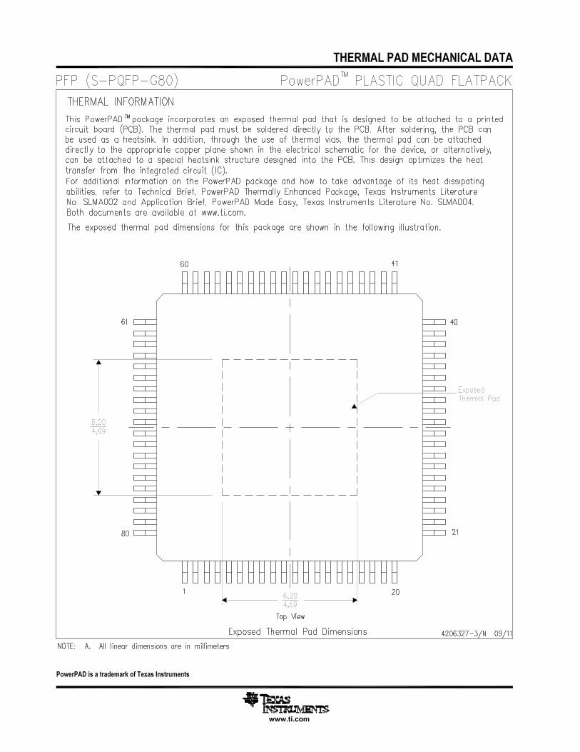
For more information, refer to TI application note PowerPAD™ Thermally Enhanced package, TI literaturenumber SLMA002.
ELECTRICAL CHARACTERISTICSover recommended operating conditions
PARAMETER TEST CONDITIONS MIN NOM MAX UNIT
VDD Supply voltage 2.3 2.5 2.7 V
Frequency = 1.25 Gbps, PRBS pattern 280ICC Supply current mA
Frequency = 2.5 Gbps, PRBS pattern 310
Frequency = 1.25 Gbps, PRBS pattern 700
PD Power dissipation Frequency = 2.5 Gbps, PRBS pattern 775 mW
Frequency = 2.6 Gbps, worst case pattern (1) 825
Low Power Mode current TX_CLK Static, VDDA and VDD = Max 1 mA
PLL startup lock time VDD, VDDC = 2.3 V 0.1 0.4 ms
Data acquisition time Frequency = 1.25 Gbps or 2.5 Gbps, K28.5 D16.2 256 nspattern (3 sigma values)
TA Operating free-air temperature –40 85 °C
(1) Worst case pattern is a pattern that creates a maximum transition density on the serial transceiver.
REFERENCE CLOCK (REFCLK)TIMING REQUIREMENTSover recommended operating conditions (unless otherwise noted)
PARAMETER TEST CONDITIONS MIN TYP MAX UNIT
Frequency Minimum data rate Typ–0.01% 100 Typ+0.01% MHz
Frequency Maximum data rate Typ–0.01% 130 Typ+0.01% MHz
Frequency tolerance –100 100 ppm
Duty cycle 40% 50% 60%
Jitter Peak-to-peak 40 ps
© 2008, Texas Instruments Incorporated Submit Documentation Feedback 7
Product Folder Link(s) :TLK2541

TX_CLK
3.6 V
0 V
TXD[0-19] 1.25 V
1.7 V
1.7 V
0.8 V
3.6 V
0 V
0.8 V
TLK2541SLLS779B –JANUARY 2008–REVISED APRIL 2008 www.ti.com
TTL INPUT ELECTRICAL CHARACTERISTICSover recommended operating conditions (unless otherwise noted), TTL signals: TXD[0:19], TX_CLK, LOOPEN, ENABLE,PRBS_EN, PRE , CTRL0, CTRL1, TXRATE, RXRATE, REFCLK, LCKREFN, TESTEN, RXCODE
PARAMETER TEST CONDITIONS MIN TYP MAX UNIT
VIH High-level input voltage See Figure 2 1.7 3.6 V
VIL Low-level input voltage See Figure 2 0.8 V
IIH Input high current VDD = MAX, VIN = 2 V 40 μA
IIL Input low current VDD = MAX, VIN = 0.4 V –40 μA
CI Receiver input capacitance 4.5 pF
tr Rise time, TXD[0..19] 0.8 V to 1.7 V, C = 5 pF, See Figure 2 1 ns
tf Fall time, TX_CLK, TXD[0..19] 1.7 V to 0.8 V, C = 5 pF, See Figure 2 1 ns
tsu TXD[0:19], setup to ↑ TX_CLK See Figure 2 1.5 ns
th TXD[0:19], hold to ↑ TX_CLK See Figure 2 0.5 ns
Figure 2. TTL Data Input Valid Levels for AC Measurements
8 Submit Documentation Feedback © 2008, Texas Instruments Incorporated
Product Folder Link(s) :TLK2541

RX_CLK
RXD[0-19]
TLK2541www.ti.com SLLS779B –JANUARY 2008–REVISED APRIL 2008
TTL OUTPUT SWITCHING CHARACTERISTICSover recommended operating conditions (unless otherwise noted)
PARAMETER TEST CONDITIONS MIN TYP MAX UNIT
VOH High-level output voltage IOH = –1 mA, VDD = MIN 2.10 2.3 V
VOL Low-level output voltage IOL = 1 mA, VDD = MIN GND 0.25 0.5 V
tr(slew) Slew rate (rising), magnitude of RX_CLK, 0.8 V to 2 V, C = 5 pF, See Figure 3 0.5 V/nsRXD[0:19]
tf(slew) Slew rate (falling), magnitude of RX_CLK, 0.8 V to 2 V, C = 5 pF, See Figure 3 0.5 V/nsRXD[0:19]
50% voltage swing, TX_CLK = 100 MHz, 2.5See Figure 3
tsu RXD[0:19] setup to ↑ RX_CLK ns50% voltage swing, TX_CLK = 130 MHz, 2.5See Figure 3
50% voltage swing, TX_CLK = 100 MHz, 1.5See Figure 3
th RXD[0:19] hold to ↑ RX_CLK ns50% voltage swing, TX_CLK = 130 MHz, 1.5See Figure 3
Duty Cycle, RX_CLK See Figure 3 45% 50% 55%
Figure 3. TTL Data Output Valid Levels for AC Measurements
© 2008, Texas Instruments Incorporated Submit Documentation Feedback 9
Product Folder Link(s) :TLK2541

TLK2541SLLS779B –JANUARY 2008–REVISED APRIL 2008 www.ti.com
TRANSMITTER/RECEIVER CHARACTERISTICSPARAMETER TEST CONDITIONS MIN NOM MAX UNIT
Rt = 50Ω, PREM = high, dc-coupled, See 750 913 1075Figure 4Preemphasis VOD, direct,VOD(p) mVVOD(p) = |VTXP – VTXN| Rt = 50Ω, PREM = low, dc-coupled, See 700 850 1000Figure 4
Rt = 50Ω, PREM = high, dc-coupled, See 1500 1825 2150Figure 4Differential peak-to-peak output voltageVOD(pp_p) mVPPwith preemphasis Rt = 50Ω, PREM = low, dc-coupled, See 1400 1700 2000Figure 4
VOD(d) Deemphais output voltage, 500 600 800 mVRt = 50Ω, dc-coupled, See Figure 4|VTXP–VTXN|
VOD(pp_d) Differential, peak-to-peak output 1000 1300 1600 mVPPRt = 50Ω, dc-coupled, See Figure 4voltage with deemphasis
V(cmt) Transmit common mode voltage range, 1000 1250 1400 mVRt = 50Ω, See Figure 4(VTXP + VTXN)/2
Receiver input voltage differential,VID 200 1600 mV|VRXP – VRXN|
Receiver common mode voltage range,V(cmr) 1000 1250 2250 mV(VRXP + VRXN)/2
Ci Receiver input capacitance 2 pF
Differential output jitter at 2.5 Gbps, Random*12 + deterministic, Based on K28.5/K28.5 .32patternSerial data total jitter (peak-to-peak) UI (1)
Differential output jitter at 1.25 Gbps, 0.19Random*12 + deterministic, PRBS Pattern
Serial data total jitter (Random) Random Jitter (RMS) .016 UI
Differential output signal rise, fall timett, tf RL = 50Ω, CL = 5 pF, See Figure 4 150 ps(20% to 80%)
Differential input jitter, random + .75Jitter tolerance, Total jitter at serial deterministic, PRBS pattern at zero crossing UIinput at 1.25 Gbps
Jitter tolerance, Deterministic jitter at Differential input jitter, deterministic, PRBS .462 UIserial input pattern at zero crossing at 1.25 Gbps
Differential input jitter, random + .60Jitter tolerance, Total jitter at serial deterministic, PRBS pattern at zero crossing UIinput at 2.5 Gbps
Jitter tolerance, Deterministic jitter at Differential input jitter, deterministic, PRBS .37 UIserial input pattern at zero crossing at 2.5 Gbps
td(Tx latency) Tx latency with Coding Off See Figure 6 50 106bits
Tx latency with Coding On 70 126
td(Rx latency) Rx latency for Full Rate See Figure 9 81 100bits
Rx latency for Half Rate 69 83
(1) UI is the time interval of one serialized bit.
Figure 4. Differential and Common-Mode Output Voltage Definitions
10 Submit Documentation Feedback © 2008, Texas Instruments Incorporated
Product Folder Link(s) :TLK2541

TX_CLK
TXD[0-19]
TLK2541www.ti.com SLLS779B –JANUARY 2008–REVISED APRIL 2008
DETAILED DESCRIPTION
TRANSMIT INTERFACE
The TLK2541 offers four modes of operation for the transmit data path. The TLK2541 can operate as a 10 bitSERDES at 10 times the rate of REFCLK or as a 20 bit SERDES at 20 times the rate of REFCLK. At either rate,the data may be serialized exactly as presented on the parallel bus or it may be coded into 8B/10B data codesby way on an integrated 8B/10B encoder.
TRANSMIT DATA BUS
At full data rate, The transmitter portion registers valid incoming 20-bit wide data (TXD[0:19]) on the rising edgeof the TX_CLK. The data is then serialized and transmitted sequentially over the differential high-speed I/Ochannel. The clock multiplier multiplies the reference clock (REFCLK) by a factor of 10 times, creating a bit clock.This internal bit clock is fed to the parallel-to-serial shift register which transmits data on both the rising andfalling edges of the internal bit clock, providing a serial data rate that is 20 times the input clock. Data istransmitted LSB TXD[0] first. If the 8B/10B encoder is enabled, the data is latched as 16 bits of data plus two bitsof control. The lower order byte is latched on TXD[0:7] and the higher order byte is latched on TXD[8:15]. BitTXD[16] controls whether the lower order byte is coded as a Dx.y data word or a Kx.y control word. Bit TXD[17]controls whether the higher order byte is coded as a Dx.y data word or a Kx.y control word. Bits TXD[18] andTXD[19] are ignored.
At half data rate, The transmitter portion registers valid incoming 10-bit wide data (TXD[0:9]) on the rising edge ofthe TX_CLK. The data is then serialized and transmitted sequentially over the differential high-speed I/Ochannel. Bits TXD[10:19] are ignored. The clock multiplier multiplies the reference clock (REFCLK) by a factor of5 times, creating a bit clock. This internal bit clock is fed to the parallel-to-serial shift register which transmits dataon both the rising and falling edges of the bit clock, providing a serial data rate that is 10 times the input clock.Data is transmitted LSB (TXD[0]) first. If the 8B/10B encoder is enabled, the data is latched as 8 bits of data plusone bit of control. The lower order byte is latched on TXD[0:7]. Bit TXD[16] controls whether the lower order byteis coded as a Dx.y data word or a Kx.y control word. Bits TXD[8:15] and TXD[17:19] are ignored. The data andclock signals must be properly aligned as shown in Figure 5. Detailed timing information can be found in theelectrical characteristics table.
Figure 5. Transmit Timing Waveform
Transmit Rate Select
The TLK2541 has two ranges of operation. The TLK2541 may be used to serialize 20 bits of data at a data rateof 20 times the reference clock, or the TLK2541 may be used to serialize 10 bits of data at a rate of 10 times thereference clock. In either case, the reference clock must be in the range of 100 to 130 MHz, allowing theTLK2541 to be used as a 10-bit serializer at a rate of 1 to 1.3 Gbps or as a 20-bit serializer at a rate of 2 to 2.6Gbps. The control pin TXRATE selects the range of operation for the TLK2541 serializer.
When TXRATE is low, the TLK2541 serializes the 10 bit data on TXD[0:9] at a rate of 10 times the referenceclock. Bits TXD[10:19] is ignored. If the 8B/10B encoder is enabled, then bits TXD[0:7] is encoded into a 10 bitcode word and bit TXD[16] controls whether the code is a Dx.y code if TXD[16] is low or a Kx.y code if TXD[16]is high. Bit TXD[9] is ignored.
© 2008, Texas Instruments Incorporated Submit Documentation Feedback 11
Product Folder Link(s) :TLK2541

TXD[0-19] Parallel Word to Transmit
TX_CLK
TLK2541SLLS779B –JANUARY 2008–REVISED APRIL 2008 www.ti.com
When TXRATE is high, the TLK2541 serializes the 20 bit data on TXD[0:19] at a rate of 20 times the referenceclock. Bit TXD[0] is the first bit serialized. If the 8B/10B encoders are enabled, then bits TXD[0:7] is encoded intothe lower order 10 bit code word and bits TXD[8:15] is encoded into the higher order 10 bit code word. The lowerorder code word is serialized first. Bit TXD[16] controls whether the lower order code is a Dx.y code if TXD[16] islow or a Kx.y code if TXD[16] is high. Bit TXD[17] controls whether the higher order code is a Dx.y code ifTXD[17] is low or a Kx.y code if TXD[17] is high. Bits TXD[18] and TXD[19] is ignored.
When TXRATE is high, it is expected (but not required) that a K28.5 code such as that used in a GigabitEthernet IDLE or a FibreChannel ordered set be present on the lower order byte. This is because at the higherdata rate the parallel bus is two bytes wide, and if the receiver is also a TLK2541 with a two-byte wide parallelbus then the receiver must determine which byte to output on the lower order byte of the receive parallel bus.The TLK2541 receiver expects the K28.5 code to be present on the lower order byte and thus the receiverchooses a 20 bit deserialization boundary such that the K28.5 is present on the lower order byte.
TRANSMISSION LATENCY
The data transmission latency of the TLK2541 is defined as the delay from the initial 20-bit word load to theserial transmission of bit 0. The transmit latency is fixed once the link is established. However, due to siliconprocess variations and implementation variables such as supply voltage and temperature, the exact delay varies.The minimum transmit latency td(Tx latency) is 50 bit times; the maximum is 86 bit times when 8b/10b coding is off.The minimum transmit latency td(Tx latency) is 70 bit times; the maximum is 106 bit times when 8b/10b coding is on.Figure 6 illustrates the timing relationship between the transmit data bus, the TX_CLK, and the serial transmitterminals.
Figure 6. Transmission Latency
Optional 8-BIT/10-BIT ENCODER
All true serial interfaces require a method of encoding to insure minimum transition density so that the receivingPLL has a minimal number of transitions to stay locked on. The encoding scheme maintains the signal dcbalance by keeping the number of ones and zeros the same. This provides good transition density for clockrecovery and improves error checking. The TLK2541 uses the 8-bit/10-bit encoding algorithm that is used byfibre channel and gigabit ethernet. This is transparent to the user, as the TLK2541 internally encodes anddecodes the data such that the user reads and writes actual 16-bit data.
The 8-bit/10-bit encoder converts 8-bit wide data to a 10-bit wide encoded data character to improve itstransmission characteristics. Since the TLK2541 is a 16-bit wide interface, the data is split into two 8-bit widebytes for encoding. Each byte is fed into a separate encoder. The encoding is dependent upon two additionalinput signals are presented on pins TXD[16] and TXD[17]. See Table 3.
12 Submit Documentation Feedback © 2008, Texas Instruments Incorporated
Product Folder Link(s) :TLK2541

TLK2541www.ti.com SLLS779B –JANUARY 2008–REVISED APRIL 2008
Table 3. Transmit Data Controls
TXD[16] TXD[17] 16 BIT PARALLEL INPUT FULL RATE WITH 8B/10B CODING
0 0 Valid data on TXD[0:7], Valid data TXD[8:15]
0 1 Valid data on TXD[0:7], K code on TXD[8:15]
1 0 K code on TXD[0:7], Valid data on TXD[8:15]
1 1 K code on TXD[0:7], K code on TXD[8:15]
TXD[16] 8 BIT PARALLEL INPUT HALF RATE WITH 8B/10B CODING
0 Valid data on TXD[0:7]
1 K code on TXD[0:7]
8B/10B Bypass Mode
When control pin CTRL0 and CTRL1 are both held low, the TLK2541 will bypass the integrated 8B/10B encodelogic and will serialize the parallel data as it is presented to the parallel bus without coding or modification. Datais serialized least-significant bit first, so bit TXD[0] is the first bit to be transmitted and bit TXD[19] is the last bittransmitted. For all other combinations of CTRL0 and CTRL1, the data path includes the integrated 8B/10Bencode logic. In this mode, bits TXD[0:7] are presented to the lower order encoder, and bit TXD[16] controlswhether this byte is coded as Dx.y or as Kx.y. If TXD[16] is low, then the data is coded as Dx.y. If TXD[16] ishigh, then the data is coded as Kx.y. Bits TXD[8:15] are presented to the higher order encoder, and bit TXD[17]controls whether the data is coded as Dx.y or Kx.y. When TXD[16] or TXD[17] are used to generate Dx.y codes,all possible combinations of the data codes are valid. However, there are only 12 valid Kx.y codes defined by the8B/10B coding definition. To generate one of these valid K codes, the proper data bit combination must bepresented on the data bus. For example, to generate a K28.5 on the lower order byte, bit TXD[16] is set to logic‘1’ and bits TXD[0:7] are set to ‘10111100’. If the K control bit is set while the data bus is set for an undefinedKx.y code (such as K0.9), then the output of the encoder is undefined and not specified to be valid. When eitherCTRL0 or CTRL1 are set to logic ‘1’, data presented on the parallel bus TDX[0:17] is presented to the 8B/10Bencoders. TXD[18] and TXD[19] are ignored. When both CTRL0 and CTL1 are set to logic ‘1’ the data presentedon the TXD[0:17] bus is encoded and serialized, allowing the use of the TLK2541 for proprietary protocols builtaround the 8B/10B coding standard. For Ethernet or FibreChannel protocols, the Gigabit Ethernet orFibreChannel modes may be better suited for the application.
Gigabit Ethernet IDLE Correction Mode
The IDLE pattern described in the IEEE802.3 clause 36 specification requires the IDLE pattern to be generatedas either K28.5 D5.6 or as K28.5 D16.2 depending on the state of the 8B/10B current running disparity at thetime that the IDLE pattern is sent. If the integrated 8B/10B encoders are used, then there is no way for the hostdevice controlling the TLK2541 TXD[0:19] bus to know whether to send the D5.6 code or the D16.2 code on theupper order byte. If the TLK2541 is to be used to generate valid Ethernet IDLE patterns while using the on board8b/10b encoder, then the Gigabit Ethernet IDLE Correction mode should be enabled. In this mode, a K28.5D16.2 idle may be presented to the transmit parallel bus for all idles, and the TLK2541 substitutes a D5.6 inplace of the D16.2 on those occasions where the current running disparity requires that a K28.5 D5.6 is theproper IDLE to be generated. This mode is enabled when CTRL0 is 0 and CTRL1 is high.
FibreChannel End Of Frame Correction Mode
The EOF pattern described in the ANSI FC-PH FibreChannel specification requires the EOF pattern to begenerated as either K28.5 D21.4 D21.x D21.x or as K28.5 D21.5 D21.× D21.x depending on the state of the8B/10B current running disparity at the time that the EOF pattern is sent. If the integrated 8B/10B encoders areused, then there is no way for the host device controlling the TLK2541 TXD[0:19] bus to know whether to sendone EOF code or the other EOF code. If the TLK2541 is to be used to generate valid FibreChannel EOF patternswhile using the on board 8b/10b encoder then the FibreChannel EOF correction mode should be enabled. In thismode, a K28.5 D21.4 D21.x D21.x EOF is presented to the transmit parallel bus for all EOF ordered sets, andthe TLK2541 substitutes a D21.5 in place of the D21.4 on those occasions where a K28.5 D21.5 D21.× D21.× isthe proper EOF to be generated. This mode is enabled when CTRL0 is 1 and CTRL1 is 0. The EOF correctionmode also corrects the EOF-invalid ordered sets by correcting a K28.5 D10.5 D21.× D21.× ordered set to be aK28.5 D10.4 D21.× D21.× ordered set when necessary.
© 2008, Texas Instruments Incorporated Submit Documentation Feedback 13
Product Folder Link(s) :TLK2541

TLK2541SLLS779B –JANUARY 2008–REVISED APRIL 2008 www.ti.com
PRBS Generator
The TLK2541 has a built-in 27-1 PRBS (pseudo random bit stream) function. When the PRBSEN terminal isforced high, the PRBS test is enabled. A PRBS is generated and fed into the 10-bit parallel-to-serial converterinput register. Data from the normal input source is ignored during the PRBS mode. The PRBS pattern is thenfed through the transmit circuitry as if it were normal data and sent out to the transmitter. The output can be sentto a BERT (bit error rate tester), the receiver of another TLK2541, or looped back to the receive input. Since thePRBS is not really random but a predetermined sequence of ones and zeroes, the data can be captured andchecked for errors by a BERT.
Parallel-to-Serial
The parallel-to-serial shift register takes in the 20-bit wide data word multiplexed from the two parallel 8-bit/10-bitencoders and converts it to a serial stream. The shift register is clocked on both the rising and falling edge of theinternally generated bit clock, which is 10 times the REFCLK input frequency. The LSB (TXD[0]) is transmittedfirst.
High-Speed Data Output
The high-speed data output driver consists of a voltage mode logic (VML) differential pair optimized for a 50-Ωimpedance environment. The magnitude of the differential pair signal swing is compatible with pseudo emittercoupled logic (PECL) levels when ac-coupled. The line can be directly-coupled or ac-coupled. See Figure 11 andFigure 12 for termination details. The outputs also provide preemphasis to compensate for ac loss when driving acable or PCB backplane trace over a long distance (see Figure 7). The level of pre-emphasis is controlled byPRE as shown in Table 4.
Table 4. Programmable Pre-emphasis
PRE PRE-EMPHASIS LEVEL(%)VOD(P), VOD(D)
(1)
0 5%
1 20%
(1) VOD(p) : Voltage swing when there is a transition in the datastream
Figure 7. Output Voltage Under Pre-emphasis VOD(d): Voltage swing when there is no transition in the data(|VTXP–VTXN|) stream.
RECEIVE INTERFACE
The receiver portion of the TLK2541 accepts 8-bit/10-bit encoded differential serial data. The interpolator andclock recovery circuit locks to the data stream and extract the bit rate clock. This recovered clock is used toretime the input data stream. The recovered clock is divided down to output a receive word clock that is outputon RX_CLK. The parallel data is presented on the parallel output bus according to four modes of operation. TheTLK2541 can operate as a 10 bit SERDES at 10 times the rate of REFCLK or as a 20 bit SERDES at 20 timesthe rate of REFCLK. At either rate, the data may be deserialized, byte aligned and output exactly as it iscaptured from the serial inputs or it may be decoded into data bytes by way on an integrated 8B/10B decoder.
Receive Data Bus
At full data rate, the receiver portion locks to an incoming serial data stream and deserializes the data into 20-bitwide data words and outputs them on RXD[0:19] along with the RX_CLK. RX_CLK is aligned with the rising edgein the center of the output data word. The first data bit received is output on RXD[0]. If the 8B/10B decoder isenabled, the data is output as 16 bits of data plus two bits of status. The lower order byte is output on RXD[0:7]and the higher order byte is output on RXD[8:15]. Bit RXD[16] indicates whether the lower order byte wasdecoded as a Dx.y data word or a Kx.y control word. Bit RXD[17] indicates whether the higher order byte wasdecoded as a Dx.y data word or a Kx.y control word. Bits RXD[18] and RTXD[19] are high impedance.
At half data rate, the receiver portion locks to an incoming serial data stream and deserializes the data into 10-bitwide data words and outputs them on RXD[0:9] along with the RX_CLK. RX_CLK is aligned with the rising edge
14 Submit Documentation Feedback © 2008, Texas Instruments Incorporated
Product Folder Link(s) :TLK2541

RX_CLK
RXD[0-19]
RXD[0-19]
RX_CLK
Decoded Parallel Word
TLK2541www.ti.com SLLS779B –JANUARY 2008–REVISED APRIL 2008
in the center of the output data word. The first data bit received is output on RXD[0]. If the 8B/10B encoder isenabled, the data is output as 8 bits of data plus one bit of status. The lower order byte is output on RXD[0:7]. BitRXD[16] indicates whether the lower order byte was decoded as a Dx.y data word or a Kx.y control word. BitsRXD[8:15] and RXD[17:19] and are high impedance The data and clock signals are aligned as shown inFigure 8. Detailed timing information can be found in the switching characteristics table.
Figure 8. Receive Timing Waveform
Data Reception Latency
The serial-to-parallel data receive latency is the time from when the first bit arrives at the receiver until it is outputin the aligned parallel word. The receive latency is fixed once the link is established. However, due to siliconprocess variations and implementation variables such as supply voltage and temperature, the exact delay varies.The minimum receive latency td(Rx latency) is 81 bit times; the maximum is 93 bit times for full rate operation. Theminimum receive latency td(Rx latency) is 69 bit times; the maximum is 81 bit times for half rate operation. Figure 9illustrates the timing relationship between the serial receive terminals, the recovered word clock (RX_CLK), andthe receive data bus.
Figure 9. Receiver Latency
Serial-to-Parallel
Serial data is received on the RXP and RXN terminals. The interpolator and clock recovery circuit locks to thedata stream if the clock to be recovered is within 200 PPM of the internally generated bit rate clock. Therecovered clock is used to retime the input data stream. The serial data is then clocked into the serial-to-parallelshift registers. The 10-bit wide parallel data is then multiplexed and fed into two separate 8-bit/10-bit decoderswhere the data is then synchronized to the incoming data stream word boundary by detection of the comma8-bit/10-bit synchronization pattern.
Comma Detect and Optional 8-Bit/10-Bit Decoding
The TLK2541 has two parallel 8-bit/10-bit decode circuits. Each 8-bit/10-bit decoder converts 10 bit encodeddata (half of the 20-bit received word) back into 8 bits. The comma detect circuit is designed to provide for bytesynchronization to an 8-bit/10-bit transmission code. When parallel data is clocked into a parallel to serialconverter, the byte boundary that was associated with the parallel data is now lost in the serialization of the data.When the serial data is received and converted to parallel format again, a method is needed to recognize thebyte boundary. This is accomplished through the use of a synchronization pattern. This is a unique pattern of 1'sand 0's that either cannot occur as part of valid data, or is a pattern that repeats at defined intervals. The
© 2008, Texas Instruments Incorporated Submit Documentation Feedback 15
Product Folder Link(s) :TLK2541

TLK2541SLLS779B –JANUARY 2008–REVISED APRIL 2008 www.ti.com
8-bit/10-bit encoding contains a character called the comma (b0011111 or b1100000), which is used by thecomma detect circuit on the TLK2541 to align the received serial data back to its original byte boundary. Thedecoder detects the comma, generating a synchronization signal aligning the data to their 10-bit boundaries fordecoding; the comma is mapped into the LSB. The decoder then converts the data back into 8-bit data. Theoutput from the two decoders is latched into the 16-bit register synchronized to the recovered parallel data clock(RX_CLK) and output valid on the rising edge of the RX_CLK.
Since the TLK2541 must determine which byte of data belongs on the lower order byte of the parallel output bus,the K code that contains a comma pattern is chosen to be output on the lower order byte. Protocols such asGigabit Ethernet or Fibre Channel are defined such that the K28.5 is only present on 20 or 40 bit boundaries.
NOTEThe TLK2541 only achieves byte alignment on the 0011111 comma.
Decoding provides two additional status signals, RXD[16] and pin RXD[17]. When RXD[16] is high , an8-bit/10-bit K code was received and the specific K code is presented on the data bits RXD[0:7]; otherwise, an8-bit/10-bit D code was received. When RXD[17] is high, an 8-bit/10-bit K code was received and the specificK-code is presented on data bits RXD[8:15]; otherwise, an 8-bit/10-bit D code was received (see Table 5). Thevalid K codes the TLK2541 decodes are provided in Table 6. An error detected on either byte, including K codesnot in Table 6, causes that byte only to indicate a K0.0 code on the RXD[16] or RXD[17] and associated datapins, where K0.0 is known to be an invalid 8-bit/10-bit code.
8B/10B Decode Bypass
When control pin RXCODE is held low, the TLK2541 will bypass the integrated 8B/10B decode logic and willpresent the raw 20 bit deserialized data on the output pins RXD[0:19]. If RXCODE is high, then the deserializeddata will be decoded by the integrated 8B/10B decoder and the decoded data will be output on the output pinsRXD[0:19].
RX Rate Select
The TLK2541 receiver has two ranges of operation. The TLK2541 may be used to deserialize 20 bits of data at adata rate of 20 times the reference clock, or the TLK2541 may be used to deserialize 10 bits of data at a rate of10 times the reference clock. In either case, the reference clock must be in the range of 100 to 130 MHz,allowing the TLK2541 to be used as a 10-bit deserializer at a rate of 1 to 1.3 Gbps or as a 20-bit deserializer at arate of 2 to 2.6 Gbps. The control pin RXRATE selects the range of operation for the TLK2541 deserializer. Therecovered byte clock is always in the range of 100 to 130 MHz. The data rate range for the TLK2541 receivermay be selected independently of the TLK2541 transmitter. The TLK2541 may receive a data stream that is halfthe rate of the transmitted data stream, or twice that of the transmitted data stream, or the same as thetransmitted data stream. At whatever data rate is chosen for the receiver, the Clock/Data Recovery (CDR)function in the TLK2541 receiver may lock to and track an incoming data stream that is as much as ± 200 ppmaway from the nominal data rate as referenced by the REFCLK to the TLK2541.
When RXRATE is low, the TLK2541 deserializes the data stream into a 10 bit data byte and output it onRXD[0:9]. Bits RXD[10:19] are high-impedance. If the 8B/10B decoder is enabled, then the 10 bit deserializeddata is decoded and output on bits RXD[0:7], and bit RXD[16] indicates whether the code is a Dx.y code ifRXD[16] is low or a Kx.y code if RXD[16] is high. Bits RXD[8:15] and RXD[17:19] are high-impedance.
When RXRATE is high, the TLK2541 deserializes the data stream into a 20 bit data word and output it on bitsRXD[0:19]. Bit RXD[0] is the first bit received. If the 8B/10B decoders are enabled, then bits RXD[0:7] outputs thelower order 10 bit deserialized code word and bits RXD[8:15] output the higher order 10 bit deserialized codeword. The lower order code word is the first byte received. Bit RXD[16] indicates whether the lower order code isa Dx.y code if RXD[16] is low or a Kx.y code if RXD[16] is high. Bit RXD[17] indicates whether the higher ordercode is a Dx.y code if RXD[17] is low or a Kx.y code if RXD[17] is high. Bits RXD[18] and RXD[19] are highimpedance.
When RXRATE is high, a K28.5 code such as that used in a Gigabit Ethernet IDLE or a FibreChannel orderedset is output on the lower order byte. This is because at the higher data rate the parallel bus is two bytes wide,and the receiver must determine which byte to output on the lower order byte of the receive parallel bus. TheTLK2541 receiver expects the K28.5 code to be present on the lower order byte and thus the receiver chooses a20 bit deserialization boundary such that the K28.5 is present on the lower order byte.
16 Submit Documentation Feedback © 2008, Texas Instruments Incorporated
Product Folder Link(s) :TLK2541

TLK2541www.ti.com SLLS779B –JANUARY 2008–REVISED APRIL 2008
Table 5. Receive Status Signals
RXD[16] RXD[17] DECODED 20 BIT OUTPUT FULL RATE WITH 8B/10B CODING
0 0 Valid data on RXD[0:7], Valid data RXD[8:15]
0 1 Valid data on RXD[0:7], K code on RXD[8:15]
1 0 K code on RXD[0:7], Valid data on RXD[8:15]
1 1 K code on RXD[0:7], K code on RXD[8:15]
RXD[16] DECODED 20 BIT OUTPUT HALF RATE WITH 8B/10B CODING
0 Valid data on RXD[0:7]
1 K code on RXD[0:7]
Table 6. Valid K Characters
RECEIVE DATA BUSK CHARACTER (RXD[0:7]) OR (RXD[8:15])
K28.0 000 11100
K28.1 (1) 001 11100
K28.2 010 111000
K28.3 011 111000
K28.4 100 11100
K28.5 (1) 101 11100
K28.6 110 111001
K28.7 (1) 111 11100
K23.7 111 101111
K27.7 111 110111
K29.7 111 111011
K30.7 111 111101
(1) Should only be present on RXD[7–0] when in running disparity < 0.
Lock to Reference
When the LCKREFN pin is asserted (active low), the tracking circuitry on the receiver Clock/Data Recovery(CDR) circuit is disabled, and the recovered byte clock becomes a buffered version of REFCLK. If there is not avalid serial data stream while the receiver is attempting to lock onto and track a serial data stream, then it ispossible for the recovered byte clock to drift to a frequency above or below the desired data rate by as much as2000 ppm depending on noise components of the invalid input serial data stream. The assertion of LCKREFN,while there is no valid incoming serial data, would ensure that the recovered byte clock does not drift away fromREFCLK. The use of LCKREFN is not required to help the receiver lock onto incoming serial data, and the use ofLCKREFN does not speed the process of locking onto data once LCKREFN is released.
Power Down Mode
When the reference clock (REFCLK) is held static, the TLK2541 goes into power-down mode. In power-downmode, the serial transmit pins (TXN and TXP) , and the receive data bus pins (RXD[0:19]) go into ahigh-impedance state. When the reference clock begins to toggle at a rate approaching its minimumrecommended operating frequency then the TLK2541 will go through its power-on reset procedure.
PRBS Verification
The TLK2541 also has a built-in BERT function in the receiver side that is enabled by the PRBSEN. It can checkfor errors and report the errors by forcing the PRBSPASS terminal low.
© 2008, Texas Instruments Incorporated Submit Documentation Feedback 17
Product Folder Link(s) :TLK2541

TLK2541SLLS779B –JANUARY 2008–REVISED APRIL 2008 www.ti.com
Reference Clock Input
The reference clock (REFCLK) is an external input clock that sets the rate of the transmitted serial data stream.The reference clock is then multiplied in frequency 10 times to produce the internal serialization bit clock. In fullrate mode, the internal serialization bit clock is frequency-locked to the input clock and used to clock out theserial transmit data on both its rising and falling edges, providing a serial data rate that is 20 times the inputclock.
Operating Frequency Range
The TLK2541 can operate at a serial data rate from 1.0 Gbps to 1.3 Gbps or 2.0 to 2.6 Gbps. To achieve theseserial rates, REFCLK must be within 100 MHz to 130 MHz. The frequency accuracy of REFCLK is expected tobe within 100 PPM of the desired rate. The transmit path data rate will be set by REFCLK and the receive pathdata rate is expected to be within 200 PPM of the transmit path data rate.
Testability
The TLK2541 has a comprehensive suite of built-in self-tests. The loopback function provides for at-speedtesting of the transmit/receive portions of the circuitry. The enable terminal allows for all circuitry to be disabledso that a quiescent current test can be performed. The PRBS function allows for BIST (built-in self-test).
Loopback Testing
The transceiver can provide a self-test function by enabling (LOOPEN) the internal loop-back path. Enabling thisterminal causes serial-transmitted data to be routed internally to the receiver. The parallel data output can becompared to the parallel input data for functional verification. (The external differential output is held in a highimpedance state during the loopback testing.)
Built-In Self-Test (BIST)
The TLK2541 has a BIST function. By combining PRBS with loopback, an effective self-test of all the circuitryrunning at full speed can be realized. The successful completion of the BIST is reported on the PRBSPASSterminal. The PRBS generation and verification can operate at either full rate or half rate, but both PRBSgeneration and verification must be at the same rate or PRBSPASS will report an error condition.
Power-On Reset
Upon application of minimum valid power or upon application of a minimum toggling reference clock, theTLK2541 generates a power-on reset. During the power-on reset the RXD[0:19] and serial output signalterminals go to a high impedance state. The RX_CLK is held low. The length of the power-on reset cycle isdependent upon the input frequency, but is less than 1 ms.
18 Submit Documentation Feedback © 2008, Texas Instruments Incorporated
Product Folder Link(s) :TLK2541

TLK2541www.ti.com SLLS779B –JANUARY 2008–REVISED APRIL 2008
APPLICATION INFORMATION
Figure 10. External Component Interconnection
Figure 11. High-Speed I/O Directly-Coupled Mode
Figure 12. High-Speed I/O AC-Coupled Mode
© 2008, Texas Instruments Incorporated Submit Documentation Feedback 19
Product Folder Link(s) :TLK2541

PACKAGING INFORMATION
Orderable Device Status (1) PackageType
PackageDrawing
Pins PackageQty
Eco Plan (2) Lead/Ball Finish MSL Peak Temp (3)
TLK2541PFP ACTIVE HTQFP PFP 80 96 Green (RoHS &no Sb/Br)
CU NIPDAU Level-3-260C-168 HR
TLK2541PFPG4 ACTIVE HTQFP PFP 80 96 Green (RoHS &no Sb/Br)
CU NIPDAU Level-3-260C-168 HR
TLK2541PFPR ACTIVE HTQFP PFP 80 1000 Green (RoHS &no Sb/Br)
CU NIPDAU Level-3-260C-168 HR
TLK2541PFPRG4 ACTIVE HTQFP PFP 80 1000 Green (RoHS &no Sb/Br)
CU NIPDAU Level-3-260C-168 HR
(1) The marketing status values are defined as follows:ACTIVE: Product device recommended for new designs.LIFEBUY: TI has announced that the device will be discontinued, and a lifetime-buy period is in effect.NRND: Not recommended for new designs. Device is in production to support existing customers, but TI does not recommend using this part ina new design.PREVIEW: Device has been announced but is not in production. Samples may or may not be available.OBSOLETE: TI has discontinued the production of the device.
(2) Eco Plan - The planned eco-friendly classification: Pb-Free (RoHS), Pb-Free (RoHS Exempt), or Green (RoHS & no Sb/Br) - please checkhttp://www.ti.com/productcontent for the latest availability information and additional product content details.TBD: The Pb-Free/Green conversion plan has not been defined.Pb-Free (RoHS): TI's terms "Lead-Free" or "Pb-Free" mean semiconductor products that are compatible with the current RoHS requirementsfor all 6 substances, including the requirement that lead not exceed 0.1% by weight in homogeneous materials. Where designed to be solderedat high temperatures, TI Pb-Free products are suitable for use in specified lead-free processes.Pb-Free (RoHS Exempt): This component has a RoHS exemption for either 1) lead-based flip-chip solder bumps used between the die andpackage, or 2) lead-based die adhesive used between the die and leadframe. The component is otherwise considered Pb-Free (RoHScompatible) as defined above.Green (RoHS & no Sb/Br): TI defines "Green" to mean Pb-Free (RoHS compatible), and free of Bromine (Br) and Antimony (Sb) based flameretardants (Br or Sb do not exceed 0.1% by weight in homogeneous material)
(3) MSL, Peak Temp. -- The Moisture Sensitivity Level rating according to the JEDEC industry standard classifications, and peak soldertemperature.
Important Information and Disclaimer:The information provided on this page represents TI's knowledge and belief as of the date that it isprovided. TI bases its knowledge and belief on information provided by third parties, and makes no representation or warranty as to theaccuracy of such information. Efforts are underway to better integrate information from third parties. TI has taken and continues to takereasonable steps to provide representative and accurate information but may not have conducted destructive testing or chemical analysis onincoming materials and chemicals. TI and TI suppliers consider certain information to be proprietary, and thus CAS numbers and other limitedinformation may not be available for release.
In no event shall TI's liability arising out of such information exceed the total purchase price of the TI part(s) at issue in this document sold by TIto Customer on an annual basis.
PACKAGE OPTION ADDENDUM
www.ti.com 11-Jul-2008
Addendum-Page 1

TAPE AND REEL INFORMATION
*All dimensions are nominal
Device PackageType
PackageDrawing
Pins SPQ ReelDiameter
(mm)
ReelWidth
W1 (mm)
A0(mm)
B0(mm)
K0(mm)
P1(mm)
W(mm)
Pin1Quadrant
TLK2541PFPR HTQFP PFP 80 1000 330.0 24.4 15.0 15.0 1.5 20.0 24.0 Q2
PACKAGE MATERIALS INFORMATION
www.ti.com 12-May-2011
Pack Materials-Page 1

*All dimensions are nominal
Device Package Type Package Drawing Pins SPQ Length (mm) Width (mm) Height (mm)
TLK2541PFPR HTQFP PFP 80 1000 346.0 346.0 41.0
PACKAGE MATERIALS INFORMATION
www.ti.com 12-May-2011
Pack Materials-Page 2


IMPORTANT NOTICE
Texas Instruments Incorporated and its subsidiaries (TI) reserve the right to make corrections, modifications, enhancements, improvements,and other changes to its products and services at any time and to discontinue any product or service without notice. Customers shouldobtain the latest relevant information before placing orders and should verify that such information is current and complete. All products aresold subject to TI’s terms and conditions of sale supplied at the time of order acknowledgment.
TI warrants performance of its hardware products to the specifications applicable at the time of sale in accordance with TI’s standardwarranty. Testing and other quality control techniques are used to the extent TI deems necessary to support this warranty. Except wheremandated by government requirements, testing of all parameters of each product is not necessarily performed.
TI assumes no liability for applications assistance or customer product design. Customers are responsible for their products andapplications using TI components. To minimize the risks associated with customer products and applications, customers should provideadequate design and operating safeguards.
TI does not warrant or represent that any license, either express or implied, is granted under any TI patent right, copyright, mask work right,or other TI intellectual property right relating to any combination, machine, or process in which TI products or services are used. Informationpublished by TI regarding third-party products or services does not constitute a license from TI to use such products or services or awarranty or endorsement thereof. Use of such information may require a license from a third party under the patents or other intellectualproperty of the third party, or a license from TI under the patents or other intellectual property of TI.
Reproduction of TI information in TI data books or data sheets is permissible only if reproduction is without alteration and is accompaniedby all associated warranties, conditions, limitations, and notices. Reproduction of this information with alteration is an unfair and deceptivebusiness practice. TI is not responsible or liable for such altered documentation. Information of third parties may be subject to additionalrestrictions.
Resale of TI products or services with statements different from or beyond the parameters stated by TI for that product or service voids allexpress and any implied warranties for the associated TI product or service and is an unfair and deceptive business practice. TI is notresponsible or liable for any such statements.
TI products are not authorized for use in safety-critical applications (such as life support) where a failure of the TI product would reasonablybe expected to cause severe personal injury or death, unless officers of the parties have executed an agreement specifically governingsuch use. Buyers represent that they have all necessary expertise in the safety and regulatory ramifications of their applications, andacknowledge and agree that they are solely responsible for all legal, regulatory and safety-related requirements concerning their productsand any use of TI products in such safety-critical applications, notwithstanding any applications-related information or support that may beprovided by TI. Further, Buyers must fully indemnify TI and its representatives against any damages arising out of the use of TI products insuch safety-critical applications.
TI products are neither designed nor intended for use in military/aerospace applications or environments unless the TI products arespecifically designated by TI as military-grade or "enhanced plastic." Only products designated by TI as military-grade meet militaryspecifications. Buyers acknowledge and agree that any such use of TI products which TI has not designated as military-grade is solely atthe Buyer's risk, and that they are solely responsible for compliance with all legal and regulatory requirements in connection with such use.
TI products are neither designed nor intended for use in automotive applications or environments unless the specific TI products aredesignated by TI as compliant with ISO/TS 16949 requirements. Buyers acknowledge and agree that, if they use any non-designatedproducts in automotive applications, TI will not be responsible for any failure to meet such requirements.
Following are URLs where you can obtain information on other Texas Instruments products and application solutions:
Products Applications
Audio www.ti.com/audio Communications and Telecom www.ti.com/communications
Amplifiers amplifier.ti.com Computers and Peripherals www.ti.com/computers
Data Converters dataconverter.ti.com Consumer Electronics www.ti.com/consumer-apps
DLP® Products www.dlp.com Energy and Lighting www.ti.com/energy
DSP dsp.ti.com Industrial www.ti.com/industrial
Clocks and Timers www.ti.com/clocks Medical www.ti.com/medical
Interface interface.ti.com Security www.ti.com/security
Logic logic.ti.com Space, Avionics and Defense www.ti.com/space-avionics-defense
Power Mgmt power.ti.com Transportation and Automotive www.ti.com/automotive
Microcontrollers microcontroller.ti.com Video and Imaging www.ti.com/video
RFID www.ti-rfid.com
OMAP Mobile Processors www.ti.com/omap
Wireless Connctivity www.ti.com/wirelessconnectivity
TI E2E Community Home Page e2e.ti.com
Mailing Address: Texas Instruments, Post Office Box 655303, Dallas, Texas 75265Copyright © 2011, Texas Instruments Incorporated