Single-layer crystalline phases of antimony: Antimonenes
11
See discussions, stats, and author profiles for this publication at: https://www.researchgate.net/publication/280244769 Single-layer crystalline phases of antimony: Antimonenes ARTICLE in PHYSICAL REVIEW B · JUNE 2015 Impact Factor: 3.74 · DOI: 10.1103/PhysRevB.91.235446 CITATIONS 2 READS 49 3 AUTHORS: Olcay uzengi akturk Adnan Menderes University 14 PUBLICATIONS 83 CITATIONS SEE PROFILE Ongun Ozcelik Princeton University 27 PUBLICATIONS 199 CITATIONS SEE PROFILE Salim Ciraci Bilkent University 306 PUBLICATIONS 11,028 CITATIONS SEE PROFILE Available from: Ongun Ozcelik Retrieved on: 08 January 2016
Transcript of Single-layer crystalline phases of antimony: Antimonenes
Seediscussions,stats,andauthorprofilesforthispublicationat:https://www.researchgate.net/publication/280244769
Single-layercrystallinephasesofantimony:Antimonenes
ARTICLEinPHYSICALREVIEWB·JUNE2015
ImpactFactor:3.74·DOI:10.1103/PhysRevB.91.235446
CITATIONS
2
READS
49
3AUTHORS:
Olcayuzengiakturk
AdnanMenderesUniversity
14PUBLICATIONS83CITATIONS
SEEPROFILE
OngunOzcelik
PrincetonUniversity
27PUBLICATIONS199CITATIONS
SEEPROFILE
SalimCiraci
BilkentUniversity
306PUBLICATIONS11,028CITATIONS
SEEPROFILE
Availablefrom:OngunOzcelik
Retrievedon:08January2016
PHYSICAL REVIEW B 91, 235446 (2015)
Single-layer crystalline phases of antimony: Antimonenes
O. Uzengi Akturk,1 V. Ongun Ozcelik,2,3 and S. Ciraci4,*
1Department of Physics, Adnan Menderes University, 09100 Aydın, Turkey2UNAM-National Nanotechnology Research Center, Bilkent University, 06800 Ankara, Turkey3Institute of Materials Science and Nanotechnology, Bilkent University, 06800 Ankara, Turkey
4Department of Physics, Bilkent University, 06800 Ankara, Turkey(Received 24 April 2015; revised manuscript received 6 June 2015; published 25 June 2015)
The pseudolayered character of 3D bulk crystals of antimony has led us to predict its 2D single-layer crystallinephase named antimonene in a buckled honeycomb structure like silicene. Sb atoms also form an asymmetricwashboard structure like black phospherene. Based on an extensive analysis comprising ab initio phonon andfinite-temperature molecular dynamics calculations, we show that these two single-layer phases are robust andcan remain stable at high temperatures. They are nonmagnetic semiconductors with band gaps ranging from0.3 eV to 1.5 eV, and are suitable for 2D electronic applications. The washboard antimonene displays stronglydirectional mechanical properties, which may give rise to a strong influence of strain on the electronic properties.Single-layer antimonene phases form bilayer and trilayer structures with wide interlayer spacings. In multilayers,this spacing is reduced and eventually the structure changes to 3D pseudolayered bulk crystals. The zigzag andarmchair nanoribbons of the antimonene phases have fundamental band gaps derived from reconstructed edgestates and display a diversity of magnetic and electronic properties depending on their width and edge geometry.Their band gaps are tunable with the widths of the nanoribbons. When grown on substrates, such as germaneneor Ge(111), the buckled antimonene attains a significant influence of substrates.
DOI: 10.1103/PhysRevB.91.235446 PACS number(s): 31.15.A−, 81.05.Zx, 68.65.−k, 81.05.ue
I. INTRODUCTION
The search for the contender of graphene has led to theprediction/synthesis of new single-layer, crystalline nanos-tructures and their van der Waals heterostructures, which donot exist in nature. Silicene, germanene, and stanene, namelygraphene analogs of group IV elements [1–5]; h-BN analogsof group IV-IV, III-V, and II-VI compounds [6]; graphyne[7–9]; and the auxetic piezoelectric 2D material silicatenewith negative Poisson’s ratio [10,11], have been activelystudied. Additionally, transition-metal dichalcogenides haveproven to be superior to graphene in specific optoelectronicapplications [12–15]. More recently, the fabrication of fieldeffect transistors using micrometer-sized flakes consisting oftwo to three layers of black phosphorus [16] and theoreticalanalysis [17,18] revealing the stability of its single-layerallotropes brought group V elements into the focus.
Our theoretical study exploiting the idea of whether othergroup V elements can form single-layer structures has revealedthat Sb, As, and N atoms can indeed form 2D crystallinestructures like silicene or black phosphorene. This paperreports that 2D, single-layer crystalline phases of antimony,named antimonene, can remain stable. Moreover, their 1Dribbons, bilayers, trilayers, and multilayers are also stable anddisplay electronic and magnetic properties which may lead topotential applications in emerging 2D electronics.
Here we first examined the 3D bulk crystal of Sb havingthe trigonal and hexagonal lattice with the R3-mh spacegroup, which display a pseudolayered atomic configurationas if it were constructed by the stacking of the layers havingbuckled honeycomb structure. Using structure optimizationsbased on the conjugate gradient method we then revealedtwo single-layer phases of Sb, namely buckled antimonene
(B-antimonene or simply B-Sb) similar to silicene andwashboard antimonene (W-antimonene or simply W-Sb)similar to black phospherene. While W-Sb is prone to long-wavelength instability, an asymmetric washboard structure(aW-antimonene or simply aW-Sb) is found to have slightlylower energy. We carried out an extensive analysis to ensurethat B-Sb and aW-Sb single-layer structures are stable aboveroom temperature. We examined the character of their bondingand investigated the effects of vacancy defects. We then char-acterized these phases, their quasi-1D nanoribbons, bilayers,and multilayers by calculating their mechanical, electronic,and magnetic properties. Furthermore we showed how theseproperties deduced for suspended antimonene are modifiedwhen antimonene was grown on substrates like germaneneand Ge(111) surfaces. Our predictions are corroborated by thefabrication of thin antimony films [19–21].
II. METHOD
Our predictions regarding 3D bulk antimony and 2Dsingle-layer antimonene phases, as well as their 1D and 3Dstructures, are obtained from first-principles, pseudopotentialplane wave calculations based on the spin-polarized densityfunctional theory (DFT). We used the generalized gradientapproximation including van der Waals (vdW) correctionsat the DFT-D2 level [22], which was found to be suitablefor layered structures in our earlier tests [23]. Owing to thelocation of the Sb atom in the fifth row of the periodictable, spin-orbit coupling (SOC) is also included in specificcalculations. Similar first-principles DFT studies carried outin the past have been successful in predicting several new2D structures [2,6,10,15], which were subsequently synthe-sized/fabricated. We used projector-augmented wave (PAW)potentials [24] and the exchange-correlation was approximatedby the Perdew-Burke-Ernzerhof (PBE) functional [25]. Whileoptimizing atomic positions using the conjugate gradient
1098-0121/2015/91(23)/235446(10) 235446-1 ©2015 American Physical Society
AKTURK, OZCELIK, AND CIRACI PHYSICAL REVIEW B 91, 235446 (2015)
(CG) method, the energy convergence value between twoconsecutive steps was chosen as 10−5 eV and the maximumHellmann-Feynman force acting on each atom was lessthan 0.02 eV/A. Calculations were carried out using theVASP software [26]. A plane-wave basis set with kineticenergy cutoff of 300 eV was used. The Brillouin zone (BZ)corresponding to the primitive unit cell was sampled by a finegrid [27] of (11 × 11 × 9), (21 × 21 × 1), and (21 × 1 × 1) kpoints for 3D, 2D, and 1D systems, respectively. Both kineticenergy cutoff and k-point sampling values are determinedby performing extensive convergence analyses. For example,increasing their values used in the calculations by 20% resultedin changes in the energies by less than 10−5 eV.
Since the band gaps are underestimated by standard DFT,we also carried out calculations using the screened hybridfunctional, HSE06 method [28]. In addition to ab initio phononcalculations [29], the stability of the optimized structureswas tested at high temperatures by performing ab initio,finite-temperature molecular dynamics (MD) calculations. A
Nose thermostat is used and Newton’s equation of motion isintegrated through the Verlet algorithm with time steps of 2 fs.
III. PSEUDOLAYERED 3D CRYSTAL OF Sb
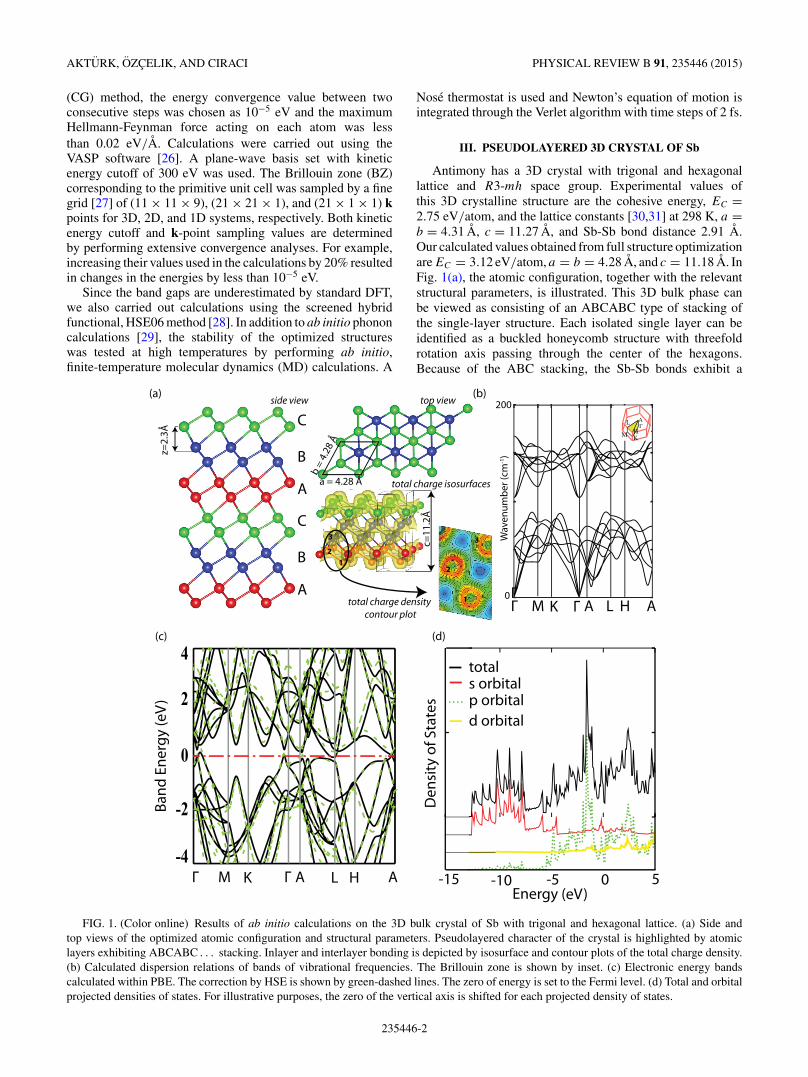
Antimony has a 3D crystal with trigonal and hexagonallattice and R3-mh space group. Experimental values ofthis 3D crystalline structure are the cohesive energy, EC =2.75 eV/atom, and the lattice constants [30,31] at 298 K, a =b = 4.31 A, c = 11.27 A, and Sb-Sb bond distance 2.91 A.Our calculated values obtained from full structure optimizationare EC = 3.12 eV/atom, a = b = 4.28 A, and c = 11.18 A. InFig. 1(a), the atomic configuration, together with the relevantstructural parameters, is illustrated. This 3D bulk phase canbe viewed as consisting of an ABCABC type of stacking ofthe single-layer structure. Each isolated single layer can beidentified as a buckled honeycomb structure with threefoldrotation axis passing through the center of the hexagons.Because of the ABC stacking, the Sb-Sb bonds exhibit a
0
200
Γ M K A L H A
mc( rebmuneva
W1-)
Den
sity
of S
tate
s
totals orbitalp orbitald orbital
A
B
C
A
B
Cweiv potweiv edis
total charge isosurfaces
-10 5-5 0-15Energy (eV)
Γ
(a)
z=2.
3Å
(b)
(d)(c)
12
3
1
2
3
total charge density contour plot
a = 4.28 Å
b =
4.28
Å
c=11
.2Å
-4
-2
0
2
4
Band
Ene
rgy
(eV
)
Γ M K A
Γ
Γ L H A
ΓALHM K
FIG. 1. (Color online) Results of ab initio calculations on the 3D bulk crystal of Sb with trigonal and hexagonal lattice. (a) Side andtop views of the optimized atomic configuration and structural parameters. Pseudolayered character of the crystal is highlighted by atomiclayers exhibiting ABCABC . . . stacking. Inlayer and interlayer bonding is depicted by isosurface and contour plots of the total charge density.(b) Calculated dispersion relations of bands of vibrational frequencies. The Brillouin zone is shown by inset. (c) Electronic energy bandscalculated within PBE. The correction by HSE is shown by green-dashed lines. The zero of energy is set to the Fermi level. (d) Total and orbitalprojected densities of states. For illustrative purposes, the zero of the vertical axis is shifted for each projected density of states.
235446-2
SINGLE-LAYER CRYSTALLINE PHASES OF ANTIMONY: . . . PHYSICAL REVIEW B 91, 235446 (2015)
staggered arrangement in the top view. The smallest interlayerspacing between single layers is z = 2.3 A and hence itallows not only vdW attraction, but also significant chemicalinteraction. This is clarified by the contour plots of the totalcharge density on a plane including two atoms in differentlayers. In this respect, 3D Sb is different from graphite andMoS2, where interlayer binding is mainly vdW attraction.Because of significant interaction between layers we identifythis 3D crystal as pseudolayered. The calculated bands of thevibration frequencies are presented in Fig. 1(b). As shown inFig. 1(c), the highest valence band slightly raises above theFermi level attributing a metallic (semimetallic) character tothe 3D crystal of antimony. Corrections to DFT band energiesusing the HSE06 method confirmed this situation. Metallic(semimetallic) character is attained by coupling betweenadjacent layers of buckled honeycomb structure. The total andorbital projected densities of states (DOS) in Fig. 1(d) showthat 5p-like orbital states dominate the top of the valenceband and the bottom of the conduction band, whereas thelower part of the valence band is derived from 5s orbitals.The pseudolayered character of the 3D Sb crystal has ledus to consider first the 2D single-layer, buckled honeycombstructure of Sb similar to silicene [1,2].
IV. MONOLAYER B-, W-, AND aW-ANTIMONENE
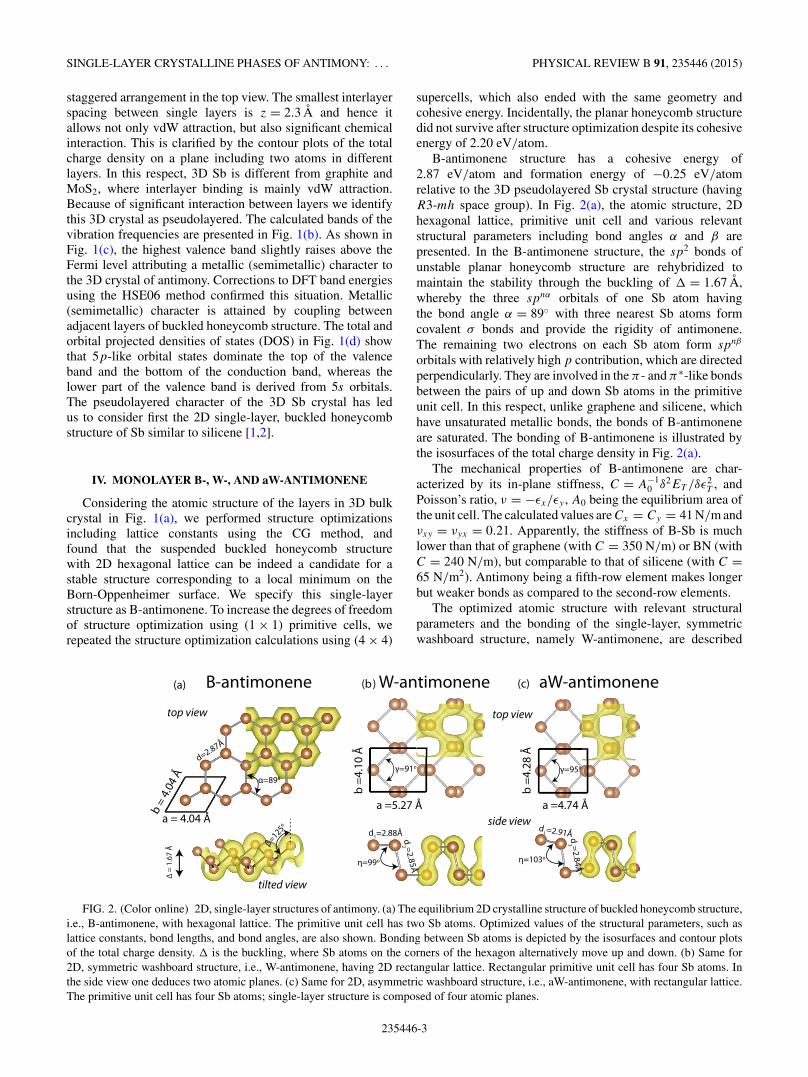
Considering the atomic structure of the layers in 3D bulkcrystal in Fig. 1(a), we performed structure optimizationsincluding lattice constants using the CG method, andfound that the suspended buckled honeycomb structurewith 2D hexagonal lattice can be indeed a candidate for astable structure corresponding to a local minimum on theBorn-Oppenheimer surface. We specify this single-layerstructure as B-antimonene. To increase the degrees of freedomof structure optimization using (1 × 1) primitive cells, werepeated the structure optimization calculations using (4 × 4)
supercells, which also ended with the same geometry andcohesive energy. Incidentally, the planar honeycomb structuredid not survive after structure optimization despite its cohesiveenergy of 2.20 eV/atom.
B-antimonene structure has a cohesive energy of2.87 eV/atom and formation energy of −0.25 eV/atomrelative to the 3D pseudolayered Sb crystal structure (havingR3-mh space group). In Fig. 2(a), the atomic structure, 2Dhexagonal lattice, primitive unit cell and various relevantstructural parameters including bond angles α and β arepresented. In the B-antimonene structure, the sp2 bonds ofunstable planar honeycomb structure are rehybridized tomaintain the stability through the buckling of � = 1.67 A,whereby the three spnα orbitals of one Sb atom havingthe bond angle α = 89◦ with three nearest Sb atoms formcovalent σ bonds and provide the rigidity of antimonene.The remaining two electrons on each Sb atom form spnβ
orbitals with relatively high p contribution, which are directedperpendicularly. They are involved in the π - and π∗-like bondsbetween the pairs of up and down Sb atoms in the primitiveunit cell. In this respect, unlike graphene and silicene, whichhave unsaturated metallic bonds, the bonds of B-antimoneneare saturated. The bonding of B-antimonene is illustrated bythe isosurfaces of the total charge density in Fig. 2(a).
The mechanical properties of B-antimonene are char-acterized by its in-plane stiffness, C = A−1
0 δ2ET /δε2T , and
Poisson’s ratio, ν = −εx/εy , A0 being the equilibrium area ofthe unit cell. The calculated values are Cx = Cy = 41 N/m andνxy = νyx = 0.21. Apparently, the stiffness of B-Sb is muchlower than that of graphene (with C = 350 N/m) or BN (withC = 240 N/m), but comparable to that of silicene (with C =65 N/m2). Antimony being a fifth-row element makes longerbut weaker bonds as compared to the second-row elements.
The optimized atomic structure with relevant structuralparameters and the bonding of the single-layer, symmetricwashboard structure, namely W-antimonene, are described
FIG. 2. (Color online) 2D, single-layer structures of antimony. (a) The equilibrium 2D crystalline structure of buckled honeycomb structure,i.e., B-antimonene, with hexagonal lattice. The primitive unit cell has two Sb atoms. Optimized values of the structural parameters, such aslattice constants, bond lengths, and bond angles, are also shown. Bonding between Sb atoms is depicted by the isosurfaces and contour plotsof the total charge density. � is the buckling, where Sb atoms on the corners of the hexagon alternatively move up and down. (b) Same for2D, symmetric washboard structure, i.e., W-antimonene, having 2D rectangular lattice. Rectangular primitive unit cell has four Sb atoms. Inthe side view one deduces two atomic planes. (c) Same for 2D, asymmetric washboard structure, i.e., aW-antimonene, with rectangular lattice.The primitive unit cell has four Sb atoms; single-layer structure is composed of four atomic planes.
235446-3
AKTURK, OZCELIK, AND CIRACI PHYSICAL REVIEW B 91, 235446 (2015)
TABLE I. Values of relevant structural parameters, in-plane stiffness components, and energy band gaps calculated for B-Sb, W-Sb, aW-Sbphases of antimonene. Lattice constants, a and b; nearest-neighbor distances, d1 and d2; buckling parameter, �; angle between neighboringbonds, α, β, γ , and η; components of in-plane stiffness, C; energy band gap, Eg , at PBE and HSE level. For the description of the structuralparameters see Fig. 2.
Structure a, b (A) d1 (A) d2 (A) � (A) α (deg) β (deg) γ (deg) η (deg) C (N/m) Eg-PBE/Eg-HSE (eV)
B-Sb a = 4.04, b = 4.04 2.87 2.87 1.67 89 125 Cx = 41, Cy = 41 1.04/1.55W-Sb a = 5.27, b = 4.10 2.88 2.85 91 99 Cx = 14, Cy = 34 0.37/0.89aW-Sb a = 4.74, b = 4.28 2.91 2.84 95 103 Cx = 12, Cy = 29 0.16/0.34
in Fig. 2(b). This structure has a 2D rectangular lattice likeblack phospherene and contains four Sb atoms in the primitiveunit cell. Its calculated cohesive energy and formation energyare 2.88 eV/atom and −0.24 eV/atom, respectively. LikeB-antimone, each Sb atom is threefold coordinated within-plane Sb-Sb bond distance of 2.85 A and interplanarSb-Sb bond distance of 2.88 A. The corresponding bondangles are γ = 91◦ and η = 99◦. Accordingly, the single-layerW-antimonene consists of two parallel atomic planes. Thisatomic configuration attributes directional elastic propertiesto W-antimonene, namely Cx = 14 N/m and νxy = 0.42, butCy = 34 N/m and νyx = 1.01.
The total energy of symmetric W-antimonene can be furtherlowered by 10 meV/atom, if one of two Sb atoms, which werelocated in either plane in the primitive unit cell of symmetricW-Sb, are slightly displaced outwards and also the latticeconstants of the rectangular primitive cell are modified. Thisasymmetric reconstruction takes place to prevent the structurefrom the long-wavelength instability, as we discuss in thefollowing sections. We specify the asymmetric structure asaW-antimonene in the rest of the paper. In Fig. 2(c) we describethe atomic structure of aW-Sb together with its relevant struc-tural parameters and isosurfaces of total charge distribution.Similarly to W-Sb, aW-Sb has strongly directional mechanicalproperties with Cx = 12 N/m and νxy = 0.36, but Cy =29 N/m and νyx = 1.20. High Poisson’s ratio is indigenous tothe washboard structure. In Table I, relevant structural param-eters, in-plane stiffness components, and band gaps calculatedfor three single-layer phases of antimonene are summarized.
A. Stability analysis
Rather high cohesive energies of optimized structuresat T = 0 K may not ensure that 2D antimonene phasescorrespond to deep minima in the Born-Oppenheimer surface.
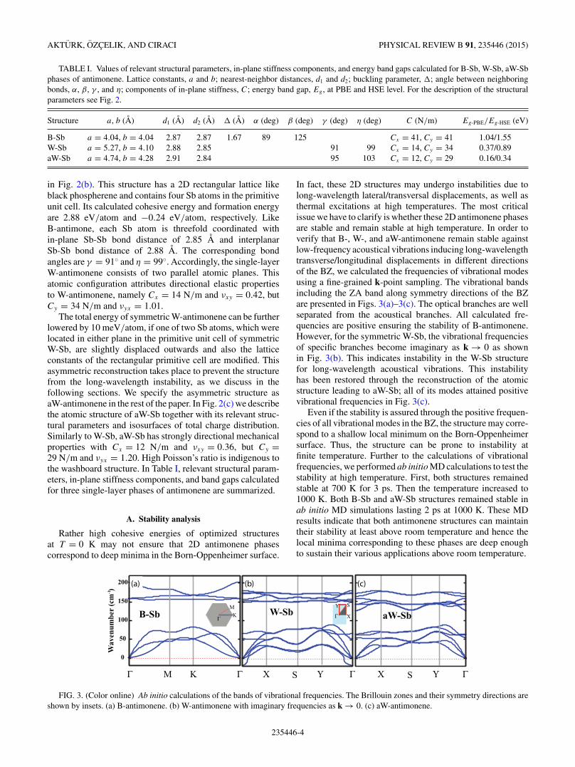
In fact, these 2D structures may undergo instabilities due tolong-wavelength lateral/transversal displacements, as well asthermal excitations at high temperatures. The most criticalissue we have to clarify is whether these 2D antimonene phasesare stable and remain stable at high temperature. In order toverify that B-, W-, and aW-antimonene remain stable againstlow-frequency acoustical vibrations inducing long-wavelengthtransverse/longitudinal displacements in different directionsof the BZ, we calculated the frequencies of vibrational modesusing a fine-grained k-point sampling. The vibrational bandsincluding the ZA band along symmetry directions of the BZare presented in Figs. 3(a)–3(c). The optical branches are wellseparated from the acoustical branches. All calculated fre-quencies are positive ensuring the stability of B-antimonene.However, for the symmetric W-Sb, the vibrational frequenciesof specific branches become imaginary as k → 0 as shownin Fig. 3(b). This indicates instability in the W-Sb structurefor long-wavelength acoustical vibrations. This instabilityhas been restored through the reconstruction of the atomicstructure leading to aW-Sb; all of its modes attained positivevibrational frequencies in Fig. 3(c).
Even if the stability is assured through the positive frequen-cies of all vibrational modes in the BZ, the structure may corre-spond to a shallow local minimum on the Born-Oppenheimersurface. Thus, the structure can be prone to instability atfinite temperature. Further to the calculations of vibrationalfrequencies, we performed ab initio MD calculations to test thestability at high temperature. First, both structures remainedstable at 700 K for 3 ps. Then the temperature increased to1000 K. Both B-Sb and aW-Sb structures remained stable inab initio MD simulations lasting 2 ps at 1000 K. These MDresults indicate that both antimonene structures can maintaintheir stability at least above room temperature and hence thelocal minima corresponding to these phases are deep enoughto sustain their various applications above room temperature.
mc( rebmuneva
W-1)
Γ Μ Κ Γ
Γ
ΜΚ W-Sb aW-Sb
Γ
Γ Χ
SY
B-Sb
Χ S Υ ΓΧ S Υ
0
50
100
150
200 (b) (c)(a)
FIG. 3. (Color online) Ab initio calculations of the bands of vibrational frequencies. The Brillouin zones and their symmetry directions areshown by insets. (a) B-antimonene. (b) W-antimonene with imaginary frequencies as k → 0. (c) aW-antimonene.
235446-4
SINGLE-LAYER CRYSTALLINE PHASES OF ANTIMONY: . . . PHYSICAL REVIEW B 91, 235446 (2015)
Next we address the question of whether the stability ofantimonene phases is affected by vacancy defects. The isolatedvacancy defects are treated by periodically repeating them ina 5 × 5 supercell of antimonene, whereby the coupling withnearest defects is minimized. For a single-vacancy defect inB-Sb, three twofold coordinated Sb atoms around the vacancyare relaxed and form an equilateral triangle, whereby thesecond-nearest-neighbor distance is reduced from 4.05 Ato 3.72 A. Accordingly, the structure around the vacancyis squeezed, but remains symmetric without rebonding ofsurrounding atoms. This situation is in contrast to the vacancyin graphene, where reconstruction or rebonding of carbonatoms surrounding the vacancy is observed [32–34]. Thevacancy formation is an endothermic process and the formationenergy of the single vacancy in B-Sb is 5.03 eV. At the end, thedefect structure remains stable by gaining permanent magneticmoment μ = 1.0 μB per vacancy. The single-vacancy defect inaW-Sb displays similar behavior. Vacancy formation energy isrelatively smaller and is 4.22 eV. Three Sb atoms surroundingthe vacancy undergo a relaxation without rebonding. Theyform a triangle with edges of ∼3.60 A. The single vacancy inthe aW-Sb structure attain also a permanent magnetic momentof 0.6μB per vacancy. Clearly, like B-Sb, the single-vacancydefect does not cause any instability in aW-Sb.
B. Electronic band structure
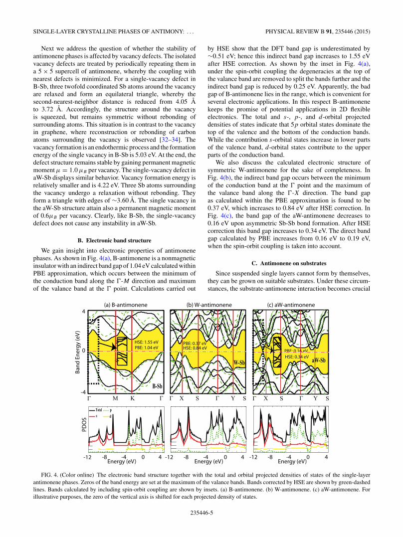
We gain insight into electronic properties of antimonenephases. As shown in Fig. 4(a), B-antimonene is a nonmagneticinsulator with an indirect band gap of 1.04 eV calculated withinPBE approximation, which occurs between the minimum ofthe conduction band along the �-M direction and maximumof the valance band at the � point. Calculations carried out
by HSE show that the DFT band gap is underestimated by∼0.51 eV; hence this indirect band gap increases to 1.55 eVafter HSE correction. As shown by the inset in Fig. 4(a),under the spin-orbit coupling the degeneracies at the top ofthe valance band are removed to split the bands further and theindirect band gap is reduced by 0.25 eV. Apparently, the badgap of B-antimonene lies in the range, which is convenient forseveral electronic applications. In this respect B-antimonenekeeps the promise of potential applications in 2D flexibleelectronics. The total and s-, p-, and d-orbital projecteddensities of states indicate that 5p orbital states dominate thetop of the valence and the bottom of the conduction bands.While the contribution s-orbital states increase in lower partsof the valence band, d-orbital states contribute to the upperparts of the conduction band.
We also discuss the calculated electronic structure ofsymmetric W-antimonene for the sake of completeness. InFig. 4(b), the indirect band gap occurs between the minimumof the conduction band at the � point and the maximum ofthe valance band along the �-X direction. The band gapas calculated within the PBE approximation is found to be0.37 eV, which increases to 0.84 eV after HSE correction. InFig. 4(c), the band gap of the aW-antimonene decreases to0.16 eV upon asymmetric Sb-Sb bond formation. After HSEcorrection this band gap increases to 0.34 eV. The direct bandgap calculated by PBE increases from 0.16 eV to 0.19 eV,when the spin-orbit coupling is taken into account.
C. Antimonene on substrates
Since suspended single layers cannot form by themselves,they can be grown on suitable substrates. Under these circum-stances, the substrate-antimonene interaction becomes crucial
Γ Χ S Γ Y S
PBE: 0.16 eVHSE: 0.34 eV aW-Sb
PBE: 0.37 eVHSE: 0.84 eV
W-Sb
-4
0
4
ΜΓ Κ
B-Sb
ps
Ban
d En
ergy
(eV
)PD
OS
-12 -8 -4 0
Totald
Γ
PBE: 1.04 eVHSE: 1.55 eV
4
-2
2
Γ Χ S Γ Y S
-12 -8 -4 0 4 -12 -8 -4 0 4
(a) B-antimonene (b) W-antimonene (c) aW-antimonene
Energy (eV) Energy (eV) Energy (eV)
-2
2
FIG. 4. (Color online) The electronic band structure together with the total and orbital projected densities of states of the single-layerantimonene phases. Zeros of the band energy are set at the maximum of the valance bands. Bands corrected by HSE are shown by green-dashedlines. Bands calculated by including spin-orbit coupling are shown by insets. (a) B-antimonene. (b) W-antimonene. (c) aW-antimonene. Forillustrative purposes, the zero of the vertical axis is shifted for each projected density of states.
235446-5

AKTURK, OZCELIK, AND CIRACI PHYSICAL REVIEW B 91, 235446 (2015)
0 5 10 150
0.5
1
Distance (Å)
Ener
gy (e
V)
Distance (Å)
-4
0
4
Band
Ene
rgy
(eV
)
Γ M ΓK
3.01Å
2.37Å
0
0.5
1
0 5 10 15
Γ M ΓK-4
0
4
-15 -10 -5 5
Energy (eV) Energy (eV)
Den
sity
of S
tate
s
total
(a)
(b)
(c)
(d)
(e)
(f )
SbGe
free standing antimonene
-2 -1 1 2 2 1 1-2-0 0
-15 -10 -5 0 5{0 {
FIG. 5. (Color online) (a) The optimized atomic structure and binding interaction of B-antimonene grown on germanene surface (i.e.,graphene-like structure of Ge atoms). The registry of Sb and Ge atoms are shown by inset. (b) Corresponding electronic energy band structure.(c) Total and partial densities of states (DOS) projected on Sb and Ge atoms. The comparison of the total density of states of free B-Sbsingle-layer structure with the density of states projected on the Sb atoms grown on germanene indicates significant substrate influence.(d)–(f) Same for B-antimonene grown on the Ge(111) substrate. The zero of energy is set to the Fermi level shown by dash-dotted line.
and may affect the properties revealed for the suspendedsingle layers. To explore to what extent the properties ofgrown layers are influenced we investigated the bindingenergy and electronic band structure of B-Sb grown ongermanene and Ge(111) substrates, which are nearly latticematched.
The atomic structure of B-Sb grown on germanene with AAand AB stacking has been optimized. As shown in Fig. 5(a),we found that AB stacking is favorable energetically and has abinding energy of 250 meV per Sb atom. The equilibriumseparation between Sb and Ge layers is z = 3.01 A. Thismaterial consisting of two single-layer honeycomb structures
is a metal due to a significant interlayer coupling as shownin Fig. 5(b). The comparison made between total DOS offree B-Sb and DOS projected to B-Sb grown on germanenein Fig. 5(c) clearly indicates the influence of germanenesubstrate. The stability and significant interaction betweengermanene and antimonene suggests that composite materialsderived from lateral stacking of (B-Sb)p/(germanene)q (pand q denote the numbers of layers) or their periodicalternation can be fabricated to achieve diverse functionalities.Notably, owing to significant interlayer chemical interactionthis composite structure is rather different from van der Waalsheterostructures.
235446-6
SINGLE-LAYER CRYSTALLINE PHASES OF ANTIMONY: . . . PHYSICAL REVIEW B 91, 235446 (2015)
As an alternative substrate, the Ge(111) surface is consid-ered, which is mimicked by a slab of bulk Ge consisting of three(111) atomic planes. The top and side views of the optimizedatomic structure of B-Sb on the Ge(111) substrate are shownby insets in Fig. 5(d), where the optimized total energy versusthe spacing between Ge(111) and B-Sb is also presented. Thebinding energy is 400 meV per Sb atom, and the equilibriumseparation is 2.37 A. The energy bands corresponding to theequilibrium structure of B-antimonene grown on Ge(111) ismetallic in Fig. 5(e). The total and projected densities ofstates and their comparison with the total density of statesof the free B-Sb single layer in Fig. 5(f) clearly indicatessignificant substrate effects on the properties of antimonene.In particular, the high density of states of the grown Sblayer at the Fermi level is noted. While Ge and germaneneengaged in significant interaction with the grown B-Sb andthey modified its electronic band structure, there might be sub-strates, which do not affect the properties of grown antimonenephases.
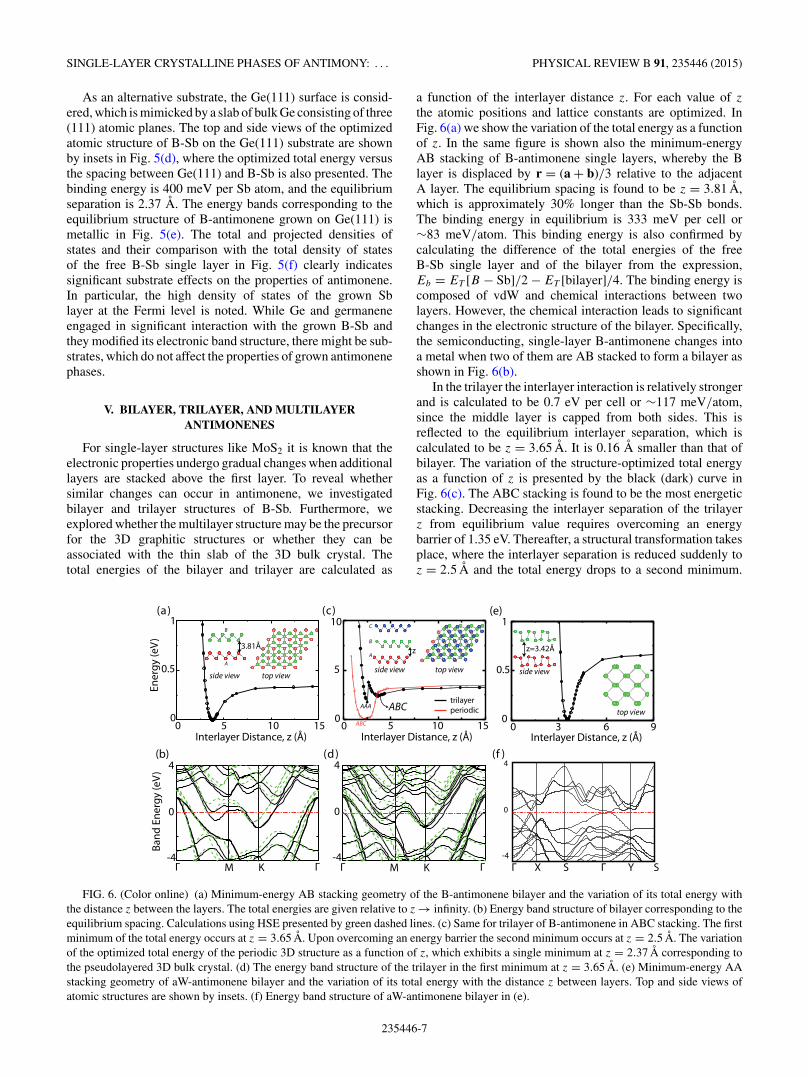
V. BILAYER, TRILAYER, AND MULTILAYERANTIMONENES
For single-layer structures like MoS2 it is known that theelectronic properties undergo gradual changes when additionallayers are stacked above the first layer. To reveal whethersimilar changes can occur in antimonene, we investigatedbilayer and trilayer structures of B-Sb. Furthermore, weexplored whether the multilayer structure may be the precursorfor the 3D graphitic structures or whether they can beassociated with the thin slab of the 3D bulk crystal. Thetotal energies of the bilayer and trilayer are calculated as
a function of the interlayer distance z. For each value of z
the atomic positions and lattice constants are optimized. InFig. 6(a) we show the variation of the total energy as a functionof z. In the same figure is shown also the minimum-energyAB stacking of B-antimonene single layers, whereby the Blayer is displaced by r = (a + b)/3 relative to the adjacentA layer. The equilibrium spacing is found to be z = 3.81 A,which is approximately 30% longer than the Sb-Sb bonds.The binding energy in equilibrium is 333 meV per cell or∼83 meV/atom. This binding energy is also confirmed bycalculating the difference of the total energies of the freeB-Sb single layer and of the bilayer from the expression,Eb = ET [B − Sb]/2 − ET [bilayer]/4. The binding energy iscomposed of vdW and chemical interactions between twolayers. However, the chemical interaction leads to significantchanges in the electronic structure of the bilayer. Specifically,the semiconducting, single-layer B-antimonene changes intoa metal when two of them are AB stacked to form a bilayer asshown in Fig. 6(b).
In the trilayer the interlayer interaction is relatively strongerand is calculated to be 0.7 eV per cell or ∼117 meV/atom,since the middle layer is capped from both sides. This isreflected to the equilibrium interlayer separation, which iscalculated to be z = 3.65 A. It is 0.16 A smaller than that ofbilayer. The variation of the structure-optimized total energyas a function of z is presented by the black (dark) curve inFig. 6(c). The ABC stacking is found to be the most energeticstacking. Decreasing the interlayer separation of the trilayerz from equilibrium value requires overcoming an energybarrier of 1.35 eV. Thereafter, a structural transformation takesplace, where the interlayer separation is reduced suddenly toz = 2.5 A and the total energy drops to a second minimum.
0 5 10 150
0.5
1
Interlayer Distance, z (Å)
Ener
gy (e
V)
Interlayer Distance, z (Å)
Γ M ΓK-4
0
4
-4
0
4
Γ M ΓK
Band
Ene
rgy
(eV
)
3.81Å
A
B
A
B
C
ABC
)c()a(
(b)
(e)
trilayerperiodic
0 3 6 90
0.5
1
Interlayer Distance, z (Å)
-4
0
4
Γ X S Γ Y S
z=3.42Å
top view
side view
)f()d(
1510500
5
10
z
AAA
ABC
top viewside viewtop viewside view
FIG. 6. (Color online) (a) Minimum-energy AB stacking geometry of the B-antimonene bilayer and the variation of its total energy withthe distance z between the layers. The total energies are given relative to z → infinity. (b) Energy band structure of bilayer corresponding to theequilibrium spacing. Calculations using HSE presented by green dashed lines. (c) Same for trilayer of B-antimonene in ABC stacking. The firstminimum of the total energy occurs at z = 3.65 A. Upon overcoming an energy barrier the second minimum occurs at z = 2.5 A. The variationof the optimized total energy of the periodic 3D structure as a function of z, which exhibits a single minimum at z = 2.37 A corresponding tothe pseudolayered 3D bulk crystal. (d) The energy band structure of the trilayer in the first minimum at z = 3.65 A. (e) Minimum-energy AAstacking geometry of aW-antimonene bilayer and the variation of its total energy with the distance z between layers. Top and side views ofatomic structures are shown by insets. (f) Energy band structure of aW-antimonene bilayer in (e).
235446-7

AKTURK, OZCELIK, AND CIRACI PHYSICAL REVIEW B 91, 235446 (2015)
In this transformation, the ABC stacking changes to eitherAAA or ABA stacking. The energy difference between thesetwo different stacking geometries is minute, their bindingenergies approximately 113 meV/atom stronger than thatin the first minimum. Similar structural transformation isexplored for multilayers, which are treated by a periodicallyrepeating structure with . . . ABCABC . . . stacking as inthe 3D pseudolayered bulk crystal in Sec. III. Here thestructure-optimized total energy is calculated as a function ofthe interlayer spacing, z ranging from z = 15 A to z = 2 A.As shown with the red curve in Fig. 6(c), this periodicstructure has a single minimum at z = 2.37 A with thebinding energy of 3.40 eV per cell; it is identical to the3D pseudolayered structure. Accordingly, the single-layerB-antimonene does not construct a 3D graphitic structure withwide interlayer spacing; it rather replicates 3D pseudolayeredbulk crystal as the number of antimonene layers increases.The electronic structure of the trilayer with z = 3.65 A issimilar to that of bilayer and displays a metallic character inFig. 6(d).
In the bilayer of aW-antimonene, the AA stacking attainsthe minimum energy. The equilibrium interlayer separationoccurs at z = 3.42 A and the binding energy is 83 meV asshown in Fig. 6(e). Similar to the bilayer of B-antimonene,the electronic structure exhibits a metallic character withbands crossing at the Fermi level along the �-Y direction inFig. 6(f).
Very recently, Zhang et al. [35] reported results of similarcalculations on B-antimonene, and its bilayer and trilayer.They found the single layer B-Sb as semiconductor. Theirprediction for the fundamental band gap is 2.28 eV with HSEcorrection. Also their energy bands for bilayer and trilayer havezero band gap. The present work, which has been carried outindependently from the work by Zhang et al. [35], has a widerscope comprising not only B-Sb but also 3D bulk, W-Sb, andaW-Sb, and the nanoribbons of diverse edge geometries. Ad-ditionally, our study presents an extensive analysis of stabilityincluding finite-temperature ab initio MD calculations and ex-amines the interaction of B-antimonene grown on germaneneand the Ge(111) surface, and treats antimonene nanoribbonsas presented in forthcoming sections. In the present studythe fundamental band gap was found to be 1.55 eV withthe HSE correction and 0.69 eV with PBE + spin-orbitcoupling.
VI. ELECTRONIC STRUCTURE OF ANTIMONENENANORIBBONS
Since finite-size ribbons or patches of antimonene willbe used in various applications, their stability and electronicproperties become relevant for the characterization of an-timonene phases. Here we consider armchair and zigzagedge geometries, which are specified by the number of Sbatoms, n, in their primitive unit cell. In Fig. 7(a) we showthe primitive unit cell and optimized atomic structure ofthe B-antimonene armchair nanoribbon with n = 22 and thecorresponding electronic energy band structure. Relaxationsoccur mainly at the edges. The B-antimonene nanoribbon hasa nonmagnetic ground state. Two bands, each located at theedge of valence and conduction bands (V and C, respectively)
-2
0
2
Ban
d E
nerg
y (e
V)
0
0.5
1
1.5
Ban
d ga
p (e
V)
10 14 18 22 26 30n
n=22
Relax
d
Γ X
AR
MC
HA
IR
PBE: 0.22 eVHSE: 0.57 eV
20 24 28 32 36 400
0.050.10.150.20.25
Ban
d ga
p (e
V)
2n
-1
-2
0
2
1
Ban
d E
nerg
y (e
V)
2n=32
2x1Z
IGZ
AG
Γ X
(a)
(b) updownHSE up
1
-1
HSE down
HSE: 0.87 eVPBE: 0.20 eV
PBE
HSE
C
V
CV
FIG. 7. (Color online) (a) The primitive unit cell, optimizedatomic configuration, and energy band structure of the armchairB-antimonene nanoribbon. The variation of band gap with n andcharge density isosurfaces of specific band states at the edges ofconduction (C) and valence (V) bands are also shown. Energy bandscorrected using HSE are shown by dashed lines. (b) Same for thezigzag B-antimonene nanoribbon. Structure optimization and bandcalculations are performed using 2 × 1 unit cell. The zero of energyis set at the top of the valence band. Spin-up and spin-down bandsare shown by red and blue lines, respectively. Spin-up and spin-downbands corrected using HSE are also shown by dashed red and bluelines, respectively.
delineate the band gap in the momentum space. They arederived from the states localized at the edges as demonstratedby band-decomposed charge density isosurfaces. The PBEindirect band gap is calculated to be Eg = 0.218 eV, whichincreases to Eg = 0.574 eV after the HSE correction. Thevariation of the PBE band gap Eg with the width of the ribbonor n is also shown.
Since the edge atoms of the zigzag B-Sb nanoribbonundergo a reconstruction, the structure optimization using
235446-8

SINGLE-LAYER CRYSTALLINE PHASES OF ANTIMONY: . . . PHYSICAL REVIEW B 91, 235446 (2015)
the primitive unit cell with n atoms mandates a fictitious,metallic structure. However, upon a Peierls-type structuraltransformation in the 2 × 1 cell, the metallic state changesto ferromagnetic semiconductor. Because of reconstructionthe structure optimization and energy band structures areperformed using the 2 × 1 unit cell. The atomic configuration,energy band structure, and charge density isosurfaces ofspecific states of the zigzag B-Sb with 2n = 32 are presentedin Fig. 7(b). The variation of the band gap with 2n is also
-1
0
1B
and
Ene
rgy
(eV
)
Γ X
AR
MC
HA
IR
n=22
ZIG
ZA
G
2n=32
-1
-2
0
2
Ban
d E
nerg
y (e
V)
Γ X
Ban
d ga
p (e
V)
n
PBE: 0.200 eVHSE: 0.371 eV
12 16 20 24 28
0.1
0.2
0.3
0.4
1
12 16 20 24 28 32 36 40 44 480
0.2
0.4
0.6
0.81
Ban
d ga
p (e
V)
HM M M M M 20 m
eV20
meV
SM
2n
V
C
(a)
(b)
FIG. 8. (Color online) (a) The primitive unit cell having n Sbatoms, optimized atomic structure, and the energy band structureof the armchair aW-antimonene nanoribbon. The variation of bandgap with n and charge density isosurfaces of specific band states atthe edges of conduction (C) and valence (V) bands are also shown.Energy bands calculated by HSE are shown by dashed lines. The zeroof the energy is set at the top of the valence band. (b) Same for thezigzag aW-antimonene nanoribbon, where due to the reconstructionsof edges calculations are performed using 2 × 1 unit cell. Spin-upand spin-down bands are shown by red and blue lines, respectively.The zero of energy is set at the Fermi level.
given in the same figure. The small energy gap betweenfilled spin-up and empty spin-down bands is calculated withinPBE to be Eg = 0.200 eV. Upon HSE correction this bandincreases to 0.872 eV. Isosurfaces of charge density of specificstates at the band edges demonstrate that they are constructedpredominantly from the orbitals of edge atoms. Hence thesestates are localized at the edges of the nanoribbon. The PBEband gap is ∼0.1 eV for 2n = 20, but increases to 0.23 eV for2n = 40.
In Fig. 8(a) we present the atomic configuration andelectronic band structure of armchair and zigzag nanoribbonsof aW-antimonene. The armchair nanoribbon with n = 22is a nonmagnetic semiconductor with a PBE band gap of0.20 eV, which increases to 0.37 eV after HSE correction.Isosurfaces of the selected states at the band edges illustrate thecontribution of the edge atoms. The PBE bands vary between0.1 eV and 0.33 eV depending on the values of n. The zigzagnanoribbon of aW-Sb is treated in a 2 × 1 unit cell due toedge reconstruction. For 2n = 32 the zigzag nanoribbon is ametal. However, the character of the ribbon appears to stronglydepend on its width. Depending on the values of 2n, the zigzagnanoribbon of aW-Sb can exhibit diverse properties, such asmetallic, semimetallic, half-metallic, and semiconducting, asshown in in Fig. 8(b).
VII. CONCLUSIONS
In conclusion, our theoretical study predicts that antimonyatoms can form 2D single-layer crystal structures. One ofthese is named B-antimonene (similar to silicene). The single-layer, symmetric washboard structure (similar to the blackphosphorene) is, however, unstable against long-wavelengthdisplacements. If the lattice constants of rectangular structurechange and one of two Sb atoms on the top and bottomatomic planes of symmetric washboard structure are buckled,the total energy can be further lowered. The resulting newstructure is called aW-antimonene. That these 2D single-layerB- and aW-antimonene structures are stable was concludednot only based on the structure optimizations achieved by theconjugate gradient method but also based on other tests, suchas ab initio calculation of vibration frequencies and ab initiomolecular dynamics calculations performed at temperaturesas high as 1000 K. We showed also that antimonene phasesare robust against vacancy formation. B-antimonene andaW-antimonene are semiconductors with band gaps suitablefor their use in 2D electronics. These single-layer phasesof antimony can form stable bilayers, trilayers, and evenmultilayers. Because of significant interlayer coupling, bilayerand multilayer structures are metallic. We examined theeffect of substrates for B-antimonene grown on germaneneand the Ge(111) surface. We found a significant influenceof these substrates on the grown B-antimonene, wherebythe semiconducting single layer of antimonene changesinto metal. Nanoribbons of antimonene phases display adiversity of properties depending on their width and edgegeometry. Usually they are narrow band gap semiconductorsand attain magnetic properties for zigzag edge geometry.Accordingly, the band gap can be engineered by varyingthe width of these nanoribbons. The stability and significantbinding energy suggest the fabrication of composite materials
235446-9

AKTURK, OZCELIK, AND CIRACI PHYSICAL REVIEW B 91, 235446 (2015)
consisting of vertically stacked antimonene and germaneneheterostructures. Briefly, our study heralds stable structuresderived from antimonene, such as multilayers and composites,2D single layers, bilayers, trilayers, and 1D nanoribbons.They display diverse properties for various technologicalapplications.
ACKNOWLEDGMENTS
The computational resources are provided by TUBITAKULAKBIM, High Performance and Grid Computing Center(TR-Grid e-Infrastructure). V.O.O. and S.C. acknowledgefinancial support from the Academy of Sciences of Turkey(TUBA).
[1] E. Durgun, S. Tongay, and S. Ciraci, Phys. Rev. B 72, 075420(2005).
[2] S. Cahangirov, M. Topsakal, E. Akturk, H. Sahin, and S. Ciraci,Phys. Rev. Lett. 102, 236804 (2009).
[3] P. Vogt, P. DePadova, C. Quaresima, J. Avila, E. Frantzeskakis,M. C. Asensio, A. Resta, B. Ealet, and G. LeLay, Phys. Rev.Lett. 108, 155501 (2012).
[4] V. O. Ozcelik, E. Durgun, and S. Ciraci, J. Phys. Chem. Lett. 5,2694 (2014).
[5] Y. Xu, B. Yan, H. J. Zhang, J. Wang, G. Xu, P. Tang, W. Duan,and S. C. Zhang, Phys. Rev. Lett. 111, 136804 (2013).
[6] H. Sahin, S. Cahangirov, M. Topsakal, E. Bekaroglu, E. Akturk,R. T. Senger, and S. Ciraci, Phys. Rev. B 80, 155453 (2009).
[7] S. Tongay, S. Dag, E. Durgun, R. T. Senger, and S. Ciraci, J.Phys.: Condens. Matter 17, 3823 (2005).
[8] D. Malko, C. Neiss, F. Vines, and A. Gorling, Phys. Rev. Lett.108, 086804 (2012).
[9] V. O. Ozcelik and S. Ciraci, J. Phys. Chem. C 117, 2175 (2013).[10] V. O. Ozcelik, S. Cahangirov, and S. Ciraci, Phys. Rev. Lett.
112, 246803 (2014).[11] X. Xu, J. Zhuang, Y. Du, H. Feng, N. Zhang, C. Liu, T. Lei,
J. Wang, M. Spencer, T. Morishita, X. Wang, and S. X. Dou,Sci. Rep. 4, 7543 (2014).
[12] P. Joensen, R. F. Frindt, and S. R. Morrison, Mater. Res. Bull.21, 457 (1986).
[13] J. N. Coleman, M. Lotya, A. O’Neill, S. D. Bergin, P. J. King,U. Khan, and K. Young, Science 331, 568 (2011).
[14] C. Ataca and S. Ciraci, J. Phys. Chem. C 115, 13303 (2011).[15] C. Ataca, H. Sahin, and S. Ciraci, J. Phys. Chem. C 116, 8983
(2012).[16] L. Li, Y. Yu, G. J. Ye, Q. Ge, X. Ou, H. Wu, D. Feng, X. H.
Chen, and Y. Zhang, Nat. Nanotechnol. 9, 372 (2014).
[17] Z. Zhu and D. Tomanek, Phys. Rev. Lett. 112, 176802 (2014).[18] T. Low, A. S. Rodin, A. Carvalho, Y. Jiang, H. Wang, F. Xia,
and A. H. Castro Neto, Phys. Rev. B 90, 075434 (2014).[19] C. Maanit, A. McKinley, and R. H. Williams, J. Phys. C: Solid
State Phys. 18, 4975 (1985).[20] M. W. Grant, P. F. Lyman, J. H. Hoogenraad, and L. E.
Seiberling, Surf. Sci. 279, L180 (1992).[21] R. Whittle, I. T. McGovern, D. R. T. Zahn, C. Muller, C. Nowak,
A. Cafolla, and W. Braun, Appl. Surf. Sci. 56, 218 (1992).[22] S. Grimme, J. Comput. Chem. 27, 1787 (2006).[23] C. Ataca, M. Topsakal, E. Akturk, and S. Ciraci, J. Phys. Chem.
C 115, 16354 (2011).[24] P. E. Blochl, Phys. Rev. B 50, 17953 (1994).[25] J. P. Perdew, K. Burke, and M. Ernzerhof, Phys. Rev. Lett. 77,
3865 (1996).[26] G. Kresse and J. Furthmuller, Phys. Rev. B 54, 11169 (1996).[27] H. J. Monkhorst and J. D. Pack, Phys. Rev. B 13, 5188 (1976).[28] J. Paier, M. Marsman, K. Hummer, G. Kresse, I. C. Gerber, and
J. G. Angyan, J. Chem. Phys. 124, 154709 (2006).[29] D. Alfe, Comput. Phys. Commun. 180, 2622 (2009).[30] C. Kittel, Introduction to Solid State Physics, 8th ed. (John Wiley
& Sons, New York, 1996).[31] C. S. Barrett, P. Cucka, and K. Haefner, Acta Cryst. 16, 451
(1963).[32] O. V. Yazyev and L. Helm, Phys. Rev. B 75, 125408 (2007).[33] A. W. Robertson, B. Montanari, K. He, C. S. Allen, Y. A. Wu,
N. M. Harrison, A. I. Kirkland, and J. H. Warner, ACS Nano 7,4495 (2013).
[34] V. O. Ozcelik, H. H. Gurel, and S. Ciraci, Phys. Rev. B 88,045440 (2013).
[35] Z. Zhang, Z. Yan, Y. Li, Z. Chen, and H. Zeng, Angew. Chem.Int. Ed. 54, 3112 (2015).
235446-10