SINGLE EVENT EFFECTS TEST REPORT RADEF/JYFL, FINLAND HIF/UCL ... - TI.com · ADS5463MHFG-V Part...
22
HIREX Engineering SAS au capital de 180 000 € - RCS Toulouse B 389 715 525 Siège social: 2 rue des Satellites - 31520 Toulouse SINGLE EVENT EFFECTS TEST REPORT Test Type: Heavy Ion Test facility: RADEF/JYFL, FINLAND HIF/UCL, BELGIUM Test Date: June 2012 Part Types: ADS5463MHFG-V Part Description: 12-Bit, 500-MSPS Analog-to-Digital Converter Part Manufacturer: Texas Instruments Texas Instruments Purchase Order No 4512326671 dated 15/03/2012 item 020 Hirex reference : HRX/SEE/0416 Issue : 01 Date : June 26, 2012 Written by : M. Mazurek Design Engineer Authorized by: F.X. Guerre Study Manager
Transcript of SINGLE EVENT EFFECTS TEST REPORT RADEF/JYFL, FINLAND HIF/UCL ... - TI.com · ADS5463MHFG-V Part...
HIREX Engineering SAS au capital de 180 000 € - RCS Toulouse B 389 715 525 Siège social: 2 rue des Satellites - 31520 Toulouse
SINGLE EVENT EFFECTS TEST REPORT
Test Type: Heavy Ion
Test facility: RADEF/JYFL, FINLAND HIF/UCL, BELGIUM
Test Date: June 2012
Part Types: ADS5463MHFG-V
Part Description: 12-Bit, 500-MSPS Analog-to-Digital Converter
Part Manufacturer: Texas Instruments
Texas Instruments Purchase Order No 4512326671 date d 15/03/2012 item 020 Hirex reference : HRX/SEE/0416 Issue : 01 Date : June 26, 2012
Written by : M. Mazurek Design Engineer
Authorized by: F.X. Guerre Study Manager

Hirex Engineering SEE Test Report Ref. : HRX/SEE/0416
Issue : 01
HRX/SEE/0416 Issue 01 Page 2 / 22
RESULTS SUMMARY
Facility RADEF/JYFL, Finland HIF/UCL, Belgium Test date June 2012 Device description
Part type: ADS5463MHFG-V Description: 12-Bit, 500-MSPS Analog-to-Digital Converter Package: CQFP 84 Die dimensions: 5123 µm x 5135µm
SEL Results
No SEL was observed up to LET of 86 MeV/(mg/cm2) at 85°C and 125°C temperatures, a bias voltage AVDD = +5.25V, DV DD = +3.6V, AV DD = +3.6V and a fluence of 1.0E+07 ions/cm² for tw o samples.
SET on the reference voltage 140 SETs on the reference voltage signal were obser ved. They started to appear from Nitrogen ion (LET of 1.8 MeV/(mg/cm2) .
SEU Cross-Section The SEU cross-section reaches its highest value at 1.8E-04 cm2/device while the LET threshold below 1.8 MeV/(mg/cm²).
SEU Results Details o 555 events have been detected over the whole LET r ange from 1.87 to 85.9 MeV/(mg/cm 2)
SEU events were classified in three main categories depending on the SEU duration: • SEU ‘A‘– short conversion errors with maximum 10 c onsecutive samples in error • SEU ‘B’ – long conversion errors with more than 10 consecutive samples in error with digital
signature, and for which an SET on Vref signal occu rred at the same time • SEU ‘C’ – long conversion errors with more than 10 consecutive samples in error with analog
signature, and for which an SET on Vref signal occu rred at the same time
1.0E-07
1.0E-06
1.0E-05
1.0E-04
1.0E-03
0 10 20 30 40 50 60 70 80 90 100
SE
U X
-se
ctio
n/D
ev
ice
(cm
²)
Eff LET (MeV/mg/cm²)
ADS5463 Convertre, SEU X-Section/Device
ADS5463 DUT #27
ADS5463 DUT #166
Weibull Fit
ADS5463MHFG-V
AVDD = +4.75V, DVDD = +3.0V, AVDD = +3.0V
S 1
W 50
x0 0.9
A 1.80E-04

Hirex Engineering SEE Test Report Ref. : HRX/SEE/0416
Issue : 01
HRX/SEE/0416 Issue 01 Page 3 / 22
DOCUMENTATION CHANGE NOTICE Issue Date Page Change Item
01
26/06/2012
All
Original issue
Contributors to this work: Maria Mazurek Hirex Engineering Bertrand Forgerit Hirex Engineering F.X. Guerre Hirex Engineering
Hirex Engineering SEE Test Report Ref. : HRX/SEE/0416
Issue : 01
HRX/SEE/0416 Issue 01 Page 4 / 22
SEE TEST REPORT
TABLE OF CONTENTS
1 INTRODUCTION ..................................................................................................................................................... 5
2 APPLICABLE AND REFERENCE DOCUMENTS ............................................................................................. 5
2.1 APPLICABLE DOCUMENTS .................................................................................................................................... 5 2.2 REFERENCE DOCUMENTS ..................................................................................................................................... 5
3 DEVICE INFORMATION ....................................................................................................................................... 6
3.1 DEVICE DESCRIPTION ........................................................................................................................................... 6 3.2 SAMPLE IDENTIFICATION ...................................................................................................................................... 6 3.3 STACK CONSTRUCTION ANALYSIS ....................................................................................................................... 7 3.4 EFFECTIVE LET CALCULATION ............................................................................................................................ 9
4 TEST SET-UP ......................................................................................................................................................... 10
4.1 TEST SYSTEM ..................................................................................................................................................... 10 4.2 ADC TEST PRINCIPLE ......................................................................................................................................... 10
5 RADEF TEST FACILITY ..................................................................................................................................... 13
6 HIF TEST FACILITY ............................................................................................................................................ 14
7 SEE TEST RESULTS ............................................................................................................................................. 15
7.1 SEL.................................................................................................................................................................... 15 7.2 SET ON THE REFERENCE VOLTAGE .................................................................................................................... 16 7.3 SEU ................................................................................................................................................................... 16
8 GLOSSARY ............................................................................................................................................................. 20
9 DETAILED RESULTS PER RUN ........................................................................................................................ 21
9.1 DETAILED RUN TABLE ........................................................................................................................................ 22
LIST OF FIGURES Figure 1: Device identification for the ADS5463MHFG -V part ..................................................................... 6 Figure 2: Material identification and thickness mea sures for the ADS5463MHFG-V part ........................ 7 Figure 3: Die microsection for the ADS5463MHFG-V pa rt ........................................................................... 8 Figure 4: Effective LET definition for min and max cases ........................................................................... 9 Figure 5: Effective LET values at active DUT area c omputed with SRIM2006 ........................................... 9 Figure 6: Heavy Ion test set-up ..................................................................................................................... 10 Figure 7: The DAC-ADC test chain ............................................................................................................... 10 Figure 8: Example of initial calibration results ........................................................................................... 11 Figure 9: Test conditions for the ADS5463MHFG-V par t ........................................................................... 12 Figure 10: DUT bias description ................................................................................................................... 12 Figure 11: SEU X-section/device for the ADS5463MHFG -V part; JYFL, UCL June 2012 ........................ 15 Figure 12: Weibull parameters for the ADS5463MHFG- V part; JYFL, UCL June 2012 ........................... 15 Figure 13: Typical SEU events; JYFL, UCL June 2012 ................................................................................... 16 Figure 14: Typical SEU events for each category; JY FL, UCL June 2012 ................................................ 17 Figure 15: Events types for each used ion (all con ditions and all DUTs together); JYFL, UCL June
2012 .......................................................................................................................................................... 17 Figure 16: Definition of SEU Amplitude and SEU Dura tion ....................................................................... 18 Figure 17: Amplitude versus duration at all used io ns; JYFL, UCL June 2012 ....................................... 19
LIST OF TABLES Table 1: RADEF, Used ion and features thereof; JYFL June 2012 ............................................................ 14 Table 2: HIF, Used ion and features thereof; UCL Ju ne 2012 ......................................................................... 14 Table 3: Run Table for the ADS5463MHFG-V part; JYFL , UCL June 2012 ............................................... 22

Hirex Engineering SEE Test Report Ref. : HRX/SEE/0416
Issue : 01
HRX/SEE/0416 Issue 01 Page 5 / 22
1 Introduction This report presents the results of Heavy Ion test program carried out on Texas Instruments 12-Bit, 500-MSPS Analog-to-Digital Converter referenced ADS5463MHFG-V. Two devices were heavy ion tested at RADEF, Univers ity of Jyväskylä, Department of Physics, Jyväskylä, Finland in June 2012. Additional tests with Xenon ion were performed at H IF, UCL University of Louvain, Belgium. This work was performed for Texas Instruments Purch ase Order No 4512326671 dated 15/03/2012 item 020
2 Applicable and Reference Documents
2.1 Applicable Documents AD-1. 12-Bit, 500-MSPS Analog-to-Digital Converters datasheet ; Revised July 2009 AD-2. Hirex proposal HRX/PRO/3809 Issue 02, dated M arch 12, 2012
2.2 Reference Documents RD-1. Single Event Effects Test method and Guidelin es ESA/SCC basic specification No 25100

Hirex Engineering SEE Test Report Ref. : HRX/SEE/0416
Issue : 01
HRX/SEE/0416 Issue 01 Page 6 / 22
3 DEVICE INFORMATION
3.1 Device description The ADS5463MHFG-V is a 12-bit 500-MSPS analog-to-di gital converter (ADC) that operates from 5V supply and 3.3V supply, while providing LVDS-compat ible digital outputs from a 3.3V supply. Part Type: ADS5463MHFG-V Manufacturer: Texas Instruments Package: CQFP 84 Samples Used: #027, #166 Top Marking: 5962 – 0720801VXC ADS5463MHFG-V THA 8AAR 1121A Q Die dimensions: 5123 µm x 5135µm
3.2 Sample identification Texas Instruments has delivered four ADS5463MHFG-V samples with the lot datecode of “1121A”. Three of them were prepared to be tested to heavy i ons. The fourth part was used for a die microsection. A die size is small comparing to the device cavity, so package shadowing is not an obstacle. The test was performed on two samples.
Photo 1 - Top Marking (ADS5463MHFG-V) Photo 2 - Die Marking ( ADS5463MHFG-V)
Photo 3 – Full view (ADS5463MHFG-V)
Figure 1: Device identification for the ADS5463MHFG -V part

Hirex Engineering SEE Test Report Ref. : HRX/SEE/0416
Issue : 01
HRX/SEE/0416 Issue 01 Page 7 / 22
3.3 Stack Construction Analysis Die microsections were performed on the ADS5463MHFG -V part in order to check ion penetration. Dead layer was measured and will be taken into acco unt for computing the effective LET value.
Layer ID Material Thickness
Passivation Si3N4/ SiO2 /SiO2 1µm/ 0.3µm/ 0.5µm
Metal 4 Al Cu, TiW liner 1.5µm /0.18µm
Via plug W 0.6µm diam.
Inter Layer Dielectric 4 SiO2 / SOG / SiO2 cap 0.8µm / 0 to 0.8µm / ~60nm
Metal 3 TiW ARC , Al (Cu), TiW liner 50nm/0.57µm/ 150nm
Via plug W 0.6µm diam
Inter Layer Dielectric 3 SiO2 / SOG / SiO2 cap 0.2µm/0 to 0.2µm/~60nm
Metal 2 TiW ARC , Al (Cu), TiW liner ~50nm/0.57µm/ 200nm
Via plug W 0.6µm diam
Inter Layer Dielectric 2 SiO2 / SOG / SiO2 cap 0.2µm/0 to 0.2µm/~60nm
Metal 1 TiW ARC , Al (Cu), TiW liner 50nm/0.57µm/ 150nm
Contact plug W 0.6µm diam
Inter Layer Dielectric 1 SiO2 0.46 to 0.85µm
Nitride liner Si3N4 ~ 50nm
Poly 2 Polysilicon 270nm
Poly 1 Polysilicon Thickness 325nm, Cd’s 950-
500 nm
Gate oxide Under Detection Limit Under Detection Limit
STI SiO2 480nm ( Ox trench 1.6µm)
Epitaxy Silicon 1µm
Burried oxide Thermal oxyde 123nm
Figure 2: Material identification and thickness mea sures for the ADS5463MHFG-V part

Hirex Engineering SEE Test Report Ref. : HRX/SEE/0416
Issue : 01
HRX/SEE/0416 Issue 01 Page 8 / 22
Figure 3: Die microsection for the ADS5463MHFG-V pa rt

Hirex Engineering SEE Test Report Ref. : HRX/SEE/0416
Issue : 01
HRX/SEE/0416 Issue 01 Page 9 / 22
3.4 Effective LET calculation Taking into account passivation, metals, and dielec tric layers, effective LET values at active DUT surface are computed with the use of SRIM2006 1.
Active Area
Passivation Layer
Min Case
Dielectric Layer
Effective LET
LET at DUT surface
Active Area
Passivation Layer
Max Case
Dielectric 4 Layer
Metal 4 Layer
LET at DUT surface
Dielectric 3 Layer
Metal 3 Layer
Dielectric 2 Layer
Metal 2 Layer
Dielectric 1 Layer
Metal 1 Layer
Effective LET
Figure 4: Effective LET definition for min and max cases
Figure 5: Effective LET values at active DUT area c omputed with SRIM2006
1 http://www.srim.org/SRIM/SRIMLEGL.htm
Used ions
Ion energy
Nitrogen
(139 MeV)
Neon
(235MeV)
Argon
(372MeV)
Iron
(523MeV)
Krypton
(756MeV)
Xenon
(420MeV)
LET @ DUT
surface (MeV) 1.8 3.6 10.2 18.5 32.2 69.0
Min Case Eff. LET (MeV) 1.8 3.7 10.4 19.1 33.0 67.7
Max Case Eff. LET (MeV) 1.8 3.9 10.9 20.5 34.9 58.0
Bragg Peak Eff. LET(MeV) 5.9 9.0 19.6 29.3 41.0 69.2
Hirex Engineering SEE Test Report Ref. : HRX/SEE/0416
Issue : 01
HRX/SEE/0416 Issue 01 Page 10 / 22
4 Test Set-up
4.1 Test system
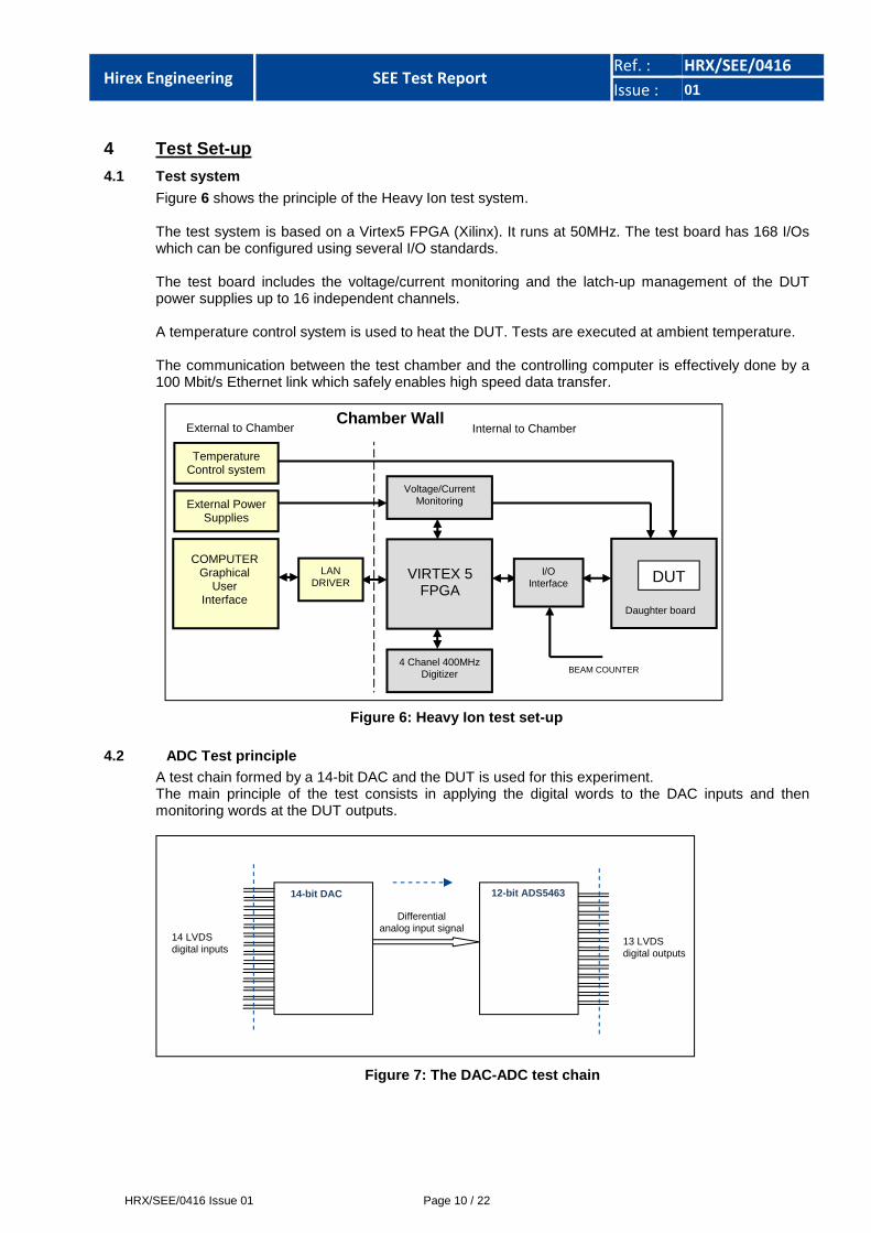
Figure 6 shows the principle of the Heavy Ion test system. The test system is based on a Virtex5 FPGA (Xilinx) . It runs at 50MHz. The test board has 168 I/Os which can be configured using several I/O standards .
The test board includes the voltage/current monitor ing and the latch-up management of the DUT power supplies up to 16 independent channels. A temperature control system is used to heat the DU T. Tests are executed at ambient temperature. The communication between the test chamber and the controlling computer is effectively done by a 100 Mbit/s Ethernet link which safely enables high speed data transfer.
Figure 6: Heavy Ion test set-up
4.2 ADC Test principle A test chain formed by a 14-bit DAC and the DUT is used for this experiment. The main principle of the test consists in applying the digital words to the DAC inputs and then monitoring words at the DUT outputs.
Figure 7: The DAC-ADC test chain
14-bit DAC 12-bit ADS5463
14 LVDS digital inputs
13 LVDS digital outputs
Differential analog input signal
VIRTEX 5 FPGA
COMPUTER Graphical
User Interface
External Power Supplies
LAN DRIVER
Voltage/Current Monitoring
Chamber Wall
I/O Interface
BEAM COUNTER
Internal to Chamber External to Chamber
Temperature Control system
Daughter board
DUT
4 Chanel 400MHz Digitizer

Hirex Engineering SEE Test Report Ref. : HRX/SEE/0416
Issue : 01
HRX/SEE/0416 Issue 01 Page 11 / 22
Test chain calibration
Before starting the experiment a calibration of the DUT in real test conditions is performed (under vacuum and at test temperature). This test chain calibration consists in acquiring f or each input step (16384 steps of the 14-bit DAC), the 13-bit ADC output value. For each input step 2.0E+6 conversions are performe d and min and max ADC output values are recorded. These min and max levels thresholds form an error range for each input word. Figure 9 shows a calibration example used in Run 10. Min va lue, max value and delta (max-min) are plotted for each DAC word. It can be observed that for most of the DAC inputs the delta conversion error is between 12 and 16 ADC LSBs.
0
5
10
15
20
25
0
500
1000
1500
2000
2500
3000
3500
4000
0 2000 4000 6000 8000 10000 12000 14000 16000
De
lta
[LS
B]
Min
/Ma
x [L
SB]
DAC word input
Calibration example (used in RUN 10)
Min
Max
Delta
Figure 8: Example of initial calibration results
SEU
Each run consists in continuously applying 16384 (2 ^14) words at the DAC inputs. Each word is converted 4.0E+6 times at a conversion sampling fre quency of 400MSPS, which corresponds to 10ms. For each input word, the ADC outputs are compared w ith the min and the max values recorded during the calibration stage increased by 12 LSB to prevent from noisy events (Min - 12LSB, Max + 12LSB). If these values are exceeded, a conversion error is detected and counted.
Reference voltage monitoring
The internal reference voltage is measured at VREF pin. The signal is digitized with a 12-bit ADC converter (1LSB~ 0.977 mV) at 40MSPS and 2 threshol ds (low and high) are programmed.
SEL
SEL detection is performed by monitoring the DUT su pply currents. When a SEL occurs (over 1A), then device is switched off during 1 second, and th e SEL event is registered in the log file. The SEL threshold can be adjusted during the test, but in general it is adjusted before starting the test. During all irradiation time, the supply curre nts of each DUT are measured.

Hirex Engineering SEE Test Report Ref. : HRX/SEE/0416
Issue : 01
HRX/SEE/0416 Issue 01 Page 12 / 22
Test conditions
Runs are performed with selected ions: 15N+4, 20Ne+ 6, 40Ar+12, 56Fe+15, 82Kr+22, 124Xe25+ and at two different tilt angles (0 deg. and 38 deg .) The tests are done at three different temperatures: room temperature, 85°C and 125°C. All values of the voltage supplies are presented in Figure 9 ).
Test Test condition number
AVDD DVDD AVDD Tilt angle (°) Temperature (°C)
SEU 1 +4.75V +3.0V +3.0V 0° room
SEU 2 +4.75V +3.0V +3.0V 38° room
SEL 3 +5.25V +3.6V +3.6V 0° 85°C
SEL 4 +5.25V +3.6V +3.6V 38° 85°C
SEL 5 +5.25V +3.6V +3.6V 0° 125°C
SEL 6 +5.25V +3.6V +3.6V 38° 125°C
Figure 9: Test conditions for the ADS5463MHFG-V par t
Figure 10: DUT bias description

Hirex Engineering SEE Test Report Ref. : HRX/SEE/0416
Issue : 01
HRX/SEE/0416 Issue 01 Page 13 / 22
5 RADEF Test Facility Test at the cyclotron accelerator was performed at University of Jyvaskyla (JYFL) (Finland) under HIREX Engineering responsibility. The facility includes a special beam line dedicated to irradiation studies of semiconductor components and devices. It consists of a vacuum cha mber including component movement apparatus and the necessary diagnostic equipment re quired for the beam quality and intensity analysis. The cyclotron is a versatile, sector-focused accele rator of beams from hydrogen to xenon equipped with three external ion sources: two electron cyclo tron resonance (ECR) ion sources designed for high-charge-state heavy ions, and a multicusp ion s ource for intense beams of protons. The ECR's are especially valuable in the study of single even t effects (SEE) in semiconductor devices. For heavy ions, the maximum energy attainable can be determin ed using the formula
130 Q2/M,
where Q is the ion charge state and M is the mass i n Atomic Mass Units. Test chamber Irradiation of components is performed in a vacuum chamber with an inside diameter of 75 cm and a height of 81 cm. The vacuum in the chamber is achieved after 15 minu tes of pumping, and the inflation takes only a few minutes. The position of the components install ed in the linear movement apparatus inside the chamber can be adjusted in the X, Y and Z direction s. The possibility of rotation around the Y-axis is provided by a round table. The free movement area r eserved for the components is 25 cm x 25 cm, which allows one to perform several consecutive irr adiations for several different components without breaking the vacuum. The assembly is equipped with a standard mounting f ixture. The adapters required accommodating the special board configurations and the vacuum fee d-throughs can also be made in the laboratory’s workshops. The chamber has an entrance door, which allows rapid changing of the circuit board or individual components. A CCD camera with a magnifying telescope is located at the other end of the beam line to determine accurate positioning of the components. The coordin ates are stored in the computer’s memory allowing fast positioning of various targets during the test.
Beam quality control For measuring beam uniformity at low intensity, a C sI(Tl) scintillator with a PIN-type photodiode readout is fixed in the mounting fixture. The unifo rmity is measured automatically before component irradiation and the results can be plotted immediat ely for more detailed analysis. A set of four collimated PIN-CsI(Tl) detectors is l ocated in front of the beam entrance. The detectors are operated with step motors and are located at 90 degrees with respect to each other. During the irradiation and uniformity scan they are set to the outer edge of the beam in order to monitor the stability of the homogeneity and flux. Two beam wobblers and/or a 0.5 microns diffusion Go ld foil can be used to achieve good beam homogeneity. The foil is placed 3 m in front of the chamber. The wobbler-coils vibrate the beam horizontally and vertically, the proper sweeping ar ea being attained with the adjustable coil-currents .
Dosimetry The flux and intensity dosimeter system contains a Faraday cup, several collimators, a scintillation counter and four PIN-CsI(Tl) detectors. Three colli mators of different size and shape are placed 25 cm in front of the device under test. They can be u sed to limit the beam to the active area to be studied. At low fluxes a plastic scintillator with a photomu ltiplier tube is used as an absolute particle count er. It is located behind the vacuum chamber and is used be fore the irradiation to normalize the count rates of the four PIN-CsI(Tl) detectors. JYFL facility is an ESA qualified heavy ion facilit y. Compliance for beam uniformity and fluence dosimetry to ESA/SCC 25100 requirements are under J YFL responsibility. For the present test, beam rectangular collimator w as set to 20mm by 40 mm.
Used ions The RADEF ion used is listed in the table below.
Hirex Engineering SEE Test Report Ref. : HRX/SEE/0416
Issue : 01
HRX/SEE/0416 Issue 01 Page 14 / 22
Table 1: RADEF, Used ion and features thereof; JYFL June 2012
6 HIF Test Facility Test at the cyclotron accelerator was performed at “Université Catholique de Louvain” (UCL) (Louvain-La-Neuve, Belgium) under HIREX Engineering responsibility. In collaboration with the European Space Agency (ESA), the needed equipment f or single events studies using heavy ions was built and installed on the HIF beam line in the experimental hall of Louvain-La-Neuve cyclotron. CYCLONE is a multi particle, variable energy, cyclo tron capable of accelerating protons (up to 75 MeV), alpha particles and heavy ions. For the heavy ions, the covered energy range is between 0.6 MeV/AMU and 27.5 MeV/AMU. For these ions, the maxim al energy can be determined by the formula:
110 Q2/M
Where Q is the ion charge state and M is the mass i n Atomic Mass Units.
The heavy ions are produced in a double stage Elect ron Cyclotron Resonance (ECR) source. Such a source allows producing highly charged ions and ion "cocktails". These are composed of ions with the same or very close M/Q ratios. The cocktail ion s are injected in the cyclotron, accelerated at the same time and extracted separately by a fine tuning of the magnetic field or a slight changing of the RF frequency. This method is very convenient for a quick change of ion (in a few minutes) which is equivalent to a LET variation.
Dosimetry The current UCL Cyclotron dosimetry system and proc edures were used.
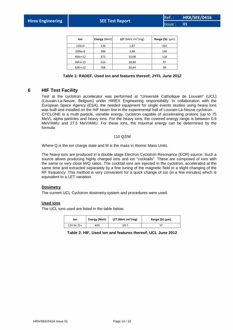
Used ions The UCL ions used are listed in the table below.
Ion Energy (MeV) LET (MeV.cm²/mg) Range (Si) (µm)
124 Xe 25+ 420 69.7 37
Table 2: HIF, Used ion and features thereof; UCL Ju ne 2012
Ion Energy (MeV) LET (MeV.cm²/mg) Range (Si) (µm)
15N+4 139 1,87 202
20Ne+6 186 3,68 146
40Ar+12 372 10,08 118
56Fe+15 523 18,84 97
82Kr+22 768 30,44 94

Hirex Engineering SEE Test Report Ref. : HRX/SEE/0416
Issue : 01
HRX/SEE/0416 Issue 01 Page 15 / 22
7 SEE Test Results Two samples have been exposed over a LET range from 1.87 to 85.9 MeV/(mg/cm²) at ambient temperature for SEU characterization. In addition, tests with Xenon at 38 degrees and two different temperatures (85°C, 125°C) have been performed for SEL identification. Detailed results per run are presented in Table 3 . The corresponding single event cross-section per device is shown in Figure 11 and the Weibull parameters are summarized in Figure 12 . The SEU cross-section reaches its highest value at 1.8E-04 cm2/device while the LET threshold below 1.87 MeV/(mg/cm²).
1.0E-07
1.0E-06
1.0E-05
1.0E-04
1.0E-03
0 10 20 30 40 50 60 70 80 90 100
SE
U X
-se
ctio
n/D
ev
ice
(cm
²)
Eff LET (MeV/mg/cm²)
ADS5463 Convertre, SEU X-Section/Device
ADS5463 DUT #27
ADS5463 DUT #166
Weibull Fit
Figure 11: SEU X-section/device for the ADS5463MHFG -V part; JYFL, UCL June 2012
Figure 12: Weibull parameters for the ADS5463MHFG- V part; JYFL, UCL June 2012
7.1 SEL No SEL was observed up to LET of 86 MeV/(mg/cm2) at 85°C and 125°C temperatures, a bias voltage AVDD = +5.25, DV DD = +3.6V, AV DD = +3.6V and a fluence of 1.0E+07 ions/cm² for two samples.
ADS5463MHFG-V
AVDD = +4.75V, DVDD = +3.0V, AVDD = +3.0V
S 1
W 50
x0 0.9
A 1.8E-04

Hirex Engineering SEE Test Report Ref. : HRX/SEE/0416
Issue : 01
HRX/SEE/0416 Issue 01 Page 16 / 22
7.2 SET on the reference voltage A threshold of +/- 5 mV was used when monitoring th e reference voltage output. SETs smaller than 5mV could not be detected. 140 SETs on the reference voltage signal were obser ved. They started to appear from Nitrogen ion (LET of 1.8 MeV/(mg/cm2) . Figure 13 presents an example of the transient on t he Vref signal and a conversion error caused by this transient.
740
760
780
800
820
840
860
880
2.35
2.4
2.45
2.5
2.55
0 500 1000 1500 2000
SEU
_2
17
Re
fere
nce
vo
lta
ge [
V]
Time [ns]
Typical SET on Vref signal; RUN 48
Figure 13: Typical SEU events; JYFL, UCL June 2012
7.3 SEU Conversion events were detected over the LET range from 1.8 to 85.9 MeV/(mg/cm2) , resulting in a total of 555 events. SEU events were classified in three main categories depending on the SEU duration:
• SEU ‘A‘– short conversion errors with maximum 10 c onsecutive samples in error • SEU ‘B’ – long conversion errors with more than 10 consecutive samples in error with digital
signature, and for which an SET on Vref signal occu rred at the same time • SEU ‘C’ – long conversion errors with more than 10 consecutive samples in error with analog
signature, and for which an SET on Vref signal occu rred at the same time
To better understand the difference between these t hree SEUs typical events for each category are plotted in Figure 14 . In addition an example of conversion errors versus DAC amplitude is also shown for RUN49.

Hirex Engineering SEE Test Report Ref. : HRX/SEE/0416
Issue : 01
HRX/SEE/0416 Issue 01 Page 17 / 22
0
500
1000
1500
2000
2500
40 50 60 70 80 90 100
SE
U_
32
0
ADC samples [1 sample = 2.5ns]
Typical SEU 'A' event; RUN 49
1
501
1001
1501
2001
2501
3001
3501
4001
4501
0 100 200 300 400 500 600 700 800
SEU
_4
61
ADC samples [1 sample = 2.5ns]
Typical SEU 'B' event; RUN 49
2520
2530
2540
2550
2560
2570
2580
2590
2600
0 100 200 300 400 500 600 700 800
SEU
_5
55
ADC samples [1 sample = 2.5ns]
Typical SEU 'C' event; RUN 49
0
500
1000
1500
2000
2500
3000
3500
4000
4500
0 2000 4000 6000 8000 10000 12000 14000 16000
Co
nv
ers
ion
err
or
[LS
B]
DAC input word
Conversion errors versus DAC input; RUN 49
Conversion errors Max threshold Min threshold
Figure 14: Typical SEU events for each category; JY FL, UCL June 2012 All recorded events are presented in Table 3 , while Figure 15 shows proportion of the event types for each ion.
Ion Run Fluence SEU 'A' SEU 'B' SEU 'C' SET on Vref Total
15N+4 40 1.00E+06 1 0 0 0 1
15N+4 60 1.00E+06 1 0 0 1 1
20Ne+6 20 1.00E+06 8 0 1 9 9
20Ne+6 30 1.00E+06 9 0 0 3 9
40Ar+12 10 1.00E+06 20 0 3 10 23
40Ar+12 11 1.00E+06 21 0 5 15 26
40Ar+12 14 1.00E+06 20 0 1 6 21
50Fe+15 48 1.00E+06 42 2 4 11 48
50Fe+15 56 1.00E+06 38 0 3 13 41
82Kr+22 49 1.00E+06 89 1 4 17 94
82Kr+22 55 1.00E+06 73 2 5 18 80
131Xe+35 9 6.50E+05 89 0 6 19 95
131Xe+35 11 6.30E+05 103 0 5 18 108
Figure 15: Events types for each used ion; JYFL, UC L June 2012
Max Threshold
Min Threshold
Max Threshold
Min Threshold
Min Threshold
Max Threshold

Hirex Engineering SEE Test Report Ref. : HRX/SEE/0416
Issue : 01
HRX/SEE/0416 Issue 01 Page 18 / 22
SEU amplitude and SEU duration definition
The SEU Amplitude value for each type of error resu lts from the difference between the maximum sample value of the error and the minimum sample va lue of the error (see Figure 16 ). The SEU Duration for each type of error is defined by the difference between the maximum time and the minimum time when the amplitude has reached the detection threshold (see Figure 16 ).
Figure 16: Definition of SEU Amplitude and SEU Dura tion Figure 17 represents SEU amplitude versus SEU duration for a ll SEU types and for all used ions.
B
SEU Duration
SEU Amplitude |A-B| A
B
SEU Duration
SEU Amplitude |A-B|
A
A
B
SEU Duration
SEU Amplitude |A-B|
Min level threshold
Max level threshold

Hirex Engineering SEE Test Report Ref. : HRX/SEE/0416
Issue : 01
HRX/SEE/0416 Issue 01 Page 19 / 22
1
10
100
1000
10000
1 10 100 1000
Ev
en
t a
mp
litu
de
[LS
B]
Event duration (ADC samples - 1 sample = 2.5ns]
Amplitude versus duration at Nitrogen ion 15N+4
SEU 'A'
1
10
100
1000
10000
1 10 100 1000
Ev
en
t a
mp
litu
de
[LS
B]
Event duration [ADC samples - 1 sample = 2.5ns]
Amplitude versus duration at Neon ion 20Ne+6
SEU 'A' SEU 'C'
a
1
10
100
1000
10000
1 10 100 1 000
Ev
en
t a
mp
litu
de
[LS
B]
Event duration [ADC samples - 1 sample = 2.5ns]
Amplitude versus duration at Argon ion 40Ar+12
SEU 'A' SEU 'C'
1
10
100
1000
10000
1 10 100 1 000
Ev
en
t a
mp
litu
de
[LS
B]
Event duration [ADC samples - 1 sample = 2.5ns]
Amplitude versus duration at Iron ion 56Fe+15
SEU 'A' SEU 'B' SEU 'C'
1
10
100
1000
10000
1 10 100 1 000
Ev
en
t a
mp
litu
de
[LS
B]
Event duration [ADC samples - 1 sample = 2.5ns]
Amplitude versus duration at Krypton ion 82Kr+22
SEU 'A' SEU 'B' SEU 'C'
1
10
100
1000
10000
1 10 100 1 000
Ev
en
t a
mp
litu
de
[LS
B]
Event duration [ADC samples - 1 sample = 2.5ns]
Amplitude versus duration at Xenon 124Xe25+
SEU 'A' SEU 'C'
Figure 17: Amplitude versus duration at all used io ns; JYFL, UCL June 2012

Hirex Engineering SEE Test Report Ref. : HRX/SEE/0416
Issue : 01
HRX/SEE/0416 Issue 01 Page 20 / 22
8 Glossary Most of the definitions here below are from JEDEC s tandard JESD89A DUT: Device under test. Fluence (of particle radiation incident on a surface): The total amount of particle radiant energy incident on a surface in a given period of time, di vided by the area of the surface. In this document, Fluence is expressed in ions per cm2. Flux : The time rate of flow of particle radiant energy incident on a surface, divided by the area of that surface. In this document, Flux is expressed in ions per cm2 *s. Single-Event Effect (SEE): Any measurable or observable change in sta te or performance of a microelectronic device, component, subsystem, or system (digital or analog) resulting from a single energetic particle strike. Single-Event Transient (SET): A soft error caused by the transient signa l induced by a single energetic particle strike. Single-Event Latch-up (SEL): An abnormal high-current state in a device caused by the passage of a single energetic particle through sensitive regio ns of the device structure and resulting in the los s of device functionality. SEL may cause permanent damage to the device. If th e device is not permanently damaged, power cycling of the device (off and back on) is necessar y to restore normal operation. An example of SEL in a CMOS device is when the pass age of a single particle induces the creation of parasitic bipolar (p-n-p-n) shorting of power to ground. Single-Event Latch-up (SEL) cross-section: the numb er of events per unit fluence. For chip SEL cross-section, the dimensions are cm2 per chip.
Error cross-section : the number of errors per unit fluence. For device error cross-section, the dimensions are cm2 per device. For bit error cross- section, the dimensions are cm2 per bit. Tilt angle : tilt angle, rotation axis of the DUT board is per pendicular to the beam axis; roll angle, board rotation axis is parallel to the beam axis Weibull Function : F(x) = A (1- exp{-[(x-x0)/W]s})
x = effective LET in MeV-cm2 /milligram; F(x) = SEE cross-section in square-cm2/bit; A = limiting or plateau cross-section; x0 = onset parameter, such that F(x) = 0 for x < x0 ; W = width parameter; s = a dimensionless exponent.

Hirex Engineering SEE Test Report Ref. : HRX/SEE/0416
Issue : 01
HRX/SEE/0416 Issue 01 Page 21 / 22
9 Detailed results per run SEL run results table: Laboratory Place of executed test Hirex RUN Hirex test run number Test SEL/SEU Test type Test condition number Test configuration number ac cording to Figure 9 DUT Reference of tested device Sample number TI sample number DVDD3 Output driver power supply (V) AVDD5 Analog power supply (V) Temperature DUT temperature (°C) Ion Ion specie Energy ion energy (MeV) Range Ion range (micron) Base LET Linear Energy Transfer (MeV/(mg/cm²)) Tilt DUT tilt angle with beam direction (deg) Eff LET LET / (cos(tilt angle) (MeV/(mg/cm²)) Fluence Cumulated number of ions over the test ru n (cm-2) Flux Effective Fluence (cm -2 x s-1) Beam Time Time with beam (s) Dose 1.6E-19 *1.0E+14 * EffLET*Fluence SEL events Number of SELs SEU events Number of SEUs SET on Vref signal Number of SETs on Vref signal SEL X-Section Cross-Section for SEL events SEU X-Section/Device Cross-Section for SEU events

Hirex Engineering SEE Test Report Ref. : HRX/SEE/0416
Issue : 01
HRX/SEE/0416 Issue 01 Page 22 / 22
9.1 Detailed run table La
bora
tory
HIR
EX
RU
N
Tes
t SE
L/S
EU
Tes
t con
ditio
n nu
mbe
r
DU
T
Sam
ple
num
ber
AV
DD
3
DV
DD
3
AV
DD
5
Tem
pera
ture
Ion
Ene
rgy
[MeV
]
Ran
ge [µ
m]
Bas
e LE
T[M
eV/(
mg*
cm2)
]
Tilt
Eff
LET
Flu
ence
Flu
x
Bea
m T
ime
Dos
e
SE
L E
vent
s
SE
U E
vent
s
Vre
f Eve
nts
SE
L X
-Sec
tion
SE
U X
-Sec
tion/
Dev
ice
JYFL 10 SEU 1 ADS5463 27 3.0V 3.0V4.75V RT =50°C 40Ar+12 372 118 10.1 0 10.1 1.0E+06 3.33E+03 300 1.62E+02 0 23 10 - 2.3E-05
JYFL 11 SEU 1 ADS5463 27 3.0V 3.0V4.75V RT 40Ar+12 372 118 10.1 0 10.1 1.0E+06 3.41E+03 293 1.62E+02 0 26 15 - 2.6E-05
JYFL 14 SEU 1 ADS5463 27 3.0V 3.0V4.75V RT 40Ar+12 372 118 10.1 0 10.1 1.0E+06 3.48E+03 287 1.62E+02 0 21 6 - 2.1E-05
JYFL 20 SEU 1 ADS5463 27 3.0V 3.0V4.75V RT 20Ne+6 186 146 3.7 0 3.7 1.0E+06 3.97E+03 252 5.89E+01 0 9 9 - 9.0E-06
JYFL 30 SEU 1 ADS5463 166 3.0V 3.0V4.75V RT 20Ne+6 186 146 3.7 0 3.7 1.0E+06 5.95E+03 168 5.89E+01 0 9 3 - 9.0E-06
JYFL 40 SEU 1 ADS5463 166 3.0V 3.0V4.75V RT 15N+4 139 130 1.87 0 1.9 1.00E+06 4.20E+03 238 2.99E+01 0 1 0 - 1.0E-06
JYFL 60 SEU 1 ADS5463 27 3.0V 3.0V4.75V RT 15N+4 139 130 1.87 0 1.9 1.00E+06 4.17E+03 240 2.99E+01 0 1 1 - 1.0E-06
JYFL 48 SEU 1 ADS5463 166 3.0V 3.0V4.75V RT 56Fe+15 523 97 18.8 0 18.8 1.0E+06 2.71E+03 369 3.01E+02 0 47 11 - 4.7E-05
JYFL 56 SEU 1 ADS5463 27 3.0V 3.0V4.75V RT 56Fe+15 523 97 18.8 0 18.8 1.0E+06 2.12E+03 471 3.01E+02 0 41 13 - 4.1E-05
JYFL 49 SEU 1 ADS5463 166 3.0V 3.0V4.75V RT 82Kr+22 768 94 30.4 0 30.4 1.0E+06 1.49E+03 672 4.86E+02 0 94 17 - 9.4E-05
JYFL 55 SEU 1 ADS5463 27 3.0V 3.0V4.75V RT 82Kr+22 768 94 30.4 0 30.4 1.0E+06 1.21E+03 824 4.86E+02 0 80 18 - 8.0E-05
UCL 9 SEU 1 ADS5463 27 3.0V 3.0V4.75V RT 124Xe25+ 420 37 67.7 0 67.7 6.5E+05 1.18E+03 547 7.02E+02 0 95 19 - 1.5E-04
UCL 11 SEU 2 ADS5463 27 3.0V 3.0V4.75V RT 124Xe25+ 420 37 67.7 38 85.9 6.3E+05 1.40E+03 454 8.72E+02 0 108 18 - 1.7E-04
UCL 23 SEL 4 ADS5463 27 3.6V 3.6V5.25V 85°C 124Xe25+ 420 37 67.7 38 85.9 1.0E+07 1.09E+04 914 1.37E+04 0 - - - -
UCL 24 SEL 3 ADS5463 27 3.6V 3.6V5.25V 85°C 124Xe25+ 420 37 67.7 0 67.7 1.0E+07 1.54E+04 650 1.08E+04 0 - - - -
UCL 30 SEL 6 ADS5463 27 3.6V 3.6V5.25V 125°C 124Xe25+ 420 37 67.7 38 85.9 1.00E+07 1.22E+04 818 1.37E+04 0 - - - -
UCL 29 SEL 5 ADS5463 27 3.6V 3.6V5.25V 125°C 124Xe25+ 420 37 67.7 0 67.7 1.00E+07 1.58E+04 632 1.08E+04 0 - - - -
Table 3: Run Table for the ADS5463MHFG-V part; JYFL , UCL June 2012