Single-chip Type with built-in FET Switching Regulator...
19
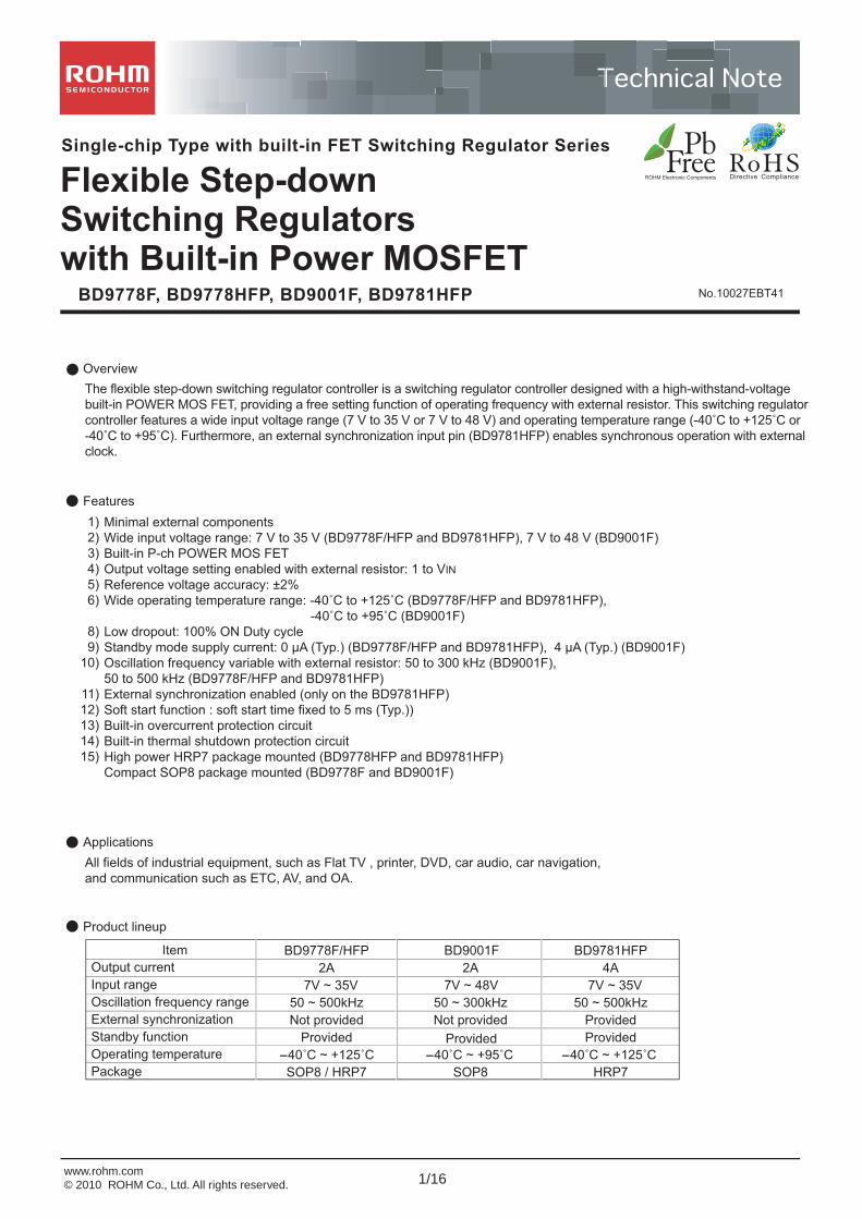
1/16 Single-chip Type with built-in FET Switching Regulator Series Flexible Step-down Switching Regulators with Built-in Power MOSFET BD9778F, BD9778HFP, BD9001F, BD9781HFP www.rohm.com © 2010 ROHM Co., Ltd. All rights reserved. No.10027EBT41 Overview Features 1) 2) 3) 4) 5) 6) 8) 9) 10) 11) 12) 13) 14) 15) Minimal external components Wide input voltage range: 7 V to 35 V (BD9778F/HFP and BD9781HFP), 7 V to 48 V (BD9001F) Built-in P-ch POWER MOS FET Output voltage setting enabled with external resistor: 1 to VIN Reference voltage accuracy: ±2% Wide operating temperature range: -40˚C to +125˚C (BD9778F/HFP and BD9781HFP), -40˚C to +95˚C (BD9001F) Low dropout: 100% ON Duty cycle Standby mode supply current: 0 µA (Typ.) (BD9778F/HFP and BD9781HFP), 4 µA (Typ.) (BD9001F) Oscillation frequency variable with external resistor: 50 to 300 kHz (BD9001F), 50 to 500 kHz (BD9778F/HFP and BD9781HFP) External synchronization enabled (only on the BD9781HFP) Soft start function : soft start time fixed to 5 ms (Typ.)) Built-in overcurrent protection circuit Built-in thermal shutdown protection circuit High power HRP7 package mounted (BD9778HFP and BD9781HFP) Compact SOP8 package mounted (BD9778F and BD9001F) All fields of industrial equipment, such as Flat TV , printer, DVD, car audio, car navigation, and communication such as ETC, AV, and OA. Applications Product lineup The flexible step-down switching regulator controller is a switching regulator controller designed with a high-withstand-voltage built-in POWER MOS FET, providing a free setting function of operating frequency with external resistor. This switching regulator controller features a wide input voltage range (7 V to 35 V or 7 V to 48 V) and operating temperature range (-40˚C to +125˚C or -40˚C to +95˚C). Furthermore, an external synchronization input pin (BD9781HFP) enables synchronous operation with external clock. BD9778F/HFP 2A 7V ~ 35V 50 ~ 500kHz Not provided Provided -40˚C ~ +125˚C SOP8 / HRP7 Output current Input range Oscillation frequency range External synchronization Standby function Operating temperature Package BD9001F 2A 7V ~ 48V 50 ~ 300kHz Not provided Provided -40˚C ~ +95˚C SOP8 BD9781HFP 4A 7V ~ 35V 50 ~ 500kHz Provided Provided -40˚C ~ +125˚C HRP7 Item
Transcript of Single-chip Type with built-in FET Switching Regulator...
1/16
Single-chip Type with built-in FET Switching Regulator Series
Flexible Step-downSwitching Regulators with Built-in Power MOSFET
BD9778F, BD9778HFP, BD9001F, BD9781HFP
www.rohm.com© 2010 ROHM Co., Ltd. All rights reserved.
No.10027EBT41
Overview
Features
1)
2)
3)
4)
5)
6)
8)
9)
10)
11)
12)
13)
14)
15)
Minimal external components
Wide input voltage range: 7 V to 35 V (BD9778F/HFP and BD9781HFP), 7 V to 48 V (BD9001F)
Built-in P-ch POWER MOS FET
Output voltage setting enabled with external resistor: 1 to VIN
Reference voltage accuracy: ±2%
Wide operating temperature range: -40˚C to +125˚C (BD9778F/HFP and BD9781HFP),
-40˚C to +95˚C (BD9001F)
Low dropout: 100% ON Duty cycle
Standby mode supply current: 0 µA (Typ.) (BD9778F/HFP and BD9781HFP), 4 µA (Typ.) (BD9001F)
Oscillation frequency variable with external resistor: 50 to 300 kHz (BD9001F),
50 to 500 kHz (BD9778F/HFP and BD9781HFP)
External synchronization enabled (only on the BD9781HFP)
Soft start function : soft start time fixed to 5 ms (Typ.))
Built-in overcurrent protection circuit
Built-in thermal shutdown protection circuit
High power HRP7 package mounted (BD9778HFP and BD9781HFP)
Compact SOP8 package mounted (BD9778F and BD9001F)
All fields of industrial equipment, such as Flat TV , printer, DVD, car audio, car navigation,
and communication such as ETC, AV, and OA.
Applications
Product lineup
The flexible step-down switching regulator controller is a switching regulator controller designed with a high-withstand-voltage
built-in POWER MOS FET, providing a free setting function of operating frequency with external resistor. This switching regulator
controller features a wide input voltage range (7 V to 35 V or 7 V to 48 V) and operating temperature range (-40˚C to +125˚C or
-40˚C to +95˚C). Furthermore, an external synchronization input pin (BD9781HFP) enables synchronous operation with external
clock.
BD9778F/HFP
2A
7V ~ 35V
50 ~ 500kHz
Not provided
Provided
-40˚C ~ +125˚C
SOP8 / HRP7
Output current
Input range
Oscillation frequency range
External synchronization
Standby function
Operating temperature
Package
BD9001F
2A
7V ~ 48V
50 ~ 300kHz
Not provided
Provided
-40˚C ~ +95˚C
SOP8
BD9781HFP
4A
7V ~ 35V
50 ~ 500kHz
Provided
Provided
-40˚C ~ +125˚C
HRP7
Item
rlwindt301user
タイプライターテキスト
Dec.2015 - Rev.C
rlwindt301user
タイプライターテキスト

2/16
Technical Note
Absolute Maximum Ratings(Ta = 25˚C)
Recommended operating range
Electrical characteristics
*1 Should not exceed Pd-value.
*2 Reduce by 44mW/°C over 25°C, when mounted on 2-layer PCB of 70 X 70 X 1.6 mm3.
(PCB incorporates thermal via. Copper foil area on the front side of PCB: 10.5 X 10.5 mm2. Copper foil area on the reverse side of PCB: 70 X 70 mm2)
*3 Reduce by 5.52 mW/°C over 25°C, when mounted on 2-layer PCB of 70 X 70 X 1.6 mm3.
Output switch pin voltage
Output switch current
BD9778F/HFP,BD9781HFP
BD9778F/HFP,BD9781HFP
BD9778F/HFP, BD9001F
BD9001F
BD9001F
BD9781HFP
HRP7
SOP8Power dissipation
Parameter Symbol Unit
VEN/SYNC,VEN
VRT,VFB,VINV
A
Pd
Limits
5.50.69
VIN
2
EN/SYNC, EN pin voltage VIN
VSW
ISW
50
W
Topr
Tstg
Tjmax
-40 ~ +95-40 ~ +125
-55 ~ +150
˚C
˚C˚C
Power supplyvoltage
Operating temperature range
VIN36
V
V
V
*1
4 *1
*2
*3
RT, FB, INV pin voltage
Storage temperature rangeMaximum junction temperature
7
150
BD9778F/HFP
7 ~ 35
~ 2
6 ~ 100
50 ~ 500
40 ~ 800
Parameter
Operating power supply voltage
Output switch current
Output voltage (ON Duty)
Oscillation frequency
Oscillation frequency set resistance
BD9001F
7 ~ 48
~ 2
6 ~ 100
50 ~ 300
100 ~ 800
BD9781HFP
7 ~ 35
~ 4
6 ~ 100
50 ~ 500
39 ~ 800
Unit
V
A
%
kHz
kΩ
Possible operating range
BD9778F/HFP
5 ~ 35
Parameter
Operating power supply voltage
BD9001F
7 ~ 48
BD9781HFP
5 ~ 35
Unit
V
BD9778F/HFP (Unless otherwise specified, Ta = -40˚C to +125˚C, VIN =13.2 V, VEN = 5 V)
Circuit currentStandby circuit current
Reference voltage 2Reference voltage 1[Error Amp block]
Reference voltage input regulationInput bias currentMaximum FB voltage
ParameterLimitsTyp.Min. Max.
0.96
--
-Operating output current of overcurrent protection 2
-
Symbol
IOLIMIT
IOLEAK
VREF2
VREF1
∆VREF
IQISTB
RON
IBVFBH
VFBL
IFBSINK
IFBSOURCE
TSS
FOSC
VEN
IEN
∆FOSC
-12.4
70
-
-
82-
0.8-
Condition
VEN=5V
VFB=VINV
VFB=1.5V,VINV=1.5VVFB=1.5V,VINV=0.5V
kHz
VIN=5 ~ 35V
VIN=5 ~ 35V
VINV=1.1VVINV=0.5VVINV=1.5V
VIN=35V,VEN=0V
VEN=0V,Ta=25˚CIO=0A
ISW=50mA* Design assurance
* Design assurance
Output leak current
[SW block]POWER MOS FET ON resistance
Minimum FB voltageFB sink currentFB source currentSoft start time[Oscillator block]Oscillation frequencyFrequency input regulation[Enable block]
Threshold voltageSink current
-
-5.0
Unit
AµA
µA
V%
mA
Ω
µAVV
mAµAmS
RT=390kΩ
VµA
%
1.00
3
0.534
0.5-
2.5
120
0.05
5
1021
1.713
0
0
-3.0
1.040.98 VFB=VINV,Ta=25˚CV1.00 1.02
4.210
0.9-
---
170
0.10
-
122-
2.650
30
-0.5
* Not designed to be radiation-resistant.
www.rohm.com© 2010 ROHM Co., Ltd. All rights reserved.
BD9778F, BD9778HFP, BD9001F, BD9781HFP
rlwindt301user
タイプライターテキスト
Dec.2015 - Rev.C

3/16
Technical Note
BD9781HFP (Unless otherwise specified, Ta=-40˚C ~ +125˚C,VIN=13.2V,VEN/SYNC=5V)
Parameter Symbol
IOLIMIT
IOLEAK
VREF2
VREF1
∆VREF
IQISTB
RON
IBVFBH
VFBL
IFBSINK
IFBSOURCE
TSS
FOSC
VEN/SYNC
IEN/SYNC
FSYNC
∆FOSC
ConditionUnit
AµA
V%
mA
Ω
µAVV
mAµAmS
kHz
VµAkHz
%
VEN/SYNC=5V
VEN/SYNC=0V,Ta=25ºC
FEN/SYNC=150kHz
VFB=VINV
VFB=1.5V,VINV=1.5VVFB=1.5V,VINV=0.5V
RT=390kΩ
VIN=5 ~ 35V
VIN=5 ~ 35V
VINV=1.1VVINV=0.5VVINV=1.5V
VIN=35V,VEN/SYNC=0V
IO=0A
ISW=50mA* Design assurance
* Design assurance
[Enable/Synchronizing input block]
Threshold voltageSink currentExternal synchronizing frequency
LimitsTyp.Min. Max.
0.97
-
-4
--12.4
70
-
-
82-
0.8--
-
-5.0
1.00
3
0.58
0.5-
2.5
120
0.05
5
1021
1.735
150
0
-3.0
1.03V VFB=VINV,Ta=25ºC0.98 1.00 1.02
8
0.9-
---
170
0.10
-
122-
2.690-
30
µA- 0 10
-0.5
* Not designed to be radiation-resistant.
Circuit currentStandby circuit current
Reference voltage2Reference voltage1[Error Amp block]
Reference voltage input regulationInput bias currentMaximum FB voltage
Operating output current of overcurrent protectionOutput leak current
[SW block]POWER MOS FET ON resistance
Minimum FB voltageFB sink currentFB source currentSoft start time[Oscillator block]Oscillation frequencyFrequency input regulation
BD9001F (Unless otherwise specified, Ta=-40˚C ~ +95˚C,VIN=13.2V, VEN=5V)
[Enable block]Threshold voltageSink current
Circuit currentStandby circuit current
Reference voltage 2Reference voltage 1[Error Amp block]
Reference voltage input regulationInput bias currentMaximum FB voltage
Parameter
Operating output current of overcurrent protection
VEN
IEN
Symbol
IOLIMIT
VREF2
VREF1
∆VREF
IQISTB
RON
IBVFBH
VFBL
IFBSINK
IFBSOURCE
Tss
FOSC
∆FOSC
Condition
VµA
Unit
A
VV
%
mA
Ω
µA
µA
VV
mA
ms
µA
kHz%
VFB=VINV
VFB=1.5V,VINV=1.5VVFB=1.5V,VINV=0.5V
RT=390kΩ
VIN=7 ~ 48V
VIN=7 ~ 48V
VEN =5V
VINV=1.1VVINV=0.5VVINV=1.5V
IO=0A
ISW=50mA* Design assurance
* Design assurance
[SW block]POWER MOS FET ON resistance
Minimum FB voltageFB sink currentFB source currentSoft start time[Oscillator block]Oscillation frequencyFrequency input regulation
0.8 1.713
2.650
LimitsTyp.Min. Max.
0.960.98
--
-2.5
--12.4
70
-
-
82-
-
-5.0
1.00
3
0.64
0.5-
2.5
1205
0.05
1022
-3.0
1.041.00 1.02
4.24 10
1.2-
---
-170
0.10
122-
-0.5
* Not designed to be radiation-resistant.
VEN=0V,Ta=25˚C
VFB=VINV,Ta=25˚C
www.rohm.com© 2010 ROHM Co., Ltd. All rights reserved.
BD9778F, BD9778HFP, BD9001F, BD9781HFP
rlwindt301user
タイプライターテキスト
Dec.2015 - Rev.C

4/16
Technical Note
Reference data
Fig.1 Output reference voltage vs.
Ambient temprature(All series)
Fig.2 Frequency vs. Ambient
temperature(All series)
Fig.3 Standby current(BD9781HFP)
Fig.5 Standby current(BD9001F) Fig.6 Circuit current(BD9781HFP)
Fig.8 Circuit current(BD9001F) Fig.9 ON resistance VIN=5V(BD9781HFP)
Fig.11 ON resistanceVIN=13.2V (BD9781HFP)
0.980
0.985
0.990
0.995
1.000
1.005
1.010
1.015
1.020
-25-50 0 25 50 75 100
AMBIENT TEMPERATURE : Ta[ ]
RE
FE
RE
NC
E V
OLTA
GE
: V
RE
F[V
]
1250
100
200
300
400
500
600
-25-50 0 25 50 75 100
AMBIENT TEMPERATURE : Ta[ ]
OS
CIL
LA
TIN
G F
RE
QU
EN
CY
: fo
sc[k
Hz]
125
910kΩ
91kΩ
390kΩ
39kΩ
0
1
2
3
4
5
6
7
8
9
10
50 10 15 20 25 30 40
INPUT VOLTAGE : VIN[V]
STA
ND
-BY
CU
RR
EN
T : I
ST
B[µ
A]
35
125
VCC=12V
Istb=0.14µA
25
125
25
–40
-40
Fig.7 Circuit current(BD9778F/HFP)
1
050 10 15 20 25 30 40
INPUT VOLTAGE : VIN[V]
CIR
CU
IT C
UR
RE
NT
: I
CC[m
A]
CIR
CU
IT C
UR
RE
NT
: I
CC[m
A]
35
2
3
4
-40
25
125
-40
25
125
1
050 10 15 20 25 30 40
INPUT VOLTAGE : VIN[V]
CIR
CU
IT C
UR
RE
NT
: I
CC[m
A]
STA
ND
-BY
CU
RR
EN
T : I
ST
B[µ
A]
35
2
3
4
Fig.10 ON resistance VIN=7V (BD9781HFP)
0.0
0.2
0.4
0.6
0.8
1.0
1.2
1.4
1.6
1.8
0.50.0 1.0 1.5 2.0 2.5 3.0 3.5 4.0 4.5OUTPUT CURRENT : IO[A]
FE
T O
N R
ES
ISTA
NC
E : R
ON[Ω
]
Ta=25
Ta=125
Ta=-40
0.0
0.2
0.4
0.6
0.8
1.0
1.2
1.4
1.6
1.8
0.0
0.2
0.4
0.6
0.8
1.0
1.2
1.4
1.6
1.8
0.50.0 1.0 1.5 2.0 2.5 3.0 3.5 4.0 4.5
OUTPUT CURRENT : IO[A]
FE
T O
N R
ES
ISTA
NC
E : R
ON[Ω
]
Ta=25 Ta=125
Ta=-40
4.50.0
0.2
0.4
0.6
0.8
1.0
1.2
1.4
1.6
1.8
0.50.0 1.0 1.5 2.0 2.5 3.0 3.5 4.0OUTPUT CURRENT : IO[A]
FE
T O
N R
ES
ISTA
NC
E : R
ON[Ω
]
Ta=25Ta=125
Ta=-40
Fig.4 Standby current(BD9778F/HFP)
50 10 15 20 25 30 4035
INPUT VOLTAGE : VIN[V] INPUT VOLTAGE : VIN[V]
INPUT VOLTAGE : VIN[V]
0
1
2
3
4
5
6
7
8
9
10
STA
ND
-BY
CU
RR
EN
T : I
ST
B[µ
A]
125
25 -40
VCC=12V
Istb=0.14µA
60
6050403020100
10
20
30
40
50403020100
1
2
3
4
125
-40
25
Fig.12 ON resistance VIN=5V (BD9778F/HFP)
OUTPUT CURRENT : IO[A]
0.50.0 1.0 1.5 2.0 2.5
FE
T O
N R
ES
ISTA
NC
E : R
ON[Ω
]
Ta=-40
Ta=25
Ta=125
www.rohm.com© 2010 ROHM Co., Ltd. All rights reserved.
BD9778F, BD9778HFP, BD9001F, BD9781HFP
rlwindt301user
タイプライターテキスト
Dec.2015 - Rev.C

5/16
Technical Note
OUTPUT CURRENT : IO[A]
10
20
30
40
50
60
70
80
90
100
00 0.5 1.0
CO
NV
ER
SIO
N E
FF
ICIE
NC
Y [%
]
1.5 2.0
5V output 3.3V output
Fig.18 IO vs Efficiency(VIN=12V,f=100kHz)(BD9778F/HFP)
0
1
2
3
4
5
6
OU
TP
UT
VO
LTA
GE
: V
O[V
]
10 2 3 4 5
OUTPUT CURRENT : IO[A]
Ta=25
Ta=125
Ta=-40
Fig.21 Current capacitance(VIN=12V,Vo=5V,f=100kHz)(BD9778F/HFP)
0
1
2
3
4
5
6
10 2 3 4 5 6 7
OUTPUT CURRENT : IO[A]
OU
TP
UT
VO
LTA
GE
: V
O[V
]
Ta=25
Ta=125
Ta=-40
Fig.20 Current capacitance(VIN=12V,Vo=5V,f=100kHz)(BD9781HFP)
0
1
2
3
4
5
6
10 2 3 4 5
OUTPUT CURRENT : IO[A]
OU
TP
UT
VO
LTA
GE
: V
O[V
]
Ta=25
Ta=125
Ta=-40
Fig.22 Current capacitance(VIN=12V,Vo=5V,f=100kHz)(BD9001F)
Fig.16 ON resistance VIN=13.2V (BD9001F)
Fig.19 IO vs Efficiency(VIN=12V,f=100kHz)(BD9001F)
0 0.4 0.8 1.2 1.6 2
OUTPUT CURRENT : IO[A]
CO
NV
ER
SIO
N E
FF
ICIE
NC
Y [%
]
5V output
3.3V output
2.5V output
0.0
0.2
0.4
0.6
0.8
1.0
1.2
1.4
1.6
1.8
0.0
0.2
0.4
0.6
0.8
1.0
1.2
1.4
1.6
1.8
Fig.14 ON resistance VIN=13.2V (BD9778F/HFP) Fig.15 ON resistance VIN=7V (BD9001F)
0.50.0 1.0 1.5 2.0 2.5
OUTPUT CURRENT : IO[A]
FE
T O
N R
ES
ISTA
NC
E : R
ON[Ω
]
Ta=25
Ta=125
Ta=-40
0 0.5 1 1.5 2 2.5
OUTPUT CURRENT : IO[A]
FE
T O
N R
ES
ISTA
NC
E : R
ON
[Ω]
Ta=25
Ta=125
Ta=–40
0.0
0.2
0.4
0.6
0.8
1.0
1.2
1.4
1.6
1.8
Fig.13 ON resistance VIN=7V (BD9778F/HFP)
OUTPUT CURRENT : IO[A]
0.50.0 1.0 1.5 2.0 2.5
FE
T O
N R
ES
ISTA
NC
E : R
ON[Ω
]
Ta=25
Ta=125
Ta=-40
0.0
0.2
0.4
0.6
0.8
1.0
1.2
1.4
1.6
1.8
0 0.5 1 1.5 2 2.5
OUTPUT CURRENT : IO[A]
FE
T O
N R
ES
ISTA
NC
E : R
ON
[Ω]
Ta=25
10
20
30
40
50
60
70
80
90
100
0
Ta=125
Ta=–40
2.5V output1.5V output
10
20
30
40
50
60
70
80
90
100
0
CO
NV
ER
SIO
N E
FF
ICIE
NC
Y [%
]
OUTPUT CURRENT : IO[A]
Fig.17 IO vs Efficiency(VIN=12V,f=200kHz)(BD9781HFP)
0.50.0 1.0 1.5 2.0 2.5 3.0
3.3V output2.5V output
5V output
www.rohm.com© 2010 ROHM Co., Ltd. All rights reserved.
BD9778F, BD9778HFP, BD9001F, BD9781HFP
rlwindt301user
タイプライターテキスト
Dec.2015 - Rev.C

6/16
Technical Note
Block diagram / Application circuit / Pin assignment
(BD9001F)
Fig.26Fig.25
No.
1
2
3
4
5
6
7
FIN
Pin name
VIN
SW
RT
GND
FB
INV
EN/SYNC
-
Fig.23
No.
1
2
3
4
5
6
7
8
Function
Power supply input
Output
Error Amp output
Output voltage feedback
Enable
Frequency setting resistor connection
Ground
Power system power supply input
Pin name
VIN
SW
FB
INV
EN
RT
GND
PVIN
Fig.24
No.
1
2
3
4
5
6
7
FIN
Pin name
VIN
SW
FB
GND
INV
RT
EN
-
(BD9778F)
(BD9781HFP)
(BD9778HFP)
3
Vref
220µF 1µF
33µH
330µF
390kΩ0.1µF
4700pF
10kΩ
23kΩ
1
8
-++
-
+
4
SOFTSTART
OSC
DRIVERLATCH
TSD
-
+
6
2
ON/OFF 5
7
EN
L:OFF
H:ON
VIN
PVIN
INV ERROR AMP
RESET
SW VO
GND
CURRENT LIMIT
Vref
FB RT
PWMCOMPARATOR
VIN
INVSWFBVIN
GNDRT
ENPVIN
ENRT
INVGND
FBSW
VIN
EN/SINCINV
FBGND
RTSW
VIN
150kΩ
3
Vref
1
-++
-
+
5
SOFTSTART
OSC
DRIVERLATCH
TSD
-
+
6
2
ON/OFF 7
4
EN
L:OFF
H:ON
VIN
INV ERROR AMP
RESET
SW VO
GND
CURRENT LIMIT
Vref
FB RT
PWMCOMPARATOR
VIN
220µF 1µF
33µH
330µF
390kΩ0.1µF
4700pF
10kΩ
23kΩ
150kΩ
5
Vref
1
-++
-
+
6
SOFTSTART
OSC
DRIVERLATCH
TSD
-
+
3
2
SYNC
ON/OFF 7
4
EN/SYNC
L:OFF
H:ON
VIN
INV ERROR AMP
RESET
SW
VIN
VO
GND
CURRENT LIMIT
Vref
FB RT
PWMCOMPARATOR
220µF 1µF
33µH
330µF
390kΩ0.1µF
4700pF
10kΩ
23kΩ
150kΩ
Function
Power supply input
Output
Error Amp output
Ground
Output voltage feedback
Frequency setting resistor connection
Enable
Ground
Function
Power supply input
Output
Frequency setting resistor connection
Ground
Error Amp output
Output voltage feedback
Enable/Synchronizing pulse input
Ground
3
VrefSOFT
START
8
-++
-
+
4
OSC
DRIVERLATCH
TSD
-
+
6
1
7
INV ERROR AMP
RESET
SW VO
VIN
GND
CURRENT LIMIT
Vref
VIN
FB RT
PWMCOMPARATOR
INVN.C.FBSW
GNDRT
ENVIN
220µF 1µF
33 µH
330µF
390k0.1µF
4700pF
10k
23k
150k
No.
1
2
3
4
5
6
7
8
Function
Output
Non Connection
Error Amp Output
Output voltage feedback
Enable
Frequency setting resistor connection
Ground
Power supply input
Pin name
SW
N.C.
FB
INV
EN
RT
GND
VIN
www.rohm.com© 2010 ROHM Co., Ltd. All rights reserved.
BD9778F, BD9778HFP, BD9001F, BD9781HFP
rlwindt301user
タイプライターテキスト
Dec.2015 - Rev.C
7/16
Technical Note
Description of operations
ERROR AMP
The ERROR AMP block is an error amplifier used to input the reference voltage (1 V typ.) and the INV pin voltage. The output
FB pin controls the switching duty and output voltage Vo. These INV and FB pins are externally mounted to facilitate phase
compensation. Inserting a capacitor and resistor between these pins enables adjustment of phase margin. (Refer to
recommended examples on page 11.)
SOF T START
The SOFT START block provides a function to prevent the overshoot of the output voltage Vo through gradually increasing
the normal rotation input of the error amplifier when power supply turns ON to gradually increase the switching Duty. The soft
start time is set to 5 msec (Typ.).
ON/OFF(BD9778F/HF P,BD9781HFP)
Setting the EN pin to 0.8 V or less makes it possible to shut down the circuit. Standby current is set to 0 µA (Typ.).
Furthermore, on the BD9781HFP, applying a pulse having a frequency higher than set oscillation frequency to the EN/SYNC
pin allows for external synchronization (up to +50% of the set frequency).
PWM COM PARATOR
The PWM COMPARATOR block is a comparator to make comparison between the FB pin and internal triangular wave and
output a switching pulse.
The switching pulse duty varies with the FB value and can be set in the range of 0 to 100%.
OSC(Oscillator)
The OSC block is a circuit to generate a triangular wave that is to be input in the PWM comparator. Connecting a resistor to
the RT pin enables setting of oscillation frequency.
TSD(Thermal Shut Down)
In order to prevent thermal destruction/thermal runaway of this IC, the TSD block will turn OFF the output when the chip
temperature reaches approximately 150˚C or more. When the chip temperature falls to a specified level, the output will be
reset. However, since the TSD is designed to protect the IC, the chip junction temperature should be provided with the thermal
shutdown detection temperature of less than approximately 150˚C.
CURREN T LIMIT
While the output POWER P-ch MOS FET is ON, if the voltage between drain and source (ON resistance ¥ load current)
exceeds the reference voltage internally set with the IC, this block will turn OFF the output to latch. The overcurrent protection
detection values have been set as shown below:
BD9781HFP . . . 8A(Typ.)
BD9001F,BD9778F/HFP . . . 4A(Typ.)
Furthermore, since this overcurrent protection is an automatically reset, after the output is turned OFF and latched, the latch will
be reset with the RESET signal output by each oscillation frequency.
However, this protection circuit is only effective in preventing destruction from sudden accident. It does not support for the
continuous operation of the protection circuit (e.g. if a load, which significantly exceeds the output current capacitance, is
normally connected). Furthermore, since the overcurrent protection detection value has negative temperature characteristics,
consider thermal design.
www.rohm.com© 2010 ROHM Co., Ltd. All rights reserved.
BD9778F, BD9778HFP, BD9001F, BD9781HFP
rlwindt301user
タイプライターテキスト
Dec.2015 - Rev.C

8/16
Technical Note
Timing chart
(BD9781HFP)
- While in basic operation mode
- While in overcurrent protection mode
FB
VIN
SW
EN/SYNC
Internal
OSC
Fig.27
Fig.28
External synchronizing function (BD9781HFP)
In order to activate the external synchronizing function, connect the frequency setting resistor to the RT pin and then input
a synchronizing signal to the EN/SYNC pin. As the synchronizing signal, input a pulse wave higher than a frequency determined
with the setting resistor (RT). On the BD9781HFP, design the frequency difference to be within 50%. Furthermore,
set the pulse wave duty between 10% and 90%.
Fig.29
FSYNC
Internal
OSC
: For RT only
: For external
synchronization
Output short circuit
FB
SW
IO
Internal
OSC
Auto reset Auto reset Auto reset Auto reset
www.rohm.com© 2010 ROHM Co., Ltd. All rights reserved.
BD9778F, BD9778HFP, BD9001F, BD9781HFP
rlwindt301user
タイプライターテキスト
Dec.2015 - Rev.C

9/16
Technical Note
Description of external components
Design procedure Calculation example
Vo = Output voltage, Vin (Max.) = Maximum input voltage
Io (Max.) = Maximum load current, f = Oscillation frequency
1. Setting or output voltage
Output voltage can be obtained by the formula shown below.
VO=1 x (1+R1/R2)
Use the formula to select the R1 and R2.
Furthermore, set the R2 to 30 kΩ or less.
Select the current passing through the R1 and R2 to be small
enough for the output current.
2. Selection of coil (L)
The value of the coil can be obtained by the formula shown
below:
L=(VIN-VO) x VO / (VIN x f x ∆IO)
∆IO: Output ripple current
f = Operating frequency
∆Io should typically be approximately 20 to 30% of Io.
3. Selection of output capacitor (Co)
The output capacitor can be determined according to the
output ripple voltage ∆Vo (p-p) required.
Obtain the required ESR value by the formula shown below
and then select the capacitance.
When VIN = 13.2 V, Vo = 5 V, Io = 2 A, and f = 100 kHz,
L=(13.2-5) x 5/13.2 x 1/100k x 1/(2 x 0.3)
=51.8µH 47µ
VIN=13.2V, Vo=5V, L=100µH, f=100kHz
∆IL=(13.2-5) x 5/(100 x 10-6 x 100 x 103 x 13.2)
0.31
When Vo = 5 V and R2 = 10 kΩ ,
5=1 x (1+R1/10kΩ)
R1=40kΩ
L=47µH
Fig.30
VIN
RT
SS
SW
INV
FB
GND
CT
Cin Di CO
+
VOVIN
CC RC
C
L
R1
R2RT
CSS
3.5m x (ILimit-Io(Max))
VoCMax=
CMax=3.5m x (2-1)/5
=700µ
∆IL=0.31A
CMax=700µF
If this coil is not set to the optimum value, normal (continuous)
oscillation may not be achieved. Furthermore, set the value of
the coil with an adequate margin so that the peak current passing
through the coil will not exceed the rated current of the coil.
ILimit:2A(BD9778F/HFP,BD9001F), 4A(BD9781HFP)
If this capacitance is not optimum, faulty startup may result.
( 3.5m is soft start time(min.))
When ILimit: 2 A, Io (Max) = 1 A, and Vo = 5V,
∆IL=(VIN-VO) x VO/(L x f x VIN)
∆Vpp=∆IL x ESR+(∆IL x Vo)/(2 x Co x f x VIN)
Set the rating of the capacitor with an adequate margin to the
output voltage. Also, set the maximum allowable ripple current
with an adequate margin to ∆IL. Furthermore, the output rise
time should be shorter than the soft start time. Select the output
capacitor having a value smaller than that obtained by the
formula shown below.
www.rohm.com© 2010 ROHM Co., Ltd. All rights reserved.
BD9778F, BD9778HFP, BD9001F, BD9781HFP
rlwindt301user
タイプライターテキスト
Dec.2015 - Rev.C

10/16
Technical Note
Design procedure Calculation example
4. Selection of diode
When VIN = 36 V and Io = (max.) 2 A,
When VIN = 13.2 V, Vo = 5 V, and Io = 1 A,
IRMS=1 X 5 X (13.2-5)/(13.2)2
=0.485
5. Selection of input capacitor
6. Setting of oscillation frequency
7. Setting of phase compensation (Rc and Cc)
Directions for pattern layout of PCB
* The set values listed above are all reference values. On the actual mounting of the IC, the characteristics may vary with the routing of wirings
and the types of parts in use. In this connection, it is recommended to thoroughly verify these values on the actual system prior to use.
IRMS=0.485A
Set diode rating with an adequate margin to the maximum load
current. Also, make setting of the rated inverse voltage with
an adequate margin to the maximum input voltage.
A diode with a low forward voltage and short reverse recovery
time will provide high efficiency.
Select a diode of rated current of 2 A or more and rated
withstand voltage of 36 V or more.
Two capacitors, ceramic capacitor CIN and bypass capacitor C,
should be inserted between the VIN and GND.Be sure to insert
a ceramic capacitor of 1 to 10 µF for the C. The capacitor C
should have a low ESR and a significantly large ripple current.
The ripple current IRMS can be obtained
by the following formula:
Select capacitors that can accept this ripple current.
If the capacitance of CIN and C is not optimum,
the IC may malfunction.
IRMS=IO X VO X (Vin-VO)/ Vin2
Referring Fig. 34 and Fig. 35 on the following page, select R
for the oscillation frequency to be used. Furthermore,
in order to eliminate noises, be sure to connect ceramic
capacitors of 0.1 to 1.0 µF in parallel.
The phase margin can be set through inserting a capacitor or
a capacitor and resistor between the INV pin and the FB pin.
Each set value varies with the output coil, capacitance,
I/O voltage, and load. Therefore, set the phase compensation
to the optimum value according to these conditions.
(For details, refer to Application circuit on page 11.)
If this setting is not optimum, output oscillation may result.
Fig.31
1
2
4
3
8
8
6
5
VIN
SW
C
Co
R3
C3
RT CT
Cin
R1
R2
SIGNAL GND
Cx2
Cx1
L
GND
FB
GN
D
GND
INV
RT
EN
BD9778HFP
LOAD
www.rohm.com© 2010 ROHM Co., Ltd. All rights reserved.
BD9778F, BD9778HFP, BD9001F, BD9781HFP
rlwindt301user
タイプライターテキスト
Dec.2015 - Rev.C

11/16
Technical Note
Phase compensation setting procedure
RFeedback
C
FB
-
+
A
(1) Typical integrator (Low pass filter) (2) Open loop characteristics of integrator
0
A
0
-90
-90˚
-180˚-180
Phase
[˚]
Gain
[dB]
f
f
GBW(b)
-20dB/decade
Phase margin
(a)
The following section describes the stability conditions of the negative feedback system.
Since the DC/DC converter application is sampled according to the switching frequency, GBW (frequency at 0-dB gain)
of the overall system should be set to 1/10 or less of the switching frequency. The following section summarizes the targeted
characteristics of this application.
At a 1 (0-dB) gain, the phase delay is 150˚ or less (i.e., the phase margin is 30˚ or more).
The GBW for this occasion is 1/10 or less of the switching frequency.
Responsiveness is determined with restrictions on the GBW. To improve responsiveness, higher switching frequency
should be provided.
Replace a secondary phase delay (-180˚) with a secondary phase lead by inserting two phase leads, to ensure the stability
through the phase compensation. Furthermore, the GBW (i.e., frequency at 0-dB gain) is determined according to phase
compensation capacitance provided for the error amplifier. Consequently, in order to reduce the GBW,
increase the capacitance value.
1. Application stability conditions
Since the error amplifier is provided with (1) or (2) phase compensation, the low pass filter is applied. In the case of
the DC/DC converter application, the R becomes a parallel resistance of the feedback resistance.
Fig.35 RT vs fOSC BD9001F
50
100
150
200
250
300
10050 200 300 400 500 600 700 800
OSCILATING FREQUENCY SETTING RESISTANCE : RT [kΩ]O
SC
ILA
TIN
G F
RE
QU
EN
CY
: fosc[k
Hz]
Fig.34 RT vs fOSC (BD9781HFP/BD9778F/HFP)
80050
100
150
200
250
300
350
400
450
500
1000 200 300 400 500 600 700
OSCILATING FREQUENCY SETTING RESISTANCE : RT[kΩ]
OS
CIL
AT
ING
FR
EQ
UE
NC
Y : fosc[k
Hz]
Fig.32 BD9001F reference layout pattern Fig.33 BD9781HFP reference layout pattern
As shown above, design the GND pattern as large area as possible
within inner layer.
Gray zones indicate GND.
Co
L
C
Cin
Di
RT
R3
Cx1
R1
C3
Cx2
R2
CT
Co
L
C
Cin
Di Cx1
R3
C3
Cx2
R2
R1RT
CT
www.rohm.com© 2010 ROHM Co., Ltd. All rights reserved.
BD9778F, BD9778HFP, BD9001F, BD9781HFP
rlwindt301user
タイプライターテキスト
Dec.2015 - Rev.C

12/16
Technical Note
L
C+
VCC
VOL
RESR
C
VCC
VO
(1) LC resonant circuit (2) With ESR provided
fr = 1 [Hz]
At this resonance point, a -180˚
A -90˚ phase-delay occurs.
phase-delay occurs.
(3) Insert feedback resistance in the C. (4) Insert the R3 in integrator.
C1VO
R1
R2
C2
FBINV
-
+ A
VO
R1
R2
R3C2
FBINV
-
+ A
3. For output capacitors having low ESR, such as low impedance electrolyte capacitor or OS-CON
(1) Phase compensation with secondary phase lead
VO
R1 C1
R2
R3C2
FBINV
-
+ A
For output capacitors that have high ESR (i.e., several Ω), the phase compensation setting procedure becomes
comparatively simple. Since the DC/DC converter application has a LC resonant circuit attached to the output, a -180˚
phase-delay occurs in that area. If ESR component is present, howeve r, a +90˚ phase-lead occurs to shift the phase
delay to -90˚. Since the phase delay should be set within 150˚, it is a very effective method but tends to increase
the ripple component of the output voltage.
To cancel the LC resonance, the frequency to insert the phase lead should be set close to the LC resonant frequency.
The settings above have are estimated. Consequently, the settings may be adjusted on the actual system. Furthermore,
since these characteristics vary with the layout of PCB loading conditions, precise calculations should be made on the
actual system.
In order to use capacitors with low ESR (i.e., several tens of mΩ), two phase-leads should be inserted so that a -180˚
phase-delay, due to LC resonance, will be compensated. The following section shows a typical phase compensation
procedure.
To set phase lead frequency, insert both of the phase leads close to the LC resonant frequency. According to empirical rule,
setting the phase lead frequency f Z2 with R3 and C2 lower than the LC resonant frequency fr, and the phase lead frequency
fZ1 with the R1 and C1 higher than the LC resonant frequency fr, will provide stable application conditions.
According to changes in phase characteristics, due to the ESR, only one phase lead should be inserted.
For this phase lead, select either of the methods shows below:
2. For output capacitors having high ESR, such as electrolyte capacitor
( )
www.rohm.com© 2010 ROHM Co., Ltd. All rights reserved.
BD9778F, BD9778HFP, BD9001F, BD9781HFP
rlwindt301user
タイプライターテキスト
Dec.2015 - Rev.C

13/16
Technical Note
<Procedure>
1. Check to ensure output causes no oscillation at the maximum
load in closed loop.
Isolate (1) and (2) and insert Vm (with amplitude of
approximately 100 mVpp).
Measure (probe) the oscillation of (1) to that of (2).
2.
3.
Heat loss
Furthermore, the phase margin can also be measured with the
load responsiveness.
Measure variations in the output voltage when instantaneously
changing the load from no load to the maximum load.
Even though ringing phenomenon is caused, due to low phase margin,
no ringing takes place. Phase margin is provided. However,
no specific phase margin can be probed.
To measure the open loop of DC/DC converter, use the gain phase analyzer or FRA to measure the frequency
characteristics.
r A
<Reference> Measurement of open loop of DC/DC converter
The heat loss W of the IC can be obtained by the formula shown below:
W=Ron X Io2 X + VIN X ICC + Tr X VIN X Io X f
Ron: ON resistance of IC (refer to pages 4 and 5.) Io: Load current Vo: Output voltage
VIN: Input voltage Icc: Circuit current (Refer to pages 2 and 3)
Tr: Switching rise/fall time (Approximately 40 nsec)
f : Oscillation frequency
Vo
VIN
1 Ron X Io2
2 2 X
=Tr X VIN X Io X f
X Tr X X VIN X Io21
T1
1Tr
VIN
GND
SW
waveform
T = f1
2
VO
Vm+
RL~
DC/DC converter
controller
Load
Output voltage
Maximum load
t
Adequate phase margin
Inadequate phase margin
0
ºCºC
www.rohm.com© 2010 ROHM Co., Ltd. All rights reserved.
BD9778F, BD9778HFP, BD9001F, BD9781HFP
rlwindt301user
タイプライターテキスト
Dec.2015 - Rev.C
14/16
Technical Note
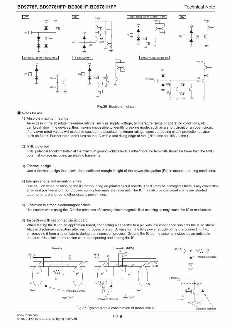
Fig.36 Equivalent circuit
Fig.37 Typical simple construction of monolithic IC
P layer
E
B
C(Pin B)
Transistor (NPN)
P
N
N
N
N
GNDParasitic element
GND
P+ P+
(Pin A)
GND
Parasitic element
(PIN B)
GND
B
E
C
Parasitic element
P+
P layer
(Pin A)
Resistor
P
N
N
N
GND
Parasitic element
P+
Notes for use
1) Absolute maximum ratings
An excess in the absolute maximum ratings, such as supply voltage, temperature range of operating conditions, etc.,
can break down the devices, thus making impossible to identify breaking mode, such as a short circuit or an open circuit.
If any over rated values will expect to exceed the absolute maximum ratings, consider adding circuit protection devices,
such as fuses. Furthermore, don't turn on the IC with a fast rising edge of VIN. ( rise time << 10V / µsec )
2) GND potential
GND potential should maintain at the minimum ground voltage level. Furthermore, no terminals should be lower than the GND
potential voltage including an electric transients.
3) Thermal design
Use a thermal design that allows for a sufficient margin in light of the power dissipation (Pd) in actual operating conditions.
4) Inter-pin shorts and mounting errors
Use caution when positioning the IC for mounting on printed circuit boards. The IC may be damaged if there is any connection
error or if positive and ground power supply terminals are reversed. The IC may also be damaged if pins are shorted
together or are shorted to other circuits power lines.
5) Operation in strong electromagnetic field
Use caution when using the IC in the presence of a strong electromagnetic field as doing so may cause the IC to malfunction.
6) Inspection with set printed circuit board
When testing the IC on an application board, connecting a capacitor to a pin with low impedance subjects the IC to stress.
Always discharge capacitors after each process or step. Always turn the IC's power supply off before connecting it to,
or removing it from a jig or fixture, during the inspection process. Ground the IC during assembly steps as an antistatic
measure. Use similar precaution when transporting and storing the IC.
VIN
EN/SYNC
222kΩ
221kΩ
2kΩ
VREGA
139kΩ
145kΩ
SW
SW
EN
VIN
10kΩ
300kΩ
250kΩ
VIN
2kΩ
300kΩ
50kΩ
RT
VIN
VREF
VIN
EN/SYNC BD9781HFPEN BD9778F/HFP, BD9001F
1kΩ
VIN
FB
VREF
1kΩINV
VIN
VREF
FB BD9778F/HFP, BD9781HFP INVRT
FB BD9001F
1kΩ
VIN
FB
VREF
1kΩ
www.rohm.com© 2010 ROHM Co., Ltd. All rights reserved.
BD9778F, BD9778HFP, BD9001F, BD9781HFP
rlwindt301user
タイプライターテキスト
Dec.2015 - Rev.C

15/16
Technical Note
Thermal derating characteristics
Fig.39 Fig.40
10) On the application shown below, if there is a mode in which VIN and each pin potential are inverted, for example,
if the VIN is short-circuited to the Ground with external diode charged, internal circuits may be damaged. To avoid damage,
it is recommended to insert a backflow prevention diode in the series with VIN or a bypass diode between each pin and VIN.
Fig.35
Pin
Backflow prevention diode
Bypass diode
Vcc
8) Ground wiring pattern
It is recommended to separate the large-current GND pattern from the small-signal GND pattern and establish a single
ground at the reference point of the set PCB, so that resistance to the wiring pattern and voltage fluctuations due to
a large current will cause no fluctuations in voltages of the small-signal GND. Prevent fluctuations in the GND wiring pattern
of external parts.
9) Temperature protection (thermal shut down) circuit
This IC has a built-in temperature protection circuit to prevent the thermal destruction of the IC. As described above,
be sure to use this IC within the power dissipation range. Should a condition exceeding the power dissipation range continue,
the chip temperature Tj will rise to activate the temperature protection circuit, thus turning OFF the output power element.
Then, when the tip temperature Tj falls, the circuit will be automatically reset. Furthermore, if the temperature protection
circuit is activated under the condition exceeding the absolute maximum ratings, do not attempt to use the temperature
protection circuit for set design.
Single piece of IC
PCB size: 70 x 70 x 1.6 mm3 (PCB incorporates thermal via.)
Copper foil area on the front side of PCB: 10.5 x 10.5 mm2
2-layer PCB (Copper foil area on the reverse side of PCB: 15 x 15 mm2)
2-layer PCB (Copper foil area on the reverse side of PCB: 70 x 70 mm2)
4-layer PCB (Copper foil area on the reverse side of PCB: 70 x 70 mm2)
Single piece of IC
When mounted on ROHM standard PCB
(Glass epoxy PCB of 70 mm x 70 mm x 1.6 mm)
10
9
8
7
6
5
4
3
2
1
0
7.3W
5.5W
2.3W
1.4W
25 50 75
HRP7
100 125 150
0.8
0.7
0.6
0.5
0.4
0.3
0.2
0.1
0250 50 75
SOP8
100 125 150
PD
[ W]
PD
[ W]
BD9778FBD9001F
BD9778F, BD9778HFP, BD9001F, BD9781HFP
www.rohm.com© 2010 ROHM Co., Ltd. All rights reserved.
7) IC pin input (Fig. 37)
This monolithic IC contains P+ isolation and P substrate layers between adjacent elements to keep them isolated.
P-N junctions are formed at the intersection of these P layers with the N layers of other elements, creating a parasitic diode
or transistor. For example, the relation between each potential is as follows:
When GND > Pin A and GND > Pin B, the P-N junction operates as a parasitic diode.
When Pin B > GND > Pin A, the P-N junction operates as a parasitic transistor. Parasitic diodes can occur inevitably in the
structure of the IC. The operation of parasitic diodes can result in mutual interference among circuits, operational faults,
or physical damage. Accordingly, methods by which parasitic diodes operate, such as applying a voltage that is lower than
the GND (P substrate) voltage toan input pin, should not be used.
rlwindt301user
タイプライターテキスト
Dec.2015 - Rev.C

16/16
Technical Note
Selection of order type
Package
F = SOP8
HFP = HRP7
Taping type
E2 = Reel-type embossed carrier tape (SOP8)
TR = Reel-type embossed carrier tape (HRP7)
SOP8
HRP7
BD9778F, BD9778HFP, BD9001F, BD9781HFP
www.rohm.com© 2010 ROHM Co., Ltd. All rights reserved.
B D 9 7 7 8 H F P - T R
Part No.9778 = 36V/2A
9781 = 36V/4A
9001 = 50V/2A
Part No.
∗ Order quantity needs to be multiple of the minimum quantity.
<Tape and Reel information>
Embossed carrier tapeTape
Quantity
Direction of feed The direction is the 1pin of product is at the upper left when you hold
reel on the left hand and you pull out the tape on the right hand
2500pcs
E2
( )
Direction of feed
Reel1pin
Direction of feed
1pin
Reel ∗ Order quantity needs to be multiple of the minimum quantity.
<Tape and Reel information>
Embossed carrier tapeTape
Quantity
Direction of feed The direction is the 1pin of product is at the upper right when you hold
reel on the left hand and you pull out the tape on the right hand
2000pcs
TR
( )
rlwindt301user
スタンプ
rlwindt301user
スタンプ
rlwindt301user
タイプライターテキスト
Dec.2015 - Rev.C

DatasheetDatasheet
Notice-PAB-E Rev.002© 2015 ROHM Co., Ltd. All rights reserved.
Notice Precaution on using ROHM Products
1. If you intend to use our Products in devices requiring extremely high reliability (such as medical equipment (Note 1), aircraft/spacecraft, nuclear power controllers, etc.) and whose malfunction or failure may cause loss of human life, bodily injury or serious damage to property (“Specific Applications”), please consult with the ROHM sales representative in advance. Unless otherwise agreed in writing by ROHM in advance, ROHM shall not be in any way responsible or liable for any damages, expenses or losses incurred by you or third parties arising from the use of any ROHM’s Products for Specific Applications.
(Note1) Medical Equipment Classification of the Specific Applications JAPAN USA EU CHINA
CLASSⅢ CLASSⅢ
CLASSⅡb CLASSⅢ
CLASSⅣ CLASSⅢ
2. ROHM designs and manufactures its Products subject to strict quality control system. However, semiconductor
products can fail or malfunction at a certain rate. Please be sure to implement, at your own responsibilities, adequate safety measures including but not limited to fail-safe design against the physical injury, damage to any property, which a failure or malfunction of our Products may cause. The following are examples of safety measures:
[a] Installation of protection circuits or other protective devices to improve system safety [b] Installation of redundant circuits to reduce the impact of single or multiple circuit failure
3. Our Products are not designed under any special or extraordinary environments or conditions, as exemplified below. Accordingly, ROHM shall not be in any way responsible or liable for any damages, expenses or losses arising from the use of any ROHM’s Products under any special or extraordinary environments or conditions. If you intend to use our Products under any special or extraordinary environments or conditions (as exemplified below), your independent verification and confirmation of product performance, reliability, etc, prior to use, must be necessary:
[a] Use of our Products in any types of liquid, including water, oils, chemicals, and organic solvents [b] Use of our Products outdoors or in places where the Products are exposed to direct sunlight or dust [c] Use of our Products in places where the Products are exposed to sea wind or corrosive gases, including Cl2,
H2S, NH3, SO2, and NO2
[d] Use of our Products in places where the Products are exposed to static electricity or electromagnetic waves [e] Use of our Products in proximity to heat-producing components, plastic cords, or other flammable items [f] Sealing or coating our Products with resin or other coating materials [g] Use of our Products without cleaning residue of flux (even if you use no-clean type fluxes, cleaning residue of
flux is recommended); or Washing our Products by using water or water-soluble cleaning agents for cleaning residue after soldering
[h] Use of the Products in places subject to dew condensation
4. The Products are not subject to radiation-proof design. 5. Please verify and confirm characteristics of the final or mounted products in using the Products. 6. In particular, if a transient load (a large amount of load applied in a short period of time, such as pulse. is applied,
confirmation of performance characteristics after on-board mounting is strongly recommended. Avoid applying power exceeding normal rated power; exceeding the power rating under steady-state loading condition may negatively affect product performance and reliability.
7. De-rate Power Dissipation depending on ambient temperature. When used in sealed area, confirm that it is the use in
the range that does not exceed the maximum junction temperature. 8. Confirm that operation temperature is within the specified range described in the product specification. 9. ROHM shall not be in any way responsible or liable for failure induced under deviant condition from what is defined in
this document.
Precaution for Mounting / Circuit board design 1. When a highly active halogenous (chlorine, bromine, etc.) flux is used, the residue of flux may negatively affect product
performance and reliability. 2. In principle, the reflow soldering method must be used on a surface-mount products, the flow soldering method must
be used on a through hole mount products. If the flow soldering method is preferred on a surface-mount products, please consult with the ROHM representative in advance.
For details, please refer to ROHM Mounting specification

DatasheetDatasheet
Notice-PAB-E Rev.002© 2015 ROHM Co., Ltd. All rights reserved.
Precautions Regarding Application Examples and External Circuits 1. If change is made to the constant of an external circuit, please allow a sufficient margin considering variations of the
characteristics of the Products and external components, including transient characteristics, as well as static characteristics.
2. You agree that application notes, reference designs, and associated data and information contained in this document
are presented only as guidance for Products use. Therefore, in case you use such information, you are solely responsible for it and you must exercise your own independent verification and judgment in the use of such information contained in this document. ROHM shall not be in any way responsible or liable for any damages, expenses or losses incurred by you or third parties arising from the use of such information.
Precaution for Electrostatic
This Product is electrostatic sensitive product, which may be damaged due to electrostatic discharge. Please take proper caution in your manufacturing process and storage so that voltage exceeding the Products maximum rating will not be applied to Products. Please take special care under dry condition (e.g. Grounding of human body / equipment / solder iron, isolation from charged objects, setting of Ionizer, friction prevention and temperature / humidity control).
Precaution for Storage / Transportation 1. Product performance and soldered connections may deteriorate if the Products are stored in the places where:
[a] the Products are exposed to sea winds or corrosive gases, including Cl2, H2S, NH3, SO2, and NO2 [b] the temperature or humidity exceeds those recommended by ROHM [c] the Products are exposed to direct sunshine or condensation [d] the Products are exposed to high Electrostatic
2. Even under ROHM recommended storage condition, solderability of products out of recommended storage time period may be degraded. It is strongly recommended to confirm solderability before using Products of which storage time is exceeding the recommended storage time period.
3. Store / transport cartons in the correct direction, which is indicated on a carton with a symbol. Otherwise bent leads
may occur due to excessive stress applied when dropping of a carton. 4. Use Products within the specified time after opening a humidity barrier bag. Baking is required before using Products of
which storage time is exceeding the recommended storage time period.
Precaution for Product Label QR code printed on ROHM Products label is for ROHM’s internal use only.
Precaution for Disposition When disposing Products please dispose them properly using an authorized industry waste company.
Precaution for Foreign Exchange and Foreign Trade act Since concerned goods are fallen under listed items of export control prescribed by Foreign exchange and Foreign trade act, the permission based on the act is necessary in case of export.
Precaution Regarding Intellectual Property Rights 1. All information and data including but not limited to application example contained in this document is for reference
only. ROHM does not warrant that foregoing information or data will not infringe any intellectual property rights or any other rights of any third party regarding such information or data.
2. ROHM shall not have any obligations where the claims, actions or demands arising from the combination of the Products with other articles such as components, circuits, systems or external equipment (including software).
3. No license, expressly or implied, is granted hereby under any intellectual property rights or other rights of ROHM or any third parties with respect to the Products or the information contained in this document. Provided, however, that ROHM will not assert its intellectual property rights or other rights against you or your customers to the extent necessary to manufacture or sell products containing the Products, subject to the terms and conditions herein.
Other Precaution 1. This document may not be reprinted or reproduced, in whole or in part, without prior written consent of ROHM.
2. The Products may not be disassembled, converted, modified, reproduced or otherwise changed without prior written consent of ROHM.
3. In no event shall you use in any way whatsoever the Products and the related technical information contained in the Products or this document for any military purposes, including but not limited to, the development of mass-destruction weapons.
4. The proper names of companies or products described in this document are trademarks or registered trademarks of ROHM, its affiliated companies or third parties.

DatasheetDatasheet
Notice – WE Rev.001© 2015 ROHM Co., Ltd. All rights reserved.
General Precaution 1. Before you use our Pro ducts, you are requested to care fully read this document and fully understand its contents.
ROHM shall n ot be in an y way responsible or liabl e for fa ilure, malfunction or acci dent arising from the use of a ny ROHM’s Products against warning, caution or note contained in this document.
2. All information contained in this docume nt is current as of the issuing date and subj ect to change without any prior
notice. Before purchasing or using ROHM’s Products, please confirm the la test information with a ROHM sale s representative.
3. The information contained in this doc ument is provi ded on an “as is” basis and ROHM does not warrant that all
information contained in this document is accurate an d/or error-free. ROHM shall not be in an y way responsible or liable for any damages, expenses or losses incurred by you or third parties resulting from inaccuracy or errors of or concerning such information.