
SIMULATION OF PERIODIC NANOSTRUCTURES FOR...
34
SIMULATION OF PERIODIC NANOSTRUCTURES FOR DESIGN AND OPTIMIZATION OF PLASMONIC BIOSENSORS Niccolò Michieli CNISM and Department of Physics and Astronomy «G.Galilei» - University of Padua Nanostructures Group
Transcript of SIMULATION OF PERIODIC NANOSTRUCTURES FOR...

SIMULATION OF PERIODIC
NANOSTRUCTURES FOR DESIGN AND
OPTIMIZATION OF PLASMONIC BIOSENSORS
Niccolò Michieli
CNISM and Department of Physics and Astronomy «G.Galilei» - University
of Padua
Nanostructures Group

LIGHT-MATTER INTERACTION BIOSENSORS
PLASMONICS
• Biosensor => transduce biological (and chemical) signal into
a set of useable informations (composition, concentration...)
• Light-matter interactions are the main physical
phenomena exploited to this aim.
• Particularly, Nanotechnology and Nanoscience
can yield important advantages:
• size of analytes: 0.1-1000 nm
• energetic and roto-vibrational transitions => nanometric wavelenghts
• optical technology, sources and detectors
• (noble) metals nanostructures support coherent
free charges oscillations

LIGHT-MATTER INTERACTION BIOSENSORS
Biosensors
Labeled
SERS
Hot Spots
Fluorescence
Light Management
Specific Absorption
Light Management
...
Label-free
Refractive index
Localized Plasmons
Surface Plasmos
Surface modification
...
Nanotriangles Nanoholes

PLASMONICS – SURFACE AND LOCALIZED
PLASMONS
Plasmons
Surface Plasmons Localized Plasmons
• Propagating modes
• Coupling by prism or grating
• Poor Field Confinement
• Low absorption
• Extremely sensitive to
surrounding index changes
• Confined modes
• Direct coupling
• Strong Field Confinement
• High absorption
• Extremely sensitive to
(geometrically) small changes
in surround

SURFACE PLASMON POLARITONS
• Wave equation (Helmhotz’s Equation) at metal-dielectric interface:
𝜕2𝑬(𝑧)
𝜕𝑧2 + 𝑘02𝜀 − 𝑘𝑥
2 𝑬 = 𝟎
• Putting the Boundary Conditions, the dispersion relation results:
𝑘𝑥 = 𝑘0
𝜀1𝜀2
𝜀1 + 𝜀2
• Direct coupling forbidden!!
• Coupling methods:
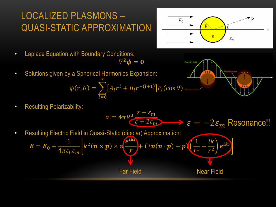
LOCALIZED PLASMONS –
QUASI-STATIC APPROXIMATION
• Laplace Equation with Boundary Conditions:
𝛻𝟐𝝓 = 𝟎
• Solutions given by a Spherical Harmonics Expansion:
𝜙 𝑟, 𝜃 = 𝐴𝑙𝑟𝑙 + 𝐵𝑙𝑟
− 𝑙+1 𝑃𝑙 cos 𝜃
∞
𝑙=0
• Resulting Polarizability:
𝛼 = 4𝜋𝑅3𝜀 − 𝜀𝑚
𝜀 + 2𝜀𝑚
• Resulting Electric Field in Quasi-Static (dipolar) Approximation:
𝑬 = 𝑬𝟎 +1
4𝜋𝜀0𝜀𝑚𝑘2 𝒏 × 𝒑 × 𝒏
𝒆𝒊𝒌𝒓
𝒓+ 3𝒏 𝒏 ∙ 𝒑 − 𝒑
1
𝑟3 −𝑖𝑘
𝑟2 𝒆𝒊𝒌𝒓
𝜀 = −2𝜀𝑚 Resonance!!
Far Field Near Field

BEYOND QUASI-STATIC APPROXIMATIONS
Exact solutions of the electromagnetic problem only exists for a few particular cases:
• Spherical isolated particles: Mie theory
Multipole expansion (quadrupoles, ottupoles,...)
• Ellipsoidal particles: Gans theory
• Spherical interacting particles: Generalized Multiparticle Mie (GMM)
For all other geometries: Discretization (DDA, FEM, FDFD, FDTD)
Typical observed features:
500 600 700 800 900 10000
2
4
6
8
10
12
14
Extin
ctio
n E
ffic
ien
cy
Wavelength (nm)
46 48 50 52 54 56 58 60 620.0
0.1
0.2
0.3
0.4
0.5
0.6
Re
fle
cta
nce
Angle (°)

HOW TO EXPLOIT PLASMONICS FOR
BIOSENSORS?
Sensors
SERS
Hot Spots
Transmission/
Extinction
Resonances
Peaks
Reflection
Propagating Modes
Nanohole Arrays Nano Triangles

NANOSTRUCTURES SELF-ASSEMBLY - NSL 2a.
1. SiO2 NS (30-1000 nm)
Nano Triangles

NANOSTRUCTURES SELF-ASSEMBLY - NSL 2a.
1. SiO2 NS (30-1000 nm)
2b.
Nano Triangles
Nano Hole Arrays

2D PERIODIC STRUCTURES: THE HONEYCOMB
LATTICE
All the structures taken in count are periodic, with a «honeycomb» lattice.
• The lattice can be decomposed in triangles or in exagons.
• It can be seen as a sinlge plane of a HCP crystal.
• The unit cell is a rhomb, which is one third of the unitary
exagon and is composed by two unit triangles.
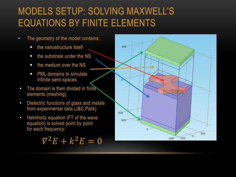
MODELS SETUP: SOLVING MAXWELL’S
EQUATIONS BY FINITE ELEMENTS
• The geometry of the model contains:
the nanostructure itself
the substrate under the NS
the medium over the NS
PML domains to simulate infinite semi-spaces.
• The domain is then divided in finite elements (meshing)
• Dielectric functions of glass and metals from experimental data (J&C,Palik)
• Helmholtz equation (FT of the wave equation) is solved point by point for each frequency:
𝛻2𝐸 + 𝑘2𝐸 = 0

NANOTRIANGLES
• The unit cell contains 2 nanotriangles. These are placed in the
centers of the two triangles forming the unit cell.
• The tips of tips of the triangles are faced each-other.
• The exact shape of the monomer is determined by the technique
of deposition, the quantity of deposed metal, and by (optional)
thermal annealing.
• Nanostructures have been modelized both as snipped prisms
and snipped thetrahedra.

NANOTRIANGLES – RESONANCE TAYLORING
The resonance position (and shape) is strongly dependent on the geometry of the triangles,
interactions and surrounding media characteristics.
To taylor the resonance, the following parameters are considered:
• The geometric properties of the structures used for
parametrization:
Lattice constant (dependent on PS nanospheres)
Triangles side and height (dependent on
deposition parameters)
Snipping of the tips (dependent on deposition and
annealing)
• Dielectric properties of environment have been considered
• Presence of interfaces (substrates)
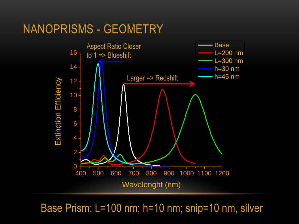
NANOPRISMS - GEOMETRY
400 500 600 700 800 900 1000 1100 12000
2
4
6
8
10
12
14
16E
xtin
ction
Eff
icie
ncy
Wavelenght (nm)
Base
L=200 nm
L=300 nm
h=30 nm
h=45 nmLarger => Redshift
Aspect Ratio Closer
to 1 => Blueshift
Base Prism: L=100 nm; h=10 nm; snip=10 nm, silver
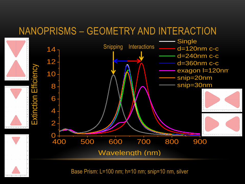
400 500 600 700 800 9000
2
4
6
8
10
12
14
Single
d=120nm c-c
d=240nm c-c
d=360nm c-c
exagon l=120nm
snip=20nm
snip=30nm
Ext
inct
ion
Effi
cien
cy
Wavelength (nm)
NANOPRISMS – GEOMETRY AND INTERACTION
Interactions Snipping
Base Prism: L=100 nm; h=10 nm; snip=10 nm, silver
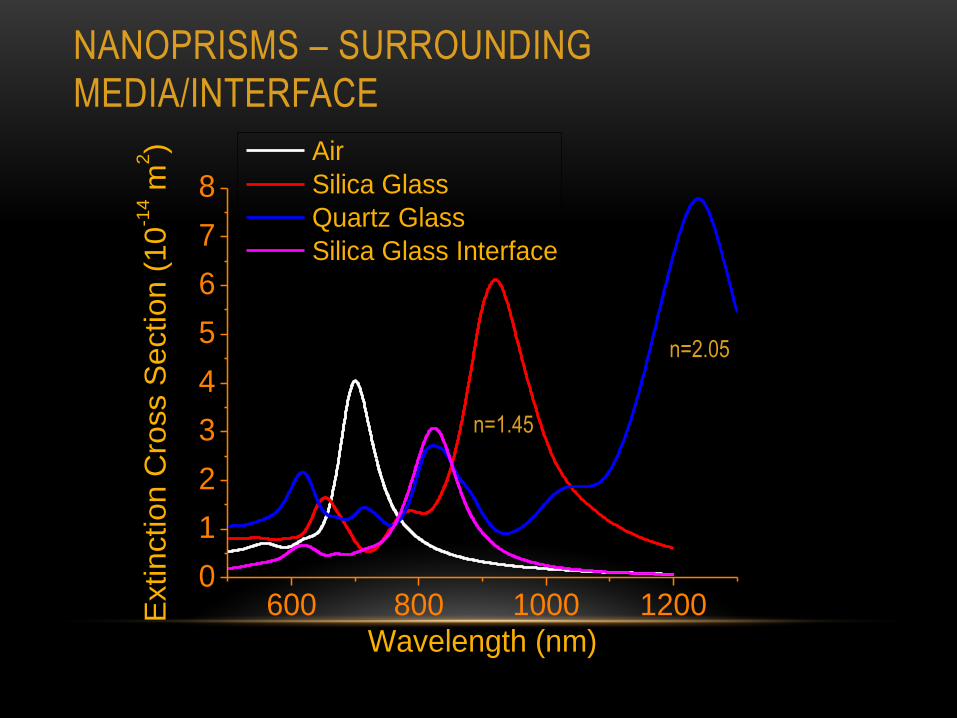
NANOPRISMS – SURROUNDING
MEDIA/INTERFACE
600 800 1000 12000
1
2
3
4
5
6
7
8E
xtin
ction
Cro
ss S
ection
(10
-14 m
2)
Wavelength (nm)
Air
Silica Glass
Quartz Glass
Silica Glass Interface
n=1.45
n=2.05
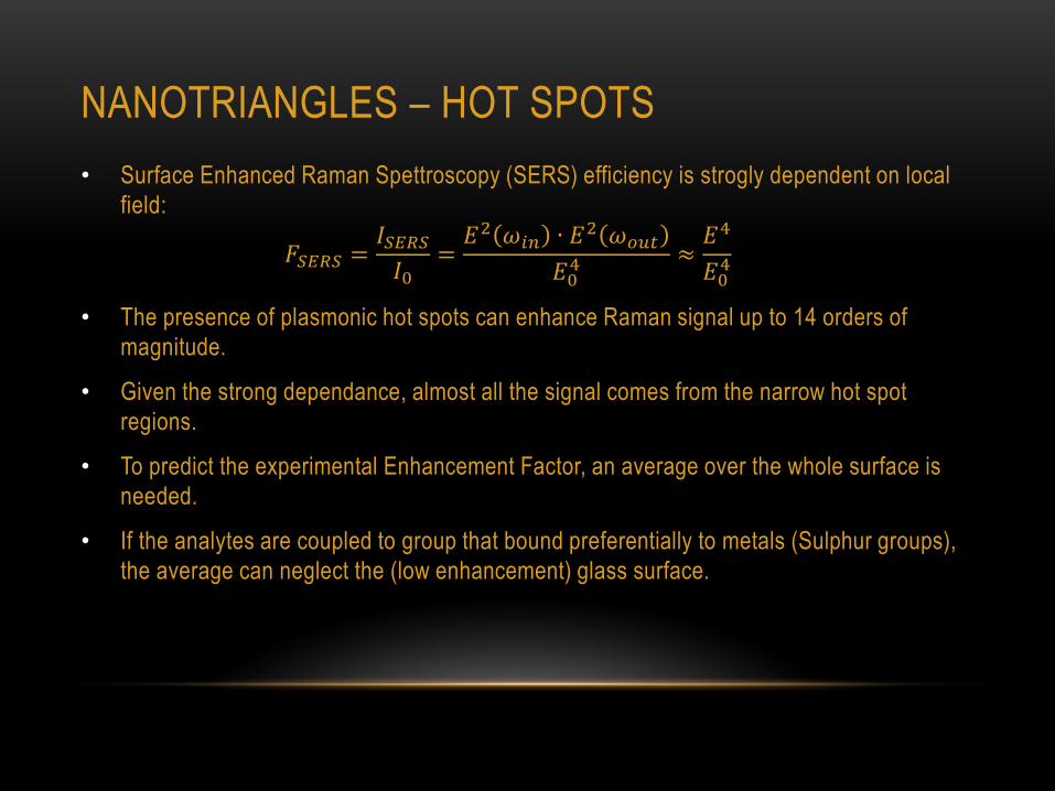
NANOTRIANGLES – HOT SPOTS
• Surface Enhanced Raman Spettroscopy (SERS) efficiency is strogly dependent on local
field:
𝐹𝑆𝐸𝑅𝑆 =𝐼𝑆𝐸𝑅𝑆
𝐼0=
𝐸2 𝜔𝑖𝑛 ∙ 𝐸2 𝜔𝑜𝑢𝑡
𝐸04 ≈
𝐸4
𝐸04
• The presence of plasmonic hot spots can enhance Raman signal up to 14 orders of
magnitude.
• Given the strong dependance, almost all the signal comes from the narrow hot spot
regions.
• To predict the experimental Enhancement Factor, an average over the whole surface is
needed.
• If the analytes are coupled to group that bound preferentially to metals (Sulphur groups),
the average can neglect the (low enhancement) glass surface.
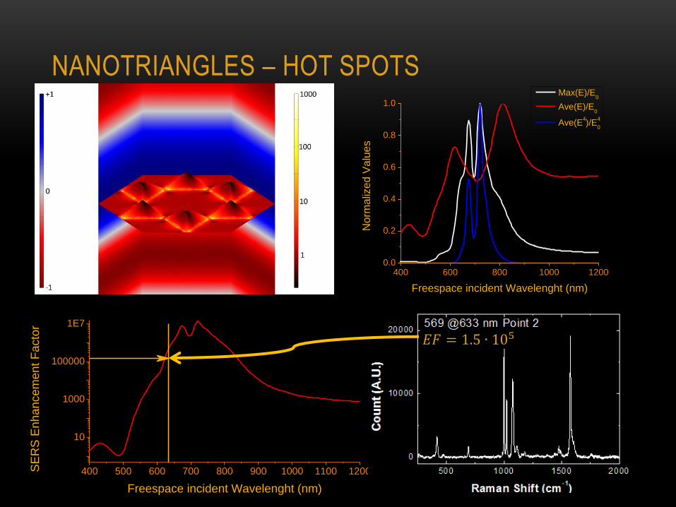
NANOTRIANGLES – HOT SPOTS
400 600 800 1000 12000.0
0.2
0.4
0.6
0.8
1.0
Norm
aliz
ed V
alu
es
Freespace incident Wavelenght (nm)
Max(E)/E0
Ave(E)/E0
Ave(E4)/E
4
0
400 500 600 700 800 900 1000 1100 1200
10
1000
100000
1E7
SE
RS
Enhan
cem
ent
Facto
r
Freespace incident Wavelenght (nm)
𝐸𝐹 = 1.5 ∙ 105
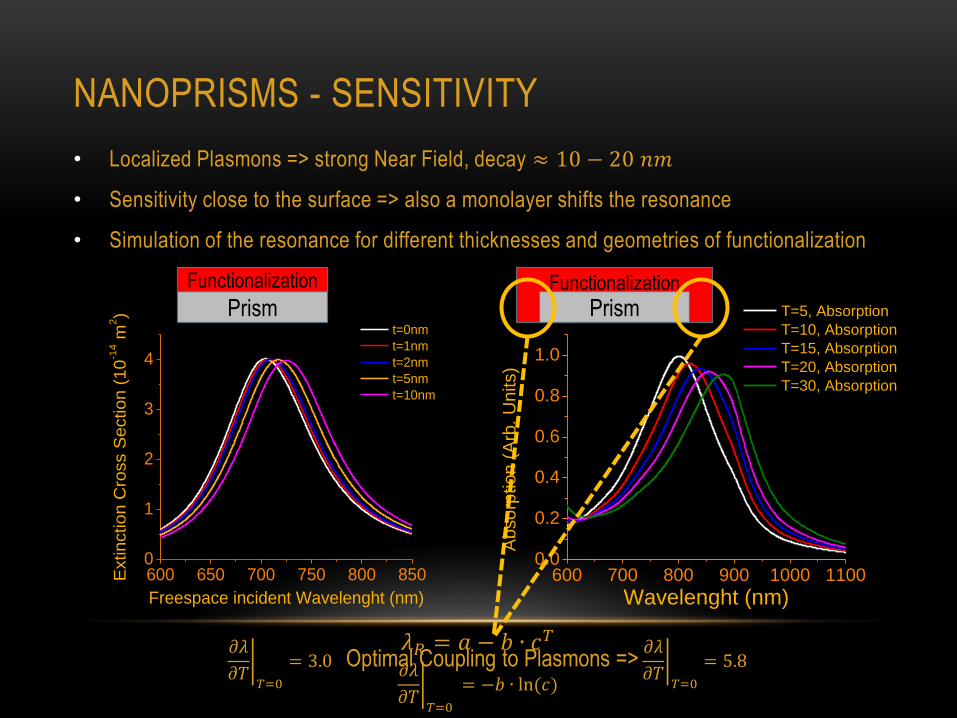
• Localized Plasmons => strong Near Field, decay ≈ 10 − 20 𝑛𝑚
• Sensitivity close to the surface => also a monolayer shifts the resonance
• Simulation of the resonance for different thicknesses and geometries of functionalization
Functionalization
NANOPRISMS - SENSITIVITY
600 650 700 750 800 8500
1
2
3
4
Extinctio
n C
ross S
ectio
n (
10
-14 m
2)
Freespace incident Wavelenght (nm)
t=0nm
t=1nm
t=2nm
t=5nm
t=10nm
600 700 800 900 1000 11000.0
0.2
0.4
0.6
0.8
1.0
Absorp
tion (
Arb
. U
nits)
Wavelenght (nm)
T=5, Absorption
T=10, Absorption
T=15, Absorption
T=20, Absorption
T=30, Absorption
Prism
Functionalization
Prism
𝜕𝜆
𝜕𝑇 𝑇=0
= 3.0 𝜕𝜆
𝜕𝑇 𝑇=0
= 5.8 Optimal Coupling to Plasmons => 𝜆𝑅 = 𝑎 − 𝑏 ∙ 𝑐𝑇 𝜕𝜆
𝜕𝑇 𝑇=0
= −𝑏 ∙ ln (𝑐)

NANOTRIANGLES - SUMMARY
• The effects of the geometric properties of the nanostructure have been investigated.
• The resonance can be taylored by tuning 4 parameters:
• Optimization tips for the two applications:
Parameters Lattice Constant Side Lenght Height Snip/Shape
Controlled by NS diameter Deposition setup Annealing
Effect of Increase Redshift Redshift Blueshift Blueshift
Reason Larger Structures AR closer to 1 Less curvature and interaction
Application SERS Refractive Index SENSING
Lattice Constant Dependent on Raman Spectrum of Analytes Dependent on the desired position of
resonance, once fixed other parameters Side Lenght Longest possible => better t-t coupling
Height Low structures => higher avg field High structures => better coupling to func.
Snip/Shape No snip, sharp edges => Hot Spots Moderate snip => more homogeneity
Tips Collimation => longer sides, sharper
edges. Evaporation => homogeneity
(no planets)
Higher Aspect Ratio, Annilation to lower
defects and strongest t-t coupling

NANOHOLE ARRAYS • Nanohole Array Parameters:
• Substrate: silica glass (n=1.445)
Computed quantities:
• Transmittance (normal, various
functionalizations)
• Reflectivity (wavelenght and angle
sweeps)
• Local fields
Parameters: Value (nm):
Lattice Constant (𝒂𝟎) (HCP) 535
Holes Radius (𝑅) 205
Film height (ℎ) 46
87
𝑎0
ℎ 2𝑅
Substrate
Functionalization Film
Holes

NANOHOLE ARRAY
REFLECTANCE – SENSITIVITY MAPS
Angle (deg)
Wav
elen
ght (
nm)
Ref
lect
ance
ℎ = 46 𝑛𝑚
𝜆 = 1140
𝜃
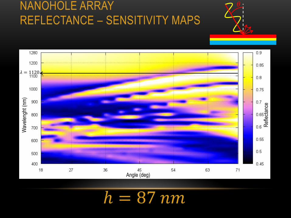
NANOHOLE ARRAY
REFLECTANCE – SENSITIVITY MAPS
Angle (deg)
Wav
elen
ght (
nm)
Ref
lect
ance
ℎ = 87 𝑛𝑚
𝜆 = 1120
𝜃

NANOHOLE ARRAY - SENSITIVITY MAPS
Reflectance – h = 46 nm
Surface: Nanohole Array on Silica (As)
Point Plot: Nanohole with Functionalization

REFLECTANCE - ℎ = 46 𝑛𝑚
45 50 55 60 65 700.55
0.60
0.65
0.70
0.75
0.80
0.85
0.90
0.95
Re
flecta
nce
Angle (deg)
T=0 nm
T=3 nm
T=4 nm
T=5 nm
T=7 nm
T=10 nm
T=15 nm
Functional-
ization T (nm)
Dip Angle
(deg)
0 57.0
3 55.7
4 55.0
5 54.3
7 53.6
10 52.3
15 50.4
𝑆𝑙𝑜𝑝𝑒 = −0.44 𝑑𝑒𝑔/𝑛𝑚

REFLECTANCE - ℎ = 87 𝑛𝑚
Functional-
ization T (nm)
Dip Angle
(deg)
0 59.1
3 58.2
4 58.0
5 57.7
7 57.0
15 54.9
45 50 55 60 65 700.60
0.65
0.70
0.75
0.80
0.85
0.90
0.95
1.00
Re
flecta
nce
Angle (deg)
T=0 nm
T=3 nm
T=4 nm
T=5 nm
T=7 nm
T=15 nm
𝑆𝑙𝑜𝑝𝑒 = −0.29 𝑑𝑒𝑔/𝑛𝑚
Experimental h = 100nm: 𝑆𝑙𝑜𝑝𝑒 = −0.18 𝑑𝑒𝑔/𝑛𝑚

400 600 800 1000 12000.0
0.2
0.4
0.6
0.8
1.0
400 600 800 1000 12000.0
0.2
0.4
0.6
0.8
1.0
400 600 800 1000 12000.0
0.2
0.4
0.6
0.8
1.0
400 600 800 1000 12000.0
0.2
0.4
0.6
0.8
1.0
400 600 800 1000 12000.0
0.2
0.4
0.6
0.8
1.0
400 600 800 1000 12000.0
0.2
0.4
0.6
0.8
1.0
400 600 800 1000 12000.0
0.2
0.4
0.6
0.8
1.0
400 600 800 1000 12000.0
0.2
0.4
0.6
0.8
1.0
400 600 800 1000 12000.0
0.2
0.4
0.6
0.8
1.0
Rhole
=200nmRhole
=150nm
Wavelenght
Transmittance
Reflectance
Absorbance
Rhole
=100nm
Nanohole Array. Lattice constant= 535 nm
Wavelenght Wavelenght
Wavelenght Wavelenght Wavelenght
Wavelenght Wavelenght Wavelenght
NANOHOLE ARRAY -
FAR FIELD AND LOCAL FIELD MAPS
Holes
T=
50
nm
T=
100
nm
T=
150
nm

650 700 750 800 850 900 950 1000
0.00
0.05
0.10
0.15
0.20
0.25
0.30
0.35
0.40
0.45
0.50
Tra
nsm
itta
nce
Wavelenght (nm)
T=0 nm
T=3 nm
T=4 nm
T=5 nm
T=7 nm
T=10 nm
T=15 nm
NANOHOLE ARRAY
TRANSMITTANCE – ℎ = 46 𝑛𝑚
640 645 650 655 6600.40
0.42
0.44
0.46
0.48
0.50
Tra
nsm
itta
nce
Wavelenght (nm)
665 670 675 680 6850.00
0.01
0.02
0.03
0.04
0.05
Tra
nsm
itta
nce
Wavelenght (nm)
860 880 900 920
0.43
0.44
0.45
0.46
0.47
Tra
nsm
itta
nce
Wavelenght (nm)

640 645 650 655 6600.40
0.42
0.44
0.46
0.48
0.50
Tra
nsm
itta
nce
Wavelenght (nm)
665 670 675 680 6850.00
0.01
0.02
0.03
0.04
0.05
Tra
nsm
itta
nce
Wavelenght (nm)
860 880 900 920
0.43
0.44
0.45
0.46
0.47
Tra
nsm
itta
nce
Wavelenght (nm)
NANOHOLE ARRAY
TRANSMITTANCE – ℎ = 46 𝑛𝑚
Thickness
(nm)
Peak 1 (nm) Dip (nm) Peak 2 (nm)
0 647.1 670.1 872.5
3 648.0 672.3 877.0
4 648.2 672.9 879.0
5 648.4 673.5 880.5
7 648.8 674.5 884.0
10 649.5 675.8 888.0
15 650.5 677.7 897.0
Feature 𝝀𝟎 (nm) Sensitivity Feature width (nm)
648 0.21 ~40
672 0.44 ~30
877 1.63 ~100

NANOHOLE ARRAY – WHICH IS THE BEST?
0 5 10 15
50
52
54
56
58
60
Slope = -0.44 deg/nm
Dip
Angle
(de
g)
Functionalization Thickness (nm)
h=46 nm
h=87 nm
Slope = -0.29 deg/nm
Transmittance, ℎ = 46 𝑛𝑚 Transmittance, ℎ = 87 𝑛𝑚
Reflectance Method Peak/dip Sensitivity (/nm)
T, ℎ = 46 𝑛𝑚 P1, 𝝀𝟎 = 647 nm 0.21 nm
T, ℎ = 46 𝑛𝑚 D1, 𝝀𝟎 = 670 nm 0.19 nm
T, ℎ = 46 𝑛𝑚 P2, 𝝀𝟎 = 872 nm 2.09 nm
T, ℎ = 87 𝑛𝑚 P1, 𝝀𝟎 = 646 nm 0.21 nm
T, ℎ = 87 𝑛𝑚 D1, 𝝀𝟎 = 666 nm 0.44 nm
T, ℎ = 87 𝑛𝑚 P2, 𝝀𝟎 = 823 nm 1.63 nm
R, ℎ = 46 𝑛𝑚 𝝀𝟎 = 1140 nm -0.44 deg
R, ℎ = 87 𝑛𝑚 𝝀𝟎 = 1120 nm -0.29 deg
0 2 4 6 8 10 12 14 16
650
660
670
870
880
890
900 Peak 1
Dip
Peak 2
Wavele
nght (n
m)
Thickness (nm)
0 2 4 6 8 10 12 14 16640
650
660
670
820
830
840
850
860
Peak 1
Dip
Peak 2
Wavele
nght (n
m)
Thickness (nm)

NANOHOLE ARRAYS - SUMMARY
• NHA can be used both in transmittance and in reflectance to build biosensors.
• SERS cannot use NHA due to low enhancement factor (~ 4-5)
• The response can be taylored by tuning 3 parameters:
Parameters Lattice Constant Hole Radius Height
Controlled by NS diameter RIE Deposition setup
Mode Transmittance Reflectance
Hole Radius Larger holes => lower absorption Smaller holes => lower dissipation
Height Thin film => higher transmittance and
better sensitivity
Thick film => lower dissipation
Thin film => better sensitivity
Tips Thin film and large holes Small holes => better conduction =>
narrower dip
Thin film => better sensitivity
• Optimization tips for the two operative modes:

CONCLUSIONS • Plasmonic Bio-Sensors design can take great advantage from nanostructures obtained by
NSL
• The design of the nanostructures can be controlled by tuning a small set of parameters, and
simulations give hints on how to obtain best performaces.
• Nanotriangles can be used both for Refractive Index-sensitive and SERS substrates. In
both cases, the agreement with experiment is pretty good, keeping in count the defects on
the real samples
• Nanohole arrays can be used both in transmittance and in reflectance
• Reflectance give the best (and most stable against defects) results
• Transmittance is far easier to measure, and it’s usable too
• Simulations show how to tune parameters to get the desired result

Thank You for your Attention!
Thanks to people, present and past members, of my group:
Boris, Carlo, Giovanni P, Giovanni P, Valentina B, Valentina M, Valentina R,
Marco, Martina
And
Tiziana and Giovanni M