Simulation & Fitting - Germanyzahner.de/pdf/SIM.pdf · 3.2.3 Phase_____ 10 3.2.4 Nyquist ... This...
88
Simulation & Fitting © Zahner 09/2013
Transcript of Simulation & Fitting - Germanyzahner.de/pdf/SIM.pdf · 3.2.3 Phase_____ 10 3.2.4 Nyquist ... This...

Simulation & Fitting
© Zahner 09/2013

SIM - 2 -

SIM - 3 -
1. Introduction ____________________________________________6
2. SIM Main Page __________________________________________7
3. Measure Data Section ____________________________________9
3.1 Load/Save Measure Data ________________________________________ 9
3.2 Specify Diagram Type of measurement data ________________________ 10
3.2.1 Impedance/phase_________________________________________ 10
3.2.2 Impedance ______________________________________________ 10
3.2.3 Phase __________________________________________________ 10
3.2.4 Nyquist _________________________________________________ 11
3.2.5 -Nyquist ________________________________________________ 11
3.2.6 1/Nyquist _______________________________________________ 11
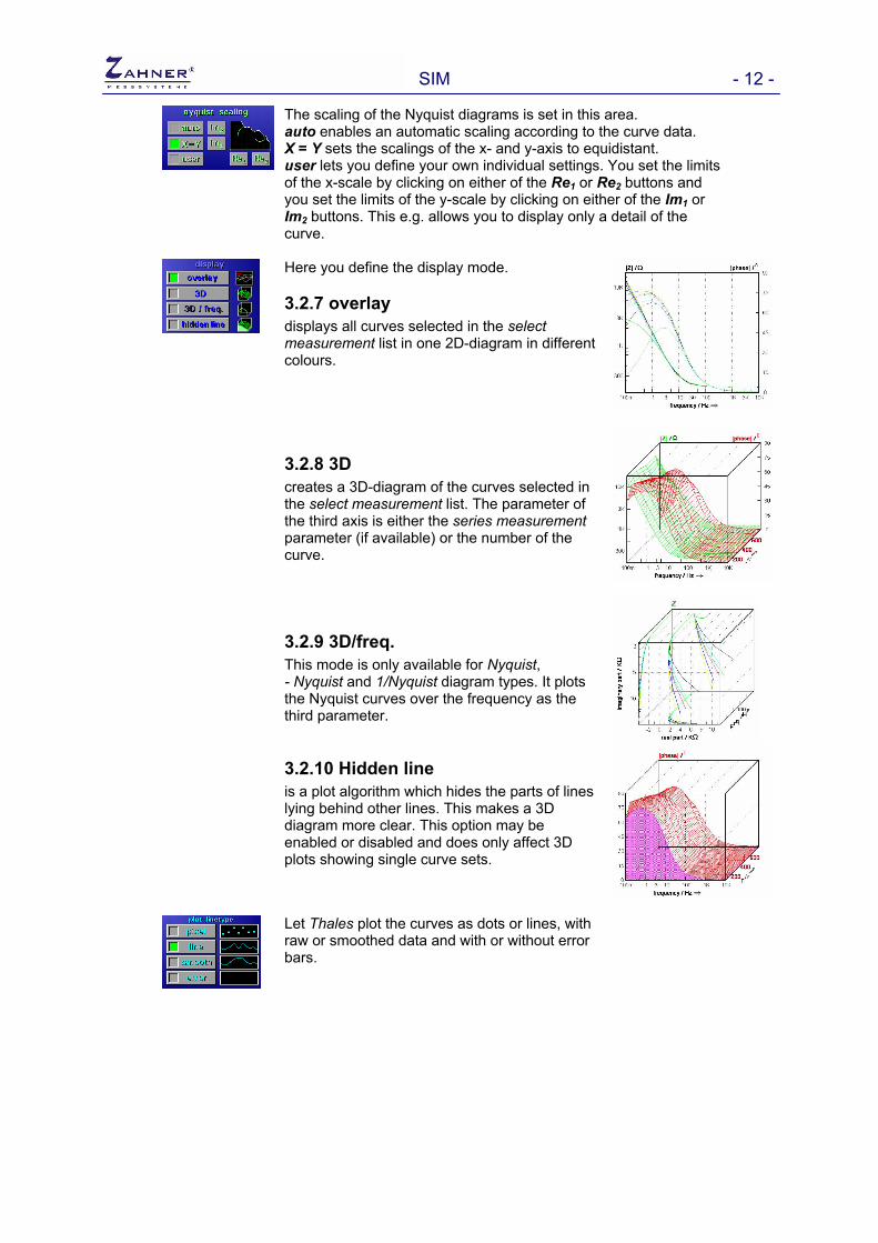
3.2.7 overlay _________________________________________________ 12
3.2.8 3D_____________________________________________________ 12
3.2.9 3D/freq._________________________________________________ 12
3.2.10 Hidden line _____________________________________________ 12
3.3 Display Diagram ______________________________________________ 13
3.3.1 Sidebar Functions ________________________________________ 13
3.4 Select Measurement ___________________________________________ 15
3.5 Z-HIT Transform ______________________________________________ 16
3.6 Kramers-Kronig Transform ______________________________________ 16
3.7 Smooth Measurement Data _____________________________________ 16
3.8 Edit Measure Data_____________________________________________ 18
3.9 Analyse Series Measure Data / Time Course Processing ______________ 18
3.9.1 Time Course Interpolation __________________________________ 19
4. Model Data Section _____________________________________21
4.1 Load/Save Model Data _________________________________________ 21
4.2 Specify Diagram Type of transfer function __________________________ 21
4.3 Display Transfer Function Diagram________________________________ 22
4.4 Select Model _________________________________________________ 22
4.5 Edit Model Circuit Diagram ______________________________________ 23
4.5.1 Impedance Elements ______________________________________ 24

SIM - 4 -
4.5.2 User Element ____________________________________________ 39
4.5.3 Element description (Help)__________________________________ 43
4.5.4 Create / Insert new element _________________________________ 43
4.5.5 Create and insert new partial scheme _________________________ 44
4.5.6 How to create a simple equivalent circuit (step by step) ___________ 44
4.5.7 How to Create a More Complicated Equivalent Circuit ____________ 47
4.6 Modifying a Model _____________________________________________ 49
4.6.1 Replace Element _________________________________________ 49
4.6.2 Insert Element ___________________________________________ 50
4.6.3 Delete Element___________________________________________ 51
4.6.4 Edit an Element’s Parameter Value Directly Including Preview ___ 51
4.7 Use of Partial Schemes_________________________________________ 52
4.7.1 Serial Connection_________________________________________ 52
4.7.2 Parallel Connection _______________________________________ 54
4.7.3 Voltage Divider___________________________________________ 54
4.7.4 Bridge Connection ________________________________________ 56
4.8 Select / New Model ____________________________________________ 56
4.9 Starting Value Finder___________________________________________ 57
4.9.1 When Entering a New Element ______________________________ 57
4.9.2 When Changing Existing Elements ___________________________ 58
4.10 Model Parameter Significance __________________________________ 59
5. CNRLS FIT ____________________________________________60
5.1 Steps to do for Fitting __________________________________________ 60
5.2 Select Samples for Fitting _______________________________________ 62
5.2.1 Manual Selection _________________________________________ 63
5.2.2 Flow Chart for a Fitting Set-up _______________________________ 64
5.2.3 How the Fitter Works ______________________________________ 65
5.2.4 Fitting Error______________________________________________ 65
5.2.5 Significance _____________________________________________ 66
5.2.6 Uncertainty (Error ∆P) _____________________________________ 66
5.3 Single Fit ____________________________________________________ 67
5.4 Series Fitting _________________________________________________ 68
5.5 Show Result of Last Fit _________________________________________ 69
6. Analyse Transfer Function Series _________________________70

SIM - 5 -
6.1 The Course of Impedance at Single Frequencies_____________________ 70
6.2 The Course of Impedance Elements_______________________________ 70
7. Modelling Transfer Functions of Photo-Electrical Systems ____73
7.1 User Elements for the Simulation of Photo-Electrical Processes _________ 74
7.2 Analyzing IMPS and IMVS Results of Dye Sensitized Solar Cells in the Traditional Way by Means of SIM ____________________________________ 83
7.3 Setting up SIM to the Joint Fitting Procedure “TRIFIT” for EIS, IMPS and IMVS Spectra ________________________________________________________ 85
8. SIM Setup_____________________________________________87
8.1 Save _______________________________________________________ 87
8.2 Recall ______________________________________________________ 87
8.3 Edit ________________________________________________________ 87
9. Init SIM _______________________________________________88

SIM - 6 -
1. Introduction This manual should be understood as a guide through the Thales simulation and fitting program. Dependent on the situation, background hints are given upon EIS analysis. A more thoroughly introduction and treatment of the ideas and theoretical basics, and how to understand the analysis strategies can be found in the manual chapter ‘Basics & Applications’. The SIM-program is a very powerful tool to describe EIS measurements by a network model consisting of elementary impedance elements (equivalent circuit). Network models can be assembled from a set of basic impedance elements, each representing impedance equivalents of physical-chemical processes. They can be connected in a specific way to built equivalent circuits, which should represent the electrical behaviour of the system under test. Besides the set of basic impedance elements, SIM networks can integrate mathematical models provided by the user in form of a formula, an algorithm or even a via DLL imported external program. As soon as a correct network description is found, a special algorithm may fit the model parameters of each element so that the transfer function of the model comes as close as possible to the course of the measured data. After a successful fit you are able to describe your measured object by a model, characterised by a specific network topology and characteristic parameters of the impedance elements present. Model-fitting can be applied to a single measurement or to a series of spectra. In the latter case the spectra of a series measurement can be fitted to a common model – a very useful function, because the resulting element parameters can be analysed and exported in dependence of the ordinal parameter of the series measurement. A unique feature of Thales is the stringent error treatment through all steps of data sampling and processing. The Zahner EIS measurement algorithm provides an uncertainty estimation for each impedance sample. This information can be used to display error-bars in the graphs of the spectra within SIM. Besides this, it is used to weight every sample point of an experimental spectrum with its individual reliability when the data are used as a basis for the fitting process. Of course, you also may create solely a model and use the software to calculate the transfer function and display the graph of it. The model data as well as the results of a fit can be saved. Furthermore, a series of spectra will be the subject of a single frequency analysis. A maximum number of 100 spectra and models can be held in memory at the same time. Thales offers different formatted numerical and graphical displays and outputs for export:
- ASCII data list - vector graphic output (Windows® EMF) - pixel graphic output (bitmap, hardcopy)
In most graphical representations a crosshair can be activated to take a closer look at the measured and fitted data. The data output may be defined in all commonly used types like BODE- and Complex Plane (NYQUIST)-diagrams. The principle proceeding of fitting EIS data to a model is as follows:
1. Load the EIS data you want to fit 2. Automatically or manually select a number of EIS data samples for the fitting 3. Create or load a model 4. Call the fitter 5. Display the graph 6. Save the model if needed
For more details please read this chapter. You will find that SIM provides a lot of very powerful functions to help you describe and understand your investigated object.

SIM - 7 -
2. SIM Main Page
Click on the icon on the Thales desktop page or click on the icon on the
EIS Main page or use the task bar navigator to open the SIM Main page: Model data section
TRIFIT Select samples for fitting Single fit Series fit
Measure data section
Load / save model data Select diagram type Display model transfer function Select model Edit model Analyse transfer function series
Load / save measured data
Define diagram
Display model data
Select data set
ZHIT test
Kramers-Kronig test
Smooth data
Edit measure data
Analyse measure series, time
interpolation
Display previous fit SIM setup Clear all data in memory
The impedance of an object usually will be measured in a defined frequency range. By analysing the resulting spectra individual impedance elements may be identified by their characteristic frequency dependence. Analysing these elements allows direct conclusions to the physical and chemical properties of the object, e.g. the thickness of a layer, the ion-concentration, the reaction-rate, the conductivity and many more. See the ‘Basics & Applications’ manual for details. Series measurements acquire impedance spectra in the same frequency range but at an altering external ordinal parameter like potential or time. In that case you obtain the course of these properties in dependence of the ordinal parameter, what opens the possibility to cancel out excessive unknowns left by the ambiguous from-principle character of transfer functions. SIM offers all the functions needed to design a equivalent circuit which is describing an impedance measurement. The user has access to all commonly used impedance elements such as resistance, capacitance, Warburg-impedance, Constant-Phase-Element, etc besides a set of advanced tools like

SIM - 8 - necessary for the modelling of porous electrodes. Moreover, by creation of user-definable impedance elements specific demands on the impedance's models may be realized using an own mathematical description. The elements can be selected and connected in different ways, supported by an easy-to-handle editor. The software calculates the transfer function of the model and the function can be fitted to the experimental data by an CNRLS fit (Complex Non-linear Regression Least-Squares fit).

SIM - 9 -
3. Measure Data Section
3.1 Load/Save Measure Data
For loading or saving data of a single or a series measurement click on this icon. You may load up to 100 data files into the memory successively. With the Select Measurement function you may select one or more files for analysing.
The following box allows you to select between: Open single measurement
Open series measurement
Save single measurement
In the following file selector box you define the path and the name(s) of the file(s) to be loaded. You may select one or more files to be loaded successively. Clicking on the LOAD button (in case of Open or Open Series) will load the file or file series. Clicking on the SAVE button (in case of Save) will save the memory-resident file to the hard disk.
During the process of loading the comment box shows the most important parameters of the measurement. Click on it to continue. The data loaded to SIM are automatically smoothed using a non-linear smoothing algorithm. This procedure prepares the data best for the fitting procedure.

SIM - 10 -
3.2 Specify Diagram Type of measurement data
Select frequency scaling type Select Nyquist scaling type Select phase scaling range Select impedance scaling type
Click on the Specify Diagram Type button to define the diagram properties you need. Select diagram type from the list: Bode (impedance & phase), Impedance, Phase, Nyquist, -Nyquist, 1/Nyquist Define display type for multiple diagram from the list: Overlay, 3D, 3D/Frequency, Hidden Line Select line type from list: Pixel (dotted line), Line, Smoothed Line, Error Symbols
Diagram type
3.2.1 Impedance/phase plots the impedance and phase data curves.
3.2.2 Impedance plots the impedance data curve.
3.2.3 Phase plots the phase data curve.

SIM - 11 - 3.2.4 Nyquist
plots the imaginary part against the real part of the impedance data (Complex Plane Nyquist diagram).
3.2.5 -Nyquist plots the negative imaginary part against the real of the impedance data.
3.2.6 1/Nyquist plots the inverse of the imaginary part against the real of the impedance data.
When active, this function references the impedance displayed as area-relative.
These parameters allow you to define the scaling of the phase axis. Pre-defined scaling are 0 – 90, -90 – 90, and -90 – 0. Selecting the user button you are able to set the scale limits according to your needs. Clicking on either of the ϕ1 or the ϕ2 button lets you enter the limits. This e.g. allows you to display only a detail of the curve.
Here you may define the scaling of the impedance axis. Normally, you will leave this on the auto setting, so that the software fits the scaling to the minimum and maximum of the impedance curve automatically. X = Y sets the scalings of the x- and y-axis to equidistant steps. user lets you define your own individual settings. You set the limits by clicking on either of the Z1 or Z2 buttons. This e.g. allows you to display only a detail of the curve.
Normally the frequency range of the Bode diagram is set automatically (auto) to the complete range of the recorded spectrum. user lets you define your own individual limits. You set the limits of the x-scale by clicking on either of the f1 or f2 buttons. This e.g. allows you to display only a detail of the curve.
SIM - 12 -
The scaling of the Nyquist diagrams is set in this area. auto enables an automatic scaling according to the curve data. X = Y sets the scalings of the x- and y-axis to equidistant. user lets you define your own individual settings. You set the limits of the x-scale by clicking on either of the Re1 or Re2 buttons and you set the limits of the y-scale by clicking on either of the Im1 or Im2 buttons. This e.g. allows you to display only a detail of the curve.
Here you define the display mode. 3.2.7 overlay displays all curves selected in the select measurement list in one 2D-diagram in different colours. 3.2.8 3D creates a 3D-diagram of the curves selected in the select measurement list. The parameter of the third axis is either the series measurement parameter (if available) or the number of the curve. 3.2.9 3D/freq. This mode is only available for Nyquist, - Nyquist and 1/Nyquist diagram types. It plots the Nyquist curves over the frequency as the third parameter. 3.2.10 Hidden line is a plot algorithm which hides the parts of lines lying behind other lines. This makes a 3D diagram more clear. This option may be enabled or disabled and does only affect 3D plots showing single curve sets.
Let Thales plot the curves as dots or lines, with raw or smoothed data and with or without error bars.
SIM - 13 -
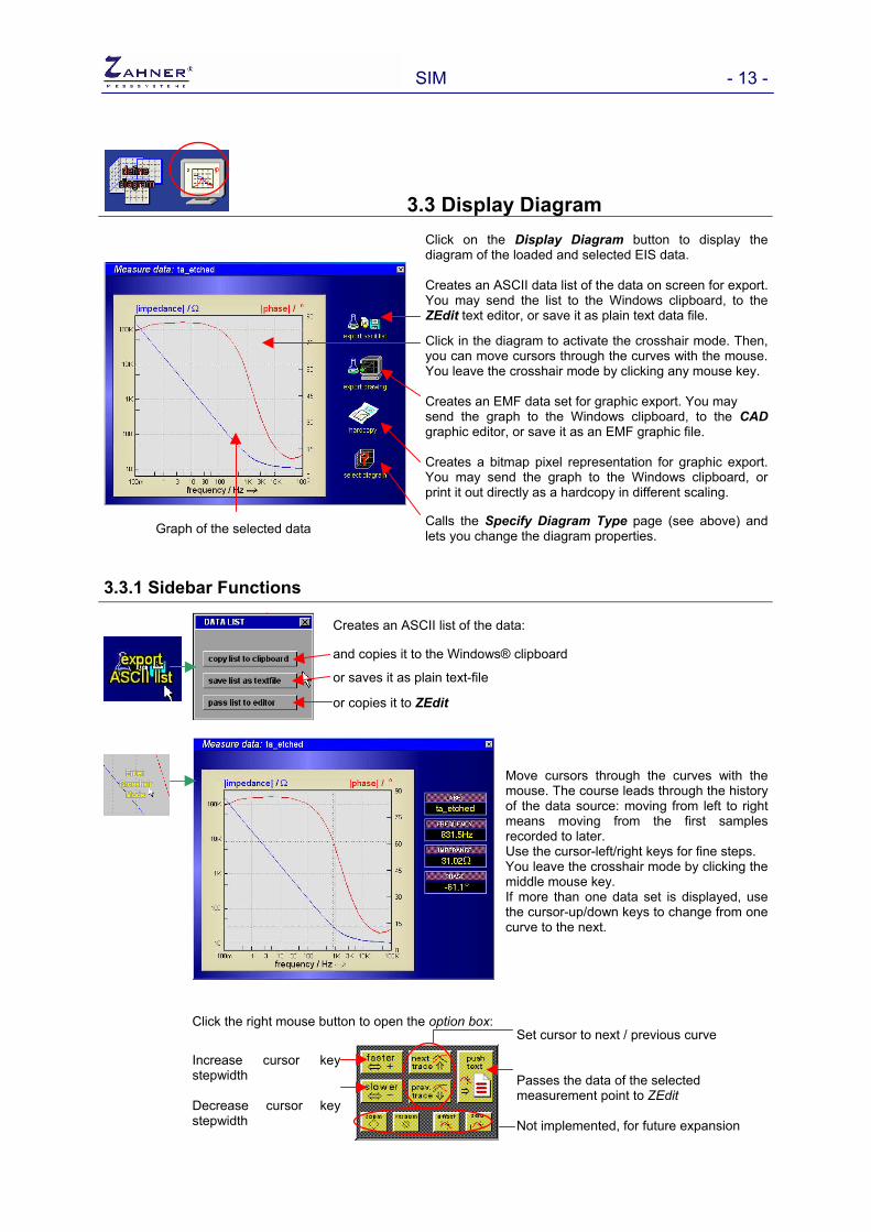
3.3 Display Diagram
Click on the Display Diagram button to display the diagram of the loaded and selected EIS data.
Graph of the selected data
Creates an ASCII data list of the data on screen for export. You may send the list to the Windows clipboard, to the ZEdit text editor, or save it as plain text data file. Click in the diagram to activate the crosshair mode. Then, you can move cursors through the curves with the mouse. You leave the crosshair mode by clicking any mouse key. Creates an EMF data set for graphic export. You may
send the graph to the Windows clipboard, to the CAD graphic editor, or save it as an EMF graphic file. Creates a bitmap pixel representation for graphic export. You may send the graph to the Windows clipboard, or print it out directly as a hardcopy in different scaling.
Calls the Specify Diagram Type page (see above) and lets you change the diagram properties.
3.3.1 Sidebar Functions
Creates an ASCII list of the data: and copies it to the Windows® clipboard
or saves it as plain text-file
or copies it to ZEdit
Click the right mouse button to open the option box:
Increase cursor key stepwidth Decrease cursor key stepwidth
Move cursors through the curves with the mouse. The course leads through the history of the data source: moving from left to right means moving from the first samples recorded to later. Use the cursor-left/right keys for fine steps. You leave the crosshair mode by clicking the middle mouse key. If more than one data set is displayed, use the cursor-up/down keys to change from one curve to the next. Set cursor to next / previous curve Passes the data of the selected measurement point to ZEdit Not implemented, for future expansion
SIM - 14 -
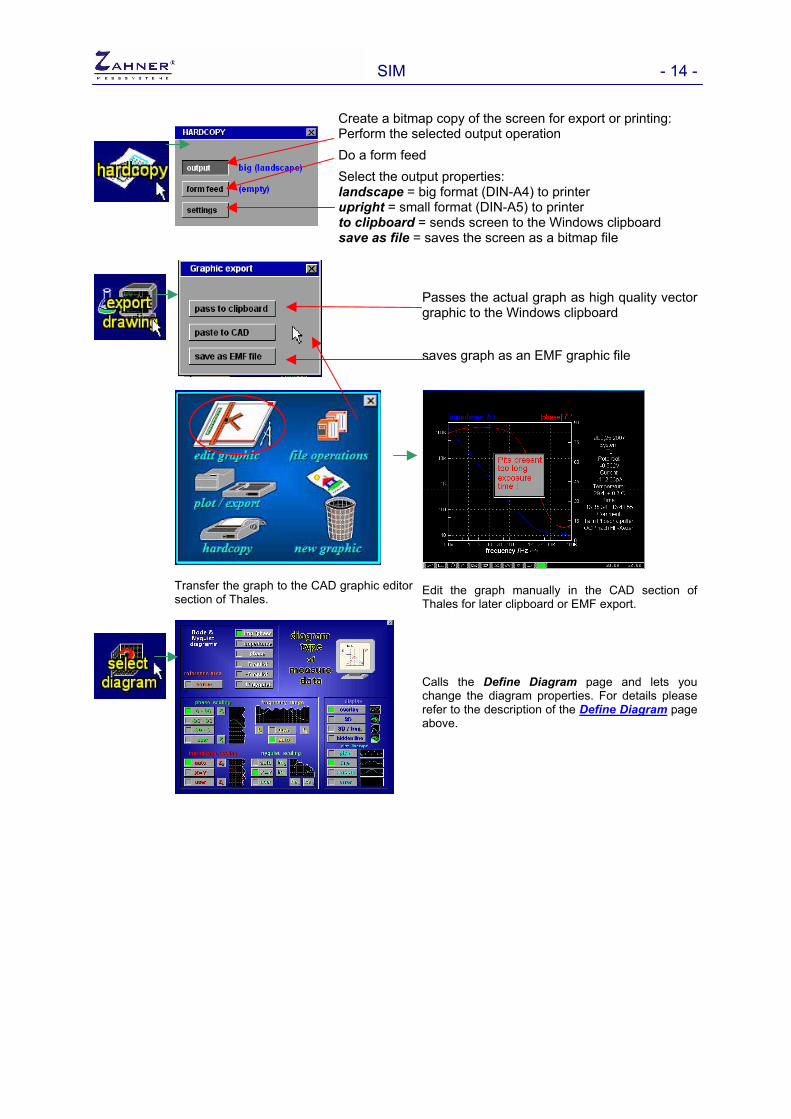
Create a bitmap copy of the screen for export or printing: Perform the selected output operation
Do a form feed
Select the output properties: landscape = big format (DIN-A4) to printer upright = small format (DIN-A5) to printer to clipboard = sends screen to the Windows clipboard save as file = saves the screen as a bitmap file
Transfer the graph to the CAD graphic editor section of Thales.
Passes the actual graph as high quality vector graphic to the Windows clipboard saves graph as an EMF graphic file
Edit the graph manually in the CAD section of Thales for later clipboard or EMF export.
Calls the Define Diagram page and lets you change the diagram properties. For details please refer to the description of the Define Diagram page above.
SIM - 15 -
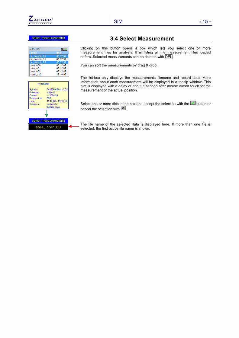
3.4 Select Measurement
Clicking on this button opens a box which lets you select one or more measurement files for analysis. It is listing all the measurement files loaded before. Selected measurements can be deleted with DEL. You can sort the measurements by drag & drop. The list-box only displays the measurements filename and record date. More information about each measurement will be displayed in a tooltip window. This hint is displayed with a delay of about 1 second after mouse cursor touch for the measurement of the actual position. Select one or more files in the box and accept the selection with the button or cancel the selection with .
The file name of the selected data is displayed here. If more than one file is selected, the first active file name is shown.

SIM - 16 -
3.5 Z-HIT Transform
The Z-HIT transform calculates the impedance data Z(f) from the Phase data ϕ(f) after the following equation.
( )ωωϕ
γωωϕπ
ωω
ω ln)(ln)(.ln
dddconstH
s
00
02⋅++≈ ∫
The result is plotted as a curve (lilac) in a graph together with the original measurement data (blue symbols) and the phase curve (red). By comparing the curve and the measurement data visually you are able to decide whether your object was in steady state during measurement or not. Furthermore Z-HIT allows you to re-create impedance data from the phase data in case a measurement was disturbed. Z-HIT is a unique function which offers a very reliable tool to judge steady state and treat steady state violations in experimental data.
3.6 Kramers-Kronig Transform
The Kramers-Kronig algorithm normally takes a little bit of time depending on the file size. Therefore a progress bar appears showing the progress of the calculation.
The Linear Kramers-Kronig transform (LKK) may be used for comparisons but is not recommended to validate the reliability of experimental data, because Z-HIT works much faster and much more reliable. Refer to: W. Ehm, R. Kaus, C. A. Schiller, W. Strunz, New Trends in Electrochemical Impedance Spectroscopy and Electrochemical Noise Analysis, ed. F. Mansfeld, F. Huet, O. R. Mattos, Electrochemical Society Inc., Pennington, NJ, 2001, vol. 2000-24, 1 for a more detailed discussion.
3.7 Smooth Measurement Data
The measurement data are smoothed automatically when loaded. In some cases the standard adjustment of the automatic smoothing is not sufficient. In that case, you may smooth the data using the algorithm with altered parameters. For this procedure the original data set is used (not the pre-smoothed ones). You can define three parameters. window width : effective width of the Gaussian shape weighing function [% of total] error weighing : switch on (1) or off (0) the error weighing

SIM - 17 -
passes : number of smoothing passes to perform The Smooth calculation of Thales uses the following algorithm:
Zsmooth (ω) = a0 + a1 * ω + a2 * ω2 + a3 * ω3 plus a Gaussian weighting:
Fweight (ω) = exp(- (ω - ω0)2 * δ) The width of the weighing function is determined by the commonly used 'half life width' of the Gaussian function. The point being smoothed is regarded as the centre of the 'Gauss' and the parameter 'width' will be given in percent of the data window's width, given in units of log(f). The new set of data will be available as well as the original ones. The 'smoothed' sample set will contain points equidistant in respect to log(f). The smoothed data set finally will be used in different operations of SIM as an alternate choice to the measured samples. It is also used for the calculation of the Z-HIT algorithm.
100m 1 10 100 1K 10K 100K
Impedance /
10%width
50
0
100
10
30
100
300
1K
3KGaussian weight /%
Frequency /
Ω
Hz
The effect of a smoothing operation will be influenced by the three parameters
- window width - error weighing - passes
The parameters can be defined in the input box appearing of the smooth function. Function Description Unit Range Default
window width The half-life width of the Gaussian weighting function discussed above
% 1 - 100 5
error weighting
Using the error weighting the smoothed data set will be calculated in a way that data points with a large error have less influence than data points with a small error.
- 0<ew<=1 0 = off
0
passes Defines the number of successive smoothing cycles applied to the data set.
- 1 - 2 1
! The execution of a smoothing operation will work on all currently selected data sets activated via the 'select measure files' function.

SIM - 18 -
Smoothing will be done automatically during loading of a measure file.
3.8 Edit Measure Data
This function allows you to edit the measurement data (impedance and phase) in a graphical way. You step through the data points with a double-cursor for impedance and phase. Moves the double-cursor over the curves. The values of the selected point (frequency, impedance, phase) are shown in the Values box to the right. The value of the selected curve (impedance or phase) is highlighted green. Switch to the phase curve Switch to the impedance curve Change the value of the selected point (data) Fix the changes you made. The changed points are marked by white squares. Press this key or the middle mouse button to exit the cursor mode.
You may save the edited set of data using the File Operations from the SIM main menu as described
above. In some cases it might happen, that an impedance measurement is disturbed at one or more measuring frequencies. E.g. due to missing shielding, power line noise of 50 or 60 Hz may be caught by an object of high impedance. SIM offers the possibility of editing single measured points and save the edited curve as an impedance file.
3.9 Analyse Series Measure Data / Time Course
Processing Series measurements Z=f(w,OP0),(OP0= const.) span up a 3-dimensional space Z=f(w,OP), OP = ordinal parameter. This space may be sliced at different frequencies within the measured frequency range. By slicing new curves will be created, the impedance and/or phase now being a function of the ordinal parameter at one selected frequency Z=f(w0,OP),(w0= const). Thus a new set of curves at different frequencies may be created being subject of further evaluations, e.g. the c/e-analysis. Output to other programs is possible by different interfaces. The single frequency analysis of measurements comes up with the menu shown below, offering different i/o-settings. Before describing the Plot Function the settings will be discussed.
Frequency Click this button to set the slice frequency Mode This button lets you chose from different graphical representations of the curve. Line: Curve is plotted as a continuous line Pixel: Data points are plotted as dots (symbols) Spline: Curve is plotted as an interpolated line Pixel/Spline: Interpolated line plus data points Click on the button repeatedly to cycle through the modes Diagram
← →
RETURN
HOME
↑ ↓
p
z

SIM - 19 -
The sliced curves will generally be plotted in the familiar BODE-representations. Click this button to select from different types: Impedance: Plots the modulus of the impedance Phase: Plots the phase angle Impedance/Phase: Plots the modulus of the impedance and the phase angle in one diagram. Click on the button repeatedly to cycle through the modes Phase Scaling The phase angle may be scaled along three different axis 0° - 90° -90° - 90° -90° - 0° Click on the button repeatedly to cycle through the modes Plot Function Click on this button to plot the data. Left to the graph you will find the already described tool icons. SIM is also able to analyse series measurement data at a fixed frequency. To do this it is necessary to load a series of EIS data files using the Load Measure Data function described above. After you selected the frequency to be analysed, a 2D-graph is created showing the ordinal parameter of the measurement series (for instance of a measurement series over time) or the number (if no common ordinal parameter is present) of the measurements on the x-axis.
3.9.1 Time Course Interpolation Series of measurements versus time can be processed in a way, that from the evolution of the impedance at each frequency vs. time a data set is reconstructed by interpolation. This interpolated data set appears “as if” no time dependence exists within a single spectrum. Each interpolated spectrum is then assigned completely to just one certain moment in time (the average measurement time of this spectrum) within the total measurement time. This procedure is very useful to eliminate excessive time drift, if one is forced to measure systems evolving in time, like following the corrosion process of a metal or the charge-discharge cycle of a battery. For a more detailed discussion how to treat time-drift affected data, refer to the ‘Basics & Applications’ chapter of the manual or read:
Validation and Evaluation of Electrochemical Impedance Spectra of Systems with States that Change with Time C. A. Schiller, F. Richter, E. Gülzow 3, N. Wagner J. Phys. Chem. Chem. Phys. 3 (2001) 374 Relaxation Impedance as a Model for the Deactivation Mechanism of Fuel Cells due to Carbon Monoxide Poisoning C. A. Schiller, F. Richter, E. Gülzow, N. Wagner J. Phys. Chem. Chem. Phys. 3 (2001) 2113 To create spectra series vs. time with each spectrum “as if measured in zero time” from drift affected data proceed as following: Use the Measure Data File Operations to open a complete measurement series which was recorded previously vs. time.

SIM - 20 -
Change the data path for spectra by means of the Measure Data File Operations to the target path for the interpolated spectra. As soon as you press time interpolation the interpolation algorithm creates a set of spectra with the same file names as the source spectra and stores them in the target directory. The target directory must not contain a file with identical name like one target name, otherwise an error message like the following will be displayed:

SIM - 21 -
4. Model Data Section
4.1 Load/Save Model Data
For loading or saving model data click on this icon. You may load one or more models into the internal memory.
The following box allows you to select between: Open a single model
Open a series of models
Save a single model
In the following file selector box you define the path and the name(s) of the file(s) to be loaded. You may select one or more files to be loaded successively. Clicking on the LOAD button (in case of Open or Open Series) will load the file or file series. Clicking on the SAVE button (in case of Save) will save the memory-resident file.
If measurement data are assigned to the model loaded, for instance due to an earlier fitting process, a comment box appears which shows the most important parameters of the measurement assigned. Click on it to continue.
4.2 Specify Diagram Type of transfer function
Select frequency scaling type Select Nyquist scaling type Select phase scaling range Select impedance scaling type
Click on the Define Diagram button to define the diagram properties you need. Select diagram type from the list: Bode (impedance & phase), Impedance, Phase, Nyquist, -Nyquist, 1/Nyquist Define display type for multiple diagram from the list: Overlay, 3D, 3D/Frequency, Hidden Line Select line type from list: Pixel (dotted line), Line, Smoothed Line, Error Enables the export of the model scheme to CAD along with the model spectrum (Create Drawing). For a detailed description of the diagram type settings refer to the chapter Specify Diagram Type of measurement data.

SIM - 22 -
4.3 Display Transfer Function Diagram
Click on the Display Diagram button to display the transfer function diagrams from the selected models.
Graph of the selected data
Creates an ASCII data list of the data on screen for export. You may send the list to the Windows clipboard, to the ZEdit text editor, or save it as plain text data file. Click in the diagram to activate the crosshair mode. Then, you can move cursors through the curves with the mouse. You leave the crosshair mode by clicking any mouse key. Creates an EMF data set for graphic export. You may
send the graph to the Windows clipboard, to the CAD graphic editor, or save it as an EMF graphic file. Creates a bitmap pixel representation for graphic export. You may send the graph to the Windows clipboard, or print it out directly as a hardcopy in different scalings.
Calls the Specify Diagram Type page (see above) and lets you change the diagram properties.
The Sidebar Functions of the Model Transfer Function page in principle are the same as for the Measure Data Section. For details please refer to that paragraph.
4.4 Select Model
Clicking on this button opens a box which lets you select one or more model files for analysis. It is listing all the model files loaded before. Selected models can be deleted with DEL. You can sort the models by drag & drop. This will be useful in order to establish the necessary order of the model sequence for TRIFIT operations. The list-box only displays the model filename and date. More information about each model will be displayed in a tooltip window. This hint is displayed with a delay of about 1 second after mouse cursor touch for the measurement of the actual position. Select one or more files in the box and accept the selection with the button or cancel the selection with .
The file name of the selected model is displayed here. If more than one file is selected, the first active file name is shown.

SIM - 23 -
4.5 Edit Model Circuit Diagram
Model name Display model parameter significance diagram
Display transfer function diagram Value list of the model circuit elements Model circuit area Model circuit diagram
List of available elements
Select element Link partial circuits Select / new model
The modelling of equivalent circuits with the Thales software is simple and straight-forward. You select one of the preset circuit elements from the list on the right hand side of the page and define its parameters and the mode of its connection (serial or parallel). The element is automatically integrated into the circuit diagram shown in the Model circuit area. In addition to the predefined elements you are able to create you own user defined elements. If you are entering a new (empty) Edit Model page you are asked to input a file name for the model to be created:
If measurement data are present, the measure file name of the top selected spectrum is proposed as model name. This box does not appear when a model is already selected in the model selector box.

SIM - 24 - 4.5.1 Impedance Elements The following table gives an overview over the impedance elements provided by SIM. The sequence follows the complexity of the data input: single parameter elements are arranged at the top. The models at the end of the list like the porous electrode model imply not only element parameter data, but are also assigned to a certain network topology.
Resistive Element RZO =
Impedance of a homogenous conductor. Same features as a resistor in electronics. The impedance is independent of the frequency. Phase angle = 0. This one-parameter element is put in straight-forward. The parameter “R” is put in as Ω. Impedance of a homogeneous conductor, e.g. the electrolytic resistance
σ⋅=Ω A
dR with d : bulk thinkness, A : cross-section, σ : specific admittance
Charge transfer resistance of faradaic impedance
*IFzTRR⋅⋅⋅
=η with −+ ⋅−−⋅= III )1(* αα , Equilibrium: 0* II =
Appearance - electrolyte resistance - Ohmic conduction - charge transfer resistance - generally resistive behaviour assigned to the hindrance of activated processes. As charge transfer resistance the Ohmic resistance is part of the total charge transfer impedance besides the diffusion- (and potentially the adsorption-) impedance component.
Capacitive Element Cj
ZC ⋅⋅=
ω1
Element with the same features as a capacitor in electronics. The higher the frequency the lower the impedance. Phase angle = -90°. This one-parameter element is put in straight-forward. The parameter C is put in as F (Farad). Electrostatic capacities, e.g. plate capacitor, double layer capacity
dAC ⋅⋅
= 0εε with ε : permittivity, A : cross-section, d : plate distance
Pseudo capacities, e.g. at adsorption
RTFzCad
Θ⋅Γ⋅⋅=
22
with Θ = mean surface concentration parameter, Γ = surface access parameter
Appearance - dielectric surface layer - double layer - adsorption impedance - crystallization impedance - generally “pseudo”-capacitive behaviour assigned to concentration dependent potential (“Nerstian capacitance”).

SIM - 25 -
Inductive Element LjZL ⋅⋅= ω
Element with the same features as a coil in electronics. The higher the frequency the higher the impedance. Phase angle = 90°. This one-parameter element is put in straight-forward. The parameter L is put in as H (Henry). Inductance of a piece of wire
rllL 00 ⋅⋅
≈µ
with µ : permeability, l : length, r : radius of wire, ml 30 10−≈
Inductance of a coil
lanL ⋅⋅⋅
=2
0 µµ with n : number of turns, a : cross-section, l : length of coil
Pseudo inductivities, e.g. one term of the relaxation impedance Appearance - wire, cable - electronic coil - “pseudo”-inductive electrochemical processes, often assigned to relaxation effects, which affect the conductivity. For the latter, refer also to the relaxation impedance.
Warburg’s Diffusion Element )1(2
jWjWZW −⋅
⋅=
⋅=
ωω
Impedance contribution W of a diffusion process as part of a charge transfer reaction. Simplest case boundary conditions assumed: one-dimensional, infinite-length diffusion. Equivalent to the “Special Warburg Impedance” after DD. McDonald. The parameter W is put in as Ω.s1/2.
R1
R = R = const C = C = consti i
R2
C1 C2
R3
C3
Rn-1
Cn-1
Rn
Cn
Transfer Function: ων
⋅⋅
⋅⋅
⋅⋅=
jDcFTR
zZ
dW
1122
2
see impedance elements expressions (31),(32),(33) for derivation and definition of terms
The upper expression is valid, if the diffusion overvoltage dominates the overall process. Otherwise the kinetic parameters of the other contributing steps may appear in the expression for ZW. Frequently a significant charge transfer overvoltage is present. This case corresponds to the “Randles equivalent circuit” (right hand figure) with the Charge transfer resistance Rct and the Double layer capacity Cdl. We then find:
Z W
C dl
R ct

SIM - 26 - Transfer Function:
with
( )jWjWZW −⋅
⋅=
⋅= 1
2 ωω
ADcFzaTRp
Wkk
kk
⋅⋅⋅⋅
⋅⋅⋅⋅=
22
ν [ ]
sW Ω
= 1
kp reaction order
kν stoichiometric number
kc concentration at x
kD constant of diffusion A surface of electrode k index of substance a Coupling factor, built from partial currents, transfer
coefficients. For details see chap. X. (at equilibrium a=1) kI partial current
xI exchange current Appearance General diffusion affected charge transfer reactions. Limiting case frequency behaviour for all diffusion contributions at high frequencies. W is a good approximation also the for lower frequency diffusion behaviour, when the maximum diffusion length given by the vessel dimensions is big compared to the range of the diffusion within a period of the test frequency. For details see also Contributions of One-Dimensional Diffusion Processes to the Impedance of an Electrode by F. Richter, Impedance Elements as part of the Thales manual.
Nernst Impedance N
N kj
jWZ ωω
⋅⋅
⋅= tanh
Impedance contribution N of a diffusion process as part of a charge transfer reaction. The boundary conditions assume a one-dimensional, finite-length diffusion limited by constant concentration. Equivalent to the “General Warburg Impedance” after DD. McDonald. The first input parameter N is put in as Ω.s1/2 like for the Warburg impedance. The second parameter k characterises the relative reach of the diffusion compared to the finite length and is put in as 1/s.
R1
R = R = const C = C = consti i
R2
C1 C2
R3
C3
Rn-1
Cn-1
Rn
Transfer Function:
ωων⋅
⋅⋅⋅
⋅⋅
⋅⋅=
jDdj
DcFTR
zZ
dN
/tanh1 2
22
2
see impedance elements expression (27.2) for derivation and definition of terms

SIM - 27 - The upper expression is valid, if the diffusion overvoltage dominates the overall process. Otherwise the kinetic parameters of the other contributing steps may appear in the expression for ZW. Frequently a significant charge transfer overvoltage is present. This case corresponds to the “Randles equivalent circuit” (previous page) with the Charge transfer resistance Rct and the Double layer capacity Cdl. We then find:
Transfer function:
with
NN k
jjWZ ωω
⋅⋅
= tanh
W = Warburg Parameter, [ ]s
W Ω= , 2
N
KN d
Dk = , [ ] 1−= skN
dN = thickness of layer, Dk = constant of diffusion
Imaginary Part /
Real Part / Ω
Ω
Diffusion length is finite due to a concentration assumed as constant in a certain distance from the electrode. The high frequency part (left part in front of the arrow symbol) of the Nyquist diagram exhibits the same shape like the the Special Warburg Impedance diagram. The low frequency part (right part behind the arrow symbol) is similar to an RC-element Nyquist diagram (semicircle). (The negative imaginary part is plotted upwards in the graph).
Appearance General diffusion affected charge transfer reactions. N is a good approximation for the frequency behaviour of the diffusion, when the free diffusion length limited for instance by convection is comparable to the range of the diffusion within a period of the test frequency (also as an approximation for a rotating disk electrode). For details see also Contributions of One-Dimensional Diffusion Processes to the Impedance of an Electrode by F. Richter, Impedance Elements as part of the Thales manual.
Finite Diffusion S
S kj
jWZ ωω
⋅⋅
⋅= coth
Impedance contribution FD of a diffusion process as part of a charge transfer reaction. The boundary conditions assume a one-dimensional, finite-length diffusion limited by blocking. Equivalent to the “General Warburg Impedance” after DD. McDonald. The first input parameter W of FD is put in as Ω.s1/2 like for the Warburg impedance. The second parameter k characterises the relative reach of the diffusion compared to the blocking distance and is put in as 1/s.
RnRn-1
Cn-1
R3
C1
R2
C1
R1
C1 Cn

SIM - 28 -
Transfer Function:
ωων⋅
⋅⋅⋅
⋅⋅
⋅⋅=
jDdj
DcFTR
zZ
dS
/coth1 2
22
2
see impedance elements expression (44.1) for derivation and definition of terms
The upper expression is valid, if the diffusion overvoltage dominates the overall process. Otherwise the kinetic parameters of the other contributing steps may appear in the expression for ZS. Frequently a significant charge transfer overvoltage is present. This case corresponds to the “Randles equivalent circuit” (previous page) with the Charge transfer resistance Rct and the Double layer capacity Cdl. We then find:
Transfer Function:
with
SS k
jjWZ ωω
⋅⋅
= coth
dydE
ADFzVW ⋅
⋅⋅⋅= , [ ]
sW Ω
= , 2S
KN d
Dk = , [ ] 1−= skN
d = thickness of layer, D = constant of diffusion, A = electrode surface
V = molar volume of bulk electrolyte, dydE
= Nernstian slope
Imaginary Part /
Real Part / Ω
Ω
Diffusion length is finite due to a phase boundary assumed in a certain distance from the electrode. The high frequency part (left part in front of the arrow symbol) of the Nyquist diagram exhibits the same shape like the the Special Warburg Impedance diagram. The low frequency part (right part behind the arrow symbol) is similar to a capacity. (The negative imaginary part is plotted upwards in the graph).
Appearance General diffusion affected charge transfer reactions. FD is a good approximation for the frequency behaviour of the diffusion, when the free diffusion length is blocked by a phase boundary (e.g. the vessel dimensions). This length is comparable to the range of the diffusion within a period of the test frequency. For details see also Contributions of One-Dimensional Diffusion Processes to the Impedance of an Electrode by F. Richter, Impedance Elements as part of the Thales manual.
Spherical Diffusion R
R kjWZ+⋅
=ω
Impedance contribution K of a diffusion process as part of a charge transfer reaction. The boundary conditions assume a three-dimensional diffusion expanding spherical from one spot into the volume. The first input

SIM - 29 - parameter W of K is put in as Ω.s1/2 like for the Warburg impedance. The second parameter k characterises the relative reach of the diffusion compared to the distance (radius of the sphere) where the concentration change due to the diffusion is assumed as negligible. It is put in as 1/s.
RR kj
WZ+⋅
=ω
with W = Warburg parameter
2rDk K
R = with KD = constant of diffusion, r = radius of sphere
Appearance Diffusion affected charge transfer reactions. K is a good model for the frequency behaviour of the diffusion for instance in micro electrodes and micro electrode arrays with low dot densities and in the case of pitting corrosion. See also About Contributions of Certain Electrode Processes to the Impedance by H. Göhr as part of the Thales manual.
Homogenous Reaction Impedance
ω⋅+=
jkWZH
*
Impedance contribution H of a diffusion process as part of a charge transfer reaction coupled with a first order chemical reaction. Also known as “Gerischer Impedance”. The boundary conditions assume a one-dimensional diffusion expanding from or into the volume. The species underlying the diffusion is generated or consumed by a homogeneous reaction in the solution. The first input parameter W of H is put in as Ω.s1/2 like for the Warburg impedance. The second parameter k characterises the relative reach of the diffusion compared to the distance where the concentration change due to the generation/consumption process is assumed as negligible. It is put in as 1/s.
ω⋅+=
jkWZH
*
)1(1122
11*
qADcFzqaTRp
W+⋅⋅⋅⋅⋅
⋅⋅⋅⋅⋅=
ν with *Icurrentexchange
Icurrentpartiala k= , A : surface of electrode
)1(0 qcpjk −⋅⋅⋅
=ν
with 0j : rate of homogeneous reaction )...( 11 ss νν →+
1
11
cc
ppq ⋅⋅⋅
=νν
Appearance Chemical reaction coupled with a diffusion affected charge transfer reaction. See also About Contributions of Certain Electrode Processes to the Impedance by H. Göhr as part of the Thales manual.
Constant Phase Element
α
ωω
ω
−
⎟⎟⎠
⎞⎜⎜⎝
⎛⋅
⋅=
00
1 jV
ZCPE
Element similar to the capacitive element, but with an absolute phase angle of less than 90°. The literature-known CPE was extended through a normalization factor ω/ω0, to enable the use of the parameter V with the dimension ‘Farad’. Setting ω0 to 1000Hz adjusts the transfer function to the impedance of a capacitor with the same ‘Farad’ value in the centre of the typical frequency range of a double layer capacity. Set ω0 to 1/2π to adjust the transfer function to the literature behaviour (see SIM setup). The parameter “V” is put in as F (Farad), the exponent α is dimensionless 1≥α. The limit value of α=1 leads to the usual capacitive behaviour.

SIM - 30 -
α
ωω
ω
−
⎟⎟⎠
⎞⎜⎜⎝
⎛⋅
⋅=
00
1 jV
ZCPE with 0ω = normalization factor
dCV δ⋅≅ [ ] FV 1= with C : layer capacity,
physical interpretation of α gradient of conductivity
dδα −= 1
=dδ
relative penetration depth
metal dielectric layer solution
d0 δ
ρ δ( )= (0)/eρ
fractal porous electrode
1
1−
=Fd
α
=Fd fractal dimension of porous surface
Metal
Solution
In practical measurement: Deviations from behaviour of an ideal capacitor
C - Ideal capacitor ω⋅
⋅=jC
ZC11
ωlog1loglog −=C
Z
slope of logZ vs. logω= -1 phase shift = -90o C: at logω=0
CPE - Loss Capacitance ( ) αω −⋅⋅= jYZCPE 0
or
α
ωω
ω
−
⎟⎟⎠
⎞⎜⎜⎝
⎛ ⋅⋅
⋅=
00
1 jV
ZCPE

SIM - 31 -
Impedance / Ω
Frequency / Hz
|Phase| 0
0
20
40
60
80
10m
1
100
10K
1 3 10 100 1K 10K 100K 1M
cap
cpe
Imaginary Part / KΩ
Real Part / KΩ
cpe
0
-30
-20
-25
-10
-15
-5
-15 -10 -5 0 5 10 15
cap
Appearance General behaviour of capacity together with Ohmic contributions in distributed systems, such as porous electrodes. Due to its nearly omnipresence, the use of CPEs should be considered carefully. CPE character is an approximate behaviour also for better characterised systems. If the origin of the CPE is known, it should be substituted by the more accurate model, like Porous Electrode or the Young-Göhr element. See also The evaluation of experimental dielectric data of barrier coatings by means of different models C. A. Schiller, W. Strunz El. Acta 46 (2001) 3619 About Contributions of Certain Electrode Processes to the Impedance by H. Göhr as part of the Thales manual.
Young’s Surface Layer Impedance
τωτω
ω ⋅⋅+⋅⋅⋅+
⋅⋅⋅
=j
ejCj
pZp
Y 11ln
1
Element describing a passive layer with conductivity penetrating from one side and decaying exponentially (by H. Göhr). It may substitute the CPE in several cases as a physical consistent model. To avoid an excess of equivocal parameters, the three characteristic parameters are normalised: p is dimensionless as the relative penetration depth of the conductivity within the dielectric. τ is the time constant of the virtual RC element built from a slice of the dielectric with its capacity and resistance at the site of the highest conductivity. The dimension is s. C is the total capacity of the layer neglecting the conductivity. It can be observed as high frequency limit capacity and is put in as Farad.
τωτω
ω ⋅⋅+⋅⋅⋅+
⋅⋅⋅
=j
ejCj
pZp
Y 11ln
1
dAC rY ⋅⋅= εε0
Capacity of the layer with cross section A and thickness d
00 =⋅⋅= xr ρεετ Time constant τ with dielectric constant ε and specific resistance ρ . At x=0 the highest conductivity will be observed
dYδρ =
Quotient of penetration depth δ of conductivity and thickness d of the passive layer

SIM - 32 -
Impedance / Ω
Frequency / Hz
|Phase| 0
0
20
40
60
80
1K
100K
10M
100µ 10m 1 100 10K 1M
p=.1
p=.05
p=.01
simulated model
τ = 100ms p = 0.1, 0.05, 0.01
C = 10µF R = 100Ω
The CPE approximation
( )qO −⋅−= 190ϕ Phase shift ϕ of the Young Göhr Impedance with
( )p
tq 1ln
1
+⋅=
ω
1. Strong gradient in conductivity d<<δ ⇒ relative penetration depth 1<<p
2. High frequencies ( )p
t 1ln <<⋅ω
⇒ q constant
-3 -2 -1 0 1 2 3 4 50
15
30
45
60
75
90
90° * 1- [ ln(ω*10-5 )+32] -1 90° * 1- [ ln(ω*10-4 )+16] -1
90° * 1- [ ln(ω*10-5 )+16] -1 - pha
se a
ngle
[ °
]
log frequency [Hz]

SIM - 33 - Appearance Oxide layers on metal electrodes like Fe, Al, Ti, Ta …, organic coatings under soaking effects. See also Impedance Studies of Layers with a Vertical Decay of Conductivity or Permittivity U. Rammelt, C.-A. Schiller Acta Chim. Hung. 137 (2000) 199 The following impedance models do not only characterise their own parameter set, but imply also a certain topology of the network. For instance, the Relaxation Impedance applies to the changes of the behaviour of a general charge transfer reaction (CTR) under certain conditions. The impedance elements describing the CTR are indispensable when applying the relaxation impedance. A similar situation is present when applying the Porous Electrode model: The input of the porous electrode model parameters, like the electrolyte conductivity in the pores, only makes sense together with the description of the affected electrode surface. The sequence to establish these models is more complicated than the input of the concentrated elements described before. Therefore the way how to set up these models is described individually in the following. For that we have to use some information, in particular the ‘Creation and Insertion of Partial Schemes’ which is described later in the manual.
Relaxation Impedance
k
CF
ZR
ZZRZ
η
θη
+
++=
1
The RI element describes a Faraday Impedance at a non-equilibrium potential (by H. Göhr). The charge transfer reaction rate is assumed as potential-dependent, undergoing a relaxation with time. Assumptions: - the system shall be apart from equilibrium - the rate constant k is assumed as potential dependent - the settling of k is assumed as delayed with a time constant τ The ratio between active and passive surface areas determines the effective reaction rate. The delayed settling of that ratio to a new equilibrium state after a potential change will often cause the ‘relaxation impedance’.
electrode surface
passivearea
activeareas
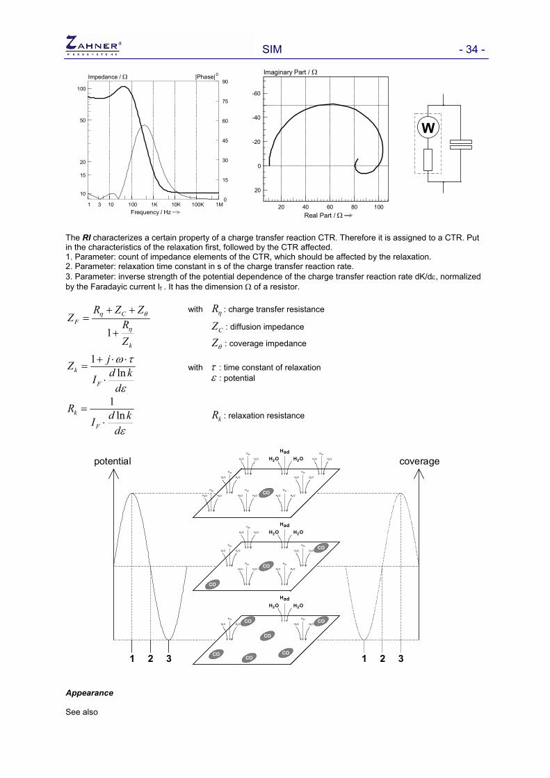
SIM - 34 -
Impedance / Ω
Frequency / Hz
|Phase|0
0
15
30
45
60
75
90
10
20
15
50
100
1 3 10 100 1K 10K 100K 1M
Imaginary Part / Ω
Real Part / Ω20 40 60 80 100
0
-60
-40
-20
20
W
The RI characterizes a certain property of a charge transfer reaction CTR. Therefore it is assigned to a CTR. Put in the characteristics of the relaxation first, followed by the CTR affected. 1. Parameter: count of impedance elements of the CTR, which should be affected by the relaxation. 2. Parameter: relaxation time constant in s of the charge transfer reaction rate. 3. Parameter: inverse strength of the potential dependence of the charge transfer reaction rate dK/dε, normalized by the Faradayic current If . It has the dimension Ω of a resistor.
k
CF
ZR
ZZRZ
η
θη
+
++=
1
with ηR : charge transfer resistance
CZ : diffusion impedance
θZ : coverage impedance
ε
τω
dkdI
jZF
k ln1
⋅
⋅⋅+= with τ : time constant of relaxation
ε : potential
εdkdI
RF
k ln1
⋅=
kR : relaxation resistance
CO
H 2H O2O
adH
H 2H O2O
adH
H 2H O2O
adH
H 2H O2O
adH
H 2H O2O
adH
H 2H O2O
adH
H 2H O2O
adH
H O2H O2
Had
H 2H O2O
adH
H 2H O2O
adH
H O2H O2
Had
CO
H 2H O2O
adH
H 2H O2O
adH
H 2H O2O
adH
H 2H O2O
adH
H 2H O2O
adH
H O2H O2
Had
CO
CO
CO
CO
COCO
CO
CO
potential
1 32 1 32
coverage
Appearance See also

SIM - 35 - Relaxationsimpedanz als Verknüpfung von Impedanzelementen H. Göhr, C. A. Schiller; Z. Phys. Chem. Neue Folge 148 (1986) 105 Relaxation Impedance as a Model for the Deactivation Mechanism of Fuel Cells due to Carbon Monoxide Poisoning C. A. Schiller, F. Richter, E. Gülzow, N. Wagner J. Phys. Chem. Chem. Phys. 3 (2001) 2113 Example Here is an example for the input sequence of the relaxation impedance. Let us start with the set-up of the relaxation parameters: we assume that the CTR affected should contain two components: the CT resistance and a certain diffusion model.
So we have to set the “count N” to two. Then we chose the relaxation time constant to 1 ms. This corresponds to a transition frequency of around 1 KHz. At significant higher frequencies the RI behaves no longer approximately like a R/CPE, but more like a proper capacity. The third parameter value Rk can be understood also as a change of the CT resistance under the influence of relaxation. When we extract (from the experimental data) a change of the 1 KΩ CT resistance observed in the range of 10%, we set Rk to 100Ω. Now the RI is complete. We confirm and at the screen an empty dotted frame appears:
It is a place holder for the latter completion with the two elements which must describe the CTR impedance. Now let us continue with the input of the CT resistance and a Warburg element in series in the conventional way to complete the RI . It looks then like:
To complete the circuit into a modified Randles circuit we finally have to add the double layer capacity in parallel and the electrolyte resistance in series:

SIM - 36 -
Porous Electrode )()1(
)(2)1(
00
022
*|| qqCqqS
qsqpSspCCZZZnn
nS +⋅+⋅+⋅
⋅+⋅⋅+⋅⋅⋅−+⋅+=
Impedance simulation of a system of homogenous pores (by H. Göhr). The complexity of the Porous Electrode element PE depends on the application. Generally the PE working principle is as follows: the impedance components of a porous system, for instance its electro-active surface q within the pores, is first put in conventionally “as if” belonging to a smooth, undistributed system. You can define the electro-active surface model without functional restrictions, but consider, that the meaning of some parameters may change when the impedance element is used within a pore. If you use the PE in its more complex form, you may consider other characteristic partial impedance besides the electro-active surface q, in particular the pore ground impedance n and the top layer impedance o. In this case you have to define o and n as uncommitted partial impedances first. Next is the description of the electro-active surface q in form of a partial impedance. Finally put in the PE code number and the PE characteristic parameters integral pore electrolyte resistance p[Ω] and integral solid resistance s[Ω] and connect it in series to q. Note, that this will complete the circuit, although the circuit builder still indicates open partial schemes!
SZ impedance of the porous layer
pZ impedance of the pores containing electrolyte
qZ Impedance of the interface porous layer / pore
oZ impedance of the interface porous layer / electrolyte
II
Zo Z∆ s Z∆ s
Zp∆ ZnZp∆
Zq∆
Zq∆
Zq∆
Zq∆
nZ impedance of the interface porous layer / bulk
SZ
LAYER
qZ
ZnPZ
ZO
PORES
)()1()(2)1(
00
022
*|| qqCqqS
qsqpSspCCZZZnn
nS +⋅+⋅+⋅
⋅+⋅⋅+⋅⋅⋅−+⋅+=
qsp ZZZZ ⋅+= )(* , sp
sp
ZZZZ
Z+
⋅= , )cosh( *Z
ZZC sp += , )sinh( *Z
ZZS sp +=
sp
p
ZZZ
p+
= , pZZ
Zs
sp
s −=+
= 1 , 0
*
0 ZZq = ,
nn Z
Zq*
=
H.Göhr et al., Kinetic Properties of Smooth and Porous Lead / Lead Sulfate Electrodes 34th I.S.E. Meeting, Ext. Abstracts, Erlangen, (1983) This early model is based on the assumption of uniform pores following Cavalieri’s principle. It was shown later by L. Bay & Key West, Solar Energy materials and Solar Cells 87 (2005) 613-628, that this model is also appropriate, if electronic and ionic conductivity in matter is distributed over space, building current paths in form of a ladder network (ZO and Zn must then be omitted). An application is shown on the next page.

SIM - 37 - Göhr´s Porous Electrode Impedance, Applied as Differential Ladder Network to the SOFC Cathode
current collector
yttrium stabilized zirconia
electronicconductor
ionicconductor
electronicpath
ionic path
e-e-e-
O2- O2- O2-
current collector
contact
electronic conductor ionic conductor
contact
electrolyte
metal
outerpore surface
infinite
infinitee-O2-
Reaction: O2 + 4 e- -- 2 O( Z q = impedance of reaction sites )
-inner pore surface
- fluxe through
outer pore surface- fluxO2- through
> 2-
O - flux PZPZ2-
qZqZ
-- fluxSZSZ e
Appearance Batteries, fuel cells, surface layer of corroding electrodes, non-homogeneous oxide layers. Example Let us built up PE circuits of different complexity in ascending order.
Let us start with the definition of a Randle circuit, where we stop without adding a (concentrated) electrolyte resistance. The description look like this:

SIM - 38 -
Then we yield:
If we omit the diffusion impedance #2 in the Randle circuit, we will find the porous electrode properties of the model after De Levie (a chain latter behaviour). At this state we could add a concentrated electrolyte resistance to the circuit in series to complete our description. Instead let us now built up the most complex form of the PE impedance, which includes both top surface- as well as pore ground impedance o and n. In this case we have to put in first the top surface impedance o as a partial scheme (13Ω), next the pore ground impedance n (16Ω) as a second partial scheme (we use resistors, but there is no restriction in complexity). Then we built up the q-interface for the electro-active pore area in a third partial scheme (here without diffusion impedance). Then we put in the PE characteristics, now with a code number of four, and complete the circuit by putting the PE in series to q.
Universal Impedance Matrix (unimplemented)
Diffusion Impedance (unimplemented)
For future extension
For a additional background information please refer to the manual chapter ‘Basics & Applications’ and ‘Impedance Elements’.
Note, that the PE symbol is introduced as adizzy shading at the top connection line of the qimpedance. Please recognize, that we put in thebulk resistance as zero, assuming it is negligibledue to a metallic character of the bulk comparedto the electrolyte. At least one of bothresistances must be different from zero.
Next we add the PE model tocomplete the description ofthe electrode:

SIM - 39 -
4.5.2 User Element General The User Defined Element (UDE) enables you to define transfer functions fitting your special needing, if you cannot find the appropriate impedance element in the SIM library. A UDE is relatively simple to create by means of an ASCII text based description, written in “andibasic”. andibasic is an easy to use programming language, which supports all mathematical functions necessary to describe transfer functions in an elegant way. Impedance elements are defining a complex function
Impedance = f(Par1,Par2,...,Parn,T). Due to the mathematical algorithm, defined by the user, the complex impedance will be calculated as a function of the reciprocal angular frequency, transferred to the UDE function by means of the common variable T
fTfT
⋅==
11ω
with the constant π⋅
=2
1Tf
and up to 16 describing parameters
Par1 (,Par2,...,Par16 ) After a user element is defined it can be taken in the same way as any other preset impedance element of the library. The possibility of saving user defined elements offers the ability to create an individual library of an infinite number of UDEs, where up to five different UDEs may be present in a model (however, consider that the maximum count of model parameters is 64 !).
!
A limited syntax and logical check is applied during the compilation. In case of mathematical or logical errors in the description a runtime error may occur. E.g. defining a statement a=1/b with b=0 will cause a 'division by zero error' during execution.
!
Redefining a user element may lead to conflicts with the structure of an actual model present. If different models will be loaded containing user elements, make sure that the same definition and only up to five elements will be used. Before loading a model containing a user element make sure that the compatible UDE is present.

SIM - 40 - Creating an user element For defining a user element you use the Thales editor ZEdit. Please note that the definition requires some rules of structure and format. The following box shows the coarse structure of a user element. In the definition block of the parameter(s), the string constants needed in the parameter input box and the mathematical definition block are defined.
Definition Definition
line 1 line 2
n TITLE(ger), title(eng)
Parameter : Parameter
line 1 : line n
MAGN1(ger), magn1(eng), min1, max1 : MAGNn(ger), magnn(eng), minn, maxn
Formula start Formula Formula : Formula Formula end
line 1 line 2 line 3 : line m-1 line m
formula: local IN1,IN2,...,INn-1,INn math. expression math. expression : math. expression fnend Result&
As you can see, three main blocks have to be defined: The Definition block with header information, the Parameter block with the string constants needed for the input boxes and the Formula block containing the mathematical description of the user element. Definition block Line 1: indicates the number n of parameters being defined in the Parameter block.
NOTE: A maximum number of 16 parameters are accepted.
Line 2: defines the headline string of the I/O-boxes. NOTE: Due to the internal structure both, German and English, titles have to be defined. They have to be separated by a comma. Two successive commas mean that the corresponding string is kept empty.
Parameter block In the Parameter block you define the number of string parameters (n) you announced in the Definition block. Each line contains the following parameters separated by a comma:
1. A string literal describing the input quantity in German. 2. A string literal describing the input quantity in English. 3. The lower limit (minimum) of the parameter range. 4. The upper limit (maximum) of the parameter range.
Parameter 3. and 4. will check the range of each parameter during input and fitting at runtime. Range violations are indicated by a less! or more! message and must be corrected by a new input at runtime. They are also respected by the fitter as limit values. The quantity string must contain both, text and unit of the parameter separated by a slash “/”. Example: Druck/bar,pressure/bar,1e-3,10 defines a parameter with the quantity “pressure” in units of “bar” in the range of “1 mbar” to “10 bar”. Formula block In the formula block the mathematical definition of the complex Z&-function is set. As mentioned above some rules regarding format and structure have to be noted. Special keywords must be input without spaces and in lower case letters. Line 1: The first line of the Formula block must read:
formula: local

SIM - 41 -
followed by the list of the parameter names in the order they were defined before in the Parameter block, separated by a comma. the 1st variable name stands for the 1st free parameter the 2nd variable name stands for the 2nd free parameter : the nth variable name stands for the nth free parameter. Following the last variable of the list you may define some more variables you are using within the mathematical description, e.g. for storing intermediate results. Variable names will contain implicit type definitions as trailers behind the ASCII text names as follows: Real type : no indicator Integer type : %-Indicator Complex type : &-Indicator Examples: Real, Integer%, Complex& NOTE: All keywords have to be written in lower case letters. For variable names use CAPITAL letters (at least for the first character) to avoid erroneous keyword translations. The local definition is necessary to declare the used variables as local types, avoiding the erroneous use of variables reserved by SIM. IMPORTANT: The common variable T is reserved for the transfer of the calculating frequency into the formula, it contains the inverse angular frequency (see examples).
The common constant Tf with π⋅
=2
1Tf , may be used for typical conversion
operations. Do not use it with a different meaning. Line 2: The mathematical definition block will contain all statements Line m-1: to calculate the returned function value. Line m: At the end of the formula evaluation there must be a complex value for the impedance
to be retransferred via the fnend statement to the SIM caller. NOTE: All statements must be separated by colons or located in different lines, spaces may be omitted, no spaces are allowed within names and keywords, comments may follow after ' at the end of the line or after the keyword rem. Examples of user elements Example 1 (a principle demonstration without physical meaning) 3 '3 parameters' Testelement, test element 'Deutscher Titel, English title' Seltsamkeit/S0,strangeness/S0,-1,1 'Parameter 1 ---> Strangeness' Charme/C1,charme/C1,-2,2 'parameter 2 ---> Charme' Farbe/f,color/f,1,3 'parameter 3 ---> Color' formula:local Strangeness,Charme,Color,Dummy,Z&,Real,Imag Dummy=10 Real=T*Strangeness Imag=Charme^Color Imag=Imag/T-Charme Z&=cmplx(Real,Imag) Z&=Dummy*Z& fnend Z&

SIM - 42 - Example 2 (a special diffusion impedance for SOFC) 4 Landeselement1,Landes element1 O2-PDruck/p,x0/p,0,1 Auststromd./Acm-2,Id/Acm-2,1e-6,1e3 Stromdichte/Acm-2,I /Acm-2,1e-6,1e3 Omega0/Hz,Omega0/Hz,1e-3,1e6 formula: local x0,Id,I,Omega0
local Beta,Gamma,Eplus&,Eminus&,Tau&,Tp&,Tm&,Z0,Z& Gamma=1/T/Omega0:Beta=I/Id Tau&=csqr(cmplx(1,Gamma/Beta^2)) Eplus&=cexp(Beta*Tau&/2):Eminus&=1/Eplus& Tp&=1+Tau&:Tm&=1-Tau& Z0=2.63e-2*(1-x0)*exp(Beta)/(1-(1-x0)*exp(Beta))/Id Z&=cmplx(0,1)*2*Beta/Gamma Z&=Z&*(Tp&^2*Eminus&-Tm&^2*Eplus&-4*Tau&*exp(-Beta/2)) Z&=Z&/(Tp&*Eminus&-Tm&*Eplus&)
fnend Z0*Z& Usage and Definition of an User Defined Element from SIM Entering the UDE menu by pressing the
aa
button of the Define Elements page will open the selector box, which displays the already defined UDEs together with the option fields for UDE definition.
Choosing one of the first five selections willenter one of the already defined UDEs. In theexample displayed, UDEs for a photo-electriccurrent source, different special boundarycondition diffusion elements and a porouselectrode description after De Levie are alreadydefined. Selection of for instance the thirdUDE, the ‘Landes Element1’ from the aboveexample 2 will open the following input field:
When you confirm the input box, the circuit diagram willdisplay the set of parameters assigned to the UDE togetherwith a UDE-symbol. The symbol carries the number of theUDE as identification label. The pre-defined UDE is nowintegrated in the actual equivalent circuit model.
Choosing one of the selections labelled with ‘Redefine element #’ will start thenew(re)-definition of the selected UDE. SIM assumes that the mathematicaldescription is present in the working space of ZEdit as an ASCII text and willtry to compile it. After a successful compilation, SIM will display the message:
The UDE will be stored permanentlyin SIM for future use.

SIM - 43 - From now on the just defined element may be used as any other standard element of the library. Do not forget to save the correct source text-file definition from ZEdit, this is not automatically performed!.
4.5.3 Element description (Help) Right-clicking on an Impedance Element opens this online manual explaining the element and giving the transfer function formula.
right-click
4.5.4 Create / Insert new element To insert a new element click on one element in the Impedance Elements list. Input a starting value for this element in the input box to follow:
Now you have to select the type of connection of the new element to the existing elements. If it is the first element to be set, select the button New Partial Scheme. Create a new partial scheme (stack the previous scheme) or set the first element Serial connection of the actual element to the open partial scheme Insert the new element at the actually reached point of the scheme Arrange the new partial scheme together with one previous scheme on stack as a voltage divider
close no. of the next element Parallel connection of the actual element to the open partial scheme Delete the actual element Arrange the new partial scheme together with four further partial schemes on stack as a bridge connection

SIM - 44 -
4.5.5 Create and insert new partial scheme A model circuit in general consists of one or more partial circuits which can be connected in parallel and in series. Each partial circuit consists of one or more impedance elements. The input and the arrangement of a circuit always are done in a linear way: The partial circuit or the impedance element to add will be connected to the already existing circuit or element. These elements will be connected in parallel or in series, depending on the indicated type of circuit.
4.5.6 How to create a simple equivalent circuit (step by step) To get familiar with the model's editor let’s do an easy example with only one partial scheme. We assume an ideally polarizable electrode, consisting of an ideal capacitor C, describing the double-layer capacity, and a resistor R, describing the electrolyte resistance.
If you have worked in the model editor before use the 'INIT'-button in the SIM menu to reset the program to its initial state.
Call the model editor by Create/Edit Model in the SIM menu.
Name the model for instance “electrode”.
Move the mouse to the Resistor symbol.
To get some information about the physical and chemical meaning of that element, use the help function (right mouse button). Within the help window the relevant parameter(s) of the selected element will be marked by red rectangles.
Left-click on the Resistor symbol to select this element and enter 100 (for 100 Ohm) in the input box and confirm with the key. RETURN

SIM - 45 -
As the resistor is the first element of a new model (and therefore also of a new partial scheme) select
in this window.
The selection of the first element is finished now and the element R/100Ohm appears in the model-circuit window. To append further elements the editor prompts with
After the resistor has been defined a capacitor must be appended by a serial connection to complete the circuit scheme of our example.
Move the mouse to the capacitance symbol and left-click to select it.
Enter the value of 1 microfarad by typing “1u”. Generally, besides the usual writing conventions for numbers like ‘1e-6’ or ‘0.000001’, parameter values are accepted in engineers units by Thales for convenience: a = atto = 10-18
f = femto = 10-15
p = piko = 10-12
n = nano = 10-9
u = micro = 10-6
m = milli = 10-3
K (or k) = kilo = 103
M = mega = 106
G = giga = 109
T = tera = 1012 P = peta = 1015 E = exa = 1018 (Capital ‘E’ !. Do not mix with exponential style ‘e’ !)
The capacitor shall be connected to the resistor by a serial connection. Thus select the option 'serial connection'

SIM - 46 -
In the model-circuit-window we will see now our completed model of an 'ideal polarizable electrode', the circuit being represented by common technical symbols and the elements' values being printed in a separate list at the top of the window. The new model is now available under the name “electrode”. Do not forget to save the model as file using the Model File Operations in the SIM menu if you want to use it later on.

SIM - 47 -
4.5.7 How to Create a More Complicated Equivalent Circuit The Randles circuit (the linear way)
If you have worked in the model editor before use the 'INIT'-button in the SIM menu to reset the program to its initial state.
Call the model editor by Create/Edit Model in the SIM menu.
Name the model for instance “Randal_1”.
Select the Resistor element and enter 100k (for 100 kΩ). This element shall represent the charge transfer resistance.
Select New Partial Scheme to begin the new schematic.
Select the Warburg Diffusion Element and enter the value of “50” for 50 Ω/s½. It represents the diffusion impedance which completes the Faradayic impedance in a Randles circuit.
The Warburg Diffusion Element has to be connected in series to the resistor. Thus select Serial Connection.
Select the Capacitive Element and enter “10u” for 10 µFarad. This element represents the double layer capacitance.
As the capacitor must be parallel to the existing partial schematic select Parallel Connection.
Now we have to add a resistor representing the electrolyte resistance. Enter “100” for 100 Ω.
As the resistor must be put in series with the existing partial schematic select Serial Connection.

SIM - 48 -
The model should look like this, now.
The Randels Circuit (Using partial schemes)
Click on the Select/New Model button to create a new model. Enter the name of the model to create “Randal_2”. Click on the Clear button to begin with an empty page.
Name the model “Randel_1”.
Select the Capacitor symbol (double layer capacitance) and enter “10u” for 10 µFarad.
Select New Partial Scheme.
Select the Resistor element (charge transfer resistance) and enter “100” for 100 Ω
Select New Partial Scheme in order to create a second branch of the schematic.
Select the Warburg Diffusion Element and enter a diffsion of “50” for 50 Ω/s.
Select Serial Connection to connect the Warburg Element in series to the resistor (active branch).
Now click on Connect Partial Schemes and on Parallel Connection to connect the two branches in a parallel way.

SIM - 49 -
Now we have to add a resistor representing the electrolyte resistance. Enter “100” for 100 Ω.
As the resistor must be in series to the existing partial schematic select Serial Connection.
The model should look like displayed left now. Please recognize, that the physical properties of this model are identical to the (mirror-inverted) model above, defined in the linear way. Like during definition, also on execution more operations are necessary to perform the calculation. It is therefore recommended to define equivalent circuits under avoidance of unnecessary partial scheme operations. This is more effective.
4.6 Modifying a Model Until a model will fit properly to the measured data usually some modifications will be necessary. Modifications may need both, the redefinition of some parameters as well as the replacement of a certain element by another one. As an example we will use the Randles Circuit we created earlier in this chapter. In the comparison of model data and experimental data, an obvious difference in the phase angle can be observed after fitting. Thus, we have to accept that e.g. the ideal capacitor is not suited to describe the measurement data. Having a closer look at the phase angle we decide to use a loss capacitor instead and we replace the ideal capacitor by a Constant Phase Element (CPE). 4.6.1 Replace Element
We want to replace the capacitor (element #1) by a Constant Phase element: 1. Click on Select Element 2. Click on the capacitor symbol in the circuit diagram (element 1). 3. Click on the CPE (Constant Phase Element) icon and enter its values in the input box. Leave the capacitance as it is and input 0.88 as exponent.

SIM - 50 -
The model scheme should appear like displayed left now.
4.6.2 Insert Element
A new element can easily be inserted into an existing model circuit diagram. In this example we will insert a resistor in series to the Warburg Impedance element (element #1): 1. Click on Select Element 2. Click on the Warburg Impedance element 3. Click on the Resistor element in the element
list
4. Input a value of 100K and confirm
5. Click on the Insertion button

SIM - 51 -
The circuit diagram should appear like displayed left now.
4.6.3 Delete Element
Click on Select Element and move the cursor to the element to be deleted. Click on the element.
The cursor will automatically jump to the button of the selected element in the elements list. Click on it to open the input box.
Close the box by clicking on the button.
Click on the button. The selected element will be deleted from the model scheme.
! The insert and delete functions offer some help for simple modifications of a model. In more complicated, nested models these functions may lead to non-intuitive results and it is usually easier to create the model anew.
4.6.4 Edit an Element’s Parameter Value Directly Including Preview
Besides the possibility to change a parameter value by selecting the appropriate element from the scheme, similar to the procedure described in “Insert Element”, a parameter value may be changed also directly from the scheme’s parameter list in the “edit/create model” panel. This way has not only the advantage of shortness, but also, that a preview window will be displayed:

SIM - 52 -
We want for instance to change the resistor value (element #3): Click on the actual value and type in the new value in the input box.
After changing an element's parameter a pop-up window shows a small preview of the equivalent circuit's simulation.
4.7 Use of Partial Schemes All the model circuits used in the previous chapters can be created in a linear way. Models of higher complexity may need improved design techniques. By the following examples the use of different partial schemes and their connection will be explained. The examples are just for demonstration and do not demand particular chemical or physical meaning.
4.7.1 Serial Connection The generation of a complex model will be demonstrated using four single partial schemes. Accordingly the input will be divided into four main steps, each dealing with one partial scheme. First we define a parallel circuit consisting of element#1/C1 and element#2/R1
Next we use element#3/C2 to open a 'new partial scheme'.
Appending element#4/R2 by a parallel connection we will get two unconnected schemes:.
We now will connect the two partial schemes. Therefore 'connect partial schemes' must be activated and a 'serial connection' will connect C2//R2 in series to C1//R1.

SIM - 53 -

SIM - 54 -
4.7.2 Parallel Connection Appending the parallel circuit of C3 in series with R3 affords the same first step. Open a new partial circuit during the definition of element#5/C3. In the second step connect element#6/R3 now in series.
Finally connect the partial scheme C3-R3 in parallel to the existing model.
4.7.3 Voltage Divider
Voltage divider circuits may be used for instance for the transfer function calculation of Op-Amp circuits and Filters. Due to the fact, that the simulation and fitting of photo-electrical transfer functions of for instance solar cells or photo diodes uses a similar input- and calculation strategy, it is recommended to try some training on it. In the following the construction of a so called Pi-filter (a special low-pass filter) is demonstrated.
Call the model editor by Create/Edit Model in the SIM menu.
Name the model for instance “Voltdiff”.
Select the Resistor element and enter “1k” for 1 kΩ
Select New Partial Scheme in order to begin with the first branch of the schematic.
Select the Capacitor symbol and enter “100p” for 100 pFarad.
Select Parallel Connection to connect the capacitance in parallel to the resistance (active branch).
Actual schematic (one branch)

SIM - 55 -
Select the Inductive element and enter “100u” for 100 µHenry
Select New Partial Scheme in order to create another branch of the schematic.
Select the Capacitor symbol and enter “100p” for 100 pFarad.
Select Parallel Connection to connect the capacitance in parallel to the inductance (active branch).
Actual schematic (two branches)
Now click on Connect Partial Schemes and chose Voltage Divider in order to connect the two branches in form of a voltage divider.
Actual schematic: Please note the two taps (probe symbols) on the left side. They display the voltage divider ports for input (above) and output.
Select the Capacitor symbol and enter “100p” for 100 pFarad.
Select Parallel Connection to connect the capacitance in parallel to the active branch.
Actual schematic (one branch)
Select the Resistor element and enter “1k” for 1 kΩ
Select New Partial Scheme in order to create a further branch of the schematic.
Actual schematic (two branches) The voltage divider tap symbols still exist.
Now click on Connect Partial Schemes and select Voltage Divider to connect the two branches as a voltage divider.

SIM - 56 -
Actual schematic (one branch) The two probe symbols on the left side display the new voltage divider ports.
NOTE: The simulation results are displayed as a gain (ratio output/input) and not as an impedance!
4.7.4 Bridge Connection
Five open partial schemes can be connected as total bridge impedance voltage divider bridge output voltage divider referred to ground three electrode stray effect simulation NOTE: The schematic editor can’t display bridge connection correctly. Nevertheless the simulation will work. The simulation results of the voltage divider connections are displayed as a gain (ratio output/input) and not as impedance!
4.8 Select / New Model SIM may store up to 100 models at the same time. When the definition of a model requires the need to store one model and continue with modifications of that model in another model, SIM offers the possibility to copy one model to the next free place in the models' memory. To create a new model or select a previous one having been loaded or defined earlier use 'select/new model'.

SIM - 57 -
A listbox will pop-up offering the list of models in memory. The actual model is being marked blue. Select a model from the listbox for editing. At bottom an empty coloumn displays a destination for a new model. Select this entry to create a new model.
When selecting the empty entry an input box will ask for the new model's name. After the input of the name you will be asked, if the new model shall be created by clearing the editor and starting at the zero position of the input… …or by a copy of an existing model.
Creating a new model by clearing the editor does not clear the source model, which further on will be stored under its name's position in the model table.
Selecting 'copy' you will be asked the source-model's name. This model will be copied to the new one and may be edited.
4.9 Starting Value Finder Often a model is created without problems but the idea for initial starting values of the elements is missing. If they are too far from their ideal values the fitter may not find the best set of values or even fall into a neighbour optimum. This is the reason why Thales provides a Starting Value Finder function. You can use the SVF directly when creating a model or after the model is completed. Usually each element of a model circuit is dominant in a certain frequency range. To be able to suggest a proper starting value the SVF has to know this frequency. It can only be selected if the appropriate measurement data are loaded and selected. Proceed as follows to select the frequency range of an element: 4.9.1 When Entering a New Element
Click here to open the frequency selector box.
In the frequency selector box the loaded and selected measurement data curve is displayed in a Bode diagram. The frequency is displayed by a cursor and by a numerical value at the button of the box. Select the frequency in which the new element is dominant by moving the mouse left and right. Accept the frequency by a left click. Close the box without accepting the new frequency by clicking the middle mouse button.
Select the type of the new element.

SIM - 58 -
The value in parenthesis is the value for the element suggested by the software and valid for the specified frequency range.
Clear the first value and the leading parenthesis using the SPACE key and confirm by clicking on the button (the closing parenthesis is ignored). After selecting a connection the element is implemented into the model scheme.
In case your model is already set up and you want to change the starting values proceed as follows: 4.9.2 When Changing Existing Elements
Click here to open the frequency selector box.
In the frequency selector box the loaded and selected measurement data curve is displayed. The frequency is displayed by a cursor and by a numerical value at the button of the boy. Select the frequency in which the new element is dominant by moving the mouse left and right. Accept the frequency by a left click. Close the box without accepting the new frequency by clicking the middle mouse button.
Click on Select Element and move the cursor to the element of interest. Click on the element.
The cursor will automatically jump to the button of the selected element in the elements list. Click on it to open the input box.
The first value is the previously used value. The value in parenthesis is the value for the element suggested by the software and valid for the specified frequency range.
Clear the first value including the open parenthesis to accept the second one using the SPACE key and confirm by clicking on the button. If you want to keep the first value, it is not necessary to clear the second one, because the leading one it is accepted as default due to the open parenthesis delimiter following. Finally confirm the connection of the element.
! The SVF is not implemented in complicated elements, e.g. the pore model or user defined impedance elements.

SIM - 59 -
4.10 Model Parameter Significance
Model name
The significance diagram displays the impact of a single model parameter on the transfer function of the hole model over frequency
Autoscale ON/OFF Value list of the model circuit elements. Select/Deselect parameter for significance diagram Model circuit diagram
Click on the diagram to open the export menu
Creates an ASCII list of the data: and copies it to the Windows® clipboard
or saves it as plain text-file
or copies it to ZEdit
Passes the actual graph as high quality vector graphic to the Windows clipboard Transfer the graph to the CAD graphic editor section of Thales. Edit the graph manually in the CAD section of Thales for later clipboard or EMF export. saves graph as an EMF graphic file
Create a bitmap copy of the screen for export or printing: Perform the selected output operation
Do a form feed
Select the output properties: landscape = big format (DIN-A4) to printer upright = small format (DIN-A5) to printer to clipboard = sends screen to the Windows clipboard save as file = saves the screen as a bitmap file

SIM - 60 -
5. CNRLS FIT The fitting procedure will optimize a model to obtain a minimum deviation between the model's transfer function and the measured data set. The complex least squares fit varies the parameters until the weighted total deviation for all experimental data points used is minimized. The buttons of the box below lead you to the corresponding sub-sections of the fitter: TRIFIT Setup: joint fit of EIS IMPS IMVS for light spectra simulation and fitting Select Samples for Fitting: Lets you manually or automatically define a set of (measured) data samples for the fit. Single Fit: Starts the fitting procedure for a single spectrum.
Series Fit: Starts the fitting procedure for a series of experimental spectra starting from a common model. Show Result of Last Fit: Displays the results of the previous fit.
5.1 Steps to do for Fitting Open the impedance spectra measure file(s) to be fitted, if they are not present already in the SIM program environment.
If the appropriate transfer function model is not present in the SIM program environment, open the model file of your choice OR
If a new model is to be created, use the model editor.
Select the model to be used for the fitting. If more than one model is selected, the uppermost of the list is used.
Select one (or more in the case of series fitting) spectrum to be fitted. If more than one is selected, the first one in the activation list is used in the case of a single fit.
Select the samples to be used for fitting. If you omit this step, the fitter automatically selects 15 samples.
Call the fitter.

SIM - 61 - Select the parameters to be fitted. Confirm your selection with the OK button or by means of the ENTER key
Or return to the main menu by means of the CLOSE button.

SIM - 62 -
5.2 Select Samples for Fitting Bode diagram of the selected file
File names of spectrum and assigned model Auto-select from smoothed data Auto-select from raw data Auto-select from ZHIT transform Select manually
Using all the measured samples of a spectrum in some cases is not recommended as data basis for a model fit. The number of measure points per frequency decade is usually not a constant. This leads to an uneven weighting over the frequency. In most cases, the upper end of the frequency range is higher weighted, due to the higher number of measuring points. Another problem may be the occurrence of spikes and time drift effects in the original experimental data set. Thus, SIM offers different ways to select a set of samples for fitting: automatically and manually. In the automatic modes a set of up to 128 fit points is taken either from the smoothed curve or from the raw measure data of from ZHIT-transformed data. These fit points are (in the case of raw measure data only nearly) equidistant with respect to log(f). Automatic Selection In the automatic mode the samples are selected by the software. The user defines the total number of the samples to be picked (3 to 128 fit points) and the frequency range of interest. The limits of the frequency range are the frequency limits of the measurement data set.
After the inputs are accepted a BODE-plot is displayed showing the measured curve together with the selected samples for fitting.

SIM - 63 -
5.2.1 Manual Selection While the equidistant selection of the 'auto'-mode offers an equal weighting over the whole frequency range, the 'manual' mode lets the user weight regions of interest by the distribution of the selected points. Furthermore, he is able to limit the frequency range as needed. In the manual mode the fit points will be selected by the user. If more than one curve has been selected, SIM will choose the first activated one and disable the other ones. In the manual mode the user selects a set of up to 128 points.
The selected curve is displayed in a BODE-plot and a crosshair is activated after you clicked on the Manual Selection button. The crosshair can be moved by the cursor-keys of the keyboard. You select the cursor point as a fit point by the RETURN key of the keyboard. The impedance points are marked by a square, the phase points are marked by a circle. Pressing on a selected point will undo the selection. If the curve has got a peak or spike the responsible sample can be edited. Press the -key to select the impedance value of the point. Press the -key to select the phase value of the point. The selected value is highlighted in green colour in the Values box to the right. Increase the selected value with the -key. Decrease the selected value with the -key. By hitting the edited sample will be selected but not saved. Only samples, which have not been selected yet, can be edited. The selection of the measure points is finished by pressing the key.
z p
↑
↓
HOME
RETURN
RETURN

SIM - 64 - 5.2.2 Flow Chart for a Fitting Set-up
modeledit
modelselect
spectrumselect
modelload
spectrumload
samplesselected? fit samples
auto select
fittingcnlrs
Y
N
resultsave
fit samplesselect
fit ok?
modelcorrect?
N
Y
YN
continuefitting?
changesamples?
N
changemodel?Y
Y
Y
N
N
end of fit
start of fit
modifymodel? Y
N

SIM - 65 - 5.2.3 How the Fitter Works CNRLS is the abbreviation of “complex non-linear regression least squares fitting”. In the Thales software this fitting algorithm is used in a very accurate and stable way, adapted to the individual parameter behaviour of the impedance elements to optimise the parameters of a model, minimising the deviation between the model's transfer function and the measured data set. A logarithmic distance function wgt is introduced to ‘measure’ the complex deviation between the calculated and the experimental transfer function at a certain frequency ω. The total error E is calculated from the least squares sum of the distances between the N measured ( )nZ ωexp and
calculated data samples ( )ntheoZ ω at the frequencies ωn. It is minimised during the fitting progress.
( )( )
N
ZZ
cwgt
E
N
n n
ntheo∑= ⎥
⎥⎦
⎤
⎢⎢⎣
⎡
=1 exp
logωω
n=1,2,…,N selected samples
weightimagweightrealimagrealwgt ⋅+= 2
2
),(
( )kktheo PPPPPfZ ,,...,,,, 1321 −= ω
You may edit the parameter weight (default setting 2.2222weight = ) in the SIM setup. An increasing value of weight will increase the weight of the phase angle for fitting. clog denotes the complex logarithm and Pi the i-th parameter of the transfer function which involves k parameters in total. The application of the clog operator results in the logarithmic modulus as real the part and the phase angle as the imaginary part. Compared to a linear weighting, a logarithmic distance function is advantageous due to the high dynamic range expected for the parameter values. The logarithmic scaling guarantees an equal weight of small and large parameter values as well. Fitting is finished as soon as one of the following two conditions is fulfilled:
- an absolute error E smaller than 0.1% (E<0.001) is reached - the relative improvement krit of the last iteration does not exceed kritmin = 10-7.
kritmin may be edited in the SIM setup (see SIM setup, ‘min.fitting success’).
As result of the fitting procedure, the optimised parameters as well as their individual significance and uncertainty are listed. 5.2.4 Fitting Error The fitting error E is calculated from the least squares sum of the distances between the N measured
( )nZ ωexp and calculated data samples ( )ntheoZ ω at the frequencies ωn.
( )( )
N
ZZ
cwgt
E
N
n n
ntheo∑= ⎥
⎥⎦
⎤
⎢⎢⎣
⎡
=1 exp
logωω
n=1,2,…,N selected samples
weightimagweightrealimagrealwgt ⋅+= 2
2
),(
2.2222weight =
The fitting error is given in percent. A value of 100% corresponds to a factor of about 2 for the fitted parameter in a single time constant model. The fitting error should not be used to estimate parameter

SIM - 66 - uncertainties because the exact value differs strongly for different impedance element parameters and for different models. Instead, the fitting error should be used to estimate the quality of a fit. Fits with a final error of <3% may be taken as a good result. If the final error exceeds 10%, the model should be reconsidered. 5.2.5 Significance The significance S is a measure for the ‘importance’ of an impedance element within a model and reflects it’s influence to the network impedance. It is calculated from the relative impedance modulus
variationZZd
caused by the relative variation of a parameter P
dP at the frequency ωn. The
significance of the parameter is obtained from the maximum value of all samples, thus the frequency, where this parameter has the highest influence on the impedance course.
⎟⎟⎠
⎞⎜⎜⎝
⎛
⋅
⋅=
ni
ini ZdP
PZdS max
i = number of parameter n = index of experimental data sample For impedance elements with a linear influence on the impedance, for instance resistors, S reaches a value of one, if the element is maximal important within the model. This means, that there is a part within the examined frequency range, where this parameter dominates the impedance. Significance values much less than 0.01 usually indicate, that the corresponding impedance element may be omitted. Due to the non-linear influence of some parameters on the impedance, like for instance the exponent of a CPE, the significance may exceed the value 1 clearly in some cases. 5.2.6 Uncertainty (Error ∆P) The individual uncertainty for each parameter is calculated at the same frequency, where the significance for this parameter was found. The residual relative deviation
exp
exp
Z
ZZE theo
i
−= between measured and calculated impedance is added to a
assumed basic measurement uncertainty of 10-3 and weighted by the inverse significance. The parameter uncertainty is given in percent:
[ ]i
ii S
EP
1.0100%
+⋅=∆
The weighting by means of the inverse significance takes into account, that the individual error contribution to Ei of a certain parameter is indeterminate and thus must be assumed for the worst case, what is: Ei is dominated by the contribution of the parameter under test.

SIM - 67 -
5.3 Single Fit When starting the Single Fitting procedure the selected model is fitted to the selected measurement data. Both, the model's file name and the measurement's file name are displayed at the top of the fitter window. Right to the parameter box the selected model is shown graphically. This allows a cross reference between the listed parameters and the corresponding impedance elements. At the first run of a new fit, all parameters of the model are preset as enabled in the Parameter To Fit box. It may be advantageous to fix some parameters in some cases. A reason for that may be, that a certain parameter is well known. For instance, the electrolyte resistance can be obtained from the geometry known and the electrolyte composition. Stray capacitances can be determined by previous test measurements. Generally, it may be helpful in the course of a fit to reduce the degrees of freedom by fixing some parameters. This is the case, if the experimental transfer function is not well structured, for instance due to the presence of distributed states like porosity and a relative high parameter count is necessary to represent the spectrum by a model. To enable or to disable a parameter, toggle that parameter’s checkbox.
Model file name List of optimised parameters for each element Error values list
Measurement file name Model circuit Total mean error Fitting error diagram
During a fit, the error diagram is refreshed after each iteration. The error diagram shows the difference between the calculated transfer function (= theory ) and the measured data points (= experiment ). The deviation of the modulus of the impedance dZ is given in units of db.
[ ]exp
log20ZZdbdZ theo⋅=
The difference of the phase angle dPhi is given in degree.

SIM - 68 -
The fit results are displayed in a list of the optimised parameters (value), the significance S and the individual parameter uncertainty ∆P (error) of each fitted parameter.
The Create Data List and Printer Hardcopy buttons create an ASCII-list and a hardcopy of the current fit respectively.
The final quality of the fit is obtained from the error statistics of the impedance modulus and the phase angle at the bottom of the parameter box. The software calculates the mean and the maximum deviations.
5.4 Series Fitting The Series Fitting option works similar to the Single Fitting option described above. Series Fitting usually is applied to series of impedance spectra with numbered file names. Numbered file names indicate that the spectra belong to a series, which was performed as a function of a distinct parameter of variation, like time, potential, pH or something else. To be able to study e.g. the course of specific parameters versus a parameter of variation, all files of the series should be fitted with the same model. Series Fitting optimises a set of selected files of a series measurement to one model. Besides this, the series fitting may be applied also to a set of non-numbered impedance spectra, if a common model may be used. When the fit is completed, the model data will be saved to the valid ‘model data path’ using the file name of the fitted measurement. Therefore one should take care, that the target file names are not present in the actual model data path, otherwise an error message appears and the fit procedure is not started. In a series fit, the measurement data samples used for fitting will be selected automatically. This makes sure that all fits of the series are done with the same number of samples at the same frequencies.

SIM - 69 -
Finally, call the series fit by clicking the corresponding button. An input box demands to define the number of samples you want to use for the fit. After that, the software checks whether the target file names for the result models already exist in the current directory.
If so, change the current model data path or remove the model files with equal names. If there is no name collision the fitting procedure starts. The result in form of a model series is saved automatically after the fit.
5.5 Show Result of Last Fit Clicking Show Result of Last Fit displays the result and the error diagram of the previously performed fit.

SIM - 70 -
6. Analyse Transfer Function Series A model series may be analysed in two different ways: 1. By a single frequency analysis analogous to the single frequency analysis of a measure series. A series of transfer functions TFOP - obtained by fitting a series of impedance spectra ZOP - spans up a 3-dimensional space TF=f(w,OP), (OP= ordinal parameter). This space may be sliced at different frequencies within the fitted frequency range. By slicing new curves will be created, the impedance now being a function of the ordinal parameter at one selected frequency Z=f(w0,OP),(w0= const). Thus a new set of curves at different frequencies may be created being subject of further evaluations, e.g. the c/e-analysis. 2. An extreme helpful procedure is provided, when the course of the used impedance elements will be calculated in dependence of the ordinal parameter EL=f(OP). To select one of these two methods click on the corresponding button
Single frequency analysis Course of impedance elements
6.1 The Course of Impedance at Single Frequencies The handling of this function is the same as described in the previous chapter Single Frequency Analysis of Measure Series. For detailed information please refer to chapter 3.9 of this manual.
6.2 The Course of Impedance Elements The Course of Impedance Elements analysis of measurements comes up with the menu shown below, offering different i/o-settings. Before describing the Plot Function the settings will be discussed.

SIM - 71 -
Select Impedance Element Select one of the model elements from the list Mode This button lets you chose from different graphical representations of the curve. Line: Curve is plotted as a continuous line Pixel: Data points are plotted as dots (symbols) Spline: Curve is plotted as an interpolated line Pixel/Spline: Interpolated line plus data points Click on the button repeatedly to cycle through the modes Diagram The sliced curves will generally be plotted in the familiar BODE-representations. Click this button to select from different types: Impedance: Plots the modulus of the impedance Phase: Plots the phase angle Impedance/Phase: Plots the modulus of the impedance and the phase angle in one diagram. Click on the button repeatedly to cycle through the modes Error Mode The Error Mode defines the representation of the deviation values Off: Deviations are not displayed T_s: as T-lines Frames: as outlined bars (frames) Edges: as bars Click on the button repeatedly to cycle through the settings.
Plot Function

SIM - 72 -
Click on this button to plot the data. Left to the graph you will find the already described tool icons.
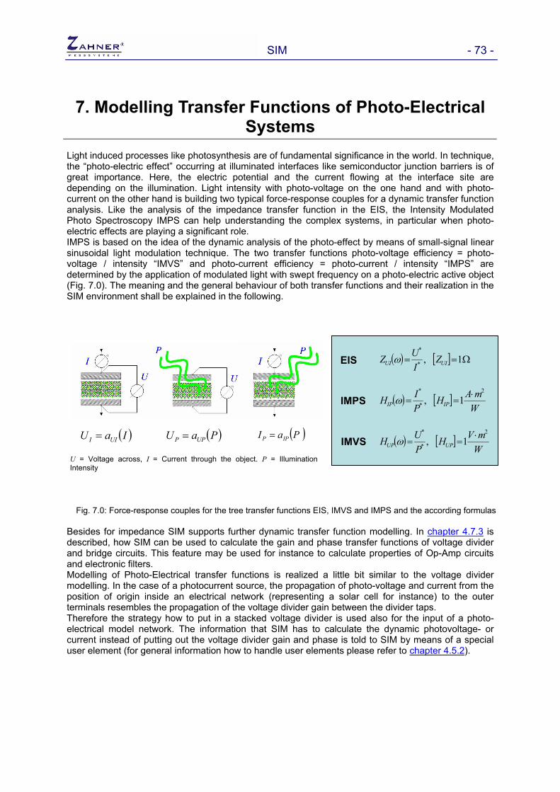
SIM - 73 -
7. Modelling Transfer Functions of Photo-Electrical Systems
Light induced processes like photosynthesis are of fundamental significance in the world. In technique, the “photo-electric effect” occurring at illuminated interfaces like semiconductor junction barriers is of great importance. Here, the electric potential and the current flowing at the interface site are depending on the illumination. Light intensity with photo-voltage on the one hand and with photo-current on the other hand is building two typical force-response couples for a dynamic transfer function analysis. Like the analysis of the impedance transfer function in the EIS, the Intensity Modulated Photo Spectroscopy IMPS can help understanding the complex systems, in particular when photo-electric effects are playing a significant role. IMPS is based on the idea of the dynamic analysis of the photo-effect by means of small-signal linear sinusoidal light modulation technique. The two transfer functions photo-voltage efficiency = photo-voltage / intensity “IMVS” and photo-current efficiency = photo-current / intensity “IMPS” are determined by the application of modulated light with swept frequency on a photo-electric active object (Fig. 7.0). The meaning and the general behaviour of both transfer functions and their realization in the SIM environment shall be explained in the following.
Fig. 7.0: Force-response couples for the tree transfer functions EIS, IMVS and IMPS and the according formulas Besides for impedance SIM supports further dynamic transfer function modelling. In chapter 4.7.3 is described, how SIM can be used to calculate the gain and phase transfer functions of voltage divider and bridge circuits. This feature may be used for instance to calculate properties of Op-Amp circuits and electronic filters. Modelling of Photo-Electrical transfer functions is realized a little bit similar to the voltage divider modelling. In the case of a photocurrent source, the propagation of photo-voltage and current from the position of origin inside an electrical network (representing a solar cell for instance) to the outer terminals resembles the propagation of the voltage divider gain between the divider taps. Therefore the strategy how to put in a stacked voltage divider is used also for the input of a photo-electrical model network. The information that SIM has to calculate the dynamic photovoltage- or current instead of putting out the voltage divider gain and phase is told to SIM by means of a special user element (for general information how to handle user elements please refer to chapter 4.5.2).
( ) [ ]WmAH
PIH IPIP
2
*
*
1, ⋅==ω
( ) [ ]WmVH
PUH UPUP
2
*
*
1, ⋅==ω
( ) [ ] Ω== 1,*
*
UIUI ZIUZ ω
IMPS
IMVS
EIS
( )IaU UII = ( )PaU UPP = ( )PaI IPP =
U = Voltage across, I = Current through the object. P = IlluminationIntensity

SIM - 74 - 7.1 User Elements for the Simulation of Photo-Electrical Processes
The basic purpose of user elements is to realize impedance calculations - not directly supported by the ready made SIM impedance elements - within the support of the simulation and fitting functions of SIM. In this case the user element contains an ASCII text based prescription (written in Thales “andibasic” language), how to calculate the complex impedance from a set of user-defined parameters in dependency of the frequency. This is discussed in chapter 4.5.2 in detail. For modelling of for instance a solar cell, the user element must provide additional functionality:
1. Calculation of a (potentially frequency dependent) photocurrent from a set of user-defined parameters
2. Provision of a flag variable in form of a parameter (an integer between 0 and 2) telling SIM, which type of output magnitude shall be transferred to the calling routine: impedance (Flag=0), photocurrent (Flag=1) or photovoltage (Flag=2).
3. Provision of additional text information telling SIM, which label names have to be used for the physical magnitudes, displayed in SIM result tables and graphic outputs.
4. An assisting code section, not appropriate for user changes, which supports the transfer of intermediate photocurrent and voltage results to the SIM processor.
The realization strategy for an electrical equivalence circuit of a photo-electrical active system usually starts with the circuit element (user element), representing the photo-active process. The strategy is described in the following, starting from the highest simplification. Under small-signal considerations, an “ideal” photo diode behaves as the simplest, straight-forward photo-electrical active object available. It can be understood as a photocurrent generator of infinite source impedance having a current magnitude, defined by just one parameter. Such an object would exhibit infinite high impedance, a constant, frequency-independent photocurrent response and an infinite high photovoltage response. The andibasic source code of a user-element, which simulates such behaviour, is displayed in the following text:
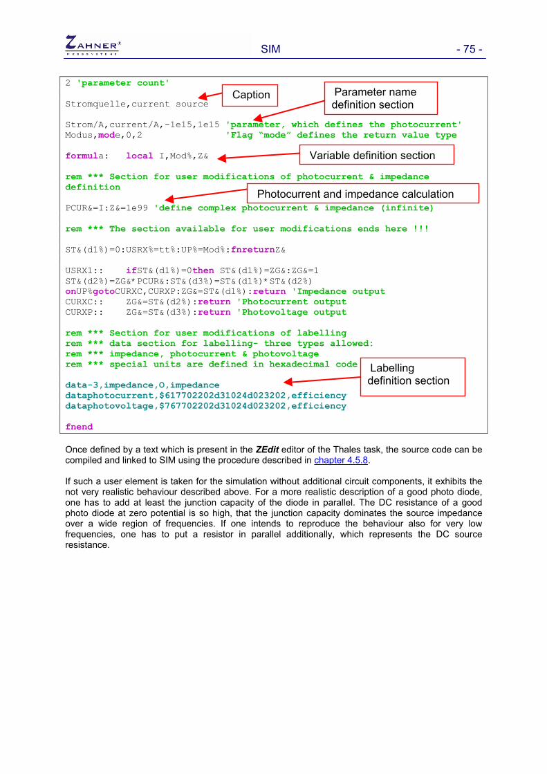
SIM - 75 - 2 'parameter count' Stromquelle,current source Strom/A,current/A,-1e15,1e15 'parameter, which defines the photocurrent' Modus,mode,0,2 'Flag “mode” defines the return value type formula: local I,Mod%,Z& rem *** Section for user modifications of pdefinition PCUR&=I:Z&=1e99 'define complex photocurren rem *** The section available for user modi ST&(d1%)=0:USRX%=tt%:UP%=Mod%:fnreturnZ& USRX1:: ifST&(d1%)=0then ST&(d1%)=ZG&:ZGST&(d2%)=ZG&*PCUR&:ST&(d3%)=ST&(d1%)*ST&(d2onUP%gotoCURXC,CURXP:ZG&=ST&(d1%):return 'ICURXC:: ZG&=ST&(d2%):return 'PhotocurrenCURXP:: ZG&=ST&(d3%):return 'Photovoltag rem *** Section for user modifications of lrem *** data section for labelling- three trem *** impedance, photocurrent & photovoltrem *** special units are defined in hexade data-3,impedance,O,impedance dataphotocurrent,$617702202d31024d023202,efdataphotovoltage,$767702202d31024d023202,ef fnend Once defined by a text which is present in the ZEdit editocompiled and linked to SIM using the procedure described If such a user element is taken for the simulation without not very realistic behaviour described above. For a moreone has to add at least the junction capacity of the diodphoto diode at zero potential is so high, that the junctionover a wide region of frequencies. If one intends to rfrequencies, one has to put a resistor in parallel addresistance.
Caption
Parameter name definition section
Variable definition section
hotocurrent & impedance
Photocurrent and impedance calculation
t & impedance (infinite)fications ends here !!!
&=1 %) mpedance output t output e output
abelling ypes allowed: age cimal code
ficiency ficiency
r of the Thales task, the source code can be in chapter 4.5.8.
additional circuit components, it exhibits the realistic description of a good photo diode, e in parallel. The DC resistance of a good capacity dominates the source impedance eproduce the behaviour also for very low itionally, which represents the DC source
Labelling definition section

SIM - 76 - The following table illustrates the input procedure:
Call the model editor by Create/Edit Model in the SIM menu.
Name the model for instance “Photo”.
Select the User Defined element select Current Source and put in the User Defined Element parameters: 1. initial photo-generated current 2. mode: 0 = impedance 1 = photocurrent 2 = photovoltage
Select New Partial Scheme in order to create the first branch of the schematic.
Select the Capacitor symbol (for the junction barrier capacitance) and enter “300p” for 300 pFarad.
Select Parallel Connection to connect the capacitance in parallel to the user defined element.
Select the Resistor element (for the junction barrier polarization resistance) and enter “10M” for 10 MΩ
Select Parallel Connection to connect the resistor in parallel to the user defined element and the capacitance.
Actual schematic: photodiode (still without a bulk resistance considered)
Fig. 7.1 shows the corresponding equivalent circuit and the course of impedance, photocurrent and photovoltage efficiency spectra. So far, the equivalent circuit could be built up without the usage of partial schemes: the three components, user element as current source, a shunt resistor representing the resistance and a shunt capacitor representing the capacity of the junction barrier are put in parallel.

SIM - 77 -
Fig. 7.1: Impedance spectrum (top), photocurrent efficiency spectrum (middle) and photovoltage efficiency spectrum (bottom) of an ideal photo diode, simulated by means of the equivalent circuit displayed in the inlay of the impedance diagram.

SIM - 78 - The next step into the direction of a more realistic model would be the consideration of the semiconductor bulk resistance. Different from additional parallel circuit components which can be added straight forward, a series component has to be put in by means of a certain sequence, which is identical to the sequence described in chapter 4.7.3 for voltage divider circuits: the series component (or sub-network) has to be defined first as “new partial scheme” (in spite of the fact, that this “sub scheme” may consist of only one component). In the next step it must be combined with the existing circuit by means of the function “connect partial schemes” as “voltage divider”. The following table illustrates, how the input procedure is continued:
Actual Schematic (one branch)
Select the Resistor element (for the semiconductor bulk resistance) and enter “10k” for 10 kΩ
Select New Partial Scheme in order to create a second branch of the schematic.
Actual schematic (two branches)
Now click on Connect Partial Schemes and select Voltage Divider so as to connect the two branches as a voltage divider.
Actual schematic: photodiode including bulk resistance Please note the symbols for the taps on the left hand side. They symbolize the voltage divider ports.

SIM - 79 -
Fig. 7.2: Photocurrent efficiency spectra of an ideal photo diode, simulated by means of the equivalent circuits displayed in the inlays of the diagrams. Upper: without and lower: including consideration of a bulk resistance. Please note the “voltage divider” taps in the lower diagram. Fig. 7.2 shows the corresponding equivalent circuits and the course of the photocurrent efficiency spectra. Proceeding from the actual state of the network in fig. 7.2 lower, further network components appearing in parallel may be added straight forward again, while the introduction of additional serial components have to be considered by beginning new partial schemes. Like demonstrated for the circuit above, the closed partial schemes have to be added to the residual circuit by means of the “voltage divider” operation again. The following table shows, how the existing circuit can be extended by an outer bulk capacity and a network, representing the counter electrode of for instance a Dye Sensitized Solar Cell “DSSC”.

SIM - 80 -
Actual schematic: Photodiode extended with bulk resistance
Select the Capacitor symbol (for the semiconductor bulk capacitance) and enter “100p” for 100 pFarad.
Select Parallel Connection to connect the capacitance in parallel to the residual circuit.
Actual schematic: Photodiode with bulk resistance and bulk capacitance
Select the Capacitor symbol (for the counter electrode double layer capacitance) and enter “180n” for 180 nFarad.
Select New Partial Scheme in order to create a new branch of the schematic.
Select the Resistor element (for the counter electrode charge transfer resistance) and enter “100k” for 100 kΩ
Select Parallel Connection to connect the resistor in parallel to the capacitance.
Select the Resistor element (for the counter electrode electrolyte resistance) and enter “100k” for 100 kΩ
Select Serial Connection to connect the resistor in series to the parallel connection of capacitance and resistor.
Actual schematic (two branches with the schematic of the counter electrode on the right hand)
Now click on Connect Partial Schemes and on Voltage Divider so as to connect the two branches as a voltage divider.
Actual schematic: Simplified Dye Sensitized Solar Cell (DSSC)

SIM - 81 -
Fig. 7.3 Photocurrent efficiency spectra of a photo diode, simulated including the consideration of a bulk resistance (red curve and scheme) and a simplified model of a Dye Sensitized Solar Cell “DSSC” (blue curve and scheme) Fig. 7.3 shows the course of the resulting photocurrent efficiency spectra and the corresponding equivalent circuits. Please note that the numerical values are chosen for a qualitative comparison and not as realistic values relevant for practical samples. The user element #1, linked with the name “current source” into the standard version of SIM looks a little different, compared to the appearance and source code described at the beginning of this chapter. In the following the meaning of these differences is discussed. The actual source code of this “type 2” photocurrent source appears as follows:

SIM - 82 - 4 'parameter count' Stromquelle,current source Strom/A,current/A,-1e15,1e15 'label/unit,range 1.Modus,mode,0,2 'on Modus return impGrenzfrequenz1/Hz,transit frequency1/Hz,1e-15,1e1Grenzfrequenz2/Hz,transit frequency2/Hz,1e-15,1e1 formula: local I,Mod%,Frq1,Frq2,Z& rem *** Section for user modifications of photocu PCUR&=I/csqr(cmplx(1,Tf/(T*Frq2)))/cmplx(1,Tf/( rem *** The section available for user modificati ST&(d1%)=0:USRX%=tt%:UP%=Mod%:fnreturnZ& USRX1:: ifST&(d1%)=0then ST&(d1%)=ZG&:ZG&=1 ST&(d2%)=ZG&*PCUR&:ST&(d3%)=ST&(d1%) onUP%gotoCURXC,CURXP:ZG&=ST&(d1%):re CURXC:: ZG&=ST&(d2%):return 'Photocurrent ou CURXP:: ZG&=ST&(d3%):return 'Photovoltage ou data-3,impedance,O,impedance dataphotocurrent,$617702202d31024d023202,efficiendataphotovoltage,$767702202d31024d023202,efficienfnend The obvious difference is that two additional parameters haphotocurrent. At a closer look on the definition line for thparameters will cause a frequency dependency of the photsimpler model. If the numerical parameter values for bothchosen much higher than the frequencies of interest (eqimaginary contribution in the formula for the photocurrent result of the simpler model. The simpler model “type 1” is t2” as a special case for frequencies much lower than both bOften it is sufficient to model monolithic solar cells witindependent photocurrent source of “type 1”. In contrassemiconductors this does not lead to satisfying results for charge generation and propagation happens distributed ovesimplifying strategy one can take this into account by meffective photocurrent, seen from “outside” of the site of orithe charge carrier lifetime (belonging to transit frequency1) (belonging to transit frequency2) considering the migraticorresponding chain ladder is able to approximate this behaThe usage of the photocurrent source of “type 2” without particular case is disputable for sure. On the other hand it isdue to the embedding network and it is useful for the accordAn alternative analytical model for porous type DSSC will be
Two “breakpoint frequencies” as additional parameters
parameter (photocurrent)' edance,ph.current,ph.voltage 5 'char. frequency1 1.Order 5 'char. frequency2 sqr order
rrent & impedance definition
T*Frq1)):Z&=1e99
ons ends here !!!
*ST&(d2%) turn 'Impedance output tput tput
cy cy
ve influence on the result for the complex e photocurrent one recognizes, that this ocurrent, in contrast to the situation in the “transit frequencies” Frq1 and Frq2 is
uivalent to Tf/T, see chapter 4.5.2), the vanishes and the result is identical to the herefore content in the actual model “type reakpoint frequencies. h the help of one localized, frequency-t at DSSC, which are based on porous the modelling quality, because the photo-r the space zone of a porous system. As a eans of a frequency dependency of the gin. A first order time constant considering and a ½ order (square root) time constant on process of the electrons through the viour with a sufficient accuracy. an explicit proof for the applicability in its well suited for the evaluation of the losses ing efficiency considerations. described later.
Two additional variables
Complex photocurrent calculation

SIM - 83 - 7.2 Analyzing IMPS and IMVS Results of Dye Sensitized Solar Cells
in the Traditional Way by Means of SIM New Solar Cell “SC” technologies allowing cheap mass production by printing, spraying, spin coating, out of roll lamination techniques, flexible shape SC, built under renouncement on clean room procedures are of great demand. Actually the advantages of monolithic SC - high efficiency, clear structure, easy data interpretation – are standing against the still existing disadvantages of the alternative types of SC like the Dye Sensitized SC “DSSC” and Organic SC “OSC”, what are low efficiency, low stability, complex morphology and difficult data interpretation. In a DSSC a highly porous oxide is needed to provide high dye loading for effective light absorption, because the oxide band gap is too wide for visible light. Therefore the electrons, generated by the dissociation of the excitons from photon absorption in dye molecules, have to go long ways to the collecting anode by diffusion through the porous system with a low effective mobility. Photo electron diffusion is in kinetic competition with their recombination at the electrolyte-oxide-interface. The hole transport through a supporting electrochemical reaction adds additional losses. In summary, understanding and optimizing DSSC asks for dynamic, frequency resolved investigation tools like IMPS and IMVS, which were discussed briefly at the beginning of chapter 7. In the traditional DSSC research one is interested in particular on the dominating time constants found in IMPS at short circuit conditions τc and in IMVS at OC conditions τr. It is assumed that the first one is associated to the diffusion kinetics of the photo electron charge and the second one is associated with the recombination reaction. The term ηd = 1 - τc/ τr determines the dynamic efficiency regarding the competition between recombination and diffusion. Analyzing the dynamic properties should therefore provide useful information for SC optimizing. Fig. 7.4 shows and IMPS and an IMVS spectrum of a Zinc Oxide based DSSC as a typical example.
Fig. 7.4: Dynamic efficiency spectra measured on a ZnO based DSSC in Bode representation, on the left IMPS
(under short circuit condition), on the right IMVS (under open circuit condition). For an accurate determination of a single time constant from an experimental spectrum it is not necessary to describe the DSSC by means of a sophisticated model. It is therefore sufficient only to use the current source of “type 2”, which is content of the standard user element library for the simulation. The procedure is shown in the following table:

SIM - 84 -
Call the model editor by Create/Edit Model in the SIM menu.
Name the model for instance “Photo”.
Select the User Defined element select Current Source and put in the User Defined Element parameters: 1. initial photo-generated current 2. mode: 0 = impedance (not necessary for the traditional way) 1 = photocurrent (for the IMPS spectrum) 2 = photovoltage (for the IMVS spectrum) 3. transit frequency1 (for evaluation of the time constants τc & τr) 4. transit frequency2 (for additional refinement)
Select New Partial Scheme in order to create the first branch of the schematic.
Actual schematic: Photocurrent source with breakpoint frequencies
Fig. 7.5 shows the result, when the current source “type 2” is applied and fitted to the spectra measured on a Zinc oxide based DSSC.
Fig. 7.5: Analysis of the dynamic efficiency spectra of a ZnO based DSSC in Nyquist representation. The circles indicate the measurement samples; the solid line curves the simulated spectra, modelling the electron diffusion
and recombination time constants τc and τr. On the left the IMPS with the breakpoint frequency 1/(2πτc) is depicted, on the right the IMVS with 1/(2πτr).
In this example the time constants are found to τc ≈ 360 µs and τr ≈ 24 ms and the dynamic efficiency ηd = 1 - τc/ τr is ηd ≈ 0.985.

SIM - 85 -
7.3 Setting up SIM to the Joint Fitting Procedure “TRIFIT” for EIS, IMPS and IMVS Spectra
A special fitting feature of this program is the so called “TRIFIT-algorithm”. It allows the joint best model fit of the three types of experimental data from impedance, dynamic photocurrent- and photo voltage efficiency spectra, which were acquired all from the same system state of the object under test. Compared to the analysis of the isolated spectra, like it is popular in EIS fields, the relation between the number of known observables and the number of free parameters is increased. This leads to a model close to definiteness with less ambiguity. A successful modelling process for EIS analysis usually consists of a loop sequence of manual model refinement via trial and error until a certain degree of perfection is reached. It is followed by a final automatic optimization, which is performed by the fitter program. The same procedure results in an extremely laborious process, if this strategy is used for the development of a common model, which has to fit impedance, IMVS and IMPS spectra in parallel of the same system under test: Due to differing significance of the parameters in different transfer functions, a sequential try and error adaptation will always minimize the deviations for one type for the cost of increasing deviation for the two remaining types. A synchronisation of this process for the three types in order to find a common best fit is nearly impossible under these circumstances. To solve this problem, SIM provides the TRIFIT procedure. Here all parameters of a common model for the three types of transfer functions can be fitted synchronously into the direction of a common optimum. One prerequisite of TRIFIT is, that by means of the special user elements discussed above, a model can be designed, which is able to calculate impedance as well as IMPS/IMVS results. The second base of TRIFIT is the possibility of SIM to handle several models together with several experimental data sets in parallel. To set up SIM for a joint fitting procedure of EIS, IMPS and IMVS spectra, three copies of the same model must exist in the memory of SIM. In the first one, the switching flag variable “mode” is set to zero, forcing impedance as result. The experimental samples of the objects EIS spectrum have to be assigned to this model copy. In the second one, “mode” is set to one, forcing the dynamic photocurrent as result. The experimental samples of the objects IMPS spectrum have to be assigned to this model copy. In the last one, “mode” is set to two, forcing dynamic photo voltage as result. The experimental samples of the objects IMVS spectrum have to be assigned to the third model copy. All three model copies have to be present at the beginning of the SIM model table in the sequence depicted above. In chapter 4.4 it is described, how models may be moved or deleted within the SIM memory, so as to establish a certain sequence order (chapter 3.4 for experimental spectra). Chapter 5.2 explains the assignment procedure of experimental data sets to particular models. As soon as this set up is complete, SIM can be switched to the TRIFIT mode. When activated, on call the fitter performs the fitting procedure different in some important details from the general strategy described in chapter 5.3:
1. The fitting procedure is not only applied to one model (normally the one which is activated, or the first one of the list, if more than one are activated), but extended to at least two or up to three models (from the first three ones, as stated above).
2. The fitting error (the magnitude, which is minimized in the fitting progress) is calculated from the deviations of all active models in correlation with their individually assigned experimental samples.
3. The fitter varies and synchronizes all parameter sets forcing common values, except for the “mode” flags.
At the end of the fitting procedure all active models exhibit (apart from the “mode” flag) the same optimized parameter set. In TRIFIT mode, editing a parameter of a certain model will be automatically extended to the remaining active models. If one deactivates TRIFIT, the three model types can be handled, checked and modified individually again.

SIM - 86 - A useful plan for a successful modelling of impedance and photoelectric properties for instance of solar cells may look like follows:
1. Provide the experimental spectra of all valid types of your system under test in the measurement section of SIM.
2. Begin with the development of an impedance model containing the user element for a photocurrent source located in the centre of the network.
3. Use your existing knowledge to approximate the observed spectra shape of the experimental data by stepwise modifications, like you would proceed with a single EIS object too.
4. As soon as the model is able to roughly reproduce the characteristics of the experimental EIS data, use the “select new model” function, chapter 4.8, and copy the EIS model as a second version for the photocurrent, and, if necessary, as a third version for the photovoltage modelling.
5. Assign the experimental data of IMPS (and, if necessary IMVS) to the model copies like described in Chapter 5.2.
6. Finally, set the TRIFIT mode (Fig. 7.6) and call the fitter.
Left: In the TRIFIT menu you may switch on or off the TRIFIT mode. Please recognize that a common fit must include EIS and IMPS data. IMVS data may be omitted. Selection of the TRIFIT Off button returns SIM to the normal mode.
Fig. 7.6: TRIFIT selection menu As an application example for training, the directory “c:\thales\examples\spectra” contains three measured spectra (EIS, IMPS and IMVS) of a SC, “1_solarcell.ism” to “3_solarcell.ism” and accordingly the folder “c:\thales\examples\models” provides three model files “1_solarcell.isf” to “3_solarcell.isf”.

SIM - 87 -
8. SIM Setup During the start up of SIM a couple of parameters will be set to default values. This set of parameters includes both, mathematical settings as well as presets of the graphical display routines. Mathematical parameters are e.g. the width of the smoothing window and the criterion of convergence of the fitter. Graphical presets include the display mode and the scaling options. In order to offer different settings of the program which may be changed by the user, the presets may be saved and loaded. To save, load and edit the SIM parametersa click on the Hippo icon.
8.1 Save To save a certain preset of the simulation program select the 'save' option of the preset menu. An input box will prompt and demand the input of a filename. The length of the filename of a preset file is restricted to 5 characters. Put in a filename or cancel the saving option by use of the <escape>-function. To save the preset confirm the filename, e.g. 'bode1', and the program will generate a preset file named 'supbode1' ( sup = set up ). Putting in no filename at all will generate a preset file named 'sup'.
8.2 Recall To load a certain preset select the 'recall'-option of the preset menu. An input box will prompt and demand the input of a filename. Put in the filename or cancel the recall option by use of the <escape>-function. To load a preset confirm the filename, e.g. 'bode1', and the program will load the corresponding preset file named 'supbode1'. Putting in no filename at all will recall the preset file named 'sup'.
8.3 Edit The 'edit'-option offers the input of one parameter - the criterion of convergence of the fitter. All other parameters that will be saved must be altered in the corresponding subroutines, e.g. the width of the smoothing window, display mode, display options, scaling options, etc.
CPE reference frequency / Hz Defines the reference frequency for CPE elements (Hz) Min. fitting success Defines the limit at which the fitter stops Phase weighing Max. count of spectra/models Defines how many spectra and models are allowed to be
loaded to RAM

SIM - 88 - Max. count of I/E curves Defines how many I/E curves are allowed to be loaded
to RAM Max. count of CV curves Defines how many CV curves are allowed to be loaded
to RAM Smooth sample count Defines the width of the smooth window (samples) Export comments (0=no) 0 = no comments are exported in an ASCII list Graphic export symbol size Defines the size of the symbols for the export of a graph Label for impedance Defines the label for the impedance Label for admittance Defines the label for the admittance Use export format 0 = standard graphic with y-axis label on top
1 = export graphic with y-axis label vertical
9. Init SIM
A click on this button deletes all measurement data and model data from the RAM and initializes the SIM parameters. Click this button for a “cold start” of SIM.