Text: Pictures: Magnus Bergmar & Marlene Winberg Jan-Åke ...

Presented by
Simon Winberg
Attribution-ShareAlike 4.0 International (CC BY-SA 4.0) Planned to be double period lecture

Terms: Temporal vs spatial, data path
General processor types (JvN vs Harvard)
Datapath design
Instruction Set Architecture
Instruction Path
Micro instructions
Processor aspectsCISC vs RISC
Sources Acknowledgement:Lecture based on the book Logic and Computer Design Fundamentals, Fifth Edition, by Mano, Kime & Martin. Pearson. 2016.
next
lectu
re


Temporal Computation Spatial Computation
The traditional paradigm
Typical of Programmers
Things done over time steps
Suited to hardware
Possibly more intuitive?
Things related in a space
A = input(“A= ? ”);
B = input(“B =? ”);
C = input(“B multiplier ?”);
X = A + B * C
Y = A – B * C
A?
B?
C?
+ *
X !
Y !
-
Which do you think is easier to make sense of?
Can provide a clearer indication of relative
dependencies.

Definition: data path or datapath This is the set of functional units that carry out
data processing operations for a computer system. The datapaths, together with a control unit and
ALU, makes up the CPU of a computer. Larger datapath (or composite datapaths) can be
created by joining more than one together using (e.g.) multiplexers.
Reconfigurable datapaths* : These are datapaths that can be re-purposed at
run-time using a programmable fabric e.g. may allow for more efficient processing and substantial power savings for particular types of application.
* Source: https://en.wikipedia.org/wiki/Datapath
data
source
data
destination
data

Types of Processor ArchitectureEEE4120F
Type
A
Type
B
Type
C
Type
D
Type
E
Type
F
Type
G
Type
H
Type
I
Type
J
(reminders)

Named after John von Neumann A Hungarian mathematician. He was
the first to write about requirements foran electronic computer (done in 1945).
The ‘von Neumann computer’ differed from earlier computers that were programmed by hard wiring.
Most computers since then have been inspired from this design.

The von Neumann computer comprises the following four components:
Memory
Control Unit
Arithmetic LogicUnit (ALU)
Input/Output
Figure 1: The Von Neumann architecture*
* image adapted from http://en.wikipedia.org/w/index.php?title=Von_Neumann_architecture
The ‘JvN Machine’
We will generally be using this model
for a CPU design…

Random access, read/write memory stores both programs and data
Program comprises instructions (von Neumann termed ‘machine instructions’) that tells the computer what do.
Data is simply information to be used by the program

Control unit fetches instruction or data from memory, decodes and executes the instruction, sequentially completes sub-operations for the instruction
Arithmetic Logic Unit does basic arithmetic operations (earlier CPUs didn’t have multiply or divide; had few instructions, e.g. LOAD, STORE, ADD, IN, OUT and JUMP on flags) and logic operations (e.g. AND, OR, SHIFT etc.)
Input/Output interfaces to other systems and the human operator

Simple recap of Von Neumann Arch: http://www.youtube.com/watch?v=DMiEgKZ-qCw
Some history of Von Neumann leading towards his machine: (not examined!)
“The Greatest Computer Programmer Was Its First”http://www.youtube.com/watch?v=Po3vwMq_2xA

The Harvard ArchitectureEEE4120F
The Big Competitor…

The Harvard architecture physically separates storage and signal lines for instructions and data.
The term originated from the “Harvard Mark I” relay-based computer that stored instructions on (24-bits wide) punched tape and data in electro-mechanical counters.
Data storage entirely contained within the central processing unit, and provided no access to the instruction storage as data.
(for the original MarkI) programs needed to be loaded by an operator as the processor could not initialize itself.
ALU
Control
UnitInstruction memory
Data memory
I/O
Nowadays this general architecture (albeit greatly
enhanced) is still relevant! They are technically
referred to as “modified Harvard architecture”. Many
processors today (especially embedded ones) still
implement this separation of data and storage for
performance and reliability reasons. Harvard
Architecture

“Harvard Mark I”
https://www.youtube.com/watch?v=4ObouwCHk8w

…
The Modified Harvard Architecture (MHA) is about the most ubiquitous for low-cost microcontrollers
Main feature of the MHA:
Allows program memory to be read… or
May even allow program memory to be written…
But reprogramming flash is not necessarily just
a matter of writing an address (and the potential
for a simple mistake like M[0x0] = 0).
It usually needs a process to be followed, e.g.:
erases block, put data in write buffer, call the
routine that talks to flash to write the block of
memory.
Your’re probably thinking
“Eeek! No way?!”That is surely just JvN anyway?


You already know about the ARM architecturee.g. flavours by STM, Texas Instruments,
NXP/Freescale, Intel… For which TSMC (Taiwan Semiconductor
Manufacturing Company) and the GlobalFoundries manufacture most of the actual chips.
But these microcontrollers you should also know about PIC (Peripheral Interface Controller) AVR
PIC and AVR are essential for designing low-power, low-cost systems!

PIC Developed by Microchip Technology
(Derived from the PIC1650 originally designed by General Instrument's Microelectronics Division)
Available since 1976* Some use pure Harvard Architecture, i.e. program memory is
protected; others Modified Harvard where the program memory can be read (and sometimes even written)
All models use flash memory for program storage Low cost, low power, ease of reprogramming with built-in
EEPROM Abundant development tools and application notes Often marketed as “PICmicro” A long history of use, probably the most used microcontroller
of all time!
* Information source: https://en.wikipedia.org/wiki/PIC_microcontrollers

AVR – “Alf and Vegard's RISC processor” Modified Harvard architecture 8-bit RISC Even lower power options, generally low cost (maybe the
cheapest AVR is not as cheap as the cheapest PIC) ATmega328P one of the most popular, very low power but
fairly powerful micros Major claim to fame: one of the first micros to have on-chip
flash, instead of one-time programmable ROM or hassles of using EEPROM
Inspiring historical fact: The AVR architecture was conceived by two students from
the Norwegian Institute of Technology (NTH), Alf-EgilBogen and Vegard Wollan*
The name “AVR” is commonly thought to stand for “Alf and Vegard's RISC processor”
* Information source: https://en.wikipedia.org/wiki/AVR_microcontrollers

- Coffee percolator
- ABS brakes
- Radio control of a model airplane
- Car radio (e.g., auto tuning, stored stations)
- Washing machine
- Portable battery-operated game console
- Weather sensor
- Garage door opener
- iPod
- Burglar alarm
- Radar car speed sensor
- Wireless network switch
Which of these applications might you instead use an Intel 8051,
AVR or PIC? Or even some other option.
ARMWhich of these applications do you think a ARM
would be suited to?

Suggested processor choices
I’d probably make the following choices…
- Coffee percolator - PIC
- ABS brakes - ARM or AVR
- Radio control of a model airplane – PIC or AVR
- Car radio – PIC for auto turning feature at least
- Washing machine – Probably a PIC
- Portable battery-operated game console - ARM
- Weather sensor – PIC (lowest power options, usually doesn’t need speed)
- Garage door opener – PIC or AVR, something cheap
- iPod – ARM
- Burglar alarm - probably a PIC, if there’s not much signal processing
- Radar car speed sensor – probably a DSP and an ARM or PIC for comms
- Wireless network switch – perhaps a ARM or something super fast, like DSP
Which of these applications might you instead use an Intel 8051,
AVR or PIC? Or even some other option.
Class activity – to ARM or not to ARM sample solution & discussion

⚫ In a wide range of embedded
computers and control systems e.g.
⚫Highly reliable – ABS, hard drives
⚫Consumer – cameras, PDAs
Cell phones (e.g. Nokia N series, Sony K series)
⚫ Game systems (Nintendo DS, etc)
⚫ Network systems (routers, switches, firewalls, etc)
Nintendo DSCellphone iPod Network switch
ABS breaking

data source data destination
data

A processor design can be considered as comprising
Datapath: moving data/signals around; and
Control: making decisions (e.g. whether or not to do an operation) and doing operations (e.g. adding two registers)

The specification of a computer is provided by defining its appearance to the programmer at its lowest level, its Instruction Set Architecture (ISA) level

The specification of a computer is provided by defining its appearance to the programmer at its lowest level, its Instruction Set Architecture (ISA) level
From the ISA the computer architecture is developed…
Computer architecture development essentially involves deciding its datapath and control.
Is effective approach for also designing a processor/CPU or designing a special-purpose application accelerator or co-processor

DatapathsMost generally this refers to the registers,
processing units, and interconnections(busses) that are used to process and transfer data in a computer system
Datapath comprisesA set of registers (that store data)Microoperations to perform operations on data
stored in the registersControl interfaces (for sequencing and
arbitrating operations)
Recommended video: “How a datapath works inside a computer
system“. Available at: https://youtu.be/ibYYqvp9FmU

Keep that in the back of your mind while we will look into the
digital circuit mechanisms for how an instruction is decoded,
data gathered, operations invoked, and results stored…
Hopefully this will give you detailed understanding of the CPU
workings so that you can develop your own ☺
You presumably remember the cycle:
1) Fetch
2) Decode
3) Execute
Coverd in EEE3095/6S

Datapath design is
largely about the
circuitry to store
data and to select
and connect data to
be transferred
between processing
units in a processor
select data
processing unit
selecting
select data to transfer
connecting
selectingselecting
connect
connect
connect
store
connect
Will briefly explain the parts…processing
unit
Example of a Datapath
Based on CH8 Fig. 8-1 of Logic and Computer Design Fundamentals, Fifth Edition, by Mano, Kime & Martin. Pearson. 2016.
Onwards to….
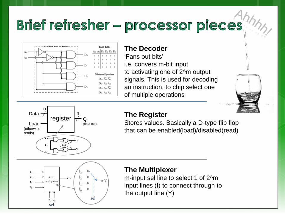
The Decoder‘Fans out bits’
i.e. convers m-bit input
to activating one of 2^m output
signals. This is used for decoding
an instruction, to chip select one
of multiple operations
registerLoad
(otherwise
reads)
Datan
Q(data out)
n The RegisterStores values. Basically a D-type flip flop
that can be enabled(load)/disabled(read)
The Multiplexerm-input sel line to select 1 of 2^m
input lines (I) to connect through to
the output line (Y)
I3
I2
I1
I0
Y
sel
sel

General Computer
Architecture comprises:
• Instruction Set Architecture*
• Storage Resources:
• Instruction memory,
• Data memory,
• Register file,
• Program counter
• Datapath:
• Runs instructions
and activates the
processes
…
Based on CH8 of Logic and Computer Design Fundamentals, Fifth Edition, by Mano, Kime & Martin. Pearson. 2016.

General Computer Architecture is
designed around / comprises:
• Instruction Set Architecture*
• Storage Resources: • instruction memory,
• data memory,
• register file,
• program counter
• Datapath: runs the instructions and
activates processes Block diagram of a single cycle computer
Instruction Set Architecture (ISA) =
• Instruction format: how the instructions are structured, how the
bits of the instruction link to operations/data
• Instruction specification: describe each of the available
instructions that the system can execute.
* we delve into detail later in the course
An example instruction format that is likely used for arithmetic/logic operations on a RISC processor
Based on CH8 Fig. 8-15 of Logic and Computer Design Fundamentals, by Mano, Kime & Martin. Pearson. 2016.

Function Unit (FU)
(or ‘execution unit’)
• Carries out the operations
• Could be structured in
various ways.
• Typically…
FU = ALU + CU
and possibly
FUmain = Σ (FUsubunits )
for a multi-processor system
Block diagram of a single cycle computer
Based on CH8 Fig. 8-15 of Logic and Computer Design Fundamentals, by Mano, Kime & Martin. Pearson. 2016.
As show in this diagram, the FU has two input registers, A and B, that it operates on.There is a Function selector (FS) input used to chose the operation to perform. When this operation is performed, the result output is latched to F and updates status flags V,C,N,Z.The MD (memory data) select can bypass the FU if the instruction is loading from memory.
This used for a store instruction, i.e. using A as address and B as data to write to the address

The Arithmetic/Logic Unit (ALU)
Arithmetic operations: + - * /
Logic operations: and, or, xor, not
The ALU has
• Inputs to provide data to be
processed as well as
• Input for type of operation to be
performed, (e.g. if it needs to do an
ADD or AND, etc.)
• Has outputs that provide the
results of the operation (G output
in figure).
• Output flags, e.g. carry (C) output
flag that stores status information
of the operation (e.g. carry flag set)
or error states (divide by zero). An n-Bit ALU
Based on CH8 Fig. 8-2 of Logic and Computer Design Fundamentals, by Mano, Kime & Martin. Pearson. 2016.

Control Unit (CU)
The CU is the part of the CPU that directs the working of the processor.
The CU coordinates the computer's memory, ALU and its input and output devices, making these parts respond to program instructions.
Control Unit: can be abstracted as the circuitry used to sequence and control the system (this simplification obviously hides many aspects such as memory and IO)
Sometimes the control unit is not shown in the design of a computer (or cannot be shown as a distinct subsystem) as it may be distributed through the system, closely integrated within other components; this is particularly the case for highly complex pipelined architectures where it is difficult to have a separate component to arbitrate the system.

Based on CH8 Fig. 8-1 of Logic and Computer Design Fundamentals, Fifth Edition, by Mano, Kime & Martin. Pearson. 2016.
We’ve looked at the
datapath to connect
the pieces, the
register file, the ALU,
the FU, the CU.
Now you hopefully have an
inkling of how the pieces
work together to 1) get data
to the FU inputs, 2) grab
results from FU, 3) move
FU results/memory to
register or memory address
Don’t be too worried yet: we are going to
map out an instruction to the datapath… select data
processing unit
selecting
select data to transfer
connecting
selectingselecting
connect
connect
connect
store
connect
processing
unit
Example of a Datapath

How an instruction is executed
Arithmetic
Logic Unit
(ALU)
A
B
Cin
S
Y
Cout
Z
n
n
select function
carry input
B data in
A data in
result
output Y
carry
out
zero
out
Selecting
where Y will
be sent
Selecting
where A
comes from
Selecting
where B
comes from
Selecting operation to perform, this
may or may not activate the ALU (e.g.
for LOAD the ALU might do nothing)
SA circuitry will select the
right source register and
connect it to A
SB circuitry will select the
right source register and
connect it to B
Cin for a simple processor
will just connect to a D FF
that remembers the last
carry state.
The Opcode part of the
instruction will link to a decoder
(and some other logic) and
select the correct ALU option –
for some opcodes the ALU just
does a NOP or passthrough.
n DR circuitry will select the
right destination to send
the result (Y) of the ALU
(this may be to memory)
Carry output might be send
somewhere else, but usually
to a D FF which loops back as
input for the next instruction
The zero out flag might activate
further things but probably also
loops back to the input for the
next instruction.
But before we get into this…


Micro instructions
As a means plan and design an instruction set
Micro instructions
Major instruction
Ahmadal’s test

FREE Creative Commons License
COUNTRY BOY
Music: https://www.bensound.com
Next up: instruction path
micro-instructionsCache hierarchy, shared memory
I suggest taking a break and stretch a bit if you are planning
to directly proceed with the next presentation.

Image sources:
Clipart sources – public domain CC0 (http://pixabay.com/)
datacenter image – pixabay
ant – needpix.com
commons.wikimedia.org
images from flickr
Disclaimers and copyright/licensing details
I have tried to follow the correct practices concerning copyright and licensing of material,
particularly image sources that have been used in this presentation. I have put much
effort into trying to make this material open access so that it can be of benefit to others in
their teaching and learning practice. Any mistakes or omissions with regards to these
issues I will correct when notified. To the best of my understanding the material in these
slides can be shared according to the Creative Commons “Attribution-ShareAlike 4.0
International (CC BY-SA 4.0)” license, and that is why I selected that license to apply to
this presentation (it’s not because I particulate want my slides referenced but more to
acknowledge the sources and generosity of others who have provided free material such
as the images I have used).


![Ocw [animal reproduction]](https://static.fdocuments.us/doc/165x107/58835b371a28ab42678b649f/ocw-animal-reproduction.jpg)