
Silver-coated elevated bowtie nanoantenna arrays ... · Silver-Coated Elevated Bowtie Nanoantenna...
21
Silver-coated elevated bowtie nanoantenna arrays: Improving the near-field enhancement of gap cavities for highly active SERS Lei Feng, Renping Ma, Yandong Wang, Daren Xu, Dongyang Xiao, Lingxiao Liu, and Nan Lu ( ) Nano Res., Just Accepted Manuscript • DOI 10.1007/s12274-015-0871-2 http://www.thenanoresearch.com on July 31, 2015 © Tsinghua University Press 2015 Just Accepted This is a “Just Accepted” manuscript, which has been examined by the peer-review process and has been accepted for publication. A “Just Accepted” manuscript is published online shortly after its acceptance, which is prior to technical editing and formatting and author proofing. Tsinghua University Press (TUP) provides “Just Accepted” as an optional and free service which allows authors to make their results available to the research community as soon as possible after acceptance. After a manuscript has been technically edited and formatted, it will be removed from the “Just Accepted” Web site and published as an ASAP article. Please note that technical editing may introduce minor changes to the manuscript text and/or graphics which may affect the content, and all legal disclaimers that apply to the journal pertain. In no event shall TUP be held responsible for errors or consequences arising from the use of any information contained in these “Just Accepted” manuscripts. To cite this manuscript please use its Digital Object Identifier (DOI®), which is identical for all formats of publication. Nano Research DOI 10.1007/s12274-015-0871-2
-
Upload
duongkhanh -
Category
Documents
-
view
223 -
download
0
Transcript of Silver-coated elevated bowtie nanoantenna arrays ... · Silver-Coated Elevated Bowtie Nanoantenna...

Nano Res
1
Silver-coated elevated bowtie nanoantenna arrays:
Improving the near-field enhancement of gap cavities
for highly active SERS
Lei Feng, Renping Ma, Yandong Wang, Daren Xu, Dongyang Xiao, Lingxiao Liu, and Nan Lu ( )
Nano Res., Just Accepted Manuscript • DOI 10.1007/s12274-015-0871-2
http://www.thenanoresearch.com on July 31, 2015
© Tsinghua University Press 2015
Just Accepted
This is a “Just Accepted” manuscript, which has been examined by the peer-review process and has been
accepted for publication. A “Just Accepted” manuscript is published online shortly after its acceptance,
which is prior to technical editing and formatting and author proofing. Tsinghua University Press (TUP)
provides “Just Accepted” as an optional and free service which allows authors to make their results available
to the research community as soon as possible after acceptance. After a manuscript has been technically
edited and formatted, it will be removed from the “Just Accepted” Web site and published as an ASAP
article. Please note that technical editing may introduce minor changes to the manuscript text and/or
graphics which may affect the content, and all legal disclaimers that apply to the journal pertain. In no event
shall TUP be held responsible for errors or consequences arising from the use of any information contained
in these “Just Accepted” manuscripts. To cite this manuscript please use its Digital Object Identifier (DOI®),
which is identical for all formats of publication.
Nano Research
DOI 10.1007/s12274-015-0871-2

TABLE OF CONTENTS (TOC)
Silver-Coated Elevated Bowtie Nanoantenna Arrays:
Improving the Near-field Enhancement of Gap
Cavities for Highly Active SERS
Lei Feng, Renping Ma, Yandong Wang, Daren Xu,
Dongyang Xiao, Lingxiao Liu, and Nan Lu*
State Key Laboratory of Supramolecular Structure and
Materials, Jilin University, Changchun 130012, China
Silver-coated elevated bowtie nanoantenna (SCEBNA) array is a
highly active SERS substrate due to the improvement of the hot-spot
intensity caused by the integrated contribution of the "lightning rod"
effect, the resonance coupling, and the formation of the plasmonic
Fabry-Pérot cavity.
Nan Lu, [email protected]

Silver-Coated Elevated Bowtie Nanoantenna Arrays:
Improving the Near-field Enhancement of Gap Cavities
for Highly Active SERS
Lei Feng§, Renping Ma§, Yandong Wang, Daren Xu, Dongyang Xiao, Lingxiao Liu, and Nan Lu ( )
Received: day month year
Revised: day month year
Accepted: day month year
(automatically inserted by
the publisher)
© Tsinghua University Press
and Springer-Verlag Berlin
Heidelberg 2014
KEYWORDS
SERS,
surface plasmon
resonance,
bowtie nanoantenna,
nanosphere lithography,
gap cavity
ABSTRACT
Improving the hot-spot intensity is a key issue in surface-enhanced Raman
scattering (SERS). Bowtie nanoantenna (BNA) is an effective device to
concentrate light energy into nanoscale volume and produce strong hot spots.
Nanosphere lithography (NSL) is a large-area and low-cost technique to
produce BNA arrays, while the SERS activity of NSL-fabricated BNAs is
limited. In this paper, we present a facile method to improve the SERS activity
of the conventional NSL-fabricated BNAs by transforming the geometry. The
new configuration is termed the silver-coated elevated bowtie nanoantenna
(SCEBNA). The SCEBNAs perform intensive near-field enhancements in the
gap cavities due to the integrated contribution of the "lightning rod" effect, the
resonance coupling, and the formation of the plasmonic Fabry-Pérot cavity. The
experimental measurements and the finite difference time domain simulations
reveal that the hot-spot intensity and the substrate enhancement factor can be
optimized by adjusting the silver thickness. The optimal sample is of a
capability of trace-amount detection with fine reproducibility.
Benefiting from recent development in
nanofabrication and the ongoing studies about
plasmonics, surface-enhanced Raman scattering
(SERS) spectroscopy has been a powerful technique
in chemical and biological sensing due to its
ultrasensitivity and the capability to provide
molecular fingerprint [1-6]. One key issue of SERS in
the practical application is the fabrication of highly
active and reproducible substrates [7, 8]. According
to the electromagnetic mechanism, the substrates
employ those sites with tiny volume and extremely
concentrated electromagnetic fields to excite the
remarkable Raman radiation of the adsorbed
molecules, and these sites are termed the hot spots
Address correspondence to Nan Lu, [email protected]
Nano Research
DOI (automatically inserted by the publisher)
Research Article
| www.editorialmanager.com/nare/default.asp
2 Nano Res.
[9-11]. It has been experimentally demonstrated that
only 1% molecules at the hot sites with an
enhancement factor (EF) larger than 107 can
contribute almost 70% to the overall SERS signal on
the silver-film-over-nanospheres substrate [12]. This
result illuminates the significance of increasing the
hot-spot intensity for improving the average EF of
the substrate [13].
Noble-metal bowtie nanoantenna (BNA) can
serve as a device that confines and localizes the
optical radiation into nanoscale volume performing
excellent field concentration [14, 15]. It has been
applied in not only surface-enhanced spectroscopies
[16-19], but also nonlinear optics [20-22], optical
tweezers [23], photocatalysis [24], and biosensing [25].
All these applications depend on the hot spots near
the gap between the two adjacent triangle tips where
the "lightning rod" effect and the resonance coupling
take place [11, 26, 27]. The "lightning rod" effect is a
frequency-independent phenomenon where the local
charge is fiercely compressed at the triangle tips
under the excitation of electromagnetic waves
polarized along the tip axis, and thus the local fields
in the vicinity of the tips are enhanced [28, 29]. The
resonance coupling is the interaction of the
frequency-dependent plasmon resonance of the two
individual nanotriangles. According to the plasmon
hybridization theory, the large field enhancement in
the gap results from the admixture of the
higher-order multipolar resonances of each
individual nanotriangle into the bonding dipolar
dimer modes of the BNA [30]. Decreasing the
separation of the two nanotriangles, more
higher-order multipolar resonances can contribute to
that admixture. So the hot-spot intensity can be
enhanced by minimizing the radius of curvature of
the tips and the gap size. Much technical effort has
been devoted to the fabrication of the subtle features,
whereas the high-precision fabrication techniques are
difficult and time-consuming [18-20, 26, 31-34].
Moreover, shrinking the gap volume means
decreasing the probability of the Raman molecules to
be assembled onto the hot-spot region, which goes
against the performances of the SERS substrates
especially for low-concentration and reproducible
detections [5, 8, 35]. Transformation of the BNA
geometry is another solution to improve the hot-spot
intensity. Schuck et. al. reported an evolved
configuration termed the "asymmetric bowtie
nano-colorsorters", where two BNAs are oriented in a
"cross" configuration. The additive BNA induces a
new coupling regime causing a further enhancement
of the gap fields by adjusting the symmetry of the
system [36]. Gu’s group fabricated the elevated BNA
which is a BNA held by two underlying silicon
pillars [17]. This configuration can reduce the
substrate effect by exposing a larger volume with
enhanced fields to excite the Raman scattering of
molecules [37]. Besides, the silicon pillars hold the
localized surface plasmon (LSP) of the BNA near to
the anti-node of the standing-wave in the Fabry-Pérot
cavity [17, 38-40]. This generates more efficient
excitation of the bowtie LSP and thus stronger hot
spots.
BNAs either with subtle features or evolved
configurations are usually fabricated using the
scanning beam lithography (SBL) [41]. SBL can be
used to precisely produce nano-bowties with a high
resolution and an arbitrary variation of the
geometrical parameters. While as a serial technique,
the high cost and the low throughput limit its
extensive uses. Nanosphere lithography (NSL) is
another technique which can be used to fabricate
BNA arrays in a large area with high throughput and
low costs, but the geometrical parameters are limited.
For example, the gap size and the triangle size of the
bowtie restrict each other. As mentioned above, to
satisfy an efficient resonance coupling, the gap size
should be small enough [30], which demands a small
diameter of the closely packed nanospheres. But, for
sufficient higher-order multipolar resonances of each
nanotriangle to couple with the bonding dipolar
mode, the triangle size can't be too small [30], which
demands relatively large nanospheres. This intrinsic
conflict limits the EF of NSL-fabricated BNAs inferior
to the order of ~108, typically 107 [42].
Therefore, the parallel fabrication of
BNA-based structures performing an improved field
enhancement with no need for the subtle features, e.g.
sub-10-nm gaps [17], is significant in the practical
applications of highly sensitive SERS. Herein we
demonstrate a method using NSL to produce an

www.theNanoResearch.com∣www.Springer.com/journal/12274 | Nano Research
3 Nano Res.
evolved configuration of the BNA, i.e. the
silver-coated elevated bowtie nanoantenna
(SCEBNA). The SERS activity of the SCEBNAs is
superior to conventional NSL-fabricated BNAs.
Intensive hot spots, locating at the gaps with a few
tens of nanometers, can be generated due to the
integrated contributions of the “lightning rod” effect,
the resonance coupling, and the formation of the
plasmonic Fabry-Pérot cavities. We investigated the
dependence of the hot-spot intensity on the thickness
of the silver coating. The optimized substrate is
highly SERS active showing a capability of trace
amount detection with fine reproducibility.
Fig. 1 shows the fabrication process of the
SCEBNA. We first prepared a self-assembled
monolayer (SAM) of close-packed polystyrene (PS)
nanospheres on the Si substrate as described
elsewhere [43]. The diameter of the PS spheres is 360
nm, which is small enough to produce high-density
BNAs. The SAM of PS spheres was etched by oxygen
plasma to reduce the separation between adjacent
triangular voids. 30-nm-thick Au was deposited on
the substrate with the etched SAM of PS spheres as a
template and then the PS spheres were dissolved in
tetrahydrofuran. The remained Au nanotriangles
served as the masks in the following reactive ion
etching to produce the Si pillars. The Si pillars are 80
nm in height and elevate the Au bowties as shown in
Fig. 2(a). We evaporated silver onto the substrates
with different thicknesses resulting that both the Au
bowties and the unmasked regions were covered.
Herein, the silver film on the unmasked regions is
termed the baseplate. When the thickness of the
silver coating is less than the height of the Si pillars,
e.g. 60 nm, a vertical separation between the
baseplate and the upper bowties exists, as shown in
Fig. 2(b). When the silver thickness exceeds the
height of the Si pillars, e.g. 95 nm, this separation
disappeared, as shown in Fig. 2(c). These two
configurations are termed mode 1 and mode 2,
respectively. Scanning electron microscope (SEM)
images of samples with other silver thickness are
shown in Fig. S1 in the Electronic Supplementary
Material (ESM). Moreover, by measuring the gaps
within a large area as illustrated in Fig. 2(d), we plot
the average gap size and the linkage probability
along with the variation of the silver thickness as
shown in Fig. 2(e) and (f), respectively. Every data
point was obtained by doing statistics on 100 random
gaps. With increasing the silver thickness, the gap
size decreased gradually and more linkages
appeared at the positions where gaps are supposed
to be. This is due to the isotropy of the silver
evaporation.
To investigate the SERS activity of the SCEBNA,
we measured the Raman spectra after the
introduction of 4-Mercaptopyridine (4-MPy) as probe
molecules (see Fig. 3(a)). 4-MPy molecules can
disperse all over the surface of SCEBNAs free from
the confinement of size selectivity because the
coverage is only ~2.77 nm2 per molecule [44]. In the
Raman tests as described in the Method Section, the
elevated bowtie array isn't SERS active. Only after the
deposition of silver, the Raman spectra of 4-MPy can
be identified. All the profiles of the Raman spectra
are analogous to previously reported one, and it has
been confirmed that every 4-MPy molecule is
adsorbed on the silver surface monodispersedly and
perpendicularly via a S-Ag bond [45]. The most
intensive peak, which can be used to characterize the
SCEBNA arrays' SERS sensitivities, locates at 1091
cm-1 generated by the vibration coupling between the
substitute and pyridine ring of 4-Mpy [45].
Comparing all the peaks at 1091 cm-1 with the
aforesaid samples as substrates (see Fig. 3(b)), it can
be seen that the peak value first increases and then
decreases with increasing the silver thickness. The
highest enhancement is observed on the 95 nm
sample, whose maximum EF is 9.8×10⁹. Details about
the EF calculation are shown in Section 2 of the ESM.
The plasmonic resonance features of the
SCEBNAs are studied using the finite difference time
domain (FDTD) simulation. Fig. 4(a)-(f) are the
contour plots of the electric field intensity
distribution near the elevated bowties with 0-, 60-,
and 95-nm-thick silver. The incident plane wave
illuminates along the negative z-direction and
polarizes parallel to the x-axis with a wavelength of
532 nm. Here, the gap size in every sample equals to
the average one as shown in Fig. 2(e). More details
about the modeling are illustrated in Fig. S3 in the
ESM, and the field distribution plots with other silver

| www.editorialmanager.com/nare/default.asp
4 Nano Res.
thicknesses are shown in Fig. S4 in the ESM. When
there's no silver coating, as shown in Fig. 4(a) and (b),
the electric field at the gap is weak because of the
large separation between the adjacent gold triangles
(~66 nm) resulting that no efficient near-field
coupling can be generated [17].
It is clearly that the silver coating makes a
contribution to concentrating the light fields. After
introducing 60-nm-thick silver (mode 1), the gap size
decreases down to ~32 nm whereas the triangle size
increases. In the horizontal direction, as shown in Fig.
4(c), local fields at the tip-to-tip positions are further
intensified due to the increasing LSP momentum of
the individual triangle and the improved coupling
efficiency between them. The most intensive sites
locate within those gaps perpendicular to the x-axis
because both the “lightning rod” effect and
resonance coupling are polarization dependent [28,
46]. In the vertical direction, as shown in Fig. 4(d),
fields are enhanced where the lower baseplate is
close to the gap and the edge of the upper bowtie.
This is because the near-field coupling between the
bowties and the baseplate [38, 47-49]. In mode 1, hot
spots distribute at a variety of positions and the
strongest one locates at the bottom side of the gap
perpendicular to the polarization direction of the
incident light.
When the silver thickness is further increased
to 95 nm (mode 2), the baseplate contacts with the
bowties and the vertical coupling disappears. In this
configuration, the gap size is lowered to ~28 nm and
the triangle size keeps increasing. Both the “lightning
rod” effect and the resonance coupling are further
reinforced. The horizontal location of the hot spots is
similar to that in mode 1, as shown in Fig. 4(e).
However, in the vertical direction, hot spots shift to
the gap top, as shown in Fig. 4(f). Mode 2 is a
plasmonic Fabry-Pérot cavity mode [50-52]. Along
the sidewalls of the gap, transverse surface plasmons
are excited by the incident laser and interfere with
the ones reflected by the baseplate. The sidewall
length is approximate to a quarter wavelength of the
standing-wave whose node and anti-node locate at
the baseplate and the gap top, respectively. Because
of the disappearance of the vertical coupling, no
other parts of the structure but the gaps can generate
hot spots.
The above analysis is based on the assumption
that the gap size equals to the average value. While
in the real samples, the gap size varies due to the
deviation of the fabrication. To comprehensively
discuss the hot-spot intensity variation across the
mode transition, we calculated the maximum EF of
mode 1 and 2 with gap sizes ranging from 10 to 60
nm, as shown in Fig. 4(g). When the two modes are
with the same gap size, the maximum EFs in mode 2
are more or less larger than those in mode 1. This
may be the consequence of that the field-enhanced
volume in mode 2 is smaller than that in mode 1. The
electromagnetic energy can be better confined and
concentrated in Mode 2. Another resonance feature is
the non-monotonic correlation between the
maximum EF and the gap size in either mode. The
mechanism is comprehensive. When the gap size
decreases, the resonance coupling between adjacent
triangles is enhanced [17]. But on the other hand, the
optical reflection at the 532 nm wavelength reduces
with increasing the gap size, as shown in Fig. S5 in
the ESM. This is due to the reduction of the effective
refractive index of the structure inducing the better
impedance matching between air and the substrate
[53]. More free-space light can couple into surface
plasmon to generate stronger hot spots [54].
Meanwhile, the gap size increment will reduce the
wavelength of the standing-wave in the cavity under
the same excitation [50]. We speculate that the
altitude difference between the anti-node of the
standing-wave and the gap top side is another factor
that affects the EF. Anyway, the overall factors result
that the dramatic field enhancement can be achieved
even with a large gap size. In our simulation, the
maximum EF is achieved with a 35 nm gap in mode
2.
We collect the maximum EFs of all the samples
with different silver thicknesses and plot them in Fig.
4(h), which demonstrates the dependence of the field
enhancement on the silver thickness. When the
thickness is 0, the EF is the lowest due to the
inefficient near-field coupling. When the thickness is
45 or 60 nm, the EF is much higher due to the strong
coupling regime. The 60 nm sample has a stronger
vertical coupling between the baseplate and the
www.theNanoResearch.com∣www.Springer.com/journal/12274 | Nano Research
5 Nano Res.
bowties than the 45 nm sample so that the EF
increases with the thickness. When the thickness is
further increased, the system transforms into mode 2.
The EF increment across the mode transition is
attributed to improving the integrated contribution
of the “lightning rod” effect, the resonance coupling
and the reduced hot volume after the formation of
the plasmonic Fabry-Pérot cavity. The four samples
with 95, 120, 140, and 180 nm silver coatings have the
same length of the bowtie sidewall, but the gap size
decreases gradually. The smaller gap generates the
better coupling between adjacent triangles so that the
EF increases gradually. While in the real fabrication,
increasing the thickness means that more triangles
laterally interconnect due to the isotropy of the silver
evaporation, as illustrated in Fig. 2(f). This results in
the decrease of the hot-spot density and also the
experimental EF. Considering these results, the
variation of the SERS activity as shown in Fig. 3(b)
can be qualitatively interpreted.
As a result of the improved hot-spot intensity,
the optimized SCEBNA array is of a capability to
detect trace amount analytes. We measured the
Raman spectra of 4-MPy molecules adsorbed on the
95 nm sample with concentrations ranging from
1.0×10⁻⁵ M to 1.0×10⁻¹³ M under a 16 mW laser
excitation with 2 s integrating time. As shown in Fig.
5(a), the SERS intensity decreases with reducing the
concentration of 4-MPy, but the 1003 cm-1, 1091 cm-1,
and 1576 cm-1 peaks can be identified even with the
4-MPy concentration lower than 1.0×10 -12 M. The
detection limit may be further lowered by means
such as increasing the integrating time. We collected
the peak intensities (I) at 1003 cm-1 with different
4-MPy concentrations (C) and plotted them in Fig.
5(b). The linear fit can be described as LogI =
0.1102×LogC+5.3493, and the multiple correlation
coefficient is 0.95889. It shows the potential of
quantitative detection. Besides, the reproducibility is
another important criterion for evaluating the
performance of a SERS substrate. We collected the
SERS spectra from 11 different positions in an area of
5 mm2 on the 95-nm sample as shown in Fig. 5(c). By
doing statistics on the peak intensity at 1003, 1091,
1207 and 1576 cm-1, we caculated the corresponding
relative standard deviations which are 15.45%,
13.27%, 10.58% and 11.65%, respectively. The
reproducibility is fine because of the ordered
arrangement of the sturcture. Although the SCEBNA
array isn't absolutely ordered within the long range
due to the defects introduced by the assembly
process, its ordering is still good enough to perform
reproducible SERS responses under the incident laser
spot with a 50-μm diameter. The reproducible
detectability is essential for both the accuracy of our
experiment and the potential in further practical
applications.
In conclusion, we demonstrate a facile method
to fabricate the SCEBNA arrays serving as
highly-active substrates, which perform a capability
of reproducible and trace-amount detection. The
maximum EF is 9.8×10⁹ due to the integrated
contribution of the “lightning rod” effect, the
resonance coupling and the formation of the
plasmonic Fabry-Pérot cavity. The near-field
enhancement in the cavities can be tuned by
adjusting the silver thickness. We believe the
substrate EF can be further optimized by precisely
adjusting the thickness. The most intensive hot spots
can be generated even with no need for sub-10-nm
gaps. This is good for the SERS performance and
lowers the fabrication difficulty. The strategy may be
suitable for other elevated structures as well.
Method Section
Fabrication of the SCEBNAs: The SAMs of PS
spheres were fabricated as reported previously [7, 55].
The Si wafers [n-type (100)] were purchased from
GRINM Advanced Materials Co. Ltd., China, and the
PS spheres were prepared as described elsewhere
[43]. All the dry etching processes were carried out
using a Plasmalab Oxford 80 plus (ICP 65) system
(Oxford Instrument Co., UK). In the oxygen plasma
etching step, the gas flow was 20-sccm O2, the RF
power was 30 W, and the chamber pressure was 10
mTorr. In the reactive ion etching step, the gas flow
was a mixture of SF6 (6 sccm), CHF3 (45 sccm), and
O2 (8 sccm). The RF power was 100 W, and the
chamber pressure was 8 mTorr. Metal thermal
evaporation were performed in a home-made
evaporation system, and the amount of evaporated

| www.editorialmanager.com/nare/default.asp
6 Nano Res.
metal was measured with a quartz crystal
microbalance. Gold was 99.999% in purity and
purchased from ZhongNuo Advanced Material
(Beijing) Technology Co. Ltd., China. Silver was
99.999% in purity and purchased from Sinopharm
Chemical Reagent Co. Ltd., China.
Sample characterization and SERS evaluation:
The morphology features of the SCEBNAs were
characterized using a JEOL JSM 6700F field emission
scanning electron microscope operated at 3.0kV. The
SERS activity of the SCEBNA arrays was evaluated
by introducing 4-MPy (Sigma Aldrich) as probe
molecules. A 10 µL droplet of aqueous solution
(1.0×10⁻⁵ M) was first dropped on the substrate. After
the evaporation of water in air, the 4-MPy molecules
were absorbed on the silver surface forming a
circular spot with a 3.5-mm diameter. We measured
the SERS signal of the spot using an optical fiber
portable Raman spectrometer (B&W Tek Inc.) in the
backscattering mode. The wavelength, power, and
diameter of the incident laser beam were 532 nm, 16
mW, and 50 μm, respectively. The integration time
was 2 s.
FDTD simulation: Lumerical FDTD Solutions
software was used to simulate the field intensity and
distribution near the SCEBNA structure [56]. The
dielectric coefficients of Au, Ag, and Si were obtained
from Palik’s handbook [57]. The mesh size is 1.5 nm
in all the three dimensions. More details about the
modeling and calculation were shown in the ESM.
Acknowledgements
This work was supported by the Natural Science
Foundation of China (21273092) and the National
Basic Research Program (2009CB939701).
Electronic Supplementary Material: Supplementary
material about the SEM characterization, the
calculation of the SERS enhancement factor, the
modeling and results of the FDTD simulations is
available in the online version of this article at
http://dx.doi.org/10.1007/s12274-***-****-*
(automatically inserted by the publisher). References
[1] Natan, M. J. Concluding remarks: Surface enhanced Raman
scattering. Faraday Discuss. 2006, 132, 321.
[2] Doering, W. E.; Piotti, M. E.; Natan, M. J.; Freeman, R. G.
SERS as a foundation for nanoscale, optically detected
biological labels. Adv. Mater. 2007, 19, 3100-3108.
[3] Ko, H.; Singamaneni, S.; Tsukruk, V. V. Nanostructured
surfaces and assemblies as SERS media. Small 2008, 4,
1576-99.
[4] Morton, S. M.; Silverstein, D. W.; Jensen, L. Theoretical
studies of plasmonics using electronic structure methods.
Chem. Rev. 2011, 111, 3962-94.
[5] Kleinman, S. L.; Frontiera, R. R.; Henry, A. I.; Dieringer, J.
A.; Van Duyne, R. P. Creating, characterizing, and
controlling chemistry with SERS hot spots. Phys. Chem.
Chem. Phys. 2013, 15, 21-36.
[6] Sun, Y.; Jiang, L.; Zhong, L.; Jiang, Y.; Chen, X. Towards
active plasmonic response devices. Nano Research 2015, 8,
406-417.
[7] Wang, Y. D.; Lu, N.; Wang, W. T.; Liu, L. X.; Feng, L.;
Zeng, Z. F.; Li, H. B.; Xu, W. Q.; Wu, Z. J.; Hu, W. et al.
Highly effective and reproducible surface-enhanced Raman
scattering substrates based on Ag pyramidal arrays. Nano
Res. 2013, 6, 159-166.
[8] Huang, J. A.; Zhao, Y. Q.; Zhang, X. J.; He, L. F.; Wong, T.
L.; Chui, Y. S.; Zhang, W. J.; Lee, S. T. Ordered Ag/Si
nanowires array: Wide-range surface-enhanced Raman
spectroscopy for reproducible biomolecule detection. Nano
Lett. 2013, 13, 5039-45.
[9] Stockman, M. I. Electromagnetic theory of SERS. In
Surface-enhanced Raman scattering: Physics and
applications. Kneipp, K.; Moskovits, M.; Kneipp, H., Eds.;
Springer-Verlag Berlin Heidelberg: Germany, 2006; pp
47-65.
[10] Banholzer, M. J.; Millstone, J. E.; Qin, L.; Mirkin, C. A.
Rationally designed nanostructures for surface-enhanced
Raman spectroscopy. Chem. Soc. Rev. 2008, 37, 885-97.
[11] Lal, S.; Grady, N. K.; Kundu, J.; Levin, C. S.; Lassiter, J. B.;
Halas, N. J. Tailoring plasmonic substrates for surface
enhanced spectroscopies. Chem. Soc. Rev. 2008, 37,
898-911.
[12] Fang, Y.; Seong, N. H.; Dlott, D. D. Measurement of the
distribution of site enhancements in surface-enhanced
Raman scattering. Science 2008, 321, 388-92.
[13] Le Ru, E. C.; Blackie, E.; Meyer, M.; Etchegoin, P. G.
Surface enhanced Raman scattering enhancement factors: A
comprehensive study. J. Phys. Chem. C 2007, 111,
13794-13803.
[14] Novotny, L.; van Hulst, N. Antennas for light. Nat.
Photonics 2011, 5, 83-90.

www.theNanoResearch.com∣www.Springer.com/journal/12274 | Nano Research
7 Nano Res.
[15] Liang, Z.; Sun, J.; Jiang, Y.; Jiang, L.; Chen, X. Plasmonic
enhanced optoelectronic devices. Plasmonics 2014, 9,
859-866.
[16] Kinkhabwala, A.; Yu, Z.; Fan, S.; Avlasevich, Y.; Müllen,
K.; Moerner, W. E. Large single-molecule fluorescence
enhancements produced by a bowtie nanoantenna. Nat.
Photonics 2009, 3, 654-657.
[17] Hatab, N. A.; Hsueh, C. H.; Gaddis, A. L.; Retterer, S. T.; Li,
J. H.; Eres, G.; Zhang, Z.; Gu, B. Free-standing optical gold
bowtie nanoantenna with variable gap size for enhanced
Raman spectroscopy. Nano Lett. 2010, 10, 4952-5.
[18] Dai, Z.; Xiao, X.; Liao, L.; Zheng, J.; Mei, F.; Wu, W.; Ying,
J.; Ren, F.; Jiang, C. Large-area, well-ordered,
uniform-sized bowtie nanoantenna arrays for surface
enhanced Raman scattering substrate with ultra-sensitive
detection. Appl. Phys. Lett. 2013, 103, 041903.
[19] Dodson, S.; Haggui, M.; Bachelot, R.; P lain, J.; Li, S.;
Xiong, Q. Optimizing electromagnetic hotspots in
plasmonic bowtie nanoantennae. J. Phys. Chem. Lett. 2013,
4, 496-501.
[20] Hanke, T.; Krauss, G.; Träutlein, D.; Wild, B.; Bratschitsch,
R.; Leitenstorfer, A. Efficient nonlinear light emission of
single gold optical antennas driven by few-cycle
near-infrared pulses. Phys. Rev. Lett. 2009, 103.
[21] Ko, K. D.; Kumar, A.; Fung, K. H.; Ambekar, R.; Liu, G. L.;
Fang, N. X.; Toussaint, K. C. Nonlinear optical response
from arrays of Au bowtie nanoantennas. Nano Lett. 2011, 11,
61-5.
[22] Suh, J. Y.; Huntington, M. D.; Kim, C. H.; Zhou, W.;
Wasielewski, M. R.; Odom, T. W. Extraordinary nonlinear
absorption in 3D bowtie nanoantennas. Nano Lett. 2012, 12,
269-74.
[23] Roxworthy, B. J.; Ko, K. D.; Kumar, A.; Fung, K. H.; Chow,
E. K.; Liu, G. L.; Fang, N. X.; Toussaint, K. C., Jr.
Application of plasmonic bowtie nanoantenna arrays for
optical trapping, stacking, and sorting. Nano Lett. 2012, 12,
796-801.
[24] Salmistraro, M.; Schwartzberg, A.; Bao, W.; Depero, L. E.;
Weber-Bargioni, A.; Cabrini, S.; Alessandri, I. Triggering
and monitoring plasmon-enhanced reactions by optical
nanoantennas coupled to photocatalytic beads. Small 2013,
9, 3301-7.
[25] Nicoli, F.; Verschueren, D.; Klein, M.; Dekker, C.; Jonsson,
M. P. DNA translocations through solid-state plasmonic
nanopores. Nano Lett. 2014, 14, 6917-25.
[26] Fromm, D. P.; Sundaramurthy, A.; Schuck, P. J.; Kino, G.;
Moerner, W. E. Gap-dependent optical coupling of single
“bowtie” nanoantennas resonant in the visible. Nano Lett.
2004, 4, 957-961.
[27] Liow, C.; Meng, F.; Chen, X.; Li, S. Dependence of
plasmonic properties on electron densities for various
coupled Au nanostructures. J. Phys. Chem. C 2014, 118,
27531-27538.
[28] Novotny, L.; Bian, R.; Xie, X. Theory of nanometric optical
tweezers. Phys. Rev. Lett. 1997, 79, 645-648.
[29] Gramotnev, D. K.; Bozhevolnyi, S. I. Nanofocusing of
electromagnetic radiation. Nat. Photonics 2013, 8, 13-22.
[30] Halas, N. J.; Lal, S.; Link, S.; Chang, W. S.; Natelson, D.;
Hafner, J. H.; Nordlander, P. A plethora of plasmonics from
the laboratory for nanophotonics at Rice University. Adv.
Mater. 2012, 24, 4842-77, 4774.
[31] Schuck, P. J.; Fromm, D. P.; Sundaramurthy, A.; Kino, G.
S.; Moerner, W. E. Improving the mismatch between light
and nanoscale objects with gold bowtie nanoantennas. Phys.
Rev. Lett. 2005, 94.
[32] Jiunn-Woei, L. Analysis of a bowtie nanoantenna for the
enhancement of spontaneous emission. IEEE J. Sel. Top.
Quantum Electron. 2008, 14, 1441-1447.
[33] Sundaramurthy, A.; Schuck, P. J.; Conley, N. R.; Fromm, D.
P.; Kino, G. S.; Moerner, W. E. Toward nanometer-scale
optical photolithography: Utilizing the near-field of bowtie
optical nanoantennas. Nano Lett. 2006, 6, 355-60.
[34] Merlein, J.; Kahl, M.; Zuschlag, A.; Sell, A.; Halm, A.;
Boneberg, J.; Leiderer, P.; Leitenstorfer, A.; Bratschitsch, R.
Nanomechanical control of an optical antenna. Nat.
Photonics 2008, 2, 230-233.
[35] Li, A.; Li, S. Large-volume hot spots in gold spiky
nanoparticle dimers for high-performance surface-enhanced
spectroscopy. Nanoscale 2014, 6, 12921-8.
[36] Zhang, Z.; Weber-Bargioni, A.; Wu, S. W.; Dhuey, S.;
Cabrini, S.; Schuck, P. J. Manipulating nanoscale light
fields with the asymmetric bowtie nano-colorsorter. Nano
Lett. 2009, 9, 4505-9.
[37] Dmitriev, A.; Hagglund, C.; Chen, S.; Fredriksson, H.;
Pakizeh, T.; Kall, M.; Sutherland, D. S. Enhanced
nanoplasmonic optical sensors with reduced substrate effect.
Nano Lett. 2008, 8, 3893-8.
[38] Shen, Y.; Zhou, J.; Liu, T.; Tao, Y.; Jiang, R.; Liu, M.; Xiao,
G.; Zhu, J.; Zhou, Z. K.; Wang, X. et al. Plasmonic gold
mushroom arrays with refractive index sensing figures of
merit approaching the theoretical limit. Nat. Commun. 2013,
4, 2381.
[39] Siegfried Thomas, E. Y., Martin Olivier J. F. Sigg Hans Gap
plasmons and near-field enhancement in closely packed
sub-10 nm gap resonators. Nano Lett. 2013, 13, 5449-5453.
[40] Artar, A.; Yanik, A. A.; Altug, H. Fabry–perot nanocavities
in multilayered plasmonic crystals for enhanced biosensing.
Appl. Phys. Lett. 2009, 95, 051105.
[41] Gates, B. D.; Xu, Q.; Stewart, M.; Ryan, D.; Willson, C. G.;

| www.editorialmanager.com/nare/default.asp
8 Nano Res.
Whitesides, G. M. New approaches to nanofabrication:
Molding, printing, and other techniques. Chem. Rev. 2005,
105, 1171-96.
[42] Zrimsek, A. B.; Henry, A.-I.; Van Duyne, R. P. Single
molecule surface-enhanced Raman spectroscopy without
nanogaps. J. Phys. Chem. Lett. 2013, 4, 3206-3210.
[43] Rybczynski, J.; Hilgendorff, M.; Giersig, M. Nanosphere
lithography — fabrication of various periodic magnetic
particle arrays using versatile nanosphere masks. In
Low-dimensional systems: Theory, preparation, and some
applications. Liz-Marzán, L. M.; Giersig, M., Eds.; Springer:
Netherlands, 2003; pp 163-172.
[44] Sawaguchi, T.; Mizutani, F.; Yoshimoto, S.; Taniguchi, I.
Voltammetric and in situ STM studies on self-assembled
monolayers of 4-mercaptopyridine, 2-mercaptopyridine and
thiophenol on Au(111) electrodes. Electrochim. Acta 2000,
45, 2861-2867.
[45] Hu, J.; Zhao, B.; Xu, W.; Li, B.; Fan, Y. Surface-enhanced
Raman spectroscopy study on the structure changes of
4-mercaptopyridine adsorbed on silver substrates and silver
colloids. Spectrochim. Acta, Part A 2002, 58, 2827-2834.
[46] Liu, N.; Giessen, H. Coupling effects in optical
metamaterials. Angew. Chem., Int. Ed. Engl. 2010, 49,
9838-52.
[47] Taubert, R.; Ameling, R.; Weiss, T.; Christ, A.; Giessen, H.
From near-field to far-field coupling in the third dimension:
Retarded interaction of particle plasmons. Nano Lett. 2011,
11, 4421-4.
[48] Li, G.; Shen, Y.; Xiao, G.; Jin, C. Double-layered metal
grating for high-performance refractive index sensing. Opt
Express 2015, 23, 8995-9003.
[49] Liu, T.; Shen, Y.; Shin, W.; Zhu, Q.; Fan, S.; Jin, C.
Dislocated double-layer metal gratings: An efficient
unidirectional coupler. Nano Lett. 2014, 14, 3848-54.
[50] Lyvers, D. P.; Moon, J. M.; Kildishev, A. V.; Shalaev, V.
M.; Wei, A. Gold nanorod arrays as plasmonic cavity
resonators. ACS Nano 2008, 2, 2569-76.
[51] Siegfried, T.; Ekinci, Y.; Martin, O. J.; Sigg, H. Gap
plasmons and near-field enhancement in closely packed
sub-10 nm gap resonators. Nano Lett. 2013, 13, 5449-53.
[52] Doherty, M. D.; Murphy, A.; Pollard, R. J.; Dawson, P.
Surface-enhanced Raman scattering from metallic
nanostructures: Bridging the gap between the near-field and
far-field responses. Phys. Rev. X 2013, 3.
[53] Raut, H. K.; Ganesh, V. A.; Nair, A. S.; Ramakrishna, S.
Anti-reflective coatings: A critical, in-depth review. Energy
Environ. Sci. 2011, 4, 3779.
[54] Im, H.; Bantz, K. C.; Lee, S. H.; Johnson, T. W.; Haynes, C.
L.; Oh, S. H. Self-assembled plasmonic nanoring cavity
arrays for SERS and LSPR biosensing. Adv. Mater. 2013,
25, 2678-85.
[55] Xu, H.; Lu, N.; Qi, D.; Hao, J.; Gao, L.; Zhang, B.; Chi, L.
Biomimetic antireflective Si nanopillar arrays. Small 2008,
4, 1972-5.
[56] Lumerical Solutions Inc., https://www.lumerical.com/,
accessed: August, 2014.
[57] Palik, E. D. Handbook of optical constants of solids.
Academic Press: Orlando, FL, 1985.

www.theNanoResearch.com∣www.Springer.com/journal/12274 | Nano Research
9 Nano Res.
Fig. 1. Schematic illustration of the fabrication process of the silver coated elevated bowtie nanoantennas
(SCEBNAs). (a) The self-assembled monolayer (SAM) of polystyrene (PS) nanospheres is prepared on the Si
substrate. (b) The PS spheres are etched by O2 plasma to reduce the diameter. (c) PS spheres are coated with a
layer of Au and then dissolved in tetrahydrofuran to remain the Au bowtie array. (d) Si is etched by reactive
ions to form the elevated bowties. (e, f) Silver coatings with different thicknesses are then deposited on the
elevated bowties forming two modes of SCEBNA arrays.

| www.editorialmanager.com/nare/default.asp
10 Nano Res.
Fig. 2. (a, b, c) SEM images of SCEBNAs with different thicknesses of silver: (a) 0 nm, (b) 60 nm, and (c) 95 nm.
The scale bars represent 100 nm. (d) SEM images of the SCEBNA array in a ~20 μm2 area. The scale bar
represent 1μm. (e) The average gap size of the SCEBNA arrays with different silver thickness. The error bars
stand for the standard deviation. (f) The probability of the linkage at the positions where gaps are supposed to
be.

www.theNanoResearch.com∣www.Springer.com/journal/12274 | Nano Research
11 Nano Res.
Fig. 3. (a) SERS spectra of 10-5 M 4-MPy adsorbed on SCEBNAs with different thicknesses of silver coatings.
The wavelength of laser was 532 nm and the integrating time was 2 s. Scale bar represents 50000 counts. (b)
Correlation between the SERS intensity at 1091 cm-1 and the thickness of silver.

| www.editorialmanager.com/nare/default.asp
12 Nano Res.
Fig. 4. (a, c, e) Top view and (b, d, f) side view contour plots of the electric field intensity distribution near the
SCEBNAs with variously thick silver: (a, b) 0 nm, (c, d) 60 nm, and (e, f) 95 nm. The altitude of each top view
plot is marked with the dash line in the corresponding side view plot. The color bar is in the scale of log(E/E0)4.
(g) Correlation between the maximum EF of the SCEBNAs and the gap size. Mode 1 and 2 stand for SCEBNA
arrays with 60- and 95-nm-thick silver. (h) The simulated EF of the SCEBNAs with different silver thickness.
Every data point was calculated with the gap size equaling to the correspongding average value.

www.theNanoResearch.com∣www.Springer.com/journal/12274 | Nano Research
13 Nano Res.
Fig. 5 (a) SERS spectra of 4-MPy with different concentrations adsorbed on the SCEBNA arrays with 95-nm
silver. The wavelength of laser was 532 nm and the integrating time was 2 s. Scale bar represents 50000
counts. (b) The linear relationship between the logarithmic intensities (1003 cm-1) and the logarithmic
concentrations. (c) SERS spectra of 4-Mpy with a concentration of 10 -5 M adsorbed at 11 random points. The
integration time was 1 s.

www.theNanoResearch.com∣www.Springer.com/journal/12274 | Nano Research
Nano Res.
Electronic Supplementary Material
Silver-Coated Elevated Bowtie Nanoantenna Arrays:
Improving the Near-field Enhancement of Gap Cavities
for Highly Active SERS
Lei Feng, Renping Ma, Yandong Wang, Daren Xu, Dongyang Xiao, Lingxiao Liu, and Nan Lu ( )
Supporting information to DOI 10.1007/s12274-****-****-* (automatically inserted by the publisher)
1. Scanning electron microscope (SEM) characterization
We fabricated SCEBNA arrays with different silver thicknesses (45, 60, 95, 120, 140, and 180 nm). The
SEM images were shown in Figure S1. When the thickness is less than the silicon pillars’ height, this
configuration corresponds to mode 1 (as shown in Figure S1a and b), whereas the other configuration
corresponds to mode 2 (as shown in Figure S1c to f). These two modes have different features of surface
plasmon resonance.
Fig. S1. Top (left) and oblique (right) view SEM images of the SCEBNAs with variously thick silver, (a) 45, (b)
60, (c) 95, (d) 120, (e) 140 and (f) 180 nm, respectively.
2. Calculation of the experimental enhancement factor (EF)
Samples for normal Raman measurement were prepared by drop-coating of the 4-MPy (10 µL, 10-2 M)
| www.editorialmanager.com/nare/default.asp
Nano Res.
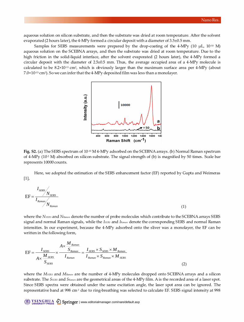
aqueous solution on silicon substrate, and then the substrate was dried at room temperature. After the solvent
evaporated (2 hours later), the 4-MPy formed a circular deposit with a diameter of 3.5±0.5 mm.
Samples for SERS measurements were prepared by the drop-coating of the 4-MPy (10 µL, 10-10 M)
aqueous solution on the SCEBNA arrays, and then the substrate was dried at room temperature. Due to the
high friction in the solid-liquid interface, after the solvent evaporated (2 hours later), the 4-MPy formed a
circular deposit with the diameter of 2.5±0.5 mm. Thus, the average occupied area of a 4-MPy molecule is
calculated to be 8.2×10⁻¹¹ cm2, which is obviously larger than the maximum surface area per 4-MPy (about
7.0×10⁻¹⁵ cm2). So we can infer that the 4-MPy deposited film was less than a monolayer.
Fig. S2. (a) The SERS spectrum of 10-10 M 4-MPy adsorbed on the SCEBNA arrays. (b) Normal Raman spectrum
of 4-MPy (10-2 M) absorbed on silicon substrate. The signal strength of (b) is magnified by 50 times. Scale bar
represents 10000 counts.
Here, we adopted the estimation of the SERS enhancement factor (EF) reported by Gupta and Weimeras
[1],
(1)
where the NSERS and NRaman denote the number of probe molecules which contribute to the SCEBNA arrays SERS
signal and normal Raman signals, while the ISERS and IRaman denote the corresponding SERS and normal Raman
intensities. In our experiment, because the 4-MPy adsorbed onto the sliver was a monolayer, the EF can be
written in the following form,
(2)
where the MSERS and MRaman are the number of 4-MPy molecules dropped onto SCEBNA arrays and a silicon
substrate. The SSERS and SRaman are the geometrical areas of the 4-MPy film. A is the recorded area of a laser spot.
Since SERS spectra were obtained under the same excitation angle, the laser spot area can be ignored. The
representative band at 998 cm-1 due to ring-breathing was selected to calculate EF. SERS signal intensity at 998
Raman
Raman
SERS
SERS
NI
NI
EF
SERSRamanRaman
RamanSERSSERS
Raman
Raman
Raman
SERS
SERS
SERS
MSI
MSI
I
S
MA
S
MA
I
EF

www.theNanoResearch.com∣www.Springer.com/journal/12274 | Nano Research
Nano Res.
cm-1 is 8400 cps and normal Raman signal intensity at 1003 cm-1 is 40 cps (see Figure S2). The SSERS and SRaman are
0.045 and 0.096 cm2. We calculated EF by using the expressions (2) and the value of EF is 9.8×10 9. EF was
calculated to be 7.4×10⁹ when ISERS at 1091 cm-1 was used.
3. Finite difference time domain (FDTD) simulation
3.1. Modeling details
Lumerical FDTD Solutions software was used to simulate the electromagnetic field intensity and spatial
distribution around SCEBNA arrays [2]. The schematic representation of our modeling strategy is shown in
Figure S3. Similar to the method of previous works [3, 4], we truncate all apexes of triangles to represent the
round tips of actually fabricated Au-Ag nanotriangles (Figure S3a). The side length of gold triangles (lAu),
truncation width of gold triangles (wAu) and silver triangles (wAg) are fixed at 130 nm, 5 nm and 10 nm,
respectively. Considering that the diameter of hexagonal closely packed PS spheres is 360 nm, the gap size (d)
depends on the length of silver triangles (lAg), which is variable. The centroids of each gold triangle and the
corresponding silver triangular coating are aligned in the z-axis direction. For simplicity, the silicon pillar that holds up the coaxial Au-Ag triangles is set as coaxial cylinders with 40 nm in diameter and 80 nm in height (hSi).
The thickness of gold (hAu) is fixed at 30 nm. On the silicon substrate, a planar silver layer is deposited, whose
thickness is equal to the thickness of silver triangle (hAg). Right below each silver triangle, an isometrical and
coaxial air truncated triangular cavity (black dashed area in Figure S3b) is located in the silver la yer to roughly
represent the void volume under the Au-Ag nano-mask during the silver deposition process. All the dielectric
properties of Au, Ag, and Si were taken from Palik’s handbook [5].
Fig. S3. (a, b) Schematic illustration of the top view and the side view of the FDTD model, respectively.
During the calculation process, we choose one unit cell of the hexagonal bowtie array in xy plane as the
simulation region, whose symcenter is located at zero point. 180 nm above this region, a sufficiently wide
source of plane wave (at 350 to 700 nm wavelength) is placed. The plane wave polarizes along the x-direction
and propagates along negative z-direction. Based on this configuration, anti-symmetric and symmetric
condition can be used at the x and y boundaries of the simulation domain to save calculation time without
losing the precision. The top and bottom boundaries are 360 nm above the silver triangle and 100 nm below the
silicon pillar, relatively, and set as perfectly matched layers. The accuracy of the conformal mesh is 8. Around
the central elevated bowtie, we also placed an override mesh with step size of 1.5 nm (dx=dy=dz). Two 2D
z-normal (at top and bottom of silver bowties, blue dashed lines in Figure S3b) and one 2D y-normal profile
monitors (across the centroids of both silver triangles, blue dashed lines in Figure S3a) are placed to record the
standard Fourier transformed electric-field intensity at 532 nm wavelength which is the excitation wavelength
in our SERS experiment.
3.2. Dependence of the field distribution on the silver thickness
We simulated the field distribution near to the SCEBNAs with different silver thicknesses and gap sizes.
The intensity contour plots are shown in Figure S4. It’s clearly seen that when hSi > hAg (mode 1), the hot spots
locate at the gaps’ bottom; but when hSi < hAg (mode 2), they locate at the gaps’ top.

| www.editorialmanager.com/nare/default.asp
Nano Res.
Fig. S4. Contour plots of electric field intensity distribution in the xz plane with different thicknesses of silver,
(a) 45, (b) 60, (c) 95, (d) 120, (e) 140, and (f) 180 nm. The corresponding gap size are (a) 44, (b) 32, (c) 28, (d) 28, (e)
25, and (f) 18 nm.
3.3. Dependence of the reflection on the gap size
We simulated the optical reflection of the SCEBNA arrays with 60- or 95-nm silver coatings under the
532-nm-wavelength incidence. Results are plotted in Figure S5. It's clearly that as increasing the gap size, the
reflection decreases gradually. This leads to a better coupling of the incident light into the surface plasmons.
Fig. S5. Simulated optical reflection under 532-nm-wavelength incidence on the SCEBNA arrays with various
gap sizes. Mode 1 and 2 stand for SCEBNA arrays with 60- and 95-nm-thick silver.

www.theNanoResearch.com∣www.Springer.com/journal/12274 | Nano Research
Nano Res.
References
[1] Xia, Y.; Rogers, J. A.; Paul, K. E.; Whitesides, G. M. Unconventional methods for fabricating and patterning nanostructures.
Chem. Rev. 1999, 99, 1823-1848.
[2] Lumerical Solutions Inc., https://www.lumerical.com/, accessed: August, 2014.
[3] Fischer Holger, M. O. J. F. Engineering the optical response of plasmonic nanoantennas. Opt. Express 2008, 16, 9144-9154.
[4] Jin Rongchao, C. Y., Mirkin Chad A., Kelly, K.L.,Schatz George C.,Zheng J.G. Photoinduced conversion of silver nanospheres to
nanoprisms. Science 2001, 294, 1901-1903.
[5] Palik, E. D. Handbook of optical constants of solids. Academic Press: Orlando, FL, 1985.