SILICON AND CARBON BASED NANOWIRES - Bilkent University · SILICON AND CARBON BASED NANOWIRES a...
99
SILICON AND CARBON BASED NANOWIRES a thesis submitted to the department of physics and the institute of engineering and science of b ˙ ilkent university in partial fulfillment of the requirements for the degree of master of science By Sefaattin TONGAY January, 2004
Transcript of SILICON AND CARBON BASED NANOWIRES - Bilkent University · SILICON AND CARBON BASED NANOWIRES a...

SILICON AND CARBON BASEDNANOWIRES
a thesis
submitted to the department of physics
and the institute of engineering and science
of bilkent university
in partial fulfillment of the requirements
for the degree of
master of science
By
Sefaattin TONGAY
January, 2004

I certify that I have read this thesis and that in my opinion it is fully adequate,
in scope and in quality, as a thesis for the degree of Master of Science.
Prof. Dr. Salim Cıracı (Advisor)
I certify that I have read this thesis and that in my opinion it is fully adequate,
in scope and in quality, as a thesis for the degree of Master of Science.
Prof. Dr. Atilla Aydınlı
I certify that I have read this thesis and that in my opinion it is fully adequate,
in scope and in quality, as a thesis for the degree of Master of Science.
Prof. Dr. Sakir Erkoc
Approved for the Institute of Engineering and Science:
Prof. Dr. Mehmet B. BarayDirector of the Institute Engineering and Science
ii

ABSTRACT
SILICON AND CARBON BASED NANOWIRES
Sefaattin TONGAY
M.S. in Physics
Supervisor: Prof. Dr. Salim Cıracı
January, 2004
Nanowires have been an active field of study since last decade. The reduced
dimensionality end size allowing electrons can propagate only in one direction has
led to quantization which are rather different from the bulk structure. As a re-
sult, nanowires having cross section in the range of Broglie wavelength have shown
stepwise electrical and thermal conductance, giant Young modulus, stepwise vari-
ation of the cross-section etc. Moreover, the atomic structure of nanowires have
exhibited interesting regularities which are not known in two or three dimensions.
These novel properties of nanowires have been actively explored since last decade
in order to find an application in the rapidly developing field of nanotechnology.
In the present thesis, we investigated the atomic and electronic structure of
a variety of Si and C atom based very thin nanowires starting from linear chain
including pentagonal, hexagonal and tubular structures. We found that the C
and Si linear chains form double bonds and have high binding energy. Although
bulk carbon in diamond structure is an insulator, carbon linear chain is metal and
has twice conductance of the gold chain. We carried out an extensive analysis
of stability and conductance of the other wires. Our study reveals that Si and
C based nanowires generally show metallic properties in spite of the fact that
they are insulator or semiconductor when they are in bulk crystal structure.
Metallicity occurs due to change in the character and order of bonds.
Keywords: ab initio, first principles, nanowires, density functional theory, nan-
otubes, conductance.
iii
OZET
SILIKON VE KARBON TABANLI NANOTELLER
Sefaattin TONGAY
Fizik , Yuksek Lisans
Tez Yoneticisi: Prof. Dr. Salim Cıracı
Ocak, 2004
Nanoteller gecen on yıldan beridir aktif bir arastırma alanidir. Indirgenmis
boyut ve buyuklugun elektronların bir yonlu hareketine izin vermesi, bulk yapıdan
oldukca farklı olarak, kesiklilige sebebiyet vermektedir. Sonuc olarak, Broglie dal-
gaboyu mertebesinde kesit alanına sahip nanoteller, basamaklı yapıda elektriksel
ve ısısal iletkenlik, yuksek Young modulu ve kesikli olarak degisen kesit alanı gibi
ozellikler gostermektedir. Dahası, nanotellerin atomik yapısı iki ve uc boyutta
bilinmeyen ilginc duzenlilige sahiptir. Nanotellerin bu belli baslı ozellikleri nan-
oteklonojinin hızla gelisen alanlarında bir uygulama bulmak amacıyla gectigimiz
on yıldan beridir aktif olarak arastırılmaktadır.
Bu tezde, silikon ve karbon icn dogrusal zincir yapıdan baslayarak, besgensel,
altıgensel ve tupsel yapıların atomik ve elektronik yapılari incelenmistir. C ve
Si dogrusal zincir yapılarında cift bag olusumu sebebiyle bu yapıların yuksek
baglanma enerjisine sahip oldukları bulunmustur. Elmas yapıdaki bulk kar-
bon yalıtkan olmakla beraber, karbon dogrusal zincir yapı metalik olup, altın
dogrusal zincir yapıya nazaran iki kat iletkenlige sahiptir. Diger tel yapılar icin
detaylı kararlılık ve iletkenlik analizleri yurutulmustur. Yapılan analizler Si ve
C temelli nanotellerin, bulk kristal yapılarının yalıtkan veya yarıiletken olmasına
ragmen, genel olarak metalik ozelliklere sahip oldugunu gostermektedir. Bu meta-
lik davranıs, bagların karekterindeki ve yonlenimindeki degisiklikten ileri gelmek-
tedir.
Anahtar sozcukler : ab initio, temel prensipler, nanoteller, durum fonksiyonu
teorisi, karbon nanotup, iletkenlik.
iv

Acknowledgement
I would like to express my deepest gratitude and respect to my supervisor Prof.
Dr. Salim Cıracı for his patience and guidance during my study including nights
and weekends and also for giving me a chance to be one his assistant. I really
feel lucky to meet him...
I am thankful to Assc. Prof. Dr. Oguz Gulseren and Dr. Tugrul Senger for
his valuable discussions and advices.
I appreciate Prof. Dr. Atilla Aydınlı for his motivation. I’m very glad to be
one his assistant in freshmen physics course for three semesters.
I also remember Prof. Dr. Huseyin Erbil, Prof. Dr. Nizamettin Armagan
whose discussions and thoughts have always motivated me and give very valuable
physical interpretation, my senior project advisor Prof. Dr. Emine Cebe and
Prof. Dr. Fevzi Buyukkilinc for the days I spent in Ege University theoretical
physics department.
My sincere thanks due to Dr. Ceyhun Bulutay for his motivation and guidance
but especially for the human profile he draws which I imagine to be like one in
future.
I would like to thank to my companion, my home-mate and my office-mate
Yavuz Ozturk for being my closest friend. Simply, thanks for everything...
I would never forget my ’brother’ Altan Cakır, from the precious undergrad-
uate days. I’m expecting great collaboration between us in the near future. In
your speech ”My brother!”
I would never forget the help and motivation of Engin Durgun, Sefa Dag,
Deniz Cakir, Cem Sevik, Ayhan Yurtsever and my home-mates Nezih Turkcu,
Cem Kuscu, Faik Demirors and Anıl Agıral.
v

vi
I would like to thank to all my friends in Physics Department for their friend-
ship.
I am thankful to the all the members of ”Ataturkcu Dusunce Dernegi” both
in Izmir and Ankara.
I would like to thank to Funda Guney for her moral support in my hard times
and endless love... Thank you for everything!..
I bless to my mother Suzan Tongay, my father Ergun Tongay for their end-
less love and support. I would like to thank to my sister Nazan Gezek, Pervin
Villasenor Ville, my brother Mehmet Ali Aydın, and Ahmet Gezek, Dilek Aydın,
Selim Gezek, Altay Gezek, Mert Aydın. But someone that I never forget their
names are: Erol Ucer and Aysel Ucer. Thanks for everything. Thanks for be-
ing my close relatives. Thanks for supporting me starting from my high school
education to graduate study both financially and morally. I’m really very happy
to be one of the member of my family. And all of my success in past, previous
and future is not mine but all of these people that I have mentioned and cannot
mentioned...
Contents
1 Introduction 1
2 Nanowires 8
2.1 Different types of nanowires . . . . . . . . . . . . . . . . . . . . . 8
2.1.1 Single Nanowires . . . . . . . . . . . . . . . . . . . . . . . 8
2.1.2 Single Wall Carbon Nanotubes (SWNTs) . . . . . . . . . . 9
2.1.3 Functionalized SWNTs . . . . . . . . . . . . . . . . . . . . 12
2.1.4 Coated Carbon Nanotubes . . . . . . . . . . . . . . . . . . 12
2.2 Physical Properties of Nanowires . . . . . . . . . . . . . . . . . . 13
2.2.1 Electronic Structure . . . . . . . . . . . . . . . . . . . . . 13
2.2.2 Quantum Conductance . . . . . . . . . . . . . . . . . . . . 13
2.2.3 Thermal Conductance . . . . . . . . . . . . . . . . . . . . 16
3 Theoretical Background 18
3.1 Born-Oppenheimer Approximation . . . . . . . . . . . . . . . . . 18
3.2 The Electronic Problem . . . . . . . . . . . . . . . . . . . . . . . 19
vii
CONTENTS viii
3.3 Density Functional Theory . . . . . . . . . . . . . . . . . . . . . . 21
3.3.1 Hohenberg-Kohn Formulation . . . . . . . . . . . . . . . . 23
3.3.2 Kohn-Sham Equations . . . . . . . . . . . . . . . . . . . . 24
3.4 Exchange and Correlation . . . . . . . . . . . . . . . . . . . . . . 25
3.4.1 Local Density Approximation (LDA) . . . . . . . . . . . . 27
3.4.2 Generalized Gradient Approximation (GGA) . . . . . . . . 28
3.5 Other Details of Calculations . . . . . . . . . . . . . . . . . . . . 29
3.6 Calculation of Conductance Based on Empirical Tight-Binding
Method . . . . . . . . . . . . . . . . . . . . . . . . . . . . . . . . 33
3.6.1 Green’s Function Method . . . . . . . . . . . . . . . . . . 33
3.6.2 Empirical Tight-Binding Method (ETB) . . . . . . . . . . 34
4 Results and Discussion 36
4.1 Motivation . . . . . . . . . . . . . . . . . . . . . . . . . . . . . . . 36
4.2 Method of calculations . . . . . . . . . . . . . . . . . . . . . . . . 37
4.3 Carbon and Silicon Nanowires . . . . . . . . . . . . . . . . . . . . 37
4.3.1 Linear Chain C1 and Si1 . . . . . . . . . . . . . . . . . . . 37
4.3.2 Planar Triangular (C2 and Si2) . . . . . . . . . . . . . . . 45
4.3.3 Zigzag Structure (C3 and Si3) . . . . . . . . . . . . . . . . 47
4.3.4 Dumbell Structure (C4 and Si4) . . . . . . . . . . . . . . . 48
4.3.5 Triangular Structure (CT1, CT2 and SiT1, SiT2) . . . . . . 51

CONTENTS ix
4.3.6 Triangular Structure with Linear Chain . . . . . . . . . . . 53
4.3.7 Triangle+Single Atom+Single Atom (CT5) . . . . . . . . . 54
4.3.8 Pentagonal structures . . . . . . . . . . . . . . . . . . . . . 56
4.3.9 Pentagonal Structures with Linear Chain . . . . . . . . . . 59
4.3.10 Hexagonal Structures . . . . . . . . . . . . . . . . . . . . . 60
4.3.11 Hexagonal Structures with Linear Chain . . . . . . . . . . 63
4.3.12 Hexagon+Hexagon+Triangle Structure (CH5 and SiH5) . . 64
4.3.13 Buckled Hexagon and Triangle Based Structure(CH6 and
SiH6) . . . . . . . . . . . . . . . . . . . . . . . . . . . . . . 66
4.3.14 Silicon Nanotubes . . . . . . . . . . . . . . . . . . . . . . . 68
4.4 Conclusions and Future Work . . . . . . . . . . . . . . . . . . . . 73
4.4.1 Conclusions . . . . . . . . . . . . . . . . . . . . . . . . . . 73
4.4.2 Future Work . . . . . . . . . . . . . . . . . . . . . . . . . . 74
4.4.3 General Remarks . . . . . . . . . . . . . . . . . . . . . . . 75
List of Figures
2.1 Representation single wall carbon nanotubes by rolling up the
graphene layer. . . . . . . . . . . . . . . . . . . . . . . . . . . . . 9
2.2 Carbon nanotube is a single layer of graphite rolled into a cylinder. 10
2.3 A (5,5) armchair nanotube (top), a (9,0) zigzag nanotube (middle)
and a (10,5) chiral nanotube. . . . . . . . . . . . . . . . . . . . . 11
2.4 Conductance G at room temperature measured as a function of
depth of immersion of the nanotube bundle into the liquid gal-
lium. As the nanotube bundle is dipped into the liquid metal,
the conductance increases in steps of G0=2e2/h. The steps corre-
sponds to different nanotubes coming successively into the contact
with the liquid. [11] . . . . . . . . . . . . . . . . . . . . . . . . . . 14
3.1 Schematic representation of Local Density Approximation . . . . 27
3.2 Summary of the electron-electron interactions where the coulom-
bic interactions excluded. (a) the Hartree approximation, (b) the
Hartree-Fock approximation, (c) the local density approximation
and (d) the local spin density approximation which allows for dif-
ferent interactions for like-unlike spins. . . . . . . . . . . . . . . . 29
3.3 Supercell geometry for a molecule. Supercell is chosen large enough
to prevent interactions between the nearest neighbor molecules. . 31
x

LIST OF FIGURES xi
3.4 Schematic diagram of the relationship between all electron and
pseudo potentials, and wavefunctions (Reproduced from University
Basel Nanoscience web-page). . . . . . . . . . . . . . . . . . . . . 32
3.5 A conductor described by the Hamiltonian HC , connected to leads
L and R, through the coupling matrices hLC and hCR . . . . . . . 33
4.1 Energy versus number of k-points graph for carbon. . . . . . . . . 38
4.2 Energy versus energy cutoff value graph for carbon. . . . . . . . . 39
4.3 Relaxed structure of C1 and Si1 in double unit cell with lattice
parameters as = bs = 10 A, cs = 2 · 1.269 A and binding energy
Ebinding = 8.29 eV/atom for relaxed C1 structure, and as=bs=10
A, c = 2·2.217A, Ebinding = 3.45 eV/atom for Si1 relaxed structure.
Supercell is defined by lateral black lines. . . . . . . . . . . . . . . 39
4.4 Energy band structure of carbon linear chain C1. The Fermi level
(EF ) is set at the zero conventionally in this thesis and is shown
by dashed dotted line. . . . . . . . . . . . . . . . . . . . . . . . . 40
4.5 Energy band structure of optimized silicon linear chain (Si1).
Dashed dotted line corresponds to Fermi level (EF ) set at 0 eV. . 41
4.6 Density of states (DOS) of carbon linear chain described in Fig. 4.3.
Dashed dotted lines corresponds to Fermi level EF set at 0 eV. The
claim is metallic owing to the finite DOS at EF . . . . . . . . . . . 42
4.7 Density of states of Silicon linear chain (Si1) described in Fig. 4.3.
Dashed dotted lines corresponds to Fermi level EF set at 0 eV.
Since there is finite density of states at EF , Si1 structure is metallic. 42
LIST OF FIGURES xii
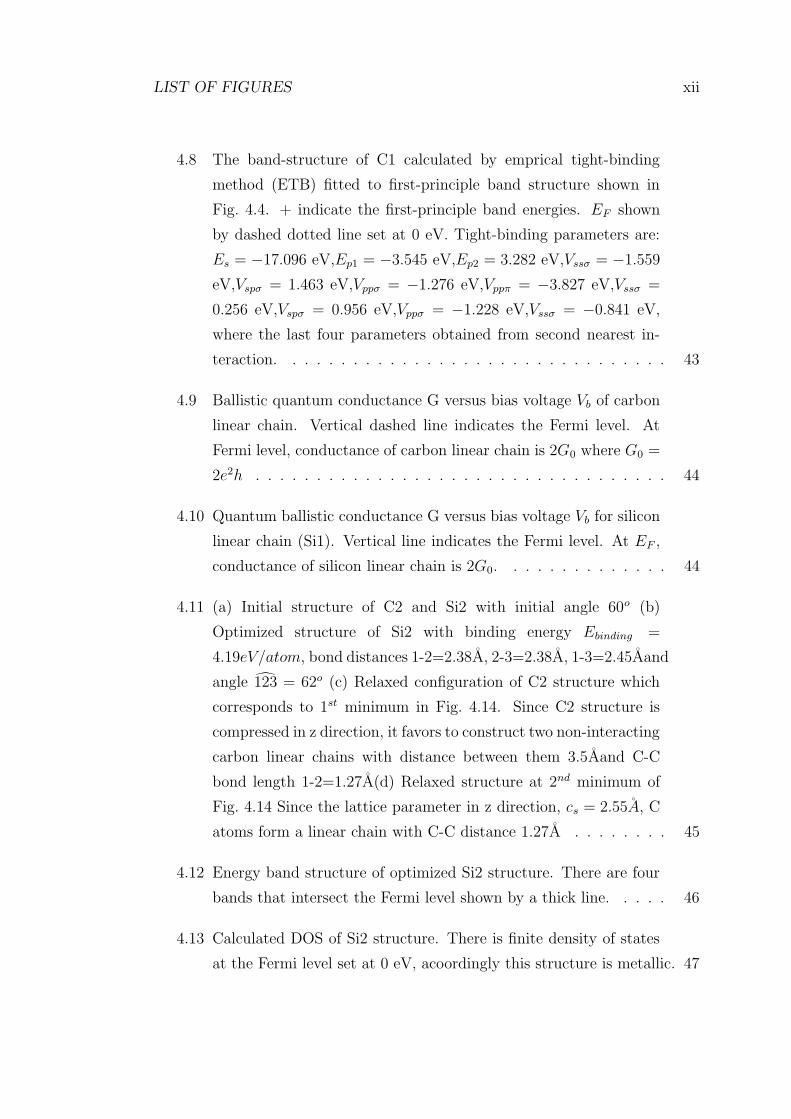
4.8 The band-structure of C1 calculated by emprical tight-binding
method (ETB) fitted to first-principle band structure shown in
Fig. 4.4. + indicate the first-principle band energies. EF shown
by dashed dotted line set at 0 eV. Tight-binding parameters are:
Es = −17.096 eV,Ep1 = −3.545 eV,Ep2 = 3.282 eV,Vssσ = −1.559
eV,Vspσ = 1.463 eV,Vppσ = −1.276 eV,Vppπ = −3.827 eV,Vssσ =
0.256 eV,Vspσ = 0.956 eV,Vppσ = −1.228 eV,Vssσ = −0.841 eV,
where the last four parameters obtained from second nearest in-
teraction. . . . . . . . . . . . . . . . . . . . . . . . . . . . . . . . 43
4.9 Ballistic quantum conductance G versus bias voltage Vb of carbon
linear chain. Vertical dashed line indicates the Fermi level. At
Fermi level, conductance of carbon linear chain is 2G0 where G0 =
2e2h . . . . . . . . . . . . . . . . . . . . . . . . . . . . . . . . . . 44
4.10 Quantum ballistic conductance G versus bias voltage Vb for silicon
linear chain (Si1). Vertical line indicates the Fermi level. At EF ,
conductance of silicon linear chain is 2G0. . . . . . . . . . . . . . 44
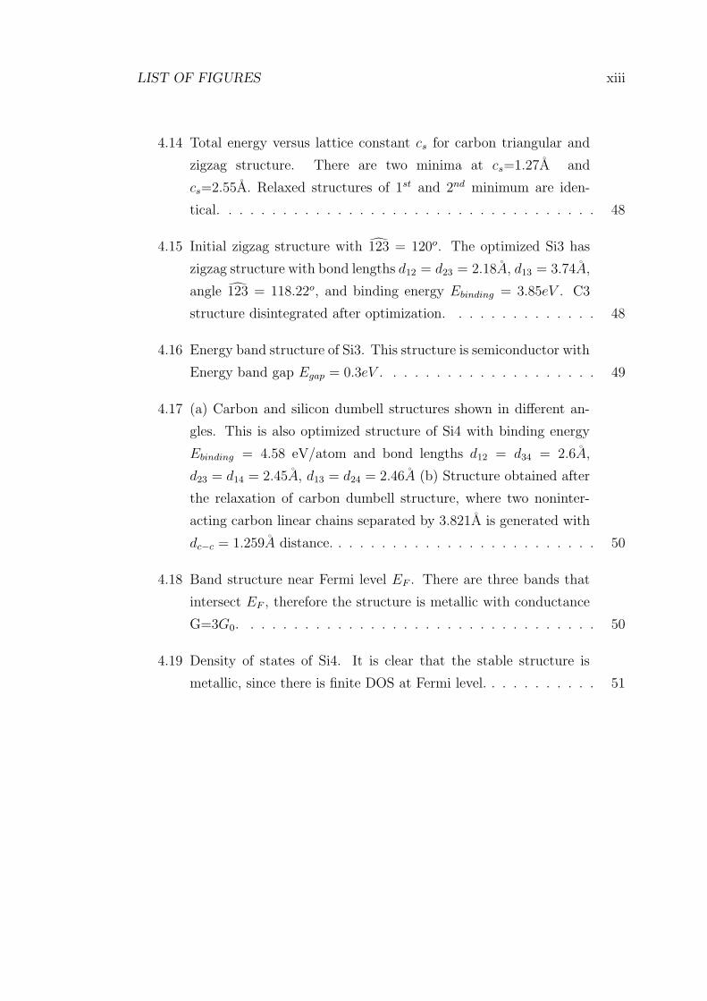
4.11 (a) Initial structure of C2 and Si2 with initial angle 60o (b)
Optimized structure of Si2 with binding energy Ebinding =
4.19eV/atom, bond distances 1-2=2.38A, 2-3=2.38A, 1-3=2.45Aand
angle 123 = 62o (c) Relaxed configuration of C2 structure which
corresponds to 1st minimum in Fig. 4.14. Since C2 structure is
compressed in z direction, it favors to construct two non-interacting
carbon linear chains with distance between them 3.5Aand C-C
bond length 1-2=1.27A(d) Relaxed structure at 2nd minimum of
Fig. 4.14 Since the lattice parameter in z direction, cs = 2.55A, C
atoms form a linear chain with C-C distance 1.27A . . . . . . . . 45
4.12 Energy band structure of optimized Si2 structure. There are four
bands that intersect the Fermi level shown by a thick line. . . . . 46
4.13 Calculated DOS of Si2 structure. There is finite density of states
at the Fermi level set at 0 eV, acoordingly this structure is metallic. 47
LIST OF FIGURES xiii
4.14 Total energy versus lattice constant cs for carbon triangular and
zigzag structure. There are two minima at cs=1.27A and
cs=2.55A. Relaxed structures of 1st and 2nd minimum are iden-
tical. . . . . . . . . . . . . . . . . . . . . . . . . . . . . . . . . . . 48
4.15 Initial zigzag structure with 123 = 120o. The optimized Si3 has
zigzag structure with bond lengths d12 = d23 = 2.18A, d13 = 3.74A,
angle 123 = 118.22o, and binding energy Ebinding = 3.85eV . C3
structure disintegrated after optimization. . . . . . . . . . . . . . 48
4.16 Energy band structure of Si3. This structure is semiconductor with
Energy band gap Egap = 0.3eV . . . . . . . . . . . . . . . . . . . . 49
4.17 (a) Carbon and silicon dumbell structures shown in different an-
gles. This is also optimized structure of Si4 with binding energy
Ebinding = 4.58 eV/atom and bond lengths d12 = d34 = 2.6A,
d23 = d14 = 2.45A, d13 = d24 = 2.46A (b) Structure obtained after
the relaxation of carbon dumbell structure, where two noninter-
acting carbon linear chains separated by 3.821A is generated with
dc−c = 1.259A distance. . . . . . . . . . . . . . . . . . . . . . . . . 50
4.18 Band structure near Fermi level EF . There are three bands that
intersect EF , therefore the structure is metallic with conductance
G=3G0. . . . . . . . . . . . . . . . . . . . . . . . . . . . . . . . . 50
4.19 Density of states of Si4. It is clear that the stable structure is
metallic, since there is finite DOS at Fermi level. . . . . . . . . . . 51
LIST OF FIGURES xiv
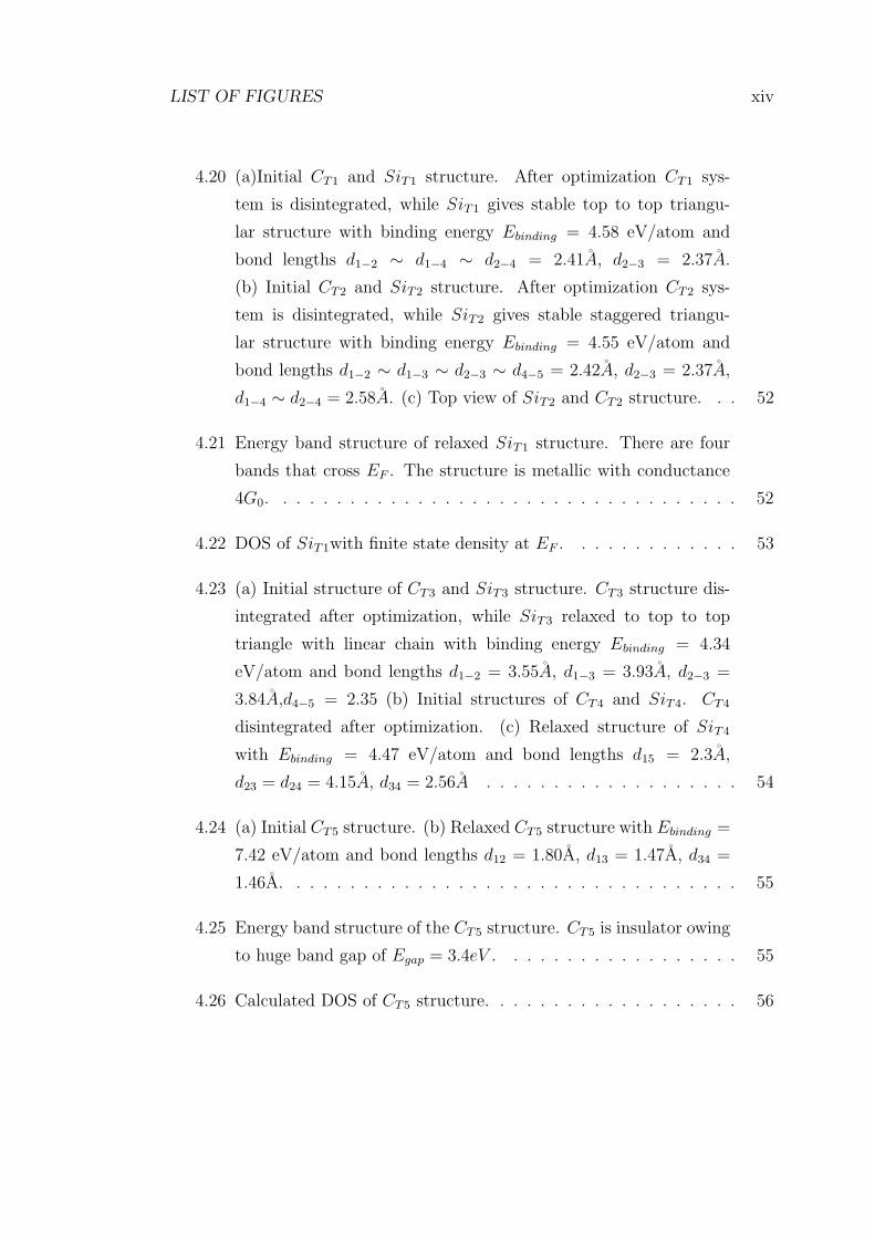
4.20 (a)Initial CT1 and SiT1 structure. After optimization CT1 sys-
tem is disintegrated, while SiT1 gives stable top to top triangu-
lar structure with binding energy Ebinding = 4.58 eV/atom and
bond lengths d1−2 ∼ d1−4 ∼ d2−4 = 2.41A, d2−3 = 2.37A.
(b) Initial CT2 and SiT2 structure. After optimization CT2 sys-
tem is disintegrated, while SiT2 gives stable staggered triangu-
lar structure with binding energy Ebinding = 4.55 eV/atom and
bond lengths d1−2 ∼ d1−3 ∼ d2−3 ∼ d4−5 = 2.42A, d2−3 = 2.37A,
d1−4 ∼ d2−4 = 2.58A. (c) Top view of SiT2 and CT2 structure. . . 52
4.21 Energy band structure of relaxed SiT1 structure. There are four
bands that cross EF . The structure is metallic with conductance
4G0. . . . . . . . . . . . . . . . . . . . . . . . . . . . . . . . . . . 52
4.22 DOS of SiT1with finite state density at EF . . . . . . . . . . . . . 53
4.23 (a) Initial structure of CT3 and SiT3 structure. CT3 structure dis-
integrated after optimization, while SiT3 relaxed to top to top
triangle with linear chain with binding energy Ebinding = 4.34
eV/atom and bond lengths d1−2 = 3.55A, d1−3 = 3.93A, d2−3 =
3.84A,d4−5 = 2.35 (b) Initial structures of CT4 and SiT4. CT4
disintegrated after optimization. (c) Relaxed structure of SiT4
with Ebinding = 4.47 eV/atom and bond lengths d15 = 2.3A,
d23 = d24 = 4.15A, d34 = 2.56A . . . . . . . . . . . . . . . . . . . 54
4.24 (a) Initial CT5 structure. (b) Relaxed CT5 structure with Ebinding =
7.42 eV/atom and bond lengths d12 = 1.80A, d13 = 1.47A, d34 =
1.46A. . . . . . . . . . . . . . . . . . . . . . . . . . . . . . . . . . 55
4.25 Energy band structure of the CT5 structure. CT5 is insulator owing
to huge band gap of Egap = 3.4eV . . . . . . . . . . . . . . . . . . 55
4.26 Calculated DOS of CT5 structure. . . . . . . . . . . . . . . . . . . 56
LIST OF FIGURES xv
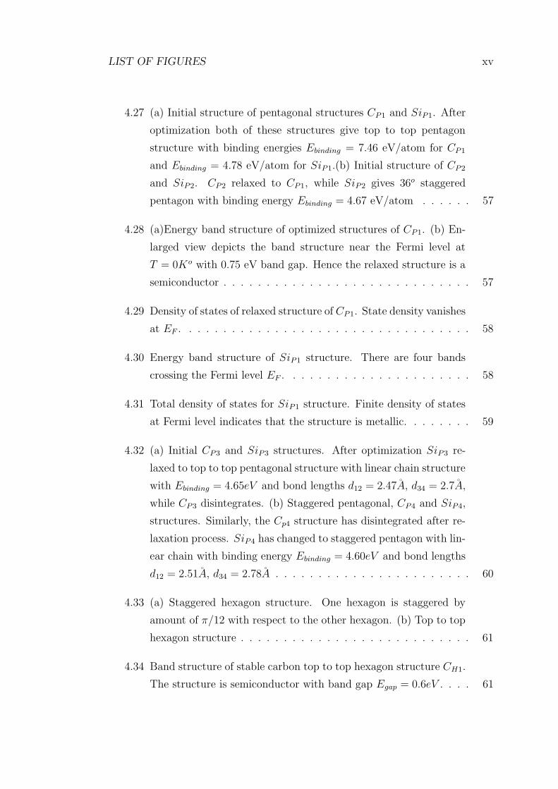
4.27 (a) Initial structure of pentagonal structures CP1 and SiP1. After
optimization both of these structures give top to top pentagon
structure with binding energies Ebinding = 7.46 eV/atom for CP1
and Ebinding = 4.78 eV/atom for SiP1.(b) Initial structure of CP2
and SiP2. CP2 relaxed to CP1, while SiP2 gives 36o staggered
pentagon with binding energy Ebinding = 4.67 eV/atom . . . . . . 57
4.28 (a)Energy band structure of optimized structures of CP1. (b) En-
larged view depicts the band structure near the Fermi level at
T = 0Ko with 0.75 eV band gap. Hence the relaxed structure is a
semiconductor . . . . . . . . . . . . . . . . . . . . . . . . . . . . . 57
4.29 Density of states of relaxed structure of CP1. State density vanishes
at EF . . . . . . . . . . . . . . . . . . . . . . . . . . . . . . . . . . 58
4.30 Energy band structure of SiP1 structure. There are four bands
crossing the Fermi level EF . . . . . . . . . . . . . . . . . . . . . . 58
4.31 Total density of states for SiP1 structure. Finite density of states
at Fermi level indicates that the structure is metallic. . . . . . . . 59
4.32 (a) Initial CP3 and SiP3 structures. After optimization SiP3 re-
laxed to top to top pentagonal structure with linear chain structure
with Ebinding = 4.65eV and bond lengths d12 = 2.47A, d34 = 2.7A,
while CP3 disintegrates. (b) Staggered pentagonal, CP4 and SiP4,
structures. Similarly, the Cp4 structure has disintegrated after re-
laxation process. SiP4 has changed to staggered pentagon with lin-
ear chain with binding energy Ebinding = 4.60eV and bond lengths
d12 = 2.51A, d34 = 2.78A . . . . . . . . . . . . . . . . . . . . . . . 60
4.33 (a) Staggered hexagon structure. One hexagon is staggered by
amount of π/12 with respect to the other hexagon. (b) Top to top
hexagon structure . . . . . . . . . . . . . . . . . . . . . . . . . . . 61
4.34 Band structure of stable carbon top to top hexagon structure CH1.
The structure is semiconductor with band gap Egap = 0.6eV . . . . 61
LIST OF FIGURES xvi
4.35 Calculated total density of states of CH1. . . . . . . . . . . . . . . 62
4.36 Energy band structure of SiH1 structure.There are four bands in-
tersecting the Fermi level represented by dashed lines. . . . . . . . 62
4.37 Calculated density of states (DOS) of SiH1. . . . . . . . . . . . . 63
4.38 (a) Staggered hexagon with linear chain structure where one
hexagon is rotated in its plane by an angle φ = 30o relative to
the adjacent hexagons. (b) Top to top hexagon with linear chain
structure. . . . . . . . . . . . . . . . . . . . . . . . . . . . . . . . 64
4.39 (a) Initial CH5 and SiH5 structures. This structure consists of two
buckled hexagons and one triangle (b) The optimized structure
of CH5 with Ebinding = 7.99eV and bond lengths d12 = 1.35A,
d23 = 1.51A, d34 = 1.33A. This structure is similar to the initial
one, except that the bond lengths between the atoms of triangular
layer are now stretched. . . . . . . . . . . . . . . . . . . . . . . . 65
4.40 (a) Energy band structure of stable CH5 structure. There is one
two-fold degenerate band which intersects the Fermi level. There-
fore the structure is metallic with conductance 2G0. . . . . . . . . 65
4.41 Calculated DOS of CH5 . . . . . . . . . . . . . . . . . . . . . . . 66
4.42 (a) Initial triangle+hexagon+staggered triangle+hexagon struc-
ture (CH6 and SiH6). (b) The optimized structure of CH6 with
Ebinding = 7.93eV and bond lengths d12 = 1.319A, d23 = 1.319A,
d34 = 1.52A, d45 = 1.315A. . . . . . . . . . . . . . . . . . . . . . . 67
4.43 (a) Energy band structure of stable CH6 structure. There are
roughly 3 bands that intersect Fermi level. . . . . . . . . . . . . . 67
4.44 Calculated DOS of stable CH6 structure. . . . . . . . . . . . . . . 68
LIST OF FIGURES xvii
4.45 Silicon (8,0) tube in a supercell with lattice parameters as = bs =
20 Aand cs = 6 A. After optimization (8,0) tube relaxed to (8,0)
tube with c=6.67Aand binding energy Ebinding = 4.80 eV/atom. . 69
4.46 Energy band structure of silicon (8,0) tube. There are three bands
intersecting the Fermi level. . . . . . . . . . . . . . . . . . . . . . 69
4.47 Calculated DOS of the silicon zigzag (8,0) SWNT. There is finite
density of states at Fermi level represented by dashed dotted lines. 70
4.48 Relaxed structure of armchair silicon (3,3) nanotube. with
c=3.82Aand binding energy Ebinding = 4.7 eV/atom. . . . . . . . . 71
4.49 Calculated band structure of Si (3,3) nanotube. Two bands inter-
secting the EF attribute metallic charecter to the structure. . . . 72
4.50 Calculated density of states of (3,3) armchair Si nanotube. . . . . 72
4.51 The variation of interaction energy of C in bcc, fcc and diamond
structures obtained by using GGA. These structures have bind-
ing energies, Ebccbinding=-2 eV/atom, Efccbinding=-3.3 eV/atom and
Ediamondbinding=-8.43 eV/atom. . . . . . . . . . . . . . . . . . . . . 76
4.52 The variation of interaction energy of C in bcc, fcc and diamond
structures with binding energies, Ebccbinding = −2.64 eV/atom,
Efccbinding = −3.97 eV/atom and Ediamondbinding = −9.45 eV/atom
obtained by using LDA. . . . . . . . . . . . . . . . . . . . . . . . 77

List of Tables
xviii

Chapter 1
Introduction
Importance of nanotechnology was first pointed out by Richard Feynman as early
as in 1959. In his now famous lecture entitled , ”There is Plenty of Room at the
Bottom.”, he stimulated his audience with the vision of exciting future discoveries
if one could fabricate materials and devices at the atomic/molecular scale. He
pointed out that, for this to happen, a new class of miniaturized instrumentation
would be needed to manipulate and measure the properties of these small-”nano”-
structures. But at that time, it was not possible for researchers to manipulate
single atoms or molecules because they were far too small to be dedected by the
existing tools. Thus, his speech was completely theoretical, but fantastic. He
described how the laws of physics do not limit our ability to manipulate single
atoms and molecules. Instead, it was our lack of the appropriate methods for
doing so. However, he correctly predicted that the time would come in which
atomically precise manipulation of matter would inevitably arrive.
It was not until the 1980s that instruments were invented with the capabilities
Feynman envisioned. These instruments, including scanning tunnelling micro-
scopes, atomic force microscopes, and near-field microscopes, provide the ”eyes”
and ”fingers” required for nanoscale measurements and atomic manipulations.
In a parallel development, expansion of computational capability now enables
sophisticated simulations of material behavior at the nanoscale. These new tools
and techniques have sparked excitement throughout the scientific community.
1

CHAPTER 1. INTRODUCTION 2
Traditional models and theories for material properties and device operations
involve assumptions based on ”critical length scales” which are generally larger
than several nanometers. When at least one dimension of a material structure is
under the critical length, distinct behavior often emerges that cannot be explained
by traditional or classical models and theories. Thus, scientists from many dis-
ciplines are avidly fabricating and analyzing nanostructures for the advancement
of nanoscience and nanotechnology.
Nowadays science society defines nanotechnology as the ability to work at
the molecular level, atom by atom, to create large structures with fundamen-
tally new molecular organization. Compared to the behavior of bulk materials,
nanostructures in the range of about 10−9 to 10−7 m (1 to 100 nm - a typical
dimension of 10 nm is 1,000 times smaller than the diameter of a human hair)
exhibit important changes. Nanotechnology is concerned with materials and sys-
tems whose structures and components exhibit novel and significantly improved
physical, chemical, and biological properties, phenomena, and processes due to
their nanoscale size. The aim is to exploit these properties by gaining control
of structures and devices at atomic, molecular, and supramolecular scale and
to learn how to efficiently manufacture these devices. Maintaining the stability
of interfaces and the integration of these ”nanostructures” at the micron-length
scale and macroscopic scale is another objective
New behavior at the nanoscale is not necessarily predictable from that ob-
served at large size scales. The most important changes in behavior are caused
not by the order of magnitude size reduction, but by newly observed phenomena
intrinsic to or becoming predominant at the nanoscale, such as size confinement,
predominance of interfacial phenomena and quantum mechanics. Once it is pos-
sible to control feature size, it is also possible to enhance material properties
and device functions beyond those that we currently know or even consider as
feasible. Reducing the dimensions of structures leads to entities, such as car-
bon nanotubes, nanowires and quantum dots, DNA-based structures, and laser
emitters, which have unique properties. Such new forms of materials and devices
herald a revolutionary age for science and technology, provided we can discover
and fully utilize the underlying principles.
CHAPTER 1. INTRODUCTION 3
Materials and Manufacturing. Nanotechnology is fundamentally changing the
way materials and devices will be produced in the future. The ability to synthesize
nanoscale building blocks with precisely controlled size and composition and then
to assemble them into larger structures with unique properties and functions will
revolutionize segments of the materials manufacturing industry. At present we
perceive only the tip of the iceberg in terms of the benefits that nano structuring
can bring: lighter, stronger, and programmable materials; reductions in life-cycle
costs through lower failure rates; innovative devices based on new principles and
architectures; and use of molecular/cluster manufacturing, which takes advantage
of assembly at the nanoscale level for a given purpose. We will be able to develop
structures not previously observed in nature. Challenges include synthesis of
materials by design, development of bio- and bio-inspired materials, development
of cost-effective and scalable production techniques, and determination of the
nanoscale initiators of materials failure.
Nanoelectronics and Computer Technology. Within ten years of the funda-
mental discovery of the new phenomenon of giant magnetoresistance, this nan-
otechnology completely replaced older technologies for computer disk heads and
opened new market worth $34 billion in 1998. Other potential breakthroughs
include (a) nanostructured microprocessor devices which continue the trend in
lower energy use and cost per gate, thereby improving the efficacy of computers
by a factor of millions; (b) communications systems with higher transmission fre-
quencies and more efficient utilization of the optical spectrum to provide at least
ten times more bandwidth, with consequences in business, education, entertain-
ment, and defense; (c) small mass storage devices with capacities at multi-terabit
levels, one thousand times better than today; and (d) integrated nanosensor sys-
tems capable of collecting, processing, and communicating massive amounts of
data with minimal size, weight, and power consumption. Potential applications of
nanoelectronics also include affordable virtual reality stations that provide indi-
vidualized teaching aids (and entertainment); computational capability sufficient
to enable unmanned combat and civilian vehicles; and communication capability
that obviates much commuting and other business travel in an era of increasingly
expensive transport fuels.
CHAPTER 1. INTRODUCTION 4
In the last decade, there has been a great interest in both geometrical, me-
chanical, electrical properties of nanowires and their fabrication. Nanowires are
most important structures of nanoscience and nanotechnology since they have
great potential in applied fields such as nanoelectronics as well as their very in-
teresting nature. It’s well known that the electrical and mechanical properties
of any metal are not so different, whether its size is in millimeters or in meters.
But, as soon as its size approaches the atomic size all common knowledge about
the fundamental properties of these metals becomes invalid. For example, in
Ohm’s law, the electrical resistance of any metal is proportional to its length.
However, since the distance an electron travels between two scattering events is
typically much larger than the atomic size, this fundamental law breaks down.
The electrons transverse the atomic sized conductor ballistically, and resistance
becomes independent of its length. In fact, the character of the resistance changes
conceptually and it will be necessary to invoke the wave nature of the electrons
in the conductor for a proper description. The energy scales involved are much
larger than that of the quantum effects become visible at room temperature. The
chemical nature of the metals starts to play an essential role while the size gets
smaller. As a result, while in macroscopic world any metal, say gold, with re-
spect to the other metal,say lead, is better conductor, in nanoscaled dimensions
this time lead is better than that of gold. Metal nanowires also exhibits very
interesting quantum behavior, such as quantum of conductance, even at room
temperature due to large energy level separation of the transport channels unlike
in semiconductors. In addition to unusual electronic properties the mechanical
properties by themselves are also quite unusual: plastic deformation in a macro-
scopic metal occur via structural dislocation motion. On the other hand, atomic
sized metal wires flows in response to applied stresses via structural rearrange-
ments and their yield strength is one or two orders of magnitude larger than for
bulk materials.
The experimental investigation of these phenomena requires tools for manip-
ulation and characterization of structure at the atomic and molecular scale. An
important tools that make the fabrication of such nanowires possible are Scan-
ning Tunnelling Microscope (STM) (which was developed by Gerd Binnig and
CHAPTER 1. INTRODUCTION 5
Heinrich Rohrer, for which they were awarded the nobel price in 1986) and High
Resolution Electron Microscope (HRTEM) and Mechanical Controllable Break
Junction (MCJB). One of the most important milestones in nanoscience is the
fabrication of the stable gold monatomic chains suspended between two elec-
trodes. Ohnishi et al [1], visualized these single atomic chains the first time by
transmission electron microscopy (TEM). Concomitantly Yanson et al. [2] has
produced four or five gold monatomic chain by using STM and MCJB, provided
indirect evidence for their existence.
After having pioneered the idea of molecular electronics, where individual
molecules plays the role of simple electronic device such as diod, transistor, tun-
nelling device, it is pointed out that the real challenge is in connecting these
devices. In fact, the interconnects between molecular devices have crucial device
elements as the device sizes have reduced at few nanometers.
Nanoelectronics has imposed the fabrication of stable and reproducible inter-
connects with the high conductivity with diameters smaller than that of the device
that they are connected to. Nanowires have been produced first to investigate
the coherent electron transport as fallow up of Gimzewski and Moller’s experi-
ment. Very thin metal wires and atomic chains have been produced by refracting
the STM tip from an indentation and then by thinning the neck of materials
that wets the tip. While these nanowires produced so far have played crucial
role in understanding the quantum effects in electronic and thermal conductance
they were neither stable nor reproducible to offer any relevant application. Re-
cent research has shown that armchair nanotubes and nanowires, or metal coated
carbon nanotubes can be served for this purpose and hence they make high con-
ducting, nanometersize wires to connect these devices. Apart from being used
as interconnects, nanowires have important aspects which attract the interest of
researches.
If the atoms forming a wire have net magnetic moment, and also the wire
itself have magnetic ground state, such a nanowire may offer applications as
nanomagnets. This is expected to be an emerging field for data storage and
electromagnetic devices.

CHAPTER 1. INTRODUCTION 6
In metallic electron densities, when the diameter of a wire becomes in the
range of Broglie wave lenght (ie. D ∼ λB ) the energy level spacing of electronic
and phononic states transversely confined to these wires become significant. Ow-
ing to that large level spacing, the quantized nature of electrons and phonons
continue to be observable even at room temperature. As a result the electrical
conductance G and heat conductance K exhibit quantized nature. The variation
of G itself is clearly related with the atomic structure of the wire.
The structure of nanowires itself is important. The stability and periodicity
of the atomic structure in one dimension (1D) is of academical and technologi-
cal interest, because of our limited knowledge in crystallography in one dimen-
sion. Besides, earlier research have argued that at D ∼ λB, the conductance G
(even the diameter D or size) of nanowires are quantized. In this respect, we
remind the reader from magic numbers of Si atom making silicon nanoclusters.
Group IV elements, Carbon and Silicon, make semiconductor or insulator in di-
amond structure, because of their even number of valence electrons appropriate
for tetrahedrally directed covalent bonds. Our interest in this thesis is to find
their electronic properties when they form very thin nanowires.
In this thesis, we have studied the physical properties of carbon and silicon
nanowires in detail. These two elements give many different stable nanowire
structures which can be used as an interconnect between the nanodevices. In this
thesis, various nanowires starting from carbon and silicon linear chain structure
to more complex wires and their physical properties have been extensively dis-
cussed in chapter 4. Since tubes are another class of structure for one-dimensional
nanowires, we focussed on the tubular structures of silicon. In the past decade sev-
eral novel properties of carbon nanotubes have been investigated actively. These
properties have been used to make prototypes of various electronic devices at
nanoscale. In this thesis, we will not involve with the physical properties of car-
bon nanotubes. On the other hand, Si being in the same IV column as C atom,
has similar structure and it is of intent to know whether Si has stable tubular
structure. This way, additional tubular structures such as silicon (8,0) and (3,3)
nanotubes also studied in detail. Calculated energy-band structure and density of
states of these tubular structures attribute metallic properties to them. Although

CHAPTER 1. INTRODUCTION 7
Generalized Gradient Approximation (GGA) method gives stable structure, we
applied stability test to the structure. Stability test can be applied in various ways
as discussed in Chapter 4.3.1. In our work, we chose to deform the structures and
then look for the relaxed positions of the atoms. In the second part, conduction
of C1 and Si1 is calculated by Empirical Tight-Binding Method (ETBM). This
method is discussed in Chapter 3 and Chapter 4.3.1.
This thesis is organized as follows: Chapter 2 gives a brief information about
the physical properties of different types of nanowires. Chapter 3 summarizes
the theoretical background, method of calculation and approximation methods,
Chapter 4, presents results and discussion. This work ends by giving concluding
remarks and suggestion for possible future work.

Chapter 2
Nanowires
2.1 Different types of nanowires
In the previous chapter we present an introductory explanation on the importance
and fabrication of nanowires. In this chapter we will discuss different types of
nanowires and their physical properties.
2.1.1 Single Nanowires
Nanowires have been produced by retracting the STM tip from nano indentation.
The atoms of the sample, which wet the tip have formed a neck between the tip
and sample. Metal wires having lengths as long as ∼ 400A0 were produced.
However, the prime drawback in those wires produced by STM were irregulari-
ties in their structure. Since their size and structure were not controllable and
not reproducible, serious technological applications involving those wires are not
possible.
Earlier studies based on classical molecular dynamics calculations have shown
that single atom nanowires can form. This finding confirmed experimentally by
Ohnishi et al [1] and Yanson et al [2], who fabricated stable single atom chain
8
CHAPTER 2. NANOWIRES 9
of Au between two electrodes. Later, first principle calculations demonstrated
the stability and electronic structure of single atom chains by performing phonon
calculation. Gulseren et al. [3] performed an extensive study using an empirical
potential and determined the exotic structure of very thin nanowires of Al and
Pb. However, lattice parameters Au deduced from experiment have been matter
of dispute among various theoretical studies.
2.1.2 Single Wall Carbon Nanotubes (SWNTs)
After the synthesis of single wall carbon nanotubes (SWNTs) in 1993 by Bethune
et al [5] and by Iijima et al. [4, 6], the focus of carbon research has shifted
towards the SWNTs, especially through the development of an ancient synthesis
method for their large scale production by Smalley and colleagues [7].
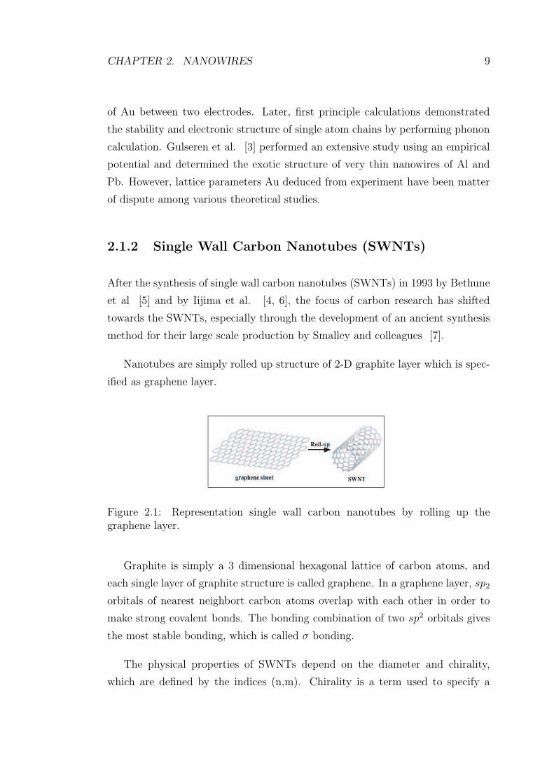
Nanotubes are simply rolled up structure of 2-D graphite layer which is spec-
ified as graphene layer.
Figure 2.1: Representation single wall carbon nanotubes by rolling up thegraphene layer.
Graphite is simply a 3 dimensional hexagonal lattice of carbon atoms, and
each single layer of graphite structure is called graphene. In a graphene layer, sp2
orbitals of nearest neighbort carbon atoms overlap with each other in order to
make strong covalent bonds. The bonding combination of two sp2 orbitals gives
the most stable bonding, which is called σ bonding.
The physical properties of SWNTs depend on the diameter and chirality,
which are defined by the indices (n,m). Chirality is a term used to specify a
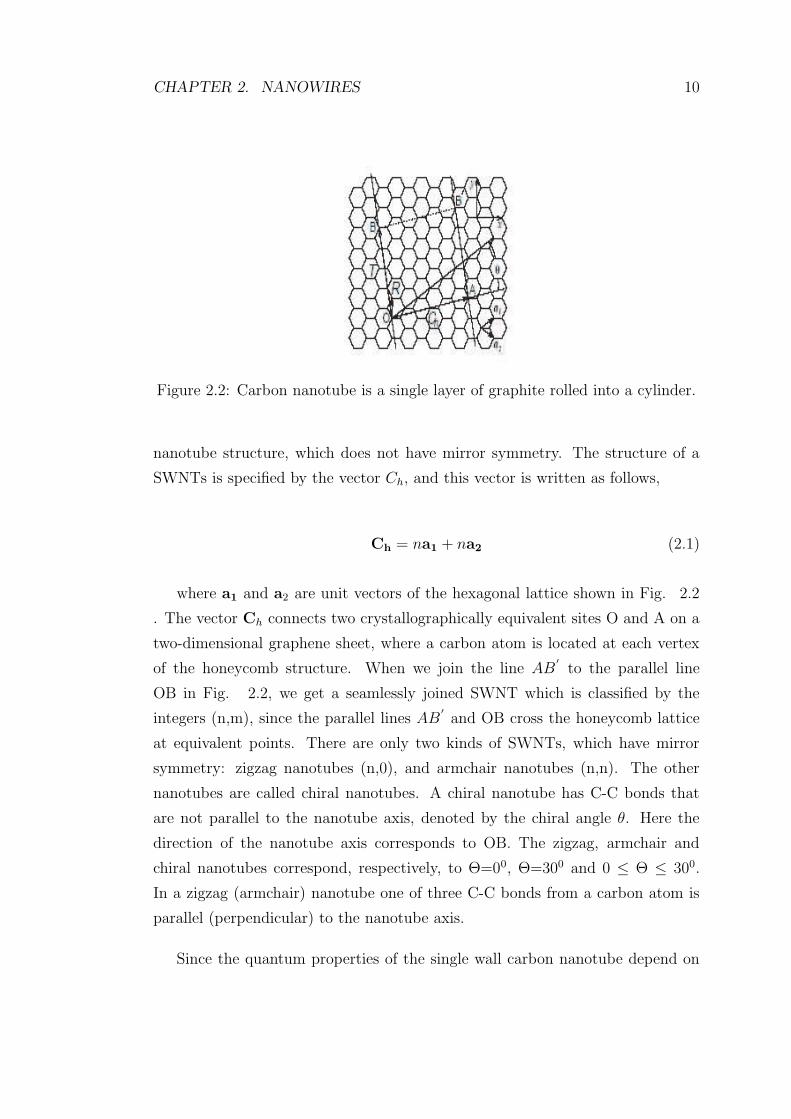
CHAPTER 2. NANOWIRES 10
Figure 2.2: Carbon nanotube is a single layer of graphite rolled into a cylinder.
nanotube structure, which does not have mirror symmetry. The structure of a
SWNTs is specified by the vector Ch, and this vector is written as follows,
Ch = na1 + na2 (2.1)
where a1 and a2 are unit vectors of the hexagonal lattice shown in Fig. 2.2
. The vector Ch connects two crystallographically equivalent sites O and A on a
two-dimensional graphene sheet, where a carbon atom is located at each vertex
of the honeycomb structure. When we join the line AB′
to the parallel line
OB in Fig. 2.2, we get a seamlessly joined SWNT which is classified by the
integers (n,m), since the parallel lines AB′
and OB cross the honeycomb lattice
at equivalent points. There are only two kinds of SWNTs, which have mirror
symmetry: zigzag nanotubes (n,0), and armchair nanotubes (n,n). The other
nanotubes are called chiral nanotubes. A chiral nanotube has C-C bonds that
are not parallel to the nanotube axis, denoted by the chiral angle θ. Here the
direction of the nanotube axis corresponds to OB. The zigzag, armchair and
chiral nanotubes correspond, respectively, to Θ=00, Θ=300 and 0 ≤ Θ ≤ 300.
In a zigzag (armchair) nanotube one of three C-C bonds from a carbon atom is
parallel (perpendicular) to the nanotube axis.
Since the quantum properties of the single wall carbon nanotube depend on

CHAPTER 2. NANOWIRES 11
the diameter and chirality, it will be suitable to indicate the diameter of a (n,m)
nanotube dt,
dt = Ch/π =√
3ac−c(m2 + mn + n2)1/2/π (2.2)
where ac−c is the nearest-neighbour C-C distance (1.42 Angstrom in graphite),
and Ch is the lenght of the chiral vector Ch. The chiral angle θ can be given by,
θ = tan−1[√
3m/(m + 2n)]] (2.3)
Figure 2.3: A (5,5) armchair nanotube (top), a (9,0) zigzag nanotube (middle)and a (10,5) chiral nanotube.
The electronic structure of SWNTs can be summarized as follows: In general,
(n,m) tubes with n-m=3q (n − m 6= 3q), where q is an integer are metallic
(semiconductor) [8]. Hence armchair nanotubes with (n,n) are metallic while
zigzag nanotubes with (n,0) are metallic or semiconductor depending on whether
n=3q or not. This behavior of nanotubes can be explained by zone-folding and
the curvature effects [8].
CHAPTER 2. NANOWIRES 12
2.1.3 Functionalized SWNTs
Physical properties of SWNTs can be modified by the adsorption of a foreign atom
or molecule on the surface of the tube. Adsorption can take plane externally or
internally. For example the band gap of a zigzag tube can be reduced by coverage
of O2. Exohydrogenation, i.e hydrogen atom coverage of a zigzag tube leads to
the widening of the band gap. Transition metal adsorption give rise to permanent
magnetic moment. The modification of physical properties through adsorption
of atoms or molecules is called functionalization of SWNT [9].
2.1.4 Coated Carbon Nanotubes
Coating of SWNTs (i.e, molecular or multilayer atom adsorption on SWNTs) is of
particular interest in the context of nanowires or conductors. It has been shown
experimentally that semiconducting SWNTs can be coated quite uniformly by Ti
atoms.First principle calculations by Dag et al [10]. have shown that (8,0) tube
can be uniformly covered by Ti atoms, and becomes a good conductor. Those
studies clearly showed that metal atom coating of SWNTs can be used to formate
interconnects with reproducible properties. Not all the atom can form uniform
coverage, they rather appear as small particles on the surface of the SWNT. For
example, good conductors such as Au, Ag and Cu cannot make uniform coating.
This difficulty can be overcome by the coating of Au and Ag on the buffer layer
of Ti or Ni, that can make uniform coverage of the surface of the tube.
SWNT coated by transition metal atoms are used not only for conductors,
but for nanomagnets. The first principle calculations reveals that net magnetic
moment can be created upon the coating of SWNT by atom such as Ti, Co, Cr
etc.
CHAPTER 2. NANOWIRES 13
2.2 Physical Properties of Nanowires
2.2.1 Electronic Structure
A finite nanowire between two metal electrodes displays discrete energy spec-
trum. The energy level spacing decreases as the number of atoms in the wire
increases. As the lenght of nanowire increases these energy levels can be de-
scribed by a band having dispersion along the axis of the wire. Under these
circumstances, the wave vector along the axis starts to be a good quantum num-
ber. If the wire consists of a few atoms, the energy states give rise to resonances.
2.2.2 Quantum Conductance
The discrete nature of electronic and phononic states of nanowire connecting two
electrodes reflects to the electrical and thermal conductance between two elec-
trodes connected by this wire. At the end it yields resorvable effects in measured
conductance.
The conductance of large samples obeys Ohm’s law, namely, G=σS/L, where
S is the cross section and L is the lenght. At microscopic scale, which are mea-
sured in nanometer, the behavior of conductance, namely its variation with the
L or S differs from that in macroscopic scale. Firstly there is an interface resis-
tance independent of the lenght L of the sample. Secondly the conductance does
not decrease uniformly with the width W. Instead it depends on the number of
transverse modes in the conductor and goes down in discrete steps (of quantum
conductance 2e2/h). The Landauer formula incorporates both of these features
[37].
G =2e2
h
∑niTi (2.4)

CHAPTER 2. NANOWIRES 14
Here ni is the degeneracy of the propagating modes, and the factor T transmis-
sion coefficient, i.e. represents the average probability that an electron injected
at one end of the conductor will transmit to the other end through the channel
i. If the transmission probability is unity, then we recover the correct expression
for the resistance of a ballistic conductor.
After introducing Landauer formula, now we can discuss the conductance of
nanotubes and nanowires. The conductance of the (n,n) armchair SWNTs can
be estimated from the number of bands crossing EF . There are two px derived
bands at the Fermi level, one even and one odd parity under the n axial mirror
symmetries of the tube. Therefore one expects that a single armchair nanotube
has a conductance of (Te+To)G0 , where Te and To are the transmission coefficients
associated with parity. If the transmission coefficients are unity, we then get a
conductance of 2G0 where G0 = 2e2/h at the Fermi level. If we generalize this
for MWNTs which is composed of m individual tubes, each having two channels
at the Fermi level, the maximum ballistic conductance is thus 2mG0 However,
experiments showed G = G0 rather than G = 2G0
Figure 2.4: Conductance G at room temperature measured as a function of depthof immersion of the nanotube bundle into the liquid gallium. As the nanotubebundle is dipped into the liquid metal, the conductance increases in steps ofG0=2e2/h. The steps corresponds to different nanotubes coming successivelyinto the contact with the liquid. [11]
But this puzzling situation has been clarified by Ihm and Louie [12] The
CHAPTER 2. NANOWIRES 15
incident π* band electrons have a very high angular momentum with respect to
the tube axis, and these electrons go through the tube without being scattered by
the free electrons in surrounding metal and contribute a quantum unit (2e2/h)
to the conductance. On the other hand, the incident π band electrons, with
the pz atomic orbitals in phase along the tube circumference, experience strong
resonant back-scattering because the low-angular-momentum states at the Fermi
level have a dominantly metallic character in the nanotube jellium metal coexis-
tence region. So these results obtained by Ihm and Louie provide an explanation
for the experimentally observed conductance of one quantum unit instead of two
for nanotubes with one end dipped into liquid metal such as gallium. Fig. 2.4
Having discussed the quantum conductance of nanotubes, further discussion
about the quantum conductance of nanowires is in order. On the basis of ab
initio calculations it has been shown that the conductance depends on the va-
lence states as well as the site where the single atom is bound to the electrode
[13]. The coupling to electrodes and hence the transmission coefficients are ex-
pected to depend on the binding structure. Scheer et al [14] found a direct link
between valence orbitals and the number of conduction channels in the conduc-
tance through a single atom. Lang [15] calculated the conductance through a
single Na atom, as well as a monatomic chain comprising two, three and four Na
atoms between two jellium electrodes by using the Green’s function formalism.
He found an anomalous dependence of the conductance on the lenght of the wire.
The conductance through a single atom was low (about G0/3), but increased by
a factor of two in going from a single atom to the two-atom wire. This behavior
was explained as the incomplete valence resonance of a single Na atom interacting
with the continuum of states of the jellium electrodes. Each additional Na atom
modifies the electronic structure and shifts the energy levels. The closer a state
is to the Fermi level, the higher is its contribution to the electrical conductance.
According to the Kalmeyer-Laughlin theory [16], a resonance with the maximum
DOS at the Fermi level makes the highest contribution to the transmission; the
conductance decreases as the maximum shifts away from the Fermi level.
This explanation is valid for a single atom between two macroscopic electrodes
forming a neck with length l < λF . The situation is, however, different for long

CHAPTER 2. NANOWIRES 16
monatomic chains. Since the electronic energy structure of a short monatomic
chain varies with the number of atoms, the results are expected to change if one
goes beyond the jellium approximation and considers the details of the coupling of
chain atoms to the electrode atoms. It is also expected that the conductance will
depend on where the monatomic chain ends and where the jellium edge begins.
In fact, Yanson et al [17] argued that the conductance of the Na wire calculated
by Lang [18] is lower than the experimental value possibly due to the interface
taken with the jellium.
2.2.3 Thermal Conductance
In nanowires thermal transport occurs by phonons and electrons. In dielectric
wires the energy is transported only by phonons, but in metalic wires this trans-
portation occurs mainly by electrons, since phononic contribution is small. There-
fore, in discussing the thermal transportation through wires, it will be suitable
to distinguish the thermal conductance through electrons and phonons.
When the width of the constriction of lenght l and width w is in the range
of Fermi wavelength, the transverse motion of electrons confined to w becomes
quantized. The finite level spacing of the quantized electronic states reverberates
into the ballistic electron transport, and gives rise to resolvable quantum features
in the variation of electrical and thermal conductance.
The phononic thermal conductance through a perfect and infinite chain, Kp,
is calculated by Buldum, Ciraci and Fong [19] by using a model Hamiltonian
approach, has been expressed as
Kp =∑
(π2k2b/3h)T (2.5)
Accordingly the ballistic thermal conductance of each branch i of the uniform
and harmonic atomic chain is limited by the value K0 = π2k2bT/3h. It is indepen-
dent of any material parameter, and is linearly dependent on T = (TL + TR)/2.
CHAPTER 2. NANOWIRES 17
The total thermal conductance becomes Kp = NK0, where N is the total num-
ber of phonon branches. For an ideal 1D atomic chain, N=3, if the transverse
vibrations are allowed. Furthermore, Ozpineci and Ciraci [20], showed that
the phononic thermal conductance through dielectric atomic chain having 1-10
atoms exhibits features similar to that found in the ballistic electrical conductance
through similar atomic chains.

Chapter 3
Theoretical Background
3.1 Born-Oppenheimer Approximation
Since the electrons have small mass compared with mass of the nuclei, electrons
move much faster than nuclei. So this means that electrons have the ability
to follow the motion of the nuclei instantaneously, so they remain in the same
stationary state of the electronic Hamiltonian all the time [21].This stationary
state will vary in time because of the coulombic coupling of these two sets of
freedom. So this means that as the nuclei follow their dynamics, the free electrons
instantaneously adjust their wavefunction according to the nuclear wavefunction.
Within these conditions, full wavefunction can be expressed as follows;
Ψ(R,r,t) = Θ(R, t)Φ(R, r) (3.1)
Here nuclear wave function Θ(R, t) obeys the time-dependent Schrodinger
equation and electronic wave function Φ(R, r) is the m-th stationary state of
the electronic Hamiltonian where m is any electronic eigenstate, but most of the
applications in the literature are focused on the ground state, i.e m=0.
18

CHAPTER 3. THEORETICAL BACKGROUND 19
Since the nuclear wavefunction satisfies the time-dependent Schrodinger equa-
tion, we can easily construct the time-dependent Schrodinger equation. But solv-
ing this equation is a formidable task for mainly two reasons; first of all it is a
many-body equation in N (N:number of atoms) nuclear coordinates, where the
interaction potential being given in a implicit form. Secondly the determination
of the potential energy surface for every possible nuclear configuration R involves
MN times the electronic equation, where M is defined as typical number of grid
points. However in many cases of our interest this nuclear solution is not neces-
sary since the thermal wavelength for a particle of mass M is λT = ( e2
MkbT), so the
regions of space separated by more than λL do not exhibit quantum coherence
and potential energy surfaces in typical bonding environments are stiff enough to
localize the nuclear wavefunctions to large extent.
Assuming these approximations, now we are left with the problem of solving
the many-body electronic Schrodinger equation for fixed nuclear positions.
3.2 The Electronic Problem
Although we are left with only solving the electronic part, solving Schrodinger
equation for a system of N interacting particle electrons in an external field is
still very difficult problem in many-body theory. The numerical solution is known
only in the case of uniform electron gas (for atoms with small number of electrons
and for a few molecules). For getting the analytical solution we have to resort to
approximations.
To cope with many electron Hamiltonian in 1928 Hartree proposed that many-
electron wave function (electronic wavefunction) can be written as product one-
electron wave functions each of which satisfies one-particle Schrodinger equation
in an effective potential. [22]
Φ(R, r) = Πiϕ(ri) (3.2)
CHAPTER 3. THEORETICAL BACKGROUND 20
(− h2
2m∇2 + V
(i)eff (R, r))ϕi(r) = εiϕi(r) (3.3)
with effective potential
V(i)eff (R, r) = V (R, r) +
∫ ∑Nj 6=i ρj(r’)
|r − r’| dr’ (3.4)
where
ρj(r) = |φj(r)|2 (3.5)
is the electronic density associated with particle j. The second term in Eq. 3.4 is
the mean field potential and the third term is the interactions of one electron with
the other electrons in a mean field. But it should be noted that total energy of
the many-body system is not just the sum of the eigenvalues of Eq. 3.3 because
the formulation in terms of an effective potential makes the electron-electron
interaction to be counted twice. So that the correct expression for the energy is
written as
EH =N∑
i
εn − 1
2
∫ ∫ ρ(r)ρ(r’)
|r − r’| drdr’ (3.6)
where second term is correction due to effective potential as discussed above.
Wavefunctions Φi(r) and charge density ρ(r), as well as εi energies are determined
by using self-consistent field (SCF) method.
Hartree approximation can be improved by considering the fermionic nature
of electrons. Due to Pauli exclusion principle, two fermions (electrons in our case)
cannot occupy the same state with all of their quantum numbers are the same. In
this case electronic wavefunction in 3.2 becomes an antisymmetrized many-body
electron wavefunction in the form of a Slater determinant as follows;
Φ(R, r) =1√N !
φ1(r1) . . . φ1(rN)...
. . ....
φN(r1) . . . φN(rN)
(3.7)
This approximation is called Hartree-Fock (HF) and it explains particle ex-
change in an exact manner [23, 24]. It also provides a moderate description of
CHAPTER 3. THEORETICAL BACKGROUND 21
inter-atomic bonding but many-body correlations are completely absent. Re-
cently, the HF approximation is routinely used as a starting point for more ad-
vanced calculations. It should be also noted that although HF equations look
same as Hartree equations, there is an additional coupling term in the differential
equations.
Parallel to the development in electronic theory, Thomas and Fermi proposed,
at about same time as Hartree, that the full electron density was the fundamental
variable of the many-body problem, and derived a differential equation for the
density without referring to one-electron orbitals. Although, this theory which
known as Thomas-Fermi Theory [25, 26], did not include exchange and corre-
lation effects and was able to sustain bound states, it set up the basis of later
development of Density Functional Theory (DFT).
3.3 Density Functional Theory
The initial work on DFT was reported in two publications: first by Hohenberg-
Kohn in 1964 [27], and the next by Kohn-Sham in 1965 [28]. This was almost
40 years after Schrodinger (1926) had published his pioneering paper marking the
beginning of wave mechanics. Now Density Functional Theory is very powerful
method for solving N interacting electron system.
The total ground state energy of an inhomogeneous system composed by N
interacting electrons includes three terms, namely kinetic energy T , interaction
with external fields V and electron-electron interaction Uee;
E = 〈T 〉 + 〈V 〉 + 〈Uee〉 (3.8)
Before concentrating on the electron-electron interaction term, we can indicate
the kinetic energy and interaction with external fields terms as follows;
CHAPTER 3. THEORETICAL BACKGROUND 22
V =P∑
I=1
〈Φ|N∑
i=1
υ(ri − RI)|Φ〉 =P∑
I=1
∫ρ(r)υ(r − RI)dr (3.9)
T = 〈Φ|−h2
2m
N∑
i=1
∇2i |Φ〉 = − h2
2m
∫[∇2
rρ1(r, r′)]r′=rdr (3.10)
Returning back to electron-electron interaction term, this can be written by
considering the coulomb interaction between them,
Uee = 〈Φ|Uee|Φ〉 = 〈Φ|12
N∑
i=1
N∑
j 6=i
1
| (ri − rj) ||Φ〉 =
∫ ρ2(r, r′)
| (r − r′) |drdr′ (3.11)
By redefining ρ2(r, r′) by using the two-body direct correlation function g(r, r′)
and the one-body density matrix ρ(r, r′) as in Eq. 3.12, Eq. 3.11 simplify to
Eq. 3.13
ρ2(r, r′) =
1
2ρ(r, r)ρ(r, r′)g(r, r′) (3.12)
Uee =1
2
∫ ρ(r)ρ(r′)
| (r − r′) |drdr′ +1
2
∫ ρ(r)ρ(r′)
| (r − r′) | [g(r, r′) − 1]drdr′ (3.13)
It is obvious that the first term is the classical electrostatic interaction energy
corresponding to a charge distribution ρ(r) and the second term includes the clas-
sical and quantum correlation effects. By introducing exchange depletion written
in Eq. 3.14 instead g(r, r′), we achieve another expression for total energy of
many-body electronic system Eq. 3.15.
gx(r, r′) = 1 −
∑σ | ρHF
σ (r, r′) |2ρHF (r)ρHF (r′)
(3.14)
E = T + V +1
2
∫ ρ(r)ρ(r′)
| (r − r′) |drdr′ + Exc (3.15)
CHAPTER 3. THEORETICAL BACKGROUND 23
In this equation the last term corresponds to exchange and correlation energy,
and this can be expressed as follows,
Exc =1
2
∫ ρ(r)ρ(r′)
| (r − r′) | [g(r, r′) − 1]drdr′ (3.16)
3.3.1 Hohenberg-Kohn Formulation
The Hohenberg-Kohn [27] formulation of DFT can be explained by two theorems:
Theorem 1: The external potential is univocally determined by the electronic
density, except for a trivial additive constant.
Since ρ(r) determines V(r), then this also determines the ground state wave-
function and gives the full Hamiltonian for the electronic system. So that ρ(r)
determines implicitly all properties derivable from H through the solution of the
time-dependent Schrodinger equation.
Theorem 2: The minimal principle can be formulated in terms of trial charge
densities, instead of trial wavefunctions.
The ground state energy E could be obtained by solving the Schrodinger
equation directly or from the Rayleigh-Ritz minimal principle:
E = min〈Ψ|H|Ψ〉〈Ψ|Ψ〉
(3.17)
Using ρ(r) instead of Ψ(r) was first presented in Hohenberg and Kohn. For a
non-degenerate ground state, the minimum is attained when ρ(r) is the ground
state density. And energy is given by the equation:
EV [ρ] = F [ρ] +∫
ρ(r)V (r)dr (3.18)
with
F [ρ] = 〈Ψ[ρ]|T + U |Ψ[ρ]〉 (3.19)
and F [ρ] requires no explicit knowledge of V(r).
CHAPTER 3. THEORETICAL BACKGROUND 24
These two theorems form the basis of the DFT. The main remaining error
is due to inadequate representation of kinetic energy and it will be cured by
representing Kohn-Sham equations.
3.3.2 Kohn-Sham Equations
Thomas and Fermi gave a prescription for constructing the total energy in terms
only of electronic density by using the expression for kinetic, exchange and corre-
lation energies of the homogeneous electron gas to construct the same quan-
tities for the inhomogeneous system [28]. This was the first time that the
Local Density Approximation (LDA) was used. But this model is a severe short-
coming since this does not hold bound states and also the electronic structure is
absent!!!
W.Kohn and L.Sham then proposed that the kinetic energy of the interact-
ing electrons can be replaced with that of an equivalent non-interacting system
which can be calculated easily. With this idea, the density matrix ρ(r, r′) of an
interacting system can be written as sum of the spin up and spin down density
matrices,
ρs(r, r′) =
∞∑
i=1
ni,sΦi,s(r)Φ∗i,s(r
′) (3.20)
Where ni,s ar the occupation numbers of single particle orbitals, namely
Φi,s(r). Now the kinetic energy term can be written as Eq. 3.21
T =2∑
s=1
∞∑
i=1
ni,s〈Φi,s| −∇2
2|Φi,s〉 (3.21)
This expression can be developed by considering that the Hamiltonian has no
electron-electron interactions and thus eigenstates can now be expressed in the
form of Slater determinant. By using this argument the density is written as
CHAPTER 3. THEORETICAL BACKGROUND 25
ρ(r) =2∑
s=1
Ns∑
i=1
|ϕi,s(r)|2 (3.22)
and the kinetic term becomes
T [ρ] =2∑
s=1
Ns∑
i=1
〈ϕi,s| −∇2
2|ϕi,s〉 (3.23)
Now, we can write the total energy of the system which is indicated in Eq.
3.15 in terms only of electronic density as follows,
EKohn−Sham[ρ] = T [ρ] +∫
ρ(r)v(r)dr +1
2
∫ ∫ ρ(r)ρ(r′)
|r − r′| drdr′ + EXC [ρ] (3.24)
This equation is called the Kohn-Sham Equations After writing main equa-
tion, now the solution of the Kohn-Sham equations can be achieved by applying
the same iterative procedure, in the same way of Hartree and Hartree-Fock equa-
tions. As a remark after all, in this approximation we have expressed the density
functional in terms of KS orbitals which minimize the kinetic energy under the
fixed density constraint. In principle these orbitals are a mathematical object
constructed in order to render the problem more tractable, and do not have a
sense by themselves.
3.4 Exchange and Correlation
If we know the exact expression for the kinetic energy including correlation effects,
then we can use the original definition of the exchange-correlation energy E0XC [ρ]
which does not contain kinetic contributions.
E0XC [ρ] =
1
2
∫ ∫ ρ(r)ρ(r′)
| (r − r′) | [g(r, r′) − 1]drdr′ (3.25)
CHAPTER 3. THEORETICAL BACKGROUND 26
In this equation E0XC [ρ] is the exchange-correlation energy without kinetic
contributions. For writing the exchange-correlation energy EXC [ρ] as a function
of ρ, we redefine Eq. 3.25 by considering the non-interacting expression for the
kinetic energy TR[ρ] in the following way,
EXC [ρ] = E0XC [ρ] + T [ρ] − TR[ρ] (3.26)
In this equation second term is interacting kinetic energy with correlation ef-
fects, while the last term corresponds to non-interacting kinetic energy. These
two term can be considered as a modification to two-body correlation function
g(r, r′) in Eq. 3.25. Updated two-body correlation function is now called as
average of pair correlation function, and the exchange-correlation energy with ki-
netic contribution can be written as,
EXC [ρ] =1
2
∫ ∫ ρ(r)ρ(r′)
| (r − r′) | [g(r, r′) − 1]drdr′ (3.27)
where g(r, r′) can be expressed as follows,
g(r, r′) = 1 −∑
σ | (ρσ(r, r′) |2)ρ(r)ρ(r′)
+ ˜gxc(r, r′) (3.28)
For further simplification for EXC [ρ], the exchange-correlation hole ˜gxc(r, r′)
is defined
˜gxc(r, r′) = ρ(r′)[g(r, r′) − 1] (3.29)
so EXC [ρ] becomes,
EXC [ρ] =1
2
∫ ∫ ρ(r) ˜gxc(r, r′)
| (r − r′) | drdr′ (3.30)
CHAPTER 3. THEORETICAL BACKGROUND 27
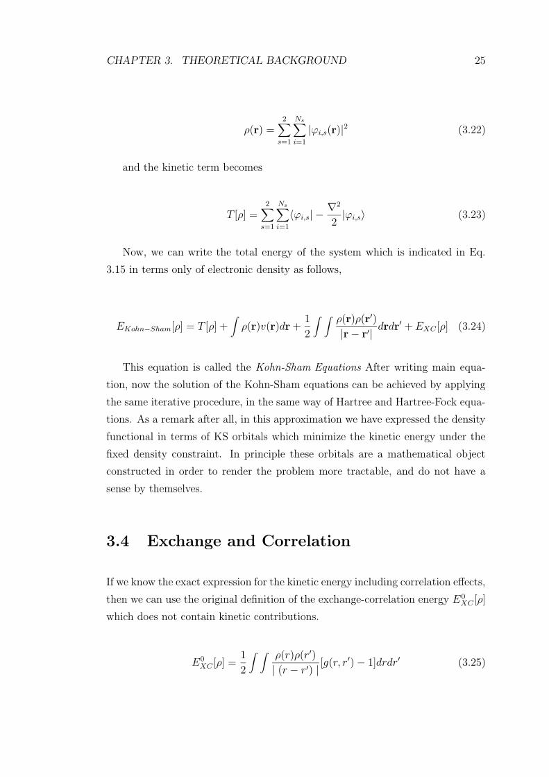
Having discussed fundamental equations of DFT, we introduce next the
Local Density Approximation (LDA) and Generalized Gradient Approximation
(GGA)
3.4.1 Local Density Approximation (LDA)
The local density approximation has been the most widely used approximation
to handle exchange correlation energy. It has been proposed in the seminal paper
by Kohn and Sham, but the philosophy was already present in Thomas-Fermi
theory. In Local Density Approximation, the exchange-correlation energy of an
electronic system is constructed by assuming that the exchange-correlation energy
per electron at a point ρ in the electron gas, is equal to the exchange-correlation
energy per electron in a homogeneous electron gas that has the same electron
density at the point ρ. In fact LDA based on two main approximations, (1) The
pair function is approximated by that of the homogeneous electron gas density
ρ(r) corrected by the density ratio ρ(r)/ρ(r′) to compansate the fact that the
LDA exchange-correlation hole is now centered at r instead of r′ (2) The LDA
exchange-correlation hole interacts with the electronic density at r, and is centered
at r. But as we know that the real exchange-correlation hole is actually centered
at r′ instead r.
Figure 3.1: Schematic representation of Local Density Approximation

CHAPTER 3. THEORETICAL BACKGROUND 28
3.4.2 Generalized Gradient Approximation (GGA)
Although the LDA was the universal choice for ab-initio calculations on amor-
phous systems, there were well known problems with the approximation: (1)
First of all in the local density approximation the optical gap is always poorly es-
timated (normally underestimated). Of course, this does not affect ground state
properties like charge density, total energy and forces, but it serious problem for
calculations of conduction states, as for example in the case of transport or opti-
cal properties.(2) In strongly (electronically) inhomogeneous systems such as SiO,
the basic assumption of weak spatial variation of the charge density is not well
satisfied, hence the LDA has difficulty. (3) The LDA assumes that the system
is paramagnetic; the local spin density approximation [34] (LSDA) (in which
a separate “spin up” and “spin down” density functional is used) is useful for
systems with unpaired spins, as for example a half filled state at the Fermi level.
Several workers, but especially Perdew [35], have worked on next
step to the LDA: inclusion of effects proportional to the gradient of
the charge density. Recent improvements along these ways are called
Generalized Gradient Approximations (GGA), it seems that these have led to
significant improvements in SiO [36], and intermolecular binding in water is
better described with GGA than in the LDA. In some ways the GGA has been
disappointing; on very precise measurements on molecules the results have been
mixed. But overall, the GGA seems to be an improvement over the conventional
LDA.
In GGA exchange-correlation energy can be written as follows,
EXC [ρ] =∫
ρ(r)εXC [ρ(r)]dr +∫
FXC [ρ(r,∇ρ(r))]dr (3.31)
where the function FXC is asked to satisfy the formal conditions.
GGA approximation improves binding energies, atomic energies, bond lengths
and bond angles when compared the ones obtained by LDA. In our calculations,
we used the GGA approximation [45].

CHAPTER 3. THEORETICAL BACKGROUND 29
Figure 3.2: Summary of the electron-electron interactions where the coulombicinteractions excluded. (a) the Hartree approximation, (b) the Hartree-Fock ap-proximation, (c) the local density approximation and (d) the local spin densityapproximation which allows for different interactions for like-unlike spins.
As a summary of all approximations Fig. 3.2 will be useful for the reader.
3.5 Other Details of Calculations
By using the represented formalisms observables of many-body systems can be
transformed into single particle equivalents. However, there still remains two
difficulties: A wave function must be calculated for each of the electrons in the
system and the basis set required to expand each wave function is infinite since
they extend over the entire solid.
k-point Sampling : Electronic states are only allowed at a set of k-points
determined by boundary conditions. The density of allowed k-points are propor-
tional to the volume of the cell. The occupied states at each k-point contribute to
the electronic potential in the bulk solid, so that in principle, an finite number of
calculations are needed to compute this potential. However, the electronic wave
functions at k-points that are very close to each other, will be almost identical.
CHAPTER 3. THEORETICAL BACKGROUND 30
Hence, a single k-point will be sufficient to represent the wave functions over a
particular region of k-space. There are several methods which calculate the elec-
tronic states at special k-points in the Brillouin zone [47]. Using these methods
one can obtain an accurate approximation for the electronic potential and total
energy at a small number of k-points. The magnitude of any error can be reduced
by using a denser set k-points.
Plane-wave Basis Sets : According to Bloch‘s theorem, the electronic wave
functions at each k-point can be extended in terms of a discrete plane-wave basis
set. Infinite number of plane-waves are needed to perform such expansion. How-
ever, the coefficients for the plane waves with small kinetic energy (h2/2m)|k+G|2
are more important than those with large kinetic energy. Thus some particular
cutoff energy can be determined to include finite number of k-points. The trun-
cation of the plane-wave basis set at a finite cutoff energy will lead to an error in
computed energy. However, by increasing the cutoff energy the magnitude of the
error can be reduced.
Plane-wave Representation of Kohn-Sham Equations : When plane
waves are used as a basis set, the Kohn-Sham(KS) [28] equations assume a par-
ticularly simple form. In this form, the kinetic energy is diagonal and potentials
are described in terms of their Fourier transforms. Solution proceeds by diago-
nalization of the Hamiltonian matrix. The size of the matrix is determined by
the choice of cutoff energy, and will be very large for systems that contain both
valence and core electrons. This is a severe problem, but it can be overcome by
considering pseudopotential approximation.
Nonperiodic Systems : Bloch theorem cannot be applied to a non-periodic
systems, such as a system with a single defect. A continuous plane-wave basis set
would be required to solve such systems. Calculations using plane-wave basis sets
can only be performed on these systems if a periodic supercell is used. Periodic
boundary conditions are applied to supercell so that the supercell is reproduced
through out the space. As seen schematically in Fig. 3.3 even a molecule can be
studied by using a supercell which prevents interactions between molecules.
Pseudopotential Approximation : Numerically and mathematically, a
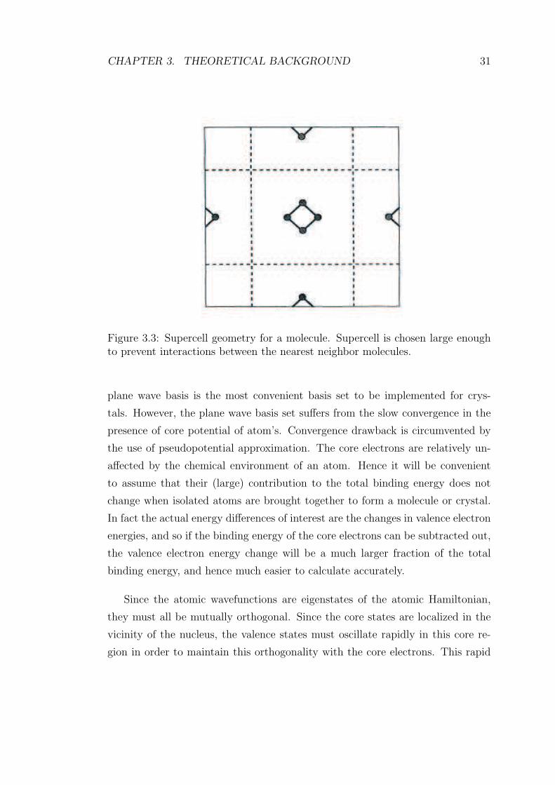
CHAPTER 3. THEORETICAL BACKGROUND 31
Figure 3.3: Supercell geometry for a molecule. Supercell is chosen large enoughto prevent interactions between the nearest neighbor molecules.
plane wave basis is the most convenient basis set to be implemented for crys-
tals. However, the plane wave basis set suffers from the slow convergence in the
presence of core potential of atom’s. Convergence drawback is circumvented by
the use of pseudopotential approximation. The core electrons are relatively un-
affected by the chemical environment of an atom. Hence it will be convenient
to assume that their (large) contribution to the total binding energy does not
change when isolated atoms are brought together to form a molecule or crystal.
In fact the actual energy differences of interest are the changes in valence electron
energies, and so if the binding energy of the core electrons can be subtracted out,
the valence electron energy change will be a much larger fraction of the total
binding energy, and hence much easier to calculate accurately.
Since the atomic wavefunctions are eigenstates of the atomic Hamiltonian,
they must all be mutually orthogonal. Since the core states are localized in the
vicinity of the nucleus, the valence states must oscillate rapidly in this core re-
gion in order to maintain this orthogonality with the core electrons. This rapid
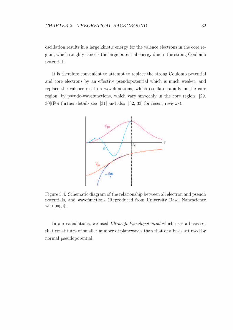
CHAPTER 3. THEORETICAL BACKGROUND 32
oscillation results in a large kinetic energy for the valence electrons in the core re-
gion, which roughly cancels the large potential energy due to the strong Coulomb
potential.
It is therefore convenient to attempt to replace the strong Coulomb potential
and core electrons by an effective pseudopotential which is much weaker, and
replace the valence electron wavefunctions, which oscillate rapidly in the core
region, by pseudo-wavefunctions, which vary smoothly in the core region [29,
30](For further details see [31] and also [32, 33] for recent reviews).
Figure 3.4: Schematic diagram of the relationship between all electron and pseudopotentials, and wavefunctions (Reproduced from University Basel Nanoscienceweb-page).
In our calculations, we used Ultrasoft Pseudopotential which uses a basis set
that constitutes of smaller number of planewaves than that of a basis set used by
normal pseudopotential.
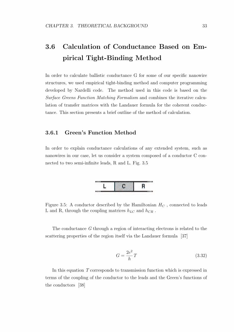
CHAPTER 3. THEORETICAL BACKGROUND 33
3.6 Calculation of Conductance Based on Em-
pirical Tight-Binding Method
In order to calculate ballistic conductance G for some of our specific nanowire
structures, we used empirical tight-binding method and computer programming
developed by Nardelli code. The method used in this code is based on the
Surface Greens Function Matching Formalism and combines the iterative calcu-
lation of transfer matrices with the Landauer formula for the coherent conduc-
tance. This section presents a brief outline of the method of calculation.
3.6.1 Green’s Function Method
In order to explain conductance calculations of any extended system, such as
nanowires in our case, let us consider a system composed of a conductor C con-
nected to two semi-infinite leads, R and L. Fig. 3.5
Figure 3.5: A conductor described by the Hamiltonian HC , connected to leadsL and R, through the coupling matrices hLC and hCR .
The conductance G through a region of interacting electrons is related to the
scattering properties of the region itself via the Landauer formula [37]
G =2e2
hT (3.32)
In this equation T corresponds to transmission function which is expressed in
terms of the coupling of the conductor to the leads and the Green’s functions of
the conductors [38]
CHAPTER 3. THEORETICAL BACKGROUND 34
T = Tr(ΓLgrCΓRga
C) (3.33)
where Γ[L,R] are functions that describe the coupling of the conductor to the
leads and g[r,a]C are the retarded and advanced Green’s functions. The Green’s
function of the conductor can be computed starting from the following equation
for the Green’s function of the whole system,
(ε − H)g = I (3.34)
where ε = E−iη with η arbitrarily small, and I is the identity matrix. In here,
Green’s function of the whole system (g) can be separated into submatrices that
corresponds to Green’s functions of individual subsystems. Further calculation
steps give us, G which is the conductance of conductor C shown in Fig. 3.5
As seen the core of the problem lies in the calculation of the Greens functions
of the semi-infinite leads (further details about method for solving this problem
can be found at [39]). It should be noted that the solution of Green’s functions,
requires Hamiltonian matrix, H. This Hamiltonian matrix of the system can be
determined by Empirical Tight-Binding approach. After constructing H, Green’s
functions, T transmission function and finally conductance G can be determined
by making use of last three equations.
3.6.2 Empirical Tight-Binding Method (ETB)
The empirical or parameterized tight-binding method (ETB) has been employed
extensively in the past for the study of semiconductors due to the simplicity of
the approach and its ability to describe properties in terms of chemical bonds.
This gives the model a more realistic nature as opposed to methods based on
weak periodic potentials. The ETB approach is suitable to deal with larger
systems compared to the first-principles methods based on plane waves, due to
the relatively lower computation time. The ETB method was originally described

CHAPTER 3. THEORETICAL BACKGROUND 35
by Slater and Koster [40] as an interpolation scheme. It has been developed
extensively since then and is now a well established technique to elucidate the
electronic structure of solids. Wavefunction of the system can be written as,
Ψ(r) =∑
R
eik·RΦ(r − R) (3.35)
where Φ(r − R) are atomic orbitals (s,px, py, pz). The Hamiltonian of the
system can be composed of the Hamiltonian, Hat, of single atom at the atomic
site and all corrections to the atomic potential at the interatomic region ∆[U(r)]
to produce the full periodic potential of the system.
H ∼= Hat + ∆[U(r)] (3.36)
By using this idea, now we can easily construct the Hamiltonian matrix of the
system. Normally, each element of Hamiltonian matrix (Hij) is calculated by the
following integral,
Hij =∫
Ψ∗
iHΨjdr3 (3.37)
However this integration is not so simple and requires three dimensional multi
center integrals. Therefore, instead of computing the integral, one can represent it
by some parameters, i.e tight-binding parameters [41, 42, 43]. Number of these
parameters depends on the approximation (i.e first nearest or second nearest
neighbor interaction or etc.). In the present thesis up to second nearest neighbor
interaction have been taken into account. Therefore 12 different tight-binding
parameters Es, Epx, Epy
, Epz, Vssσ1
, Vssσ2, Vspσ1
, Vspσ2, Vppσ1
, Vppσ2, Vppπ1
, Vppπ2must
be fitted to the known electronic energy band values (obtained from ab-initio
calculations or experimental measurements).

Chapter 4
Results and Discussion
4.1 Motivation
The structure of nanowires itself is important. The stability and periodicity of
the atomic structure in one dimension (1D) is of academical and technological
interest, because of our limited knowledge in one-dimensional crystallography.
Besides, earlier research have argued that at D ∼ λB, the conductance G (even the
diameter D or size) of nanowires are quantized. Group IV elements, Carbon and
Silicon, make semiconductor an insulator in diamond structure, because of their
even number of valence electrons appropriate for tetrahedrally directed covalent
bonds. Now it’s of interest to find their electronic properties when they form very
thin nanowires. Possible conductors predicted from these nanowires are expected
to be important in microelectronics, which aims at to fabricate device with with
dimensions less than 200A.
36

CHAPTER 4. RESULTS AND DISCUSSION 37
4.2 Method of calculations
Our study deals with physical properties of various carbon and silicon nanowire
structures from linear chain to hexagonal structure The physical properties com-
prise optimized atomic structure, electronic Energy bands, bonding and cohesive
energy, conductance and metallicity. The binding energy and resulting electronic
structure of any stable structure have been calculated by using a first-principles
pseudopotential plane wave method within the generalized gradient approxima-
tion (GGA) [45].
In our first-principle calculations, we used ultrasoft pseudopotential [46] and
plane waves up to an energy cutoff of 330 eV depending on the element. The Bril-
louin zone (BZ) of the supercell is sampled by (1,1,11) to (1,1,41) k-points within
the Monkhorst-Pack special k–point scheme depending on the element type and
the size of (BZ) [47]. Convergence tests have been performed with respect to
the energy cutoff and number of k-points. Calculations have been performed in
momentum space by using periodically repeating tetragonal supercell with lattice
constants, as = bs ∼ 10 whereby interaction of nearest neighbors in the x and
y directions are negligible. The lattice constant along the axis of the nanowire
structure coincides with the lattice constant of supercell cs. In our calculation,
we optimized the lattice constant c of the wire by optimizing the lattice constant
cs of the supercell. To enhance the variational freedom in the atomic geometry,
we examinedd certain structures in double supercell with cs = 2c.
4.3 Carbon and Silicon Nanowires
4.3.1 Linear Chain C1 and Si1
In order to find the electronic properties of carbon and silicon linear chain (C1
and Si1), we first optimized its structure. This structure is relaxed by selecting
the appropriate number of k-points and energy cutoff values determined from
convergence tests. Number of k-points used in Brillouin zone sampling and energy
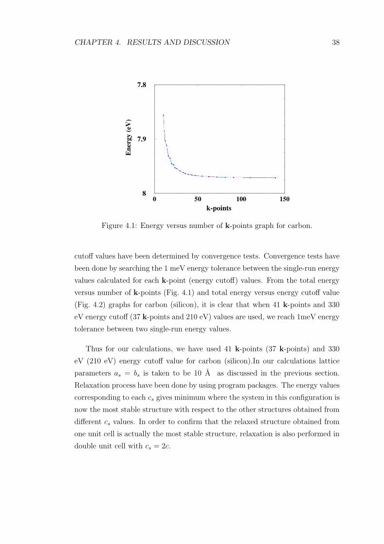
CHAPTER 4. RESULTS AND DISCUSSION 38
0 50 100 150k-points
8
7.9
7.8
Ene
rgy
(eV
)
Figure 4.1: Energy versus number of k-points graph for carbon.
cutoff values have been determined by convergence tests. Convergence tests have
been done by searching the 1 meV energy tolerance between the single-run energy
values calculated for each k-point (energy cutoff) values. From the total energy
versus number of k-points (Fig. 4.1) and total energy versus energy cutoff value
(Fig. 4.2) graphs for carbon (silicon), it is clear that when 41 k-points and 330
eV energy cutoff (37 k-points and 210 eV) values are used, we reach 1meV energy
tolerance between two single-run energy values.
Thus for our calculations, we have used 41 k-points (37 k-points) and 330
eV (210 eV) energy cutoff value for carbon (silicon).In our calculations lattice
parameters as = bs is taken to be 10 A as discussed in the previous section.
Relaxation process have been done by using program packages. The energy values
corresponding to each cs gives minimum where the system in this configuration is
now the most stable structure with respect to the other structures obtained from
different cs values. In order to confirm that the relaxed structure obtained from
one unit cell is actually the most stable structure, relaxation is also performed in
double unit cell with cs = 2c.

CHAPTER 4. RESULTS AND DISCUSSION 39
200 300 400 500Cutoff energy values (eV)
7.97
7.96
7.95
Ene
rgy
(eV
)
Figure 4.2: Energy versus energy cutoff value graph for carbon.
The optimized structures of C1 and Si1 obtained from first-principle pseu-
dopotential method are shown in Fig. 4.3
Figure 4.3: Relaxed structure of C1 and Si1 in double unit cell with latticeparameters as = bs = 10 A, cs = 2 · 1.269 A and binding energy Ebinding = 8.29eV/atom for relaxed C1 structure, and as=bs=10 A, c = 2·2.217A, Ebinding = 3.45eV/atom for Si1 relaxed structure. Supercell is defined by lateral black lines.
Although the atomic structures determined by using Congugate Gradient
(CG) method is generally stable, we performed further stability tests of the
structures. This way, we excluded the probability the CGA optimized structures
corresponds to metastable structure.
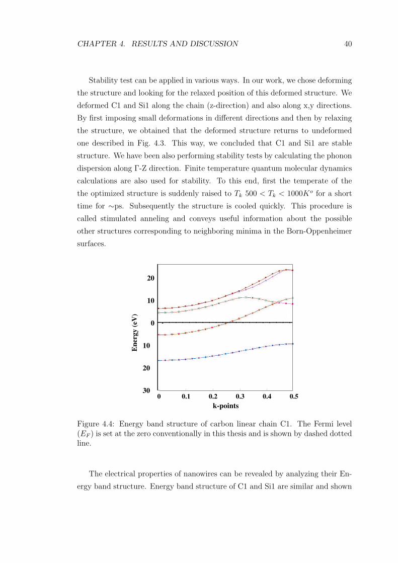
CHAPTER 4. RESULTS AND DISCUSSION 40
Stability test can be applied in various ways. In our work, we chose deforming
the structure and looking for the relaxed position of this deformed structure. We
deformed C1 and Si1 along the chain (z-direction) and also along x,y directions.
By first imposing small deformations in different directions and then by relaxing
the structure, we obtained that the deformed structure returns to undeformed
one described in Fig. 4.3. This way, we concluded that C1 and Si1 are stable
structure. We have been also performing stability tests by calculating the phonon
dispersion along Γ-Z direction. Finite temperature quantum molecular dynamics
calculations are also used for stability. To this end, first the temperate of the
the optimized structure is suddenly raised to Tk 500 < Tk < 1000Ko for a short
time for ∼ps. Subsequently the structure is cooled quickly. This procedure is
called stimulated anneling and conveys useful information about the possible
other structures corresponding to neighboring minima in the Born-Oppenheimer
surfaces.
0 0.1 0.2 0.3 0.4 0.5k-points
30
20
10
0
10
20
Ene
rgy
(eV
)
Figure 4.4: Energy band structure of carbon linear chain C1. The Fermi level(EF ) is set at the zero conventionally in this thesis and is shown by dashed dottedline.
The electrical properties of nanowires can be revealed by analyzing their En-
ergy band structure. Energy band structure of C1 and Si1 are similar and shown
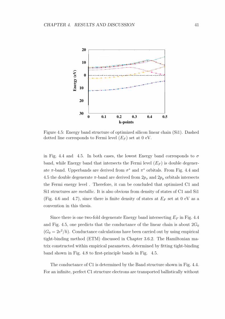
CHAPTER 4. RESULTS AND DISCUSSION 41
0 0.1 0.2 0.3 0.4 0.5k-points
30
20
10
0
10
20
Ene
rgy
(eV
)
Figure 4.5: Energy band structure of optimized silicon linear chain (Si1). Dasheddotted line corresponds to Fermi level (EF ) set at 0 eV.
in Fig. 4.4 and 4.5. In both cases, the lowest Energy band corresponds to σ
band, while Energy band that intersects the Fermi level (EF ) is double degener-
ate π-band. Upperbands are derived from σ∗ and π∗ orbitals. From Fig. 4.4 and
4.5 the double degenerate π-band are derived from 2px and 2py orbitals intersects
the Fermi energy level . Therefore, it can be concluded that optimized C1 and
Si1 structures are metallic. It is also obvious from density of states of C1 and Si1
(Fig. 4.6 and 4.7), since there is finite density of states at EF set at 0 eV as a
convention in this thesis.
Since there is one two-fold degenerate Energy band intersecting EF in Fig. 4.4
and Fig. 4.5, one predicts that the conductance of the linear chain is about 2G0
(G0 = 2e2/h). Conductance calculations have been carried out by using empirical
tight-binding method (ETM) discussed in Chapter 3.6.2. The Hamiltonian ma-
trix constructed within empirical parameters, determined by fitting tight-binding
band shown in Fig. 4.8 to first-principle bands in Fig. 4.5.
The conductance of C1 is determined by the Band structure shown in Fig. 4.4.
For an infinite, perfect C1 structure electrons are transported ballistically without
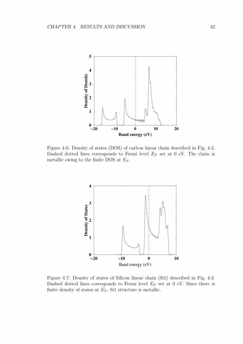
CHAPTER 4. RESULTS AND DISCUSSION 42
−20 −10 0 10 20Band energy (eV)
0
1
2
3
4
5
Den
sity
of D
ensi
ty
Figure 4.6: Density of states (DOS) of carbon linear chain described in Fig. 4.3.Dashed dotted lines corresponds to Fermi level EF set at 0 eV. The claim ismetallic owing to the finite DOS at EF .
−20 −10 0 10Band energy (eV)
0
1
2
3
4
Den
sity
of S
tate
s
Figure 4.7: Density of states of Silicon linear chain (Si1) described in Fig. 4.3.Dashed dotted lines corresponds to Fermi level EF set at 0 eV. Since there isfinite density of states at EF , Si1 structure is metallic.

CHAPTER 4. RESULTS AND DISCUSSION 43
0 0.1 0.2 0.3 0.4 0.5k-points
30
20
10
0
10
20
Ene
rgy
(eV
)
Figure 4.8: The band-structure of C1 calculated by emprical tight-bindingmethod (ETB) fitted to first-principle band structure shown in Fig. 4.4. + indi-cate the first-principle band energies. EF shown by dashed dotted line set at 0 eV.Tight-binding parameters are: Es = −17.096 eV,Ep1 = −3.545 eV,Ep2 = 3.282eV,Vssσ = −1.559 eV,Vspσ = 1.463 eV,Vppσ = −1.276 eV,Vppπ = −3.827eV,Vssσ = 0.256 eV,Vspσ = 0.956 eV,Vppσ = −1.228 eV,Vssσ = −0.841 eV, wherethe last four parameters obtained from second nearest interaction.
any scattering. Under these circumstances the mean free path, lm ∼ ∞. Under
a finite bias voltage Vb, the conductance of G of C1 are calculated by the tight-
binding Green’s function (TBGF) technique using program developed by Nardelli.
In this calculation of Green’s function the tight-binding band structure of C1 is
essential to this and the ab-initio band structure of C1 in Fig. 4.4 is fitted to a
tight-binding band shown in Fig. 4.8. In Fig. 4.8 the tight-binding band energies
are compared with first-principles band energies.
The conductance G versus Vb curve calculated for C1 by the TBGF method is
shown in Fig. 4.9. At Vb=0, the G(Vb)=2(2e2/h) since double degenerate π-band
crosses the Fermi level hence makes two current transporting states available for
conductance.
Similar calculation have been also carried out for Si1, and hence conductance
G versus Vb curve calculated by using the TBGF method is shown in Fig. 4.10.
Same interpretations for C1 structure are also valid for silicon linear chain Si1.
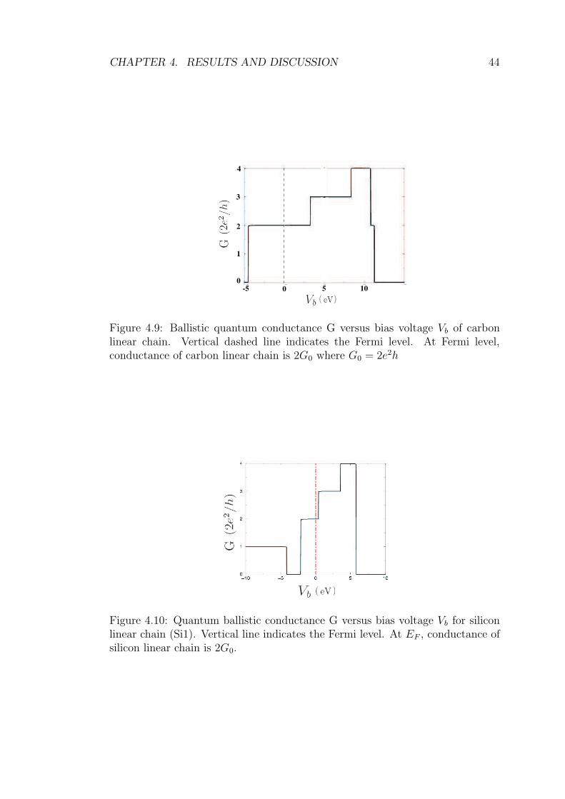
CHAPTER 4. RESULTS AND DISCUSSION 44
0-5 105
1
2
3
4
0
Figure 4.9: Ballistic quantum conductance G versus bias voltage Vb of carbonlinear chain. Vertical dashed line indicates the Fermi level. At Fermi level,conductance of carbon linear chain is 2G0 where G0 = 2e2h
Figure 4.10: Quantum ballistic conductance G versus bias voltage Vb for siliconlinear chain (Si1). Vertical line indicates the Fermi level. At EF , conductance ofsilicon linear chain is 2G0.
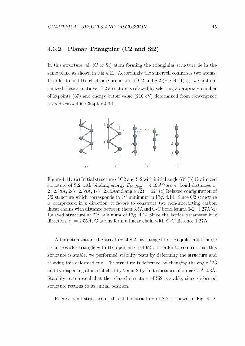
CHAPTER 4. RESULTS AND DISCUSSION 45
4.3.2 Planar Triangular (C2 and Si2)
In this structure, all (C or Si) atom forming the trianglular structure lie in the
same plane as shown in Fig 4.11. Accordingly the supercell comprises two atoms.
In order to find the electronic properties of C2 and Si2 (Fig. 4.11(a)), we first op-
timized these structures. Si2 structure is relaxed by selecting appropriate number
of k-points (37) and energy cutoff value (210 eV) determined from convergence
tests discussed in Chapter 4.3.1.
(a) (b) (c) (d)
1 1
1 2
3
2
2
Figure 4.11: (a) Initial structure of C2 and Si2 with initial angle 60o (b) Optimizedstructure of Si2 with binding energy Ebinding = 4.19eV/atom, bond distances 1-2=2.38A, 2-3=2.38A, 1-3=2.45Aand angle 123 = 62o (c) Relaxed configuration ofC2 structure which corresponds to 1st minimum in Fig. 4.14. Since C2 structureis compressed in z direction, it favors to construct two non-interacting carbonlinear chains with distance between them 3.5Aand C-C bond length 1-2=1.27A(d)Relaxed structure at 2nd minimum of Fig. 4.14 Since the lattice parameter in zdirection, cs = 2.55A, C atoms form a linear chain with C-C distance 1.27A
After optimization, the structure of Si2 has changed to the equilateral triangle
to an isosceles triangle with the opex angle of 62o. In order to confirm that this
structure is stable, we performed stability tests by deforming the structure and
relaxing this deformed one. The structure is deformed by changing the angle 123
and by displacing atoms labelled by 2 and 3 by finite distance of order 0.1A-0.3A.
Stability tests reveal that the relaxed structure of Si2 is stable, since deformed
structure returns to its initial position.
Energy band structure of this stable structure of Si2 is shown in Fig. 4.12.
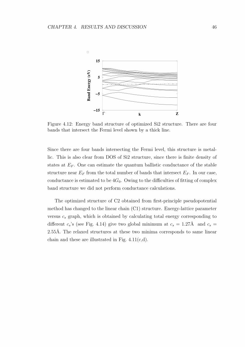
CHAPTER 4. RESULTS AND DISCUSSION 46
−15
−5
5
15
Ban
d E
nerg
y (e
V)
kΓ Z
Figure 4.12: Energy band structure of optimized Si2 structure. There are fourbands that intersect the Fermi level shown by a thick line.
Since there are four bands intersecting the Fermi level, this structure is metal-
lic. This is also clear from DOS of Si2 structure, since there is finite density of
states at EF . One can estimate the quantum ballistic conductance of the stable
structure near EF from the total number of bands that intersect EF . In our case,
conductance is estimated to be 4G0. Owing to the difficulties of fitting of complex
band structure we did not perform conductance calculations.
The optimized structure of C2 obtained from first-principle pseudopotential
method has changed to the linear chain (C1) structure. Energy-lattice parameter
versus cs graph, which is obtained by calculating total energy corresponding to
different cs’s (see Fig. 4.14) give two global minimum at cs = 1.27A and cs =
2.55A. The relaxed structures at these two minima corresponds to same linear
chain and these are illustrated in Fig. 4.11(c,d).

CHAPTER 4. RESULTS AND DISCUSSION 47
20 10 0 10 20Band energy (eV)
0
1
2
3
4
Den
sity
of s
tate
s
Figure 4.13: Calculated DOS of Si2 structure. There is finite density of states atthe Fermi level set at 0 eV, acoordingly this structure is metallic.
4.3.3 Zigzag Structure (C3 and Si3)
The zigzag structure can be described by isosceles triangular structure with large
apex angle (> 100o). It has two atoms in the supercell.
Silicon zigzag structure Si3 and carbon zigzag structure C3 shown in Fig. 4.15
are optimized. The optimized structure of Si3 obtained from the pseudopotential
method is illustrated in Fig. 4.15.
In the stability tests, Si3 is first deformed and subsequently is relaxed. The
displaced atoms have returned to its initial positions. Electronic properties of Si3
is studied by analyzing the band structure illustrated in Fig. 4.16. Since there is
no bands intersecting the Fermi level, this structure is semiconductor with band
gap Egap = 0.3eV .
Similar calculation steps also done for C3 structure, and we found that C3 is
not a stable structure, since this structure relaxes to C1.
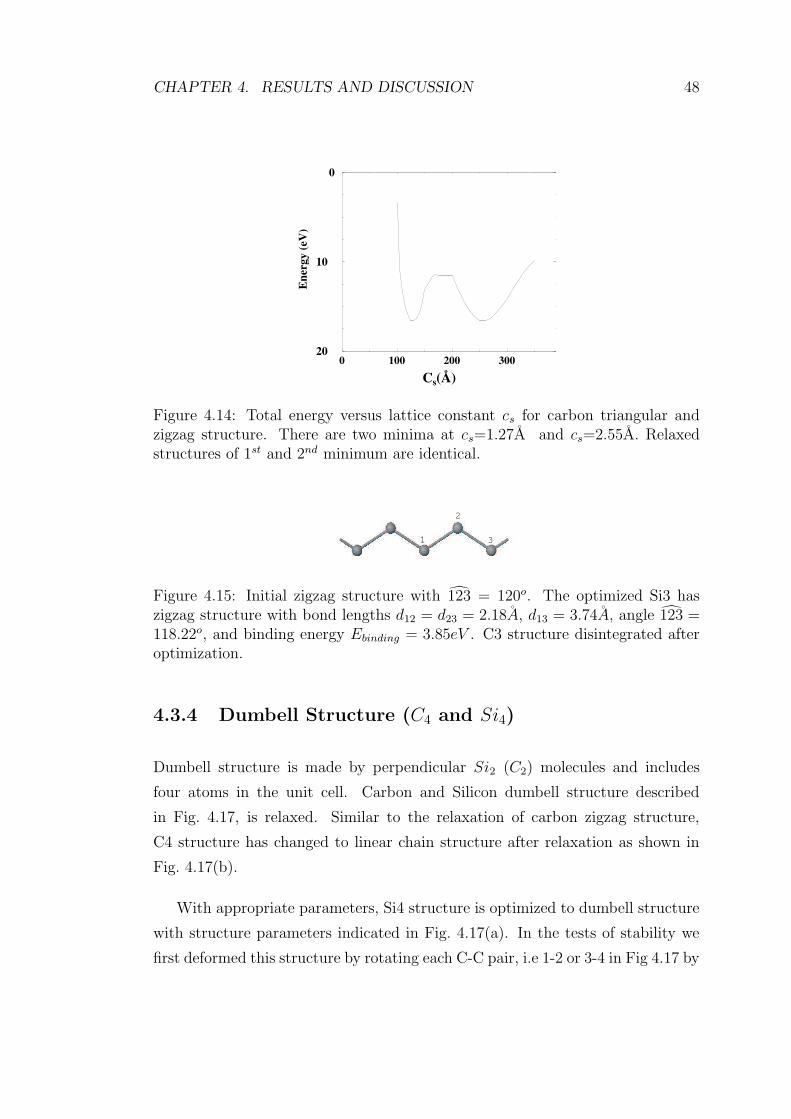
CHAPTER 4. RESULTS AND DISCUSSION 48
0 100 200 300
C (A)
20
10
0
Ene
rgy
(eV
)
so
Figure 4.14: Total energy versus lattice constant cs for carbon triangular andzigzag structure. There are two minima at cs=1.27A and cs=2.55A. Relaxedstructures of 1st and 2nd minimum are identical.
1
2
3
Figure 4.15: Initial zigzag structure with 123 = 120o. The optimized Si3 haszigzag structure with bond lengths d12 = d23 = 2.18A, d13 = 3.74A, angle 123 =118.22o, and binding energy Ebinding = 3.85eV . C3 structure disintegrated afteroptimization.
4.3.4 Dumbell Structure (C4 and Si4)
Dumbell structure is made by perpendicular Si2 (C2) molecules and includes
four atoms in the unit cell. Carbon and Silicon dumbell structure described
in Fig. 4.17, is relaxed. Similar to the relaxation of carbon zigzag structure,
C4 structure has changed to linear chain structure after relaxation as shown in
Fig. 4.17(b).
With appropriate parameters, Si4 structure is optimized to dumbell structure
with structure parameters indicated in Fig. 4.17(a). In the tests of stability we
first deformed this structure by rotating each C-C pair, i.e 1-2 or 3-4 in Fig 4.17 by
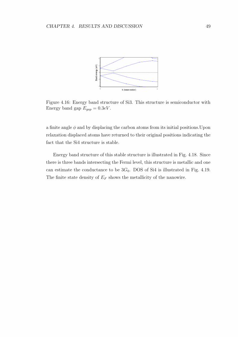
CHAPTER 4. RESULTS AND DISCUSSION 49
-2
-1
0
1
2
k (wave vector)
Ban
d en
ergy
(eV
)
Z G
Figure 4.16: Energy band structure of Si3. This structure is semiconductor withEnergy band gap Egap = 0.3eV .
a finite angle φ and by displacing the carbon atoms from its initial positions.Upon
relaxation displaced atoms have returned to their original positions indicating the
fact that the Si4 structure is stable.
Energy band structure of this stable structure is illustrated in Fig. 4.18. Since
there is three bands intersecting the Fermi level, this structure is metallic and one
can estimate the conductance to be 3G0. DOS of Si4 is illustrated in Fig. 4.19.
The finite state density of EF shows the metallicity of the nanowire.
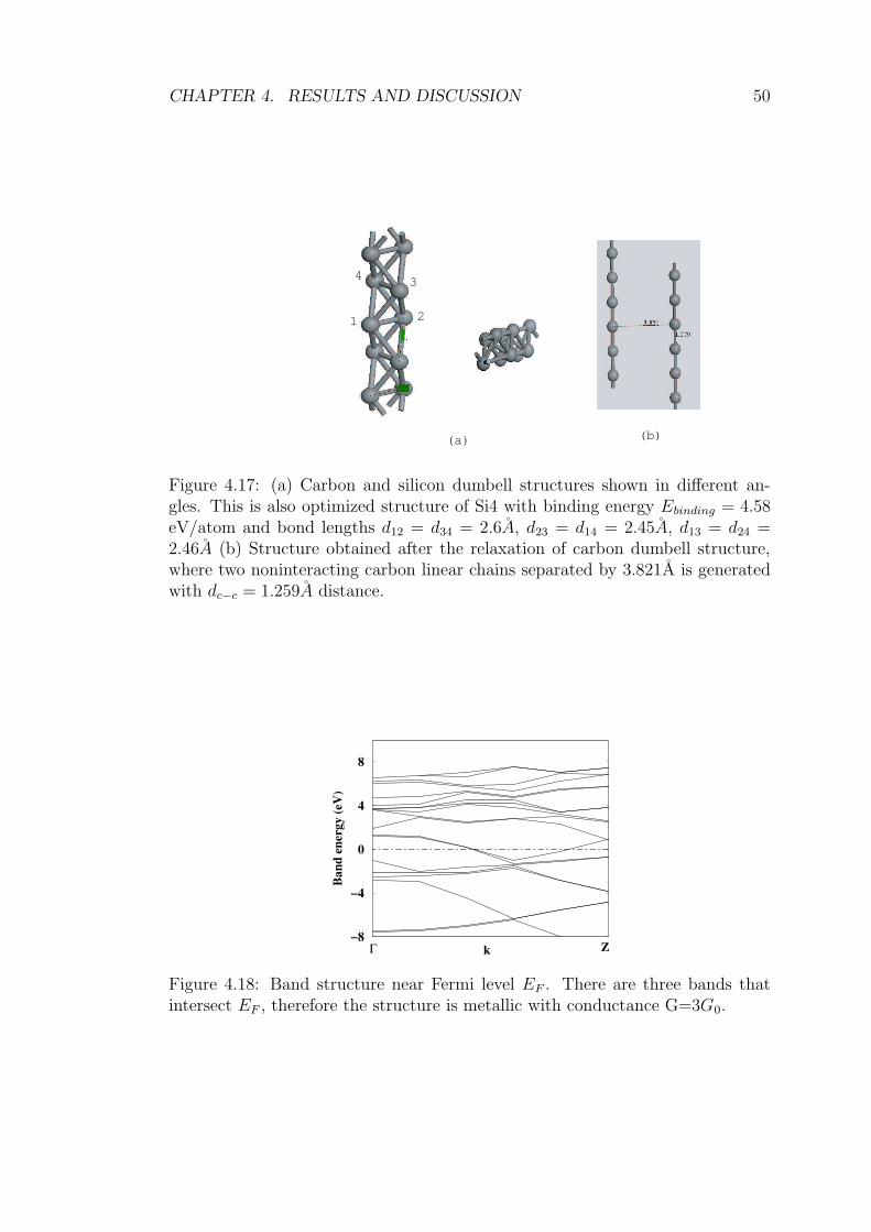
CHAPTER 4. RESULTS AND DISCUSSION 50
1 2
34
(a) (b)
Figure 4.17: (a) Carbon and silicon dumbell structures shown in different an-gles. This is also optimized structure of Si4 with binding energy Ebinding = 4.58eV/atom and bond lengths d12 = d34 = 2.6A, d23 = d14 = 2.45A, d13 = d24 =2.46A (b) Structure obtained after the relaxation of carbon dumbell structure,where two noninteracting carbon linear chains separated by 3.821A is generatedwith dc−c = 1.259A distance.
−8
−4
0
4
8
Ban
d en
ergy
(eV
)
k ZΓ
Figure 4.18: Band structure near Fermi level EF . There are three bands thatintersect EF , therefore the structure is metallic with conductance G=3G0.
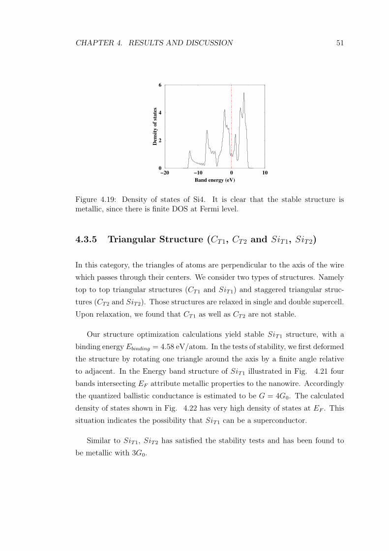
CHAPTER 4. RESULTS AND DISCUSSION 51
−20 −10 0 10Band energy (eV)
0
2
4
6
Den
sity
of s
tate
s
Figure 4.19: Density of states of Si4. It is clear that the stable structure ismetallic, since there is finite DOS at Fermi level.
4.3.5 Triangular Structure (CT1, CT2 and SiT1, SiT2)
In this category, the triangles of atoms are perpendicular to the axis of the wire
which passes through their centers. We consider two types of structures. Namely
top to top triangular structures (CT1 and SiT1) and staggered triangular struc-
tures (CT2 and SiT2). Those structures are relaxed in single and double supercell.
Upon relaxation, we found that CT1 as well as CT2 are not stable.
Our structure optimization calculations yield stable SiT1 structure, with a
binding energy Ebinding = 4.58 eV/atom. In the tests of stability, we first deformed
the structure by rotating one triangle around the axis by a finite angle relative
to adjacent. In the Energy band structure of SiT1 illustrated in Fig. 4.21 four
bands intersecting EF attribute metallic properties to the nanowire. Accordingly
the quantized ballistic conductance is estimated to be G = 4G0. The calculated
density of states shown in Fig. 4.22 has very high density of states at EF . This
situation indicates the possibility that SiT1 can be a superconductor.
Similar to SiT1, SiT2 has satisfied the stability tests and has been found to
be metallic with 3G0.
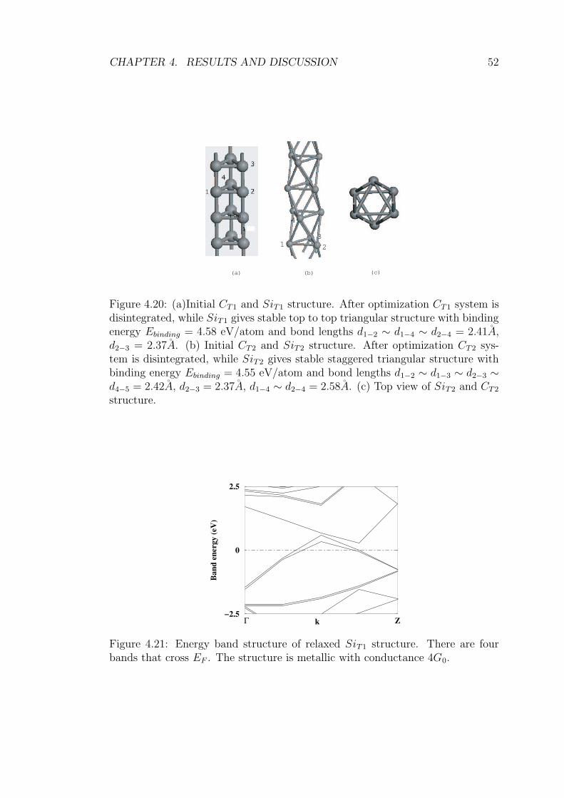
CHAPTER 4. RESULTS AND DISCUSSION 52
(a) (b) (c)
1 2
3
4
Figure 4.20: (a)Initial CT1 and SiT1 structure. After optimization CT1 system isdisintegrated, while SiT1 gives stable top to top triangular structure with bindingenergy Ebinding = 4.58 eV/atom and bond lengths d1−2 ∼ d1−4 ∼ d2−4 = 2.41A,d2−3 = 2.37A. (b) Initial CT2 and SiT2 structure. After optimization CT2 sys-tem is disintegrated, while SiT2 gives stable staggered triangular structure withbinding energy Ebinding = 4.55 eV/atom and bond lengths d1−2 ∼ d1−3 ∼ d2−3 ∼d4−5 = 2.42A, d2−3 = 2.37A, d1−4 ∼ d2−4 = 2.58A. (c) Top view of SiT2 and CT2
structure.
−2.5
0
2.5
Ban
d en
ergy
(eV
)
kΓ Z
Figure 4.21: Energy band structure of relaxed SiT1 structure. There are fourbands that cross EF . The structure is metallic with conductance 4G0.
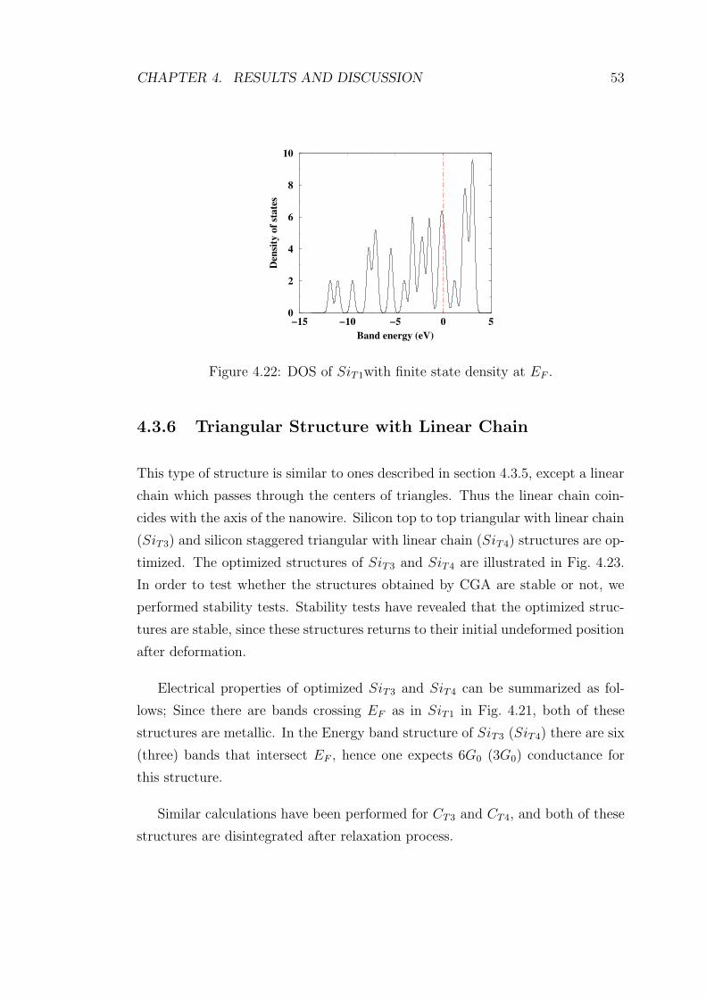
CHAPTER 4. RESULTS AND DISCUSSION 53
−15 −10 −5 0 5Band energy (eV)
0
2
4
6
8
10
Den
sity
of s
tate
s
Figure 4.22: DOS of SiT1with finite state density at EF .
4.3.6 Triangular Structure with Linear Chain
This type of structure is similar to ones described in section 4.3.5, except a linear
chain which passes through the centers of triangles. Thus the linear chain coin-
cides with the axis of the nanowire. Silicon top to top triangular with linear chain
(SiT3) and silicon staggered triangular with linear chain (SiT4) structures are op-
timized. The optimized structures of SiT3 and SiT4 are illustrated in Fig. 4.23.
In order to test whether the structures obtained by CGA are stable or not, we
performed stability tests. Stability tests have revealed that the optimized struc-
tures are stable, since these structures returns to their initial undeformed position
after deformation.
Electrical properties of optimized SiT3 and SiT4 can be summarized as fol-
lows; Since there are bands crossing EF as in SiT1 in Fig. 4.21, both of these
structures are metallic. In the Energy band structure of SiT3 (SiT4) there are six
(three) bands that intersect EF , hence one expects 6G0 (3G0) conductance for
this structure.
Similar calculations have been performed for CT3 and CT4, and both of these
structures are disintegrated after relaxation process.
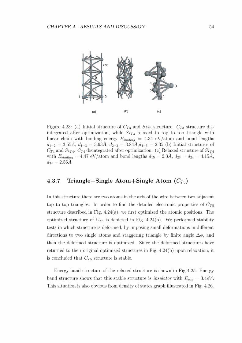
CHAPTER 4. RESULTS AND DISCUSSION 54
(a) (b)
1 23
4
12
34
5
(c)
5
2.35
Figure 4.23: (a) Initial structure of CT3 and SiT3 structure. CT3 structure dis-integrated after optimization, while SiT3 relaxed to top to top triangle withlinear chain with binding energy Ebinding = 4.34 eV/atom and bond lengthsd1−2 = 3.55A, d1−3 = 3.93A, d2−3 = 3.84A,d4−5 = 2.35 (b) Initial structures ofCT4 and SiT4. CT4 disintegrated after optimization. (c) Relaxed structure of SiT4
with Ebinding = 4.47 eV/atom and bond lengths d15 = 2.3A, d23 = d24 = 4.15A,d34 = 2.56A
4.3.7 Triangle+Single Atom+Single Atom (CT5)
In this structure there are two atoms in the axis of the wire between two adjacent
top to top triangles. In order to find the detailed electronic properties of CT5
structure described in Fig. 4.24(a), we first optimized the atomic positions. The
optimized structure of CT5 is depicted in Fig. 4.24(b). We performed stability
tests in which structure is deformed, by imposing small deformations in different
directions to two single atoms and staggering triangle by finite angle ∆φ, and
then the deformed structure is optimized. Since the deformed structures have
returned to their original optimized structures in Fig. 4.24(b) upon relaxation, it
is concluded that CT5 structure is stable.
Energy band structure of the relaxed structure is shown in Fig 4.25. Energy
band structure shows that this stable structure is insulator with Egap = 3.4eV .
This situation is also obvious from density of states graph illustrated in Fig. 4.26.

CHAPTER 4. RESULTS AND DISCUSSION 55
Figure 4.24: (a) Initial CT5 structure. (b) Relaxed CT5 structure with Ebinding =7.42 eV/atom and bond lengths d12 = 1.80A, d13 = 1.47A, d34 = 1.46A.
1 0
5
0
5
10
Ene
rgy
(eV
)
ZG
Figure 4.25: Energy band structure of the CT5 structure. CT5 is insulator owingto huge band gap of Egap = 3.4eV .
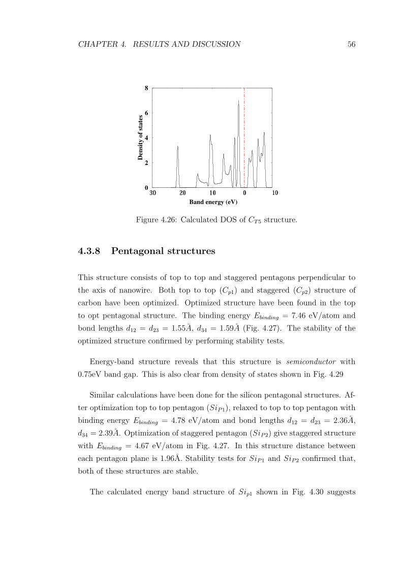
CHAPTER 4. RESULTS AND DISCUSSION 56
30 20 10 0 10Band energy (eV)
0
2
4
6
8
Den
sity
of s
tate
s
Figure 4.26: Calculated DOS of CT5 structure.
4.3.8 Pentagonal structures
This structure consists of top to top and staggered pentagons perpendicular to
the axis of nanowire. Both top to top (Cp1) and staggered (Cp2) structure of
carbon have been optimized. Optimized structure have been found in the top
to opt pentagonal structure. The binding energy Ebinding = 7.46 eV/atom and
bond lengths d12 = d23 = 1.55A, d34 = 1.59A (Fig. 4.27). The stability of the
optimized structure confirmed by performing stability tests.
Energy-band structure reveals that this structure is semiconductor with
0.75eV band gap. This is also clear from density of states shown in Fig. 4.29
Similar calculations have been done for the silicon pentagonal structures. Af-
ter optimization top to top pentagon (SiP1), relaxed to top to top pentagon with
binding energy Ebinding = 4.78 eV/atom and bond lengths d12 = d23 = 2.36A,
d34 = 2.39A. Optimization of staggered pentagon (SiP2) give staggered structure
with Ebinding = 4.67 eV/atom in Fig. 4.27. In this structure distance between
each pentagon plane is 1.96A. Stability tests for SiP1 and SiP2 confirmed that,
both of these structures are stable.
The calculated energy band structure of Sip1 shown in Fig. 4.30 suggests
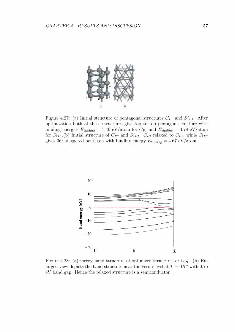
CHAPTER 4. RESULTS AND DISCUSSION 57
1 32
4
Figure 4.27: (a) Initial structure of pentagonal structures CP1 and SiP1. Afteroptimization both of these structures give top to top pentagon structure withbinding energies Ebinding = 7.46 eV/atom for CP1 and Ebinding = 4.78 eV/atomfor SiP1.(b) Initial structure of CP2 and SiP2. CP2 relaxed to CP1, while SiP2
gives 36o staggered pentagon with binding energy Ebinding = 4.67 eV/atom
−30
−20
−10
0
10
20
Ban
d en
ergy
(eV
)
ZΓ k
Figure 4.28: (a)Energy band structure of optimized structures of CP1. (b) En-larged view depicts the band structure near the Fermi level at T = 0Ko with 0.75eV band gap. Hence the relaxed structure is a semiconductor

CHAPTER 4. RESULTS AND DISCUSSION 58
3 0 20 1 0 0 10 20Energy (eV)
0
1
2
3
4
5
Den
sity
of S
tate
s
Figure 4.29: Density of states of relaxed structure of CP1. State density vanishesat EF .
−5
0
5
Ban
d en
ergy
(eV
)
ZΓ
Figure 4.30: Energy band structure of SiP1 structure. There are four bandscrossing the Fermi level EF .
metallic properties. Since there are four bands intersecting EF the conductance
of this structure is expected to be 4G0. Band structure and density of states of
SiP2 structure is similar to that of SiP1 except that there are three bands crossing
the Fermi level instead of four and state density at Fermi level is less than the
value for SiP2 at EF .

CHAPTER 4. RESULTS AND DISCUSSION 59
−15 −10 −5 0 5Energy (eV)
0
2
4
6
8
10
Den
sity
of S
tate
s
Figure 4.31: Total density of states for SiP1 structure. Finite density of states atFermi level indicates that the structure is metallic.
4.3.9 Pentagonal Structures with Linear Chain
This structure differs from the pentagonal structure in the previous section by the
inclusion of atomic chain (having single atom between the pentagons) coinciding
with the axis of the wire.
Silicon top to top pentagon with linear chain structure (SiP3) and staggered
pentagon with linear chain (SiP4) structures are described in Fig. 4.32. The latter
structure consists of two staggered pentagons where one pentagon is rotated by an
angle φ = 36o with respect to the other pentagon in the supercell and one single
atom placed between these two pentagon. Upon optimization we found that both
structures SiP3 and SiP4 are stable with binding energy Ebinding = 4.65eV and
Ebinding = 4.60eV respectively.
Electronic properties of SiP3 and SiP4 are comparable to that of SiP1. Since
there are six bands crossing the Fermi level for SiP3 and four bands for SiP4,
these structures are metallic with 6G0 and 4G0 conductance values. Energy band
structures and density of states are similar to that of SiP1 structure shown by
Fig. 4.30 and Fig. 4.31. CP3 and CP4 are disintegrated after optimization.
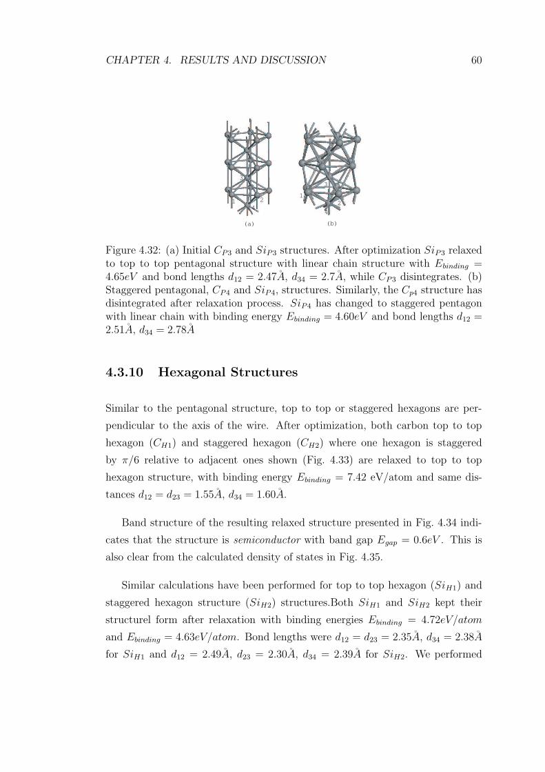
CHAPTER 4. RESULTS AND DISCUSSION 60
(a) (b)
1 2
3
4
12
3
4
Figure 4.32: (a) Initial CP3 and SiP3 structures. After optimization SiP3 relaxedto top to top pentagonal structure with linear chain structure with Ebinding =4.65eV and bond lengths d12 = 2.47A, d34 = 2.7A, while CP3 disintegrates. (b)Staggered pentagonal, CP4 and SiP4, structures. Similarly, the Cp4 structure hasdisintegrated after relaxation process. SiP4 has changed to staggered pentagonwith linear chain with binding energy Ebinding = 4.60eV and bond lengths d12 =2.51A, d34 = 2.78A
4.3.10 Hexagonal Structures
Similar to the pentagonal structure, top to top or staggered hexagons are per-
pendicular to the axis of the wire. After optimization, both carbon top to top
hexagon (CH1) and staggered hexagon (CH2) where one hexagon is staggered
by π/6 relative to adjacent ones shown (Fig. 4.33) are relaxed to top to top
hexagon structure, with binding energy Ebinding = 7.42 eV/atom and same dis-
tances d12 = d23 = 1.55A, d34 = 1.60A.
Band structure of the resulting relaxed structure presented in Fig. 4.34 indi-
cates that the structure is semiconductor with band gap Egap = 0.6eV . This is
also clear from the calculated density of states in Fig. 4.35.
Similar calculations have been performed for top to top hexagon (SiH1) and
staggered hexagon structure (SiH2) structures.Both SiH1 and SiH2 kept their
structurel form after relaxation with binding energies Ebinding = 4.72eV/atom
and Ebinding = 4.63eV/atom. Bond lengths were d12 = d23 = 2.35A, d34 = 2.38A
for SiH1 and d12 = 2.49A, d23 = 2.30A, d34 = 2.39A for SiH2. We performed
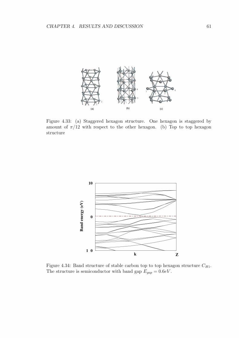
CHAPTER 4. RESULTS AND DISCUSSION 61
(a) (b)
1 2
3
4
13
2
(c)
12 3
4
Figure 4.33: (a) Staggered hexagon structure. One hexagon is staggered byamount of π/12 with respect to the other hexagon. (b) Top to top hexagonstructure
1 0
0
10
Ban
d en
ergy
(eV
)
ZG k
Figure 4.34: Band structure of stable carbon top to top hexagon structure CH1.The structure is semiconductor with band gap Egap = 0.6eV .
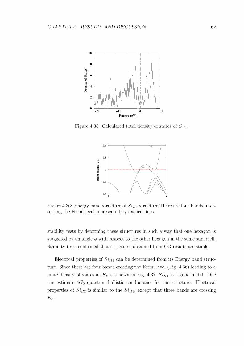
CHAPTER 4. RESULTS AND DISCUSSION 62
2 0 10 0 10Energy (eV)
0
2
4
6
8
10
Den
sity
of S
tate
s
Figure 4.35: Calculated total density of states of CH1.
−0.6
−0.3
0
0.3
0.6
Ban
d en
ergy
(eV
)
ZΓ
Figure 4.36: Energy band structure of SiH1 structure.There are four bands inter-secting the Fermi level represented by dashed lines.
stability tests by deforming these structures in such a way that one hexagon is
staggered by an angle φ with respect to the other hexagon in the same supercell.
Stability tests confirmed that structures obtained from CG results are stable.
Electrical properties of SiH1 can be determined from its Energy band struc-
ture. Since there are four bands crossing the Fermi level (Fig. 4.36) leading to a
finite density of states at EF as shown in Fig. 4.37, SiH1 is a good metal. One
can estimate 4G0 quantum ballistic conductance for the structure. Electrical
properties of SiH2 is similar to the SiH1, except that three bands are crossing
EF .

CHAPTER 4. RESULTS AND DISCUSSION 63
−15 −10 −5 0 5Energy (eV)
0
5
10
15
Den
sity
of S
tate
s
Figure 4.37: Calculated density of states (DOS) of SiH1.
4.3.11 Hexagonal Structures with Linear Chain
This structure is similar to hexagonal structures in the previous section, except
that an axial atomic chain, passes through the centers of hexagons. First we con-
sider silicon top to top hexagon with linear chain (SiH3) and staggered hexagon
with linear chain (SiH4). Upon optimizing SiH3 (SiH4) remained top to top
(staggered) hexagon with binding energy Ebinding = 4.75eV (Ebinding = 4.65eV )
and bond distances d12 = 2.35A (d12 = d25 = 2.48A, d34 = 2.3A). Stability tests
have shown that SiH3 and SiH4 structures are stable.
Energy band structure and DOS of SiH3 and SiH4 are similar to that of SiH1
structure. Both structures are metallic with 6G0 for SiH4 and 4G0 conductance
for SiH3 structure.
Similar calculations were performed for carbon top to top hexagon with lin-
ear chain (CH3) and carbon staggered hexagon with linear chain (CH4). After
relaxation, both of these structures are disintegrated.

CHAPTER 4. RESULTS AND DISCUSSION 64
4.3.12 Hexagon+Hexagon+Triangle Structure (CH5 and
SiH5)
This structure consists of two hexagons and one triangle and is reminiscent of a
diamond along the [111] direction. Optimized carbon hexagon+hexagon+triangle
structure (CH5) is stable and has binding energy Ebinding = 7.42 eV/atom. Band
structure of the optimized stable structure is illustrated in Fig. 4.40. Since there is
one two-fold degenerate band that intersects EF , stable CH5 structure is metallic,
this is also clear from the calculated DOS in Fig. 4.41. From the number of bands
that intersect Fermi level, one can predict that quantum ballistic conductance of
the system is 2G0.
Similar optimization calculations on silicon hexagon+hexagon+triangle
(SiH5) structure, resulted in disintegration.
Figure 4.38: (a) Staggered hexagon with linear chain structure where one hexagonis rotated in its plane by an angle φ = 30o relative to the adjacent hexagons. (b)Top to top hexagon with linear chain structure.
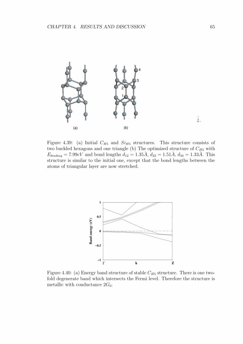
CHAPTER 4. RESULTS AND DISCUSSION 65
(a) (b)
1
2
3
4
Figure 4.39: (a) Initial CH5 and SiH5 structures. This structure consists oftwo buckled hexagons and one triangle (b) The optimized structure of CH5 withEbinding = 7.99eV and bond lengths d12 = 1.35A, d23 = 1.51A, d34 = 1.33A. Thisstructure is similar to the initial one, except that the bond lengths between theatoms of triangular layer are now stretched.
−1
−0.5
0
0.5
1
Ban
d en
ergy
(eV
)
ZΓ k
Figure 4.40: (a) Energy band structure of stable CH5 structure. There is one two-fold degenerate band which intersects the Fermi level. Therefore the structure ismetallic with conductance 2G0.

CHAPTER 4. RESULTS AND DISCUSSION 66
−20 −10 0 10Energy (eV)
0
2
4
6
8
10
Den
sity
of S
tate
s
Figure 4.41: Calculated DOS of CH5
4.3.13 Buckled Hexagon and Triangle Based Structure(CH6
and SiH6)
This structure consists of two triangle where one triangle 180o staggered with
respect to the other triangle and two buckled hexagon. Each buckled hexagon
structure can be envisioned as composed of two 180o staggered triangle with a
0.51A spacing. Carbon triangle+ buckled hexagon+staggered triangle+buckled
hexagon structure CH6 in Fig. 4.42 (a) is relaxed. The optimized structure of
CH6 is depicted in Fig. 4.42 (b), with binding energy Ebinding = 7.93 eV/atom.
The stability tests of the CH6 structure is further performed by displacing atoms
from equilibrium positions. Upon relaxing displaced atoms have returned to their
original positions.
Electronic properties of this stable structure are summarized in Fig. 4.43.
Calculated band structure and density of states indicate that this structure is
metallic. We can estimate conductance of the stable structure near Fermi level
from the number of crossing bands. Since there are three bands that intersect
Fermi level, we can say that the conductance of the structure 3G0. Similar
calculations carried out for silicon triangle+buckled hexagon+staggered trian-
gle+buckled hexagon structure (SiH6) have resulted in instable structure.
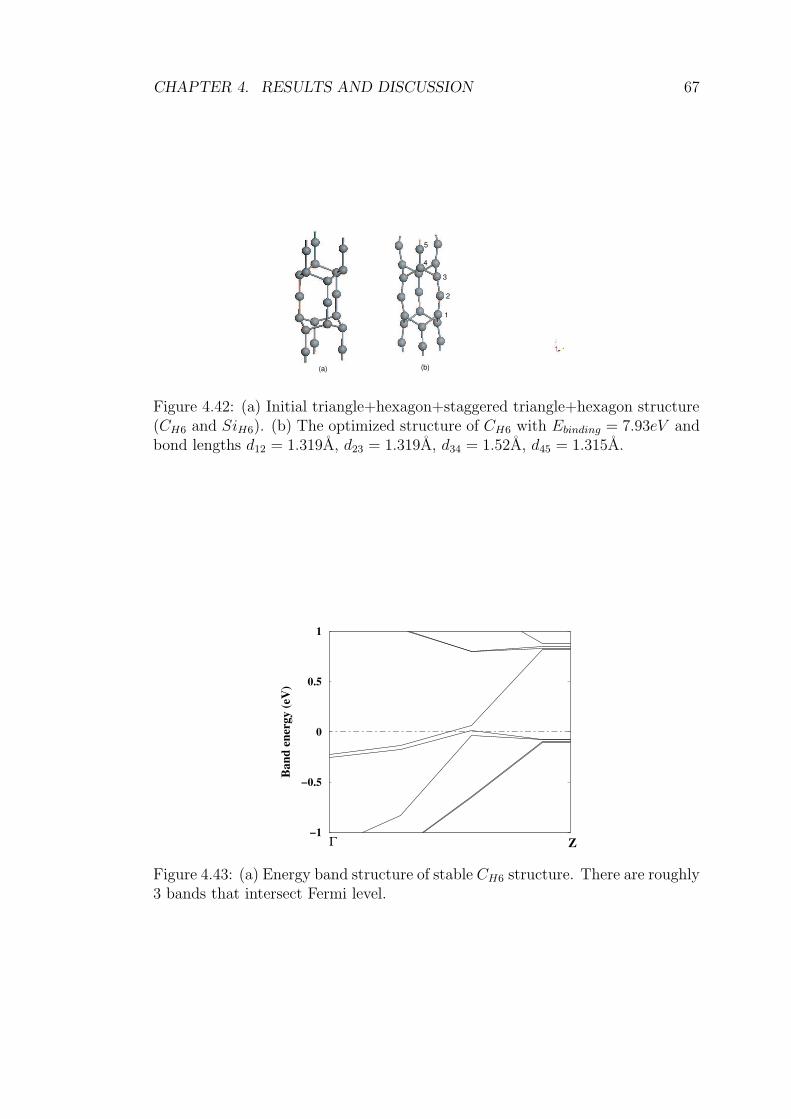
CHAPTER 4. RESULTS AND DISCUSSION 67
(a) (b)
1
2
3
4
5
Figure 4.42: (a) Initial triangle+hexagon+staggered triangle+hexagon structure(CH6 and SiH6). (b) The optimized structure of CH6 with Ebinding = 7.93eV andbond lengths d12 = 1.319A, d23 = 1.319A, d34 = 1.52A, d45 = 1.315A.
−1
−0.5
0
0.5
1
Ban
d en
ergy
(eV
)
ZΓ
Figure 4.43: (a) Energy band structure of stable CH6 structure. There are roughly3 bands that intersect Fermi level.

CHAPTER 4. RESULTS AND DISCUSSION 68
−20 −10 0Energy (eV)
0
5
10
15
Den
sity
of S
tate
s
Figure 4.44: Calculated DOS of stable CH6 structure.
4.3.14 Silicon Nanotubes
Tubes are another class of structure for one-dimensional nanowires. In the past
decade several novel properties of carbon nanotubes have been investigated ac-
tively. These properties have been used to make prototypes of various nanoscale
electronic devices. In this thesis, we do not involve with the physical properties
of carbon nanotubes. On the other hand Si being in the same IV column as C
atom, has similar crystal structure. It is of intent to know whether Si has stable
tubular structures.
Silicon (8,0) nanotubes is optimized by using 7 k-points and 300 eV energy
cutoff value with supercell lattice parameters as = bs = 20 Aand cs = c = 6.67 A.
Optimization carried out by CG on the (8,0) tube yields binding energy Ebinding =
4.80 eV/atom (Etotal = −3455.88eV ). The relaxed structure is illustrated in
Fig. 4.45.
Electrical properties of relaxed (8,0) tube are investigated by analyzing the
calculated energy band structure in Fig. 4.46. We found silicon zigzag (8,0) tube
is metallic with G = 3G0 due to three bands intersecting the Fermi level.
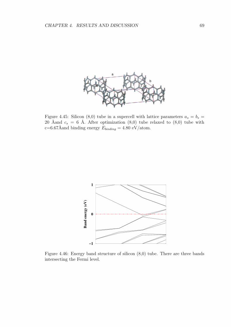
CHAPTER 4. RESULTS AND DISCUSSION 69
a
bc
Figure 4.45: Silicon (8,0) tube in a supercell with lattice parameters as = bs =20 Aand cs = 6 A. After optimization (8,0) tube relaxed to (8,0) tube withc=6.67Aand binding energy Ebinding = 4.80 eV/atom.
−1
0
1
Ban
d en
ergy
(eV
)
Figure 4.46: Energy band structure of silicon (8,0) tube. There are three bandsintersecting the Fermi level.
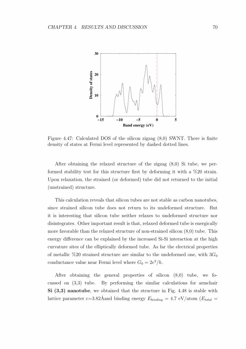
CHAPTER 4. RESULTS AND DISCUSSION 70
−15 −10 −5 0 5Band energy (eV)
0
10
20
30
Den
sity
of s
tate
s
Figure 4.47: Calculated DOS of the silicon zigzag (8,0) SWNT. There is finitedensity of states at Fermi level represented by dashed dotted lines.
After obtaining the relaxed structure of the zigzag (8,0) Si tube, we per-
formed stability test for this structure first by deforming it with a %20 strain.
Upon relaxation, the strained (or deformed) tube did not returned to the initial
(unstrained) structure.
This calculation reveals that silicon tubes are not stable as carbon nanotubes,
since strained silicon tube does not return to its undeformed structure. But
it is interesting that silicon tube neither relaxes to undeformed structure nor
disintegrates. Other important result is that, relaxed deformed tube is energically
more favorable than the relaxed structure of non-strained silicon (8,0) tube. This
energy difference can be explained by the increased Si-Si interaction at the high
curvature sites of the elliptically deformed tube. As far the electrical properties
of metallic %20 strained structure are similar to the undeformed one, with 3G0
conductance value near Fermi level where G0 = 2e2/h.
After obtaining the general properties of silicon (8,0) tube, we fo-
cussed on (3,3) tube. By performing the similar calculations for armchair
Si (3,3) nanotube, we obtained that the structure in Fig. 4.48 is stable with
lattice parameter c=3.82Aand binding energy Ebinding = 4.7 eV/atom (Etotal =

CHAPTER 4. RESULTS AND DISCUSSION 71
Figure 4.48: Relaxed structure of armchair silicon (3,3) nanotube. withc=3.82Aand binding energy Ebinding = 4.7 eV/atom.
−1294.66eV ).
By analyzing Band structure of silicon (3,3) tube, we concluded that the
relaxed structure is metallic with 2G0 conductance.
We performed stability tests for silicon (3,3) tube, by deforming the struc-
ture in radial direction by amount of %5,%10 and %15. After relaxation, we
observed that these structures return to the %5,%10 and %15 strained struc-
tures with total energies Etotal5 = −1294.61eV , Etotal10 = −1294.60eV and
Etotal15 = −1294.54eV . By analyzing these energy values, we concluded that
the non-strained silicon (3,3) tube is the most stable structure, but it should be
noted that there is not much energy difference between these strained tubes.
Electrical properties of these structures are similar to that of silicon (3,3)
tube, except that %15 strained (3,3) tube has 3G0 conductance value instead of
2G0 for other structures.
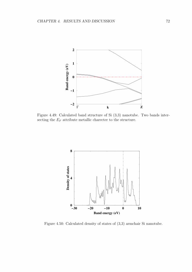
CHAPTER 4. RESULTS AND DISCUSSION 72
−2
−1
0
1
2
Ban
d en
ergy
(eV
)
k ZΓ
Figure 4.49: Calculated band structure of Si (3,3) nanotube. Two bands inter-secting the EF attribute metallic charecter to the structure.
−30 −20 −10 0 10Band energy (eV)
0
4
8
Den
sity
of s
tate
s
Figure 4.50: Calculated density of states of (3,3) armchair Si nanotube.
CHAPTER 4. RESULTS AND DISCUSSION 73
4.4 Conclusions and Future Work
4.4.1 Conclusions
Our work reveals a number of interesting physical properties of different types of
silicon and carbon nanowires which are explained in the previous chapter. We
believe that these findings are essential for future development of nanoelectronics
design both experimentally and theoretically. The structures by themselves are
important and essential to understand 1-D periodicity, namely crystallography
in one-dimension. Now, we highlight some of the important findings by way of
conclusion:
1. Carbon linear chain structure is the most stable structure among other
stable carbon nanowires with binding energy Ebinding = 8.29eV/atom which is
comparable with the cohesive energy of bulk carbon in diamond structure with
Ebinding ' 8.43eV (Fig. 4.51).
The stability of the carbon chain atoms stems from the two-fold π-bonds
formed by carbon 2px and 2py orbitals, and also σ-bond made from carbon 2s+2pz
orbitals. As compared to the tetrahedrally bonded diamond, bonds in the linear
chain are stronger and charge is more localized along the C-C bands. We specify
the bond as double bond. This explains also why the cohesive energy of the carbon
linear chain is comparable to the bulk diamond, in spite of the reduced nearest
neighbor interaction (2 in chain, 4 in diamond) Interestingly, other structures,
such as C2, C3 and C4, have changed to linear structure upon relaxation. In
spite of the fact that diamond is an insulator with band gap ∼5.4 eV, the chain
structure is metallic with quantum ballistic conductance G=2G0. It is interesting
to note that the conductance of carbon linear chain is twice larger than that of
the gold linear chain.
Carbon linear chains have been fabricated in the center of carbon multiwall
nanotubes (MWNT). The high stability of the carbon linear chain revealed in this
thesis suggest that one can also obtain stable suspended carbon linear chains. One
contemplates that stretching of SWNTs can give rise to linear chains.
CHAPTER 4. RESULTS AND DISCUSSION 74
We found that Si also form stable linear chain structure which exhibits physical
properties similar to that of the carbon linear chain. It is metallic and has
quantum ballistic conductance of 2G0. Si linear chains have not been synthesized
yet. This work indicates that the fabrication of double bonded Si linear chain can
lead to important applications, in particular as a interconnects in the Si-based
microelectronics where device size is rapidly reducing to 20-30 nanometers.
Simple nanowire structures, which are similar to linear chain are zigzag and
triangular structures can be formed by Si, but these structures are not stable in
carbon. It has been shown that these structures are stable also in metals such
as Al and Au. The instability of these structures in carbon are attributed to
the absence of sizeable core electron density. We found that Si nanowires having
triangular or zigzag structure are good conductors.
3. Some of the carbon nanowires from CT1 to CH6 has been disintegrated after
optimization while others give stable structure with binding energy less than that
of linear chain (C1). But it should be noted that, binding energy of CH5 and CH6
is still close to the bulk carbon binding energy and these structures are metallic.
4. None of the silicon nanowires has been disintegrated after optimization by
using first-principle pseudopotential. Hence, we concluded that silicon element is
possibly very suitable material for interconnection.
5. As described in detail in the previous section, we revealed a number of
interesting nanowire structures; some of them stable in Si, some of them in C or
in both elements. Some structures are metal, some are semiconductor. This work
is opening a new field which is full of novel physical properties.
4.4.2 Future Work
Our more systematic study of stability using temperature dependent quantum
molecular dynamics (QMD) and calculation of phonon spectrum is in progress.
In fact, stability of the structure, such as linear chain have been tested by QMD
and phonon density calculations.
CHAPTER 4. RESULTS AND DISCUSSION 75
We also performed first-principle calculations of transmission coefficient based
on the Keldysh non-equilibrium quantum statistical mechanics. We plan to per-
form similar calculation for wires suspended between two electrodes.
We plan to extend our study for composite wires made by metal and Si (C)
atoms, and calculate their magnetic properties. The magnetic ground state of
these wires can be important for spintronics.
4.4.3 General Remarks
Based on the first-principles pseudopotential plane wave calculations, we showed
that most of the Si and C based nanowires are metallic despite their parent bulk
crystals are semiconductor or insulator and strongly directed bonds. In fact, Si
and C being group IV elements have (ns)2 and (np)2 valance structure. One of the
valance s-orbitals are promoted to p-state, and finally (ns)1 (np)3 valance orbital
form four tetrahedrally directed (sp)3 orbitals. These hybrid orbitals, in turn,
form covalent bonds with nearest neighbor atoms. The crystal structure which
is formed at the end is specified as diamond structure; it is an open structure
but relatively strong owing to these directed bonds. Since number of electrons
stored to each band are even, and also conduction bands do not overlap with the
valance band, a finite band gap (1.1 eV for Si and 5.4 eV for diamond) forms
between them. In nanowires, one faces a different situation, where the banding
may be different from the tetrahedral coordination as far as number of bands and
their directions are concerned. In the case of linear chain, each atom has two
nearest neighbors and cylindrical symmetry. Then the atomic orbitals are forced
to form double bands. Because of the cylindrical symmetry around the axis of
the chain and valency of the atoms, the chain is metallic, and has conductance
two times higher than the conductance of gold chain. The situation may be
different for the nanowires which have coordination number higher that four.
For certain pentagonal and hexagonal structures the number of nearest neighbor
can be much larger than four, where the character of the bonds is remarkably
different. As far the question, whether the bonding can be stable in spite of thee
higher coordination can be sought in the 3D crystal structure of these elements
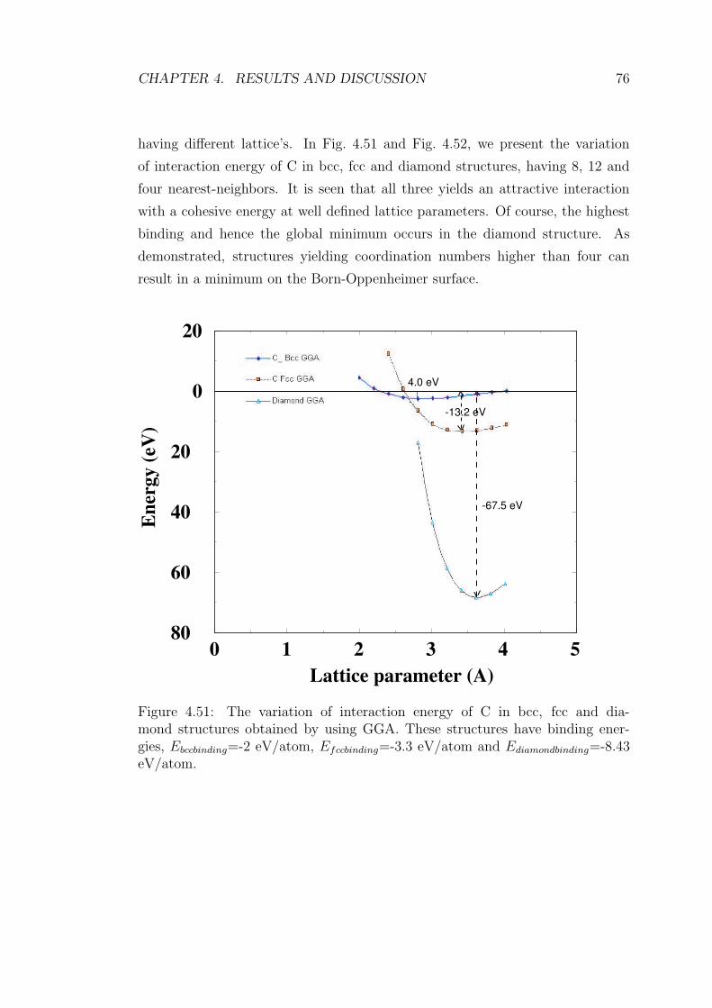
CHAPTER 4. RESULTS AND DISCUSSION 76
having different lattice’s. In Fig. 4.51 and Fig. 4.52, we present the variation
of interaction energy of C in bcc, fcc and diamond structures, having 8, 12 and
four nearest-neighbors. It is seen that all three yields an attractive interaction
with a cohesive energy at well defined lattice parameters. Of course, the highest
binding and hence the global minimum occurs in the diamond structure. As
demonstrated, structures yielding coordination numbers higher than four can
result in a minimum on the Born-Oppenheimer surface.
0 1 2 3 4 5Lattice parameter (A)
80
60
40
20
0
20
Ene
rgy
(eV
)
-67.5 eV
-13.2 eV
4.0 eV
Figure 4.51: The variation of interaction energy of C in bcc, fcc and dia-mond structures obtained by using GGA. These structures have binding ener-gies, Ebccbinding=-2 eV/atom, Efccbinding=-3.3 eV/atom and Ediamondbinding=-8.43eV/atom.
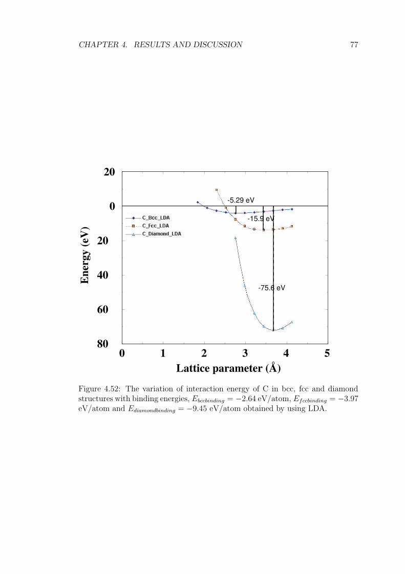
CHAPTER 4. RESULTS AND DISCUSSION 77
0 1 2 3 4 5Lattice parameter (A)
80
60
40
20
0
20
Ene
rgy
(eV
)
-5.29 eV
-15.9 eV
-75.6 eV
o
Figure 4.52: The variation of interaction energy of C in bcc, fcc and diamondstructures with binding energies, Ebccbinding = −2.64 eV/atom, Efccbinding = −3.97eV/atom and Ediamondbinding = −9.45 eV/atom obtained by using LDA.

Bibliography
78
Bibliography
[1] H. Ohnishi, Y.Kondo and KK.Takayanagi, Nature 395,780 (1998)
[2] A.I.Yanson, G.R Bolliger, H.E. Van der Brom, N.Agrait and J.M. van
Ruitenbeek, Nature 395,783 (1998)
[3] P.Sen, O.Gulseren, T.Yildirim, I.P.Batra and S.Ciraci Phys Rev. B 64,
195420 (2001)
[4] S. Iijima, Nature 354, 56 (1991)
[5] D. S. Bethune, C. H. Kiang, M. S. de Vries, G. Gorman, R. Savoy, J.
Vazquez and R. Beyers, Nature 363, 605 (1993).
[6] S. Iijima and T. Ichihashi, Nature 363, 603 (1993).
[7] A. Thess, R. Lee, P. Nikolaev, H. Dai, P. Petit, J. Robert, C. Xu, Y. H.
Lee, S. G. Kim, A. G. Rinzler, D. T. Colbert, G. E. Scuseria, D.Tomanek,
J. E. Fischer, and R. E. Smalley, Science 273, 483 (1996).
[8] G.Dresselhaus, Ph.Avouris; Carbon Nanotubes Springer (2001)
[9] E.Durgun, S.Dag ,S.Ciraci and O.Gulseren Journal of Physical Chem. (To
be published) (2003)
[10] S.Dag, E.Durgun and S.Ciraci Phys. Rev.B, Rapid Com. To be Published
(2003)
[11] Stefan Frank et al., Science 280 1744 (1998)
79

BIBLIOGRAPHY 80
[12] Hyoung Joon Choi,Jisoon Ihm,Young-Gui Yoon and Steven G. Louie Phys-
ical Review B Volume 60, 14009 (1999)
[13] Mehrez H, Ciraci S, Buldum A and Batra I P 1997 Phys. Rev. B 55 R1981
[14] Scheer E et al 1998 Nature 394 154
[15] Lang N D 1997 Phys. Rev. Lett. 79 1357
[16] Kalmeyer V R and Laughlin R B 1987 Phys. Rev. B 35 9805
[17] Yanson A I, Bolliger G R, van der Brom H E, Agrat N and van Ruitenbeek
J M 1998 Nature 395 783
[18] Lang N D 1995 Phys. Rev. B 52 5335
[19] A.Buldum, S.Ciraci and C.Y.Fong J.Phys:Conds.Matter 12 3349-3358
(2000)
[20] Ozpineci A and Ciraci S 2001 Phys. Rev. B 63 125415
[21] M.Born and J.R Oppenheimer, Ann der Phys. 84,457 (1927)
[22] D.R.Hartree, Proc. Cambridge. Philos.Soc. 24, 89 (1928)
[23] V.Forc, Z.Phys. 61,126 (1930)
[24] J.C.Slater,Phys. 35, 210 (1930)
[25] L.H. Thomas, Proc. Cambridge. Philos.Soc. 24, 89 (1928)
[26] E.Fermi, Z.Phys. 48,73 (1928)
[27] P.Hohenberg and W.Kohn, Phys.Rev 136.B864 (1964)
[28] W.Kohn and L.J.Sham, Phys.Rev. 140,a1133 (1965)
[29] James C. Phillips Phys.Rev. 112 3, 685 (November 1958).
[30] James C. Phillips and Leonard Kleinman. Phys. Rev. 116 2, 287 (1959).
[31] Charles Kittel, Introduction to Solid State Physics, 7th edition

BIBLIOGRAPHY 81
[32] J. Ihm. Rep. Prog. Phys. 51 (1), 105 (1988).
[33] W. E. Pickett. Comp.Phys. Rep. 9 (3), 115 (1989).
[34] P.Fulde Electron Correlations in Molecules and Solids Springer-
Verlag,Berlin.(1993)
[35] J.Perdew Intl. J. Quant. Chem 57 309 (1996)
[36] D. R. Hamann Phys. Rev. Lett. 76 660 (1996)
[37] R.Landauer, Philos. Mag. 21, 863 (1970)
[38] S. Datta, Electronic Transport in Mesoscopic Systems Cambridge Univer-
sity Press, Cambridge, (1995)
[39] M.B.Nardelli Phys Rev.B Vol.60 7828
[40] Slater, Koster Phys. Rev B. Vol.17 2376
[41] W.A.Harrison, Electronic Structure and Properties of Solids, Freenman,
San Fransisco (1980)
[42] Phillips, Pandey Phys. Rev.B, 13, 750 (1976)
[43] C.H.Xu, C.Z.Wang, C.T. Chan and K.M.Ho Journal of Phys Cond. Matter,
Vol 4, 6047 (1992)
[44] N.W.Ashcroft, N.D.Mermin Solid State Physics, Sounders College Publish-
ing (1970)
[45] J.P.Perdew, J.A.Chevary, S.H.Vosko, K.A.Jackson, M.R.Pederson,
D.J.Singh and C.Fiolhois, Phys Rev.B 46, 6671 (1992)
[46] D.Vanderbilt, Phys. Rev. B 41, 7892 (1990)
[47] H.J.Monkhorst and J.D.Pack, Phys. Rev.B. 13,5188 (1976)