SiI3114 PCI to Serial ATA Controller Data Sheet - Pix · PCI to Serial ATA Controller Data Sheet...
127
SiI3114 PCI to Serial ATA Controller Data Sheet Document # SiI-DS-0103-D Data Sheet
Transcript of SiI3114 PCI to Serial ATA Controller Data Sheet - Pix · PCI to Serial ATA Controller Data Sheet...
SiI3114 PCI to Serial ATA Controller Data Sheet
Document # SiI-DS-0103-D
Data Sheet
SiI3114 PCI to Serial ATA Controller Data Sheet
Silicon Image, Inc.
SiI-DS-0103-D ii © 2007 Silicon Image, Inc.
February 2007
Copyright Notice Copyright © 2007 Silicon Image, Inc. All rights reserved. These materials contain proprietary and confidential information (including trade secrets, copyright and other interests) of Silicon Image, Inc. You may not use these materials except only for your bona fide non-commercial evaluation of your potential purchase of products and/services from Silicon Image or its affiliates, and/or only in connection with your purchase of products and/or services from Silicon Image or its affiliates, and only in accordance with the terms and conditions herein. You have no right to copy, modify, transfer, sublicense, publicly display, create derivative works of or distribute these materials, or otherwise make these materials available, in whole or in part, to any third party.
Trademark Acknowledgment Silicon Image™, VastLane™, SteelVine™, PinnaClear™, Simplay™, Simplay HD™, Satalink™, and TMDS™ are trademarks or registered trademarks of Silicon Image, Inc. in the United States and other countries. HDMI™, the HDMI logo and High-Definition Multimedia Interface™ are trademarks or registered trademarks of, and are used under license from, HDMI Licensing, LLC.
Further Information To request other materials, documentation, and information, contact your local Silicon Image, Inc. sales office or visit the Silicon Image, Inc. web site at www.siliconimage.com.
Revision History
© 2007 Silicon Image. Inc.
Revision Date Comment
A 09/08/03 Derived from Preliminary datasheet Rev 0.65. A1 10/16/03 Updated Table 2-6 SerDes Reference Clock Input Requirements; Updated Table 2-1 Absolute
Maximum Ratings; Corrected inconsistent sentences (minor fixes including mistyping) A2 10/30/03 Updated Section 8.2 Serial ATA Device Initialization A3 02/05/04 Corrected part number on cover page to SiI3114CT176 from SiI3114CT144 A4 04/05/05 Updated the part number on cover page to SiI3114 from SiI3114CT176; Added Part Ordering
Number in section 4. Package Drawing; Updated Marking Specification in section 4. Package Drawing
B 07/21/06 Corrected inconsistent sentences (minor fixes including mistyping); Updated SiI company logo C 11/29/06 This datasheet is no longer under NDA. Removed confidential markings D 02/23/07 New formatting applied throughout entire document.
SiI3114 PCI to Serial ATA Controller Data Sheet
Silicon Image, Inc.
© 2007 Silicon Image, Inc. iii SiI-DS-0103-D
Table of Contents Overview........................................................................................................................................................ 1
Key Benefits .............................................................................................................................................. 1 Features ..................................................................................................................................................... 1
Overall Features...................................................................................................................................... 1 PCI Features ........................................................................................................................................... 1 Serial ATA Features ................................................................................................................................. 1 Other Features ........................................................................................................................................ 2
Applications............................................................................................................................................... 2 References................................................................................................................................................. 2 Functional Description ............................................................................................................................. 2 PCI Interface .............................................................................................................................................. 2 PCI Initialization ........................................................................................................................................ 2 PCI Bus Operations .................................................................................................................................. 2 PCI Configuration Space.......................................................................................................................... 3 Deviations from the Specification........................................................................................................... 3
Electrical Characteristics............................................................................................................................. 4 Device Electrical Characteristics ............................................................................................................ 4 SATA Interface Timing Specifications..................................................................................................... 5 SATA Interface Transmitter Output Jitter Characteristics .................................................................... 6 CLKI SerDes Reference Clock Input Requirements.............................................................................. 6 PCI 33 MHz Timing Specifications .......................................................................................................... 6 PCI 66 MHz Timing Specifications .......................................................................................................... 7 Flash Memory Timing Specifications...................................................................................................... 7
Pin Definitions............................................................................................................................................... 8 SiI3114 Pin Listing.................................................................................................................................... 8 SiI3114 Pin Diagram ............................................................................................................................... 13 SiI3114 Pin Descriptions........................................................................................................................ 14
PCI 66MHz 32-bit .................................................................................................................................. 14 Miscellaneous I/O.................................................................................................................................. 16 Serial ATA Signals ................................................................................................................................. 17
Package Drawing........................................................................................................................................ 19 Package Markings ...................................................................................................................................... 20 Block Diagram............................................................................................................................................. 21 Auto-Initialization ....................................................................................................................................... 22
Auto-Initialization from Flash ................................................................................................................ 22 Auto-Initialization from EEPROM .......................................................................................................... 23
Register Definitions.................................................................................................................................... 25 PCI Configuration Space........................................................................................................................ 25
Device ID – Vendor ID........................................................................................................................... 26 PCI Status – PCI Command.................................................................................................................. 27 PCI Class Code – Revision ID .............................................................................................................. 28 BIST – Header Type – Latency Timer – Cache Line Size..................................................................... 28 Base Address Register 0....................................................................................................................... 29 Base Address Register 1....................................................................................................................... 29
SiI3114 PCI to Serial ATA Controller Data Sheet
Silicon Image, Inc.
SiI-DS-0103-D iv © 2007 Silicon Image, Inc.
Base Address Register 2....................................................................................................................... 29 Base Address Register 3....................................................................................................................... 30 Base Address Register 4....................................................................................................................... 30 Base Address Register 5....................................................................................................................... 30 Subsystem ID – Subsystem Vendor ID ................................................................................................. 31 Expansion ROM Base Address............................................................................................................. 31 Capabilities Pointer ............................................................................................................................... 32 Max Latency – Min Grant – Interrupt Pin – Interrupt Line ..................................................................... 32 Configuration ......................................................................................................................................... 32 Software Data Register ......................................................................................................................... 33 Power Management Capabilities .......................................................................................................... 33 Power Management Control + Status ................................................................................................... 34 PCI Bus Master – Channel 0/2.............................................................................................................. 34 PRD Table Address – Channel 0/2........................................................................................................ 35 PCI Bus Master – Channel 1/3.............................................................................................................. 35 PRD Table Address – Channel 1/3........................................................................................................ 35 Data Transfer Mode – Channel 0/2 ....................................................................................................... 36 Data Transfer Mode – Channel 1/3 ....................................................................................................... 36 System Configuration Status – Command ............................................................................................ 36 System Software Data Register ............................................................................................................ 37 Flash Memory Address – Command + Status....................................................................................... 37 Flash Memory Data ............................................................................................................................... 37 EEPROM Memory Address – Command + Status................................................................................ 38 EEPROM Memory Data ........................................................................................................................ 38 Channel 0/2 Task File Configuration + Status ....................................................................................... 38 Channel 1/3 Task File Configuration + Status ....................................................................................... 39 BA5 Indirect Address............................................................................................................................. 39 BA5 Indirect Access .............................................................................................................................. 39 Internal Register Space – Base Address 0 ........................................................................................... 40 Channel 0/2 Task File Register 0 .......................................................................................................... 40 Channel 0/2 Task File Register 1 .......................................................................................................... 40
Internal Register Space – Base Address 1 ........................................................................................... 41 Channel 0/2 Task File Register 2 .......................................................................................................... 41
Internal Register Space – Base Address 2 ........................................................................................... 42 Channel 1/3 Task File Register 0 .......................................................................................................... 42 Channel 1/3 Task File Register 1 .......................................................................................................... 42
Internal Register Space – Base Address 3 ........................................................................................... 43 Channel 1/3 Task File Register 2 .......................................................................................................... 43
Internal Register Space – Base Address 4 ........................................................................................... 44 PCI Bus Master – Channel 0/2.............................................................................................................. 44 PRD Table Address – Channel 0/2........................................................................................................ 44 PCI Bus Master – Channel 1/3.............................................................................................................. 45 PRD Table Address – Channel 1/3........................................................................................................ 45
Internal Register Space – Base Address 5 ........................................................................................... 46 PCI Bus Master – Channel X ................................................................................................................ 53 PRD Table Address – Channel X .......................................................................................................... 54 PCI Bus Master2 – Channel X .............................................................................................................. 54 Summary Interrupt Status...................................................................................................................... 56 PRD Address – Channel X .................................................................................................................... 56 PCI Bus Master Byte Count – Channel X ............................................................................................. 56 FIFO Valid Byte Count and Control – Channel X .................................................................................. 57 System Configuration Status – Command ............................................................................................ 57 System Software Data Register ............................................................................................................ 58 Flash Memory Address – Command + Status....................................................................................... 58 Flash Memory Data ............................................................................................................................... 59 EEPROM Memory Address – Command + Status................................................................................ 59 EEPROM Memory Data ........................................................................................................................ 60
SiI3114 PCI to Serial ATA Controller Data Sheet
Silicon Image, Inc.
© 2007 Silicon Image, Inc. v SiI-DS-0103-D
FIFO Port – Channel X.......................................................................................................................... 60 FIFO Pointers1– Channel X .................................................................................................................. 61 FIFO Pointers2– Channel X .................................................................................................................. 61 Channel X Task File Register 0 ............................................................................................................. 62 Channel X Task File Register 1 ............................................................................................................. 62 Channel X Task File Register 2 ............................................................................................................. 63 Channel X Read Ahead Data ................................................................................................................ 63 Channel X Task File Register 0 – Command Buffering......................................................................... 64 Channel X Task File Register 1 – Command Buffering......................................................................... 64 Channel X Extended Task File Register – Command Buffering ........................................................... 65 Channel X Virtual DMA/PIO Read Ahead Byte Count .......................................................................... 65 Channel X Task File Configuration + Status.......................................................................................... 65 Data Transfer Mode – Channel X.......................................................................................................... 66 Serial ATA SControl ............................................................................................................................... 67 Serial ATA SStatus................................................................................................................................. 68 Serial ATA SError................................................................................................................................... 69 Serial ATA SActive ................................................................................................................................. 70 SMisc..................................................................................................................................................... 70 Serial ATA PHY Configuration ............................................................................................................... 71 SIEN ...................................................................................................................................................... 72 SFISCfg ................................................................................................................................................. 73 RxFIS0-RxFIS6 ..................................................................................................................................... 73
Programming Sequences .......................................................................................................................... 74 Recommended Initialization Sequence for the SiI3114...................................................................... 74 Serial ATA Device Initialization .............................................................................................................. 75 Issue ATA Command............................................................................................................................... 76 PIO Mode Read/Write Operation............................................................................................................ 76 Watchdog Timer Operation.................................................................................................................... 77 PIO Mode Read Ahead Operation.......................................................................................................... 78 MDMA/UDMA Read/Write Operation ..................................................................................................... 78 Virtual DMA Read/Write Operation........................................................................................................ 79
Using Virtual DMA with Non-DMA Capable Devices............................................................................. 79 Using Virtual DMA with DMA Capable Devices..................................................................................... 81
Second PCI Bus Master Registers Usage ............................................................................................ 82 Power Management.................................................................................................................................... 83
Power Management Summary............................................................................................................... 83 Partial Power Management Mode.......................................................................................................... 83 Slumber Power Management Mode ...................................................................................................... 83 Hot Plug Support .................................................................................................................................... 84
FIS Support ................................................................................................................................................. 85 FIS Summary ........................................................................................................................................... 85 FIS Transmission .................................................................................................................................... 86 FIS Reception .......................................................................................................................................... 86 FIS Types Not Affiliated with Current ATA/ATAPI Operations ............................................................ 89
BIST Support ......................................................................................................................................... 89 BIST Signals.......................................................................................................................................... 89 DMA Setup ............................................................................................................................................ 89
SiI3114 PCI to Serial ATA Controller Data Sheet
Silicon Image, Inc.
SiI-DS-0103-D vi © 2007 Silicon Image, Inc.
ATA Command Decoding........................................................................................................................... 90 Data Modes .............................................................................................................................................. 90 ATA Commands....................................................................................................................................... 90
Obsolesced Commands........................................................................................................................ 92 Read/Write Long.................................................................................................................................... 92
Vendor Specific Command Support ..................................................................................................... 93 Silicon Image's Vendor Specific Commands......................................................................................... 93 Vendor Specific, Reserved, Retired and Obsolesced Commands ....................................................... 94 Definitions.............................................................................................................................................. 94 Scheme ................................................................................................................................................. 94
Bridge Device Vendor Specific Commands ......................................................................................... 96 Feature Set/Command Summary ......................................................................................................... 96 VS Lock ................................................................................................................................................. 97 VS Unlock Vendor Specific.................................................................................................................... 99 VS Unlock Reserved ........................................................................................................................... 101 VS Unlock Individual ........................................................................................................................... 103 VS Set General Protocol ..................................................................................................................... 105 VS Set Command Protocol ................................................................................................................. 107
State Transitions ................................................................................................................................... 109 Protocols Summary .............................................................................................................................. 112 Reading and Writing of Task File and Device Control Registers..................................................... 116
48-Bit LBA Addressing......................................................................................................................... 116 Device Control Register and Soft Reset ............................................................................................. 116
LED Support .......................................................................................................................................... 116 Flash and EEPROM Programming Sequences...................................................................................... 117
Flash Memory Access .......................................................................................................................... 117 PCI Direct Access................................................................................................................................ 117 Register Access................................................................................................................................... 117
EEPROM Memory Access .................................................................................................................... 118 EEPROM Write Operation................................................................................................................... 118 EEPROM Read Operation .................................................................................................................. 118
SiI3114 PCI to Serial ATA Controller Data Sheet
Silicon Image, Inc.
© 2007 Silicon Image, Inc. vii SiI-DS-0103-D
List of Figures Figure 1. Address Lines During Configuration Cycle ..................................................................................... 3 Figure 2. Flash Memory Timing...................................................................................................................... 7 Figure 3. SiI3114 Pin Diagram...................................................................................................................... 13 Figure 4. Package Drawing – 176 TQFP ..................................................................................................... 19 Figure 5. Marking Specification – SiI3114CT176 ......................................................................................... 20 Figure 6. Marking Specification – SiI3114CTU............................................................................................. 20 Figure 7. SiI3114 Block Diagram.................................................................................................................. 21 Figure 8. Auto-Initialization from Flash Timing ............................................................................................. 22 Figure 9. Auto-Initialization from EEPROM Timing....................................................................................... 23 Figure 10. Hot Plug Logic State Diagram..................................................................................................... 84
SiI3114 PCI to Serial ATA Controller Data Sheet
Silicon Image, Inc.
SiI-DS-0103-D viii © 2007 Silicon Image, Inc.
List of Tables Table 1. Absolute Maximum Ratings .............................................................................................................. 4 Table 2. DC Specifications.............................................................................................................................. 4 Table 3. SATA Interface DC Specifications..................................................................................................... 5 Table 4. SATA Interface Timing Specifications ............................................................................................... 5 Table 5. SATA Interface Transmitter Output Jitter Characteristics ................................................................. 6 Table 6. CLKI SerDes Reference Clock Input Requirements......................................................................... 6 Table 7. PCI 33 MHz Timing Specifications.................................................................................................... 6 Table 8. PCI 66 MHz Timing Specifications.................................................................................................... 7 Table 9. SiI3114 Pin Listing ............................................................................................................................ 8 Table 10. Pin Types ...................................................................................................................................... 12 Table 11. Auto-Initialization from Flash Timing ............................................................................................. 22 Table 12. Flash Data Description.................................................................................................................. 22 Table 13. Auto-Initialization from EEPROM Timing ...................................................................................... 23 Table 14. Auto-Initialization from EEPROM Timing Symbols ....................................................................... 23 Table 15. EEPROM Data Description........................................................................................................... 24 Table 16. SiI3114 PCI Configuration Space ................................................................................................. 25 Table 17. SiI3114 Internal Register Space – Base Address 0 ...................................................................... 40 Table 18. SiI3114 Internal Register Space – Base Address 1 ...................................................................... 41 Table 19. SiI3114 Internal Register Space – Base Address 2 ...................................................................... 42 Table 20. SiI3114 Internal Register Space – Base Address 3 ...................................................................... 43 Table 21. SiI3114 Internal Register Space – Base Address 4 ...................................................................... 44 Table 22. SiI3114 Internal Register Space – Base Address 5 ...................................................................... 46 Table 23. Software Data Byte, Base Address 5, Offset 00H ......................................................................... 53 Table 24. Software Data Byte, Base Address 5, Offset 10H ......................................................................... 55 Table 25. SError Register Bits (DIAG Field) ................................................................................................. 69 Table 26. SError Register Bits (ERR Field) .................................................................................................. 69 Table 27. Physical Region Descriptor (PRD) Format ................................................................................... 82 Table 28. Power Management Register Bits ................................................................................................ 83 Table 29. FIS Summary ................................................................................................................................ 85 Table 30. Configuration Bits for FIS Reception ............................................................................................ 86 Table 31. Default FIS Configurations............................................................................................................ 87 Table 32. ATA Commands Supported........................................................................................................... 90 Table 33. Data FIS ........................................................................................................................................ 93 Table 34. Vendor Specific Command Summary........................................................................................... 96 Table 35. 16-Entry Command Protocol Table............................................................................................. 108 Table 36. Registers Used When Issuing VS Set Command ...................................................................... 108 Table 37. Default State - VS_LOCKED ...................................................................................................... 109 Table 38. VS_VS......................................................................................................................................... 109 Table 39. VS_RSV...................................................................................................................................... 110 Table 40. VS_IND ....................................................................................................................................... 110 Table 41. VS_VS_RSV ............................................................................................................................... 110 Table 42. VS_VS_IND ................................................................................................................................ 110 Table 43. VS_RSV_IND...............................................................................................................................111 Table 44. VS_VS_RSV_IND........................................................................................................................111 Table 45. Protocol Code Encoding Scheme............................................................................................... 112 Table 46. Vendor Specific Protocol Code (in Alphabetical Order) .............................................................. 113 Table 47. Vendor Specific Protocol Code (by Protocol Code).................................................................... 114 Table 48. Vendor Specific Protocol Code (in Alphabetical Order) .............................................................. 115
SiI3114 PCI to Serial ATA Controller Data Sheet
© 2007 Silicon Image, Inc. SiI-DS-0103-D
Overview The Silicon Image SiI3114 is a single-chip solution for a PCI to Serial ATA controller. It accepts host commands through the PCI bus, processes them, and transfers data between the host and Serial ATA devices. It can be used to control four independent Serial ATA channels. Each channel has its own Serial ATA bus and will support one Serial ATA device. The SiI3114 supports a 32-bit 66 MHz PCI bus and the Serial ATA Generation 1 transfer rate of 1.5 Gbit/s (150 MB/s).
Key Benefits The Silicon Image SiI3114 PCI to Serial ATA Controller is the perfect single-chip solution for designs that need to accommodate storage peripherals with the new Serial ATA interface. Any system with a PCI bus interface can simply add the Serial ATA interface by adding a card with the SiI3114 and loading the driver into the system.
The SiI3114 comes complete with drivers for Windows 98, Windows Millennium, Windows NT 4.0, Windows 2000, XP, Windows 2003, Netware 5.1, 6.0, 6.5, Red Hat Linux 8.0, 9.0, SuSE Linux 8.1, 8.2 and United Linux 1.0.
Features Overall Features
• Standalone PCI to Serial ATA host controller chip • Compliant with PCI Specification, revision 2.3. • Compliant with Programming Interface for Bus Master IDE Controller, revision 1.0. • Driver support for Windows 98, Windows Millennium, Windows NT 4.0, Windows 2000, XP, Windows 2003,
Netware 5.1, 6.0, 6.5, Red Hat Linux 8.0, 9.0, SuSE Linux 8.1, 8.2 and United Linux 1.0 • Supports up to 4Mbit external Flash or EPROM for BIOS expansion. • Supports an external EEPROM, flash, or EPROM for programmable device ID, subsystem vendor ID,
subsystem product ID, and PCI sub-class code. • Supports the Silicon Image specific driver for special chip functions. • Fabricated in a 0.18μ CMOS process with a 1.8 volt core and 3.3 volt I/Os. • Supports Plug and Play. • Supports ATAPI device • Supports Activity LEDs, one for each channel with 12mA open drain driving capability. • Available in a 176-pin TQFP package.
PCI Features • Supports 66 MHz PCI with 32-bit data. • Supports PCI PERR and SERR reporting. • Supports PCI bus master operations: Memory Read, Memory Read Multiple, and Memory Write. • Supports PCI bus target operations: Configuration Read, Configuration Write, I/O Read, I/O Write, Memory
Read, Memory Write, Memory Read Line (Memory Read) and Memory Read Multiple (Memory Read) • Supports byte alignment for odd-byte PCI address access. • Supports jumper configurable PCI class code. • Supports programmable and EEPROM, Flash and EPROM loadable PCI class code. • Supports Base Address Register 5 in memory space.
Serial ATA Features • Integrated Serial ATA Link and PHY logic • Compliant with Serial ATA 1.0 specifications • Supports four independent Serial ATA channels. • Supports Serial ATA Generation 1 transfer rate of 1.5Gbit/s. • Supports Spread Spectrum in receiver • Single PLL architecture, 1 PLL for all four ports • Programmable drive strengths for Backplane applications
SiI3114 PCI to Serial ATA Controller Data Sheet
Silicon Image, Inc.
SiI-DS-0103-D 2 © 2007 Silicon Image, Inc.
Other Features • Features independent 256-byte FIFOs (32-bit x 64 deep) per Serial ATA channel for host reads and writes. • Supports legacy type operations (Master/Slave drive access) using I/O-mapped register space • Supports 4 concurrent operations using memory-mapped register space • Features Serial ATA to PCI interrupt masking. • Features Watch Dog Timer for fault resiliency. • Provides 8 bits of General Purpose I/O (GPIO)
Applications • PC motherboards • Serial ATA drive add on cards • Serial ATA RAID cards
References For more details about the Serial ATA technology, the reader is referred to the following industry specifications:
• Serial ATA / High Speed Serialized AT Attachment specification, Revision 1.0 • PCI Local Bus Specification Revision 2.3 • Advanced Power Management Specification Revision 1.0 • PCI IDE Controller Specification Revision 1.0 • Programming Interface for Bus Master IDE Controller, Revision 1.0
Functional Description The SiI3114 is a PCI-to-Serial ATA controller chip that transfers data between the PCI bus and storage media (e.g hard disk drive, etc). The SiI3114 consists of the following functional blocks:
• PCI Interface. Provides the interface to any system that has a PCI bus. Instructions and system clocks are based on this interface.
• Serial ATA Interface. Four separate channels to access storage media such as hard disk drive, floppy disk drive, CD-ROM.
PCI Interface The SiI3114 PCI interface is compliant with the PCI Local Bus Specification (Revision 2.3). The SiI3114 can act as a PCI master and a PCI slave, and contains the SiI3114 PCI configuration space and internal registers. When the SiI3114 needs to access shared memory, it becomes the bus master of the PCI bus and completes the memory cycle without external intervention. In the mode when it acts as a bridge between the PCI bus and the Serial ATA bus it will behave as a PCI slave.
PCI Initialization Generally, when a system initializes a module containing a PCI device, the configuration manager reads the configuration space of each PCI device on the PCI bus. Hardware signals select a specific PCI device based on a bus number, a slot number, and a function number. If a device that is addressed (via signal lines) responds to the configuration cycle by claiming the bus, then that function's configuration space is read out from the device during the cycle. Because any PCI device can be a multifunction device, every supported function's configuration space needs to be read from the device. Based on the information read, the configuration manager will assign system resources to each supported function within the device. Sometimes new information needs to be written into the function's configuration space. This is accomplished with a configuration write cycle.
PCI Bus Operations The SiI3114 behaves either as a PCI master or a PCI slave device at any time and switches between these modes as required during device operation. As a PCI slave, the SiI3114 responds to the following PCI bus operations:
• I/O Read • I/O Write
SiI3114 PCI to Serial ATA Controller Data Sheet
Silicon Image, Inc.
© 2007 Silicon Image, Inc. 3 SiI-DS-0103-D
• Configuration Read • Configuration Write • Memory Read • Memory Write
All other PCI cycles are ignored by the SiI3114.
As a PCI master, the SiI3114 generates the following PCI bus operations: • Memory Read Multiple • Memory Read • Memory Write
PCI Configuration Space This section describes how the SiI3114 implements the required PCI configuration register space. The intent of PCI configuration space definition is to provide an appropriate set of configuration registers that satisfy the needs of current and anticipated system configuration mechanisms, without specifying those mechanisms or otherwise placing constraints on their use. These registers allow for:
• Full device relocation (including interrupt binding) • Installation, configurations, and booting without user interventions • System address map construction by device-independent software
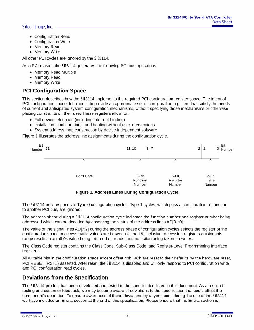
Figure 1 illustrates the address line assignments during the configuration cycle.
Figure 1. Address Lines During Configuration Cycle The SiI3114 only responds to Type 0 configuration cycles. Type 1 cycles, which pass a configuration request on to another PCI bus, are ignored.
The address phase during a SiI3114 configuration cycle indicates the function number and register number being addressed which can be decoded by observing the status of the address lines AD[31:0].
The value of the signal lines AD[7:2] during the address phase of configuration cycles selects the register of the configuration space to access. Valid values are between 0 and 15, inclusive. Accessing registers outside this range results in an all-0s value being returned on reads, and no action being taken on writes.
The Class Code register contains the Class Code, Sub-Class Code, and Register-Level Programming Interface registers.
All writable bits in the configuration space except offset 44h, 8Ch are reset to their defaults by the hardware reset, PCI RESET (RST#) asserted. After reset, the SiI3114 is disabled and will only respond to PCI configuration write and PCI configuration read cycles.
Deviations from the Specification The SiI3114 product has been developed and tested to the specification listed in this document. As a result of testing and customer feedback, we may become aware of deviations to the specification that could affect the component's operation. To ensure awareness of these deviations by anyone considering the use of the SiI3114, we have included an Errata section at the end of this specification. Please ensure that the Errata section is
31 11 10 8 7 2 1 0Bit
Number
Don’t Care
BitNumber
3-BitFunctionNumber
6-BitRegisterNumber
2-BitType
Number
SiI3114 PCI to Serial ATA Controller Data Sheet
Silicon Image, Inc.
SiI-DS-0103-D 4 © 2007 Silicon Image, Inc.
carefully reviewed. It is also important that you have the most current version of this specification. If there are any questions, please contact Silicon Image, Inc.
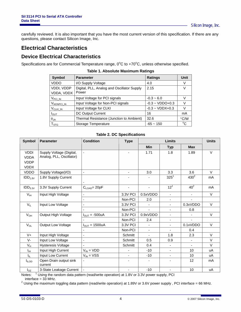
Electrical Characteristics Device Electrical Characteristics Specifications are for Commercial Temperature range, 0oC to +70oC, unless otherwise specified.
Table 1. Absolute Maximum Ratings Symbol Parameter Ratings Unit VDDO I/O Supply Voltage 4.0 V VDDI, VDDP VDDA, VDDX
Digital, PLL, Analog and Oscillator Supply Power
2.15 V
VPCI_IN Input Voltage for PCI signals -0.3 ~ 6.0 V VNONPCI_IN Input Voltage for Non-PCI signals -0.3 ~ VDDO+0.3 V VCLKI_IN Input Voltage for CLKI -0.3 ~ VDDX+0.3 V IOUT DC Output Current 16 mA θJA Thermal Resistance (Junction to Ambient) 32.6 °C/W TSTG Storage Temperature -65 ~ 150 oC
Table 2. DC Specifications
Limits Symbol Parameter Condition Type Min Typ Max
Units
VDDI VDDA VDDP VDDX
Supply Voltage (Digital, Analog, PLL, Oscillator)
- - 1.71 1.8 1.89 V
VDDO Supply Voltage(I/O) - - 3.0 3.3 3.6 V IDD1.8V 1.8V Supply Current
- - - 3251 4302 mA
IDD3.3V 3.3V Supply Current CLOAD= 20pF - - 121 402 mA
- 3.3V PCI 0.5xVDDO - - V VIH Input High Voltage - Non-PCI 2.0 - - - 3.3V PCI - - 0.3xVDDO V VIL Input Low Voltage - Non-PCI - - 0.8 IOUT = -500uA 3.3V PCI 0.9xVDDO - - V VOH Output High Voltage - Non-PCI 2.4 - - IOUT = 1500uA 3.3V PCI - - 0.1xVDDO V VOL Output Low Voltage - Non-PCI - - 0.4
V+ Input High Voltage - Schmitt - 1.8 2.3 V V- Input Low Voltage - Schmitt 0.5 0.9 - V VH Hysteresis Voltage - Schmitt 0.4 - - V IIH Input High Current VIN = VDD - -10 - 10 uA IIL Input Low Current VIN = VSS - -10 - 10 uA
IILOD Open Drain output sink current
- - - - 12 mA
IOZ 3-State Leakage Current - - -10 - 10 uA Notes: 1 Using the random data pattern (read/write operation) at 1.8V or 3.3V power supply, PCI
interface = 33 MHz. 2 Using the maximum toggling data pattern (read/write operation) at 1.89V or 3.6V power supply , PCI interface = 66 MHz.
SiI3114 PCI to Serial ATA Controller Data Sheet
Silicon Image, Inc.
© 2007 Silicon Image, Inc. 5 SiI-DS-0103-D
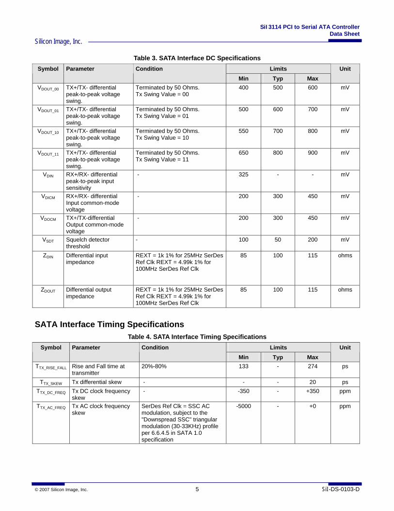
Table 3. SATA Interface DC Specifications Limits Symbol Parameter Condition
Min Typ Max Unit
VDOUT_00 TX+/TX- differential peak-to-peak voltage swing.
Terminated by 50 Ohms. Tx Swing Value = 00
400 500 600 mV
VDOUT_01 TX+/TX- differential peak-to-peak voltage swing.
Terminated by 50 Ohms. Tx Swing Value = 01
500 600 700 mV
VDOUT_10 TX+/TX- differential peak-to-peak voltage swing.
Terminated by 50 Ohms. Tx Swing Value = 10
550 700 800 mV
VDOUT_11 TX+/TX- differential peak-to-peak voltage swing.
Terminated by 50 Ohms. Tx Swing Value = 11
650 800 900 mV
VDIN RX+/RX- differential peak-to-peak input sensitivity
- 325 - - mV
VDICM RX+/RX- differential Input common-mode voltage
- 200 300 450 mV
VDOCM TX+/TX-differential Output common-mode voltage
- 200 300 450 mV
VSDT Squelch detector threshold
- 100 50 200 mV
ZDIN Differential input impedance
REXT = 1k 1% for 25MHz SerDes Ref Clk REXT = 4.99k 1% for 100MHz SerDes Ref Clk
85 100 115 ohms
ZDOUT Differential output impedance
REXT = 1k 1% for 25MHz SerDes Ref Clk REXT = 4.99k 1% for 100MHz SerDes Ref Clk
85 100 115 ohms
SATA Interface Timing Specifications Table 4. SATA Interface Timing Specifications
Limits Symbol Parameter Condition Min Typ Max
Unit
TTX_RISE_FALL Rise and Fall time at transmitter
20%-80% 133 - 274 ps
TTX_SKEW Tx differential skew - - - 20 ps TTX_DC_FREQ Tx DC clock frequency
skew - -350 - +350 ppm
TTX_AC_FREQ Tx AC clock frequency skew
SerDes Ref Clk = SSC AC modulation, subject to the "Downspread SSC" triangular modulation (30-33KHz) profile per 6.6.4.5 in SATA 1.0 specification
-5000 - +0 ppm
SiI3114 PCI to Serial ATA Controller Data Sheet
Silicon Image, Inc.
SiI-DS-0103-D 6 © 2007 Silicon Image, Inc.
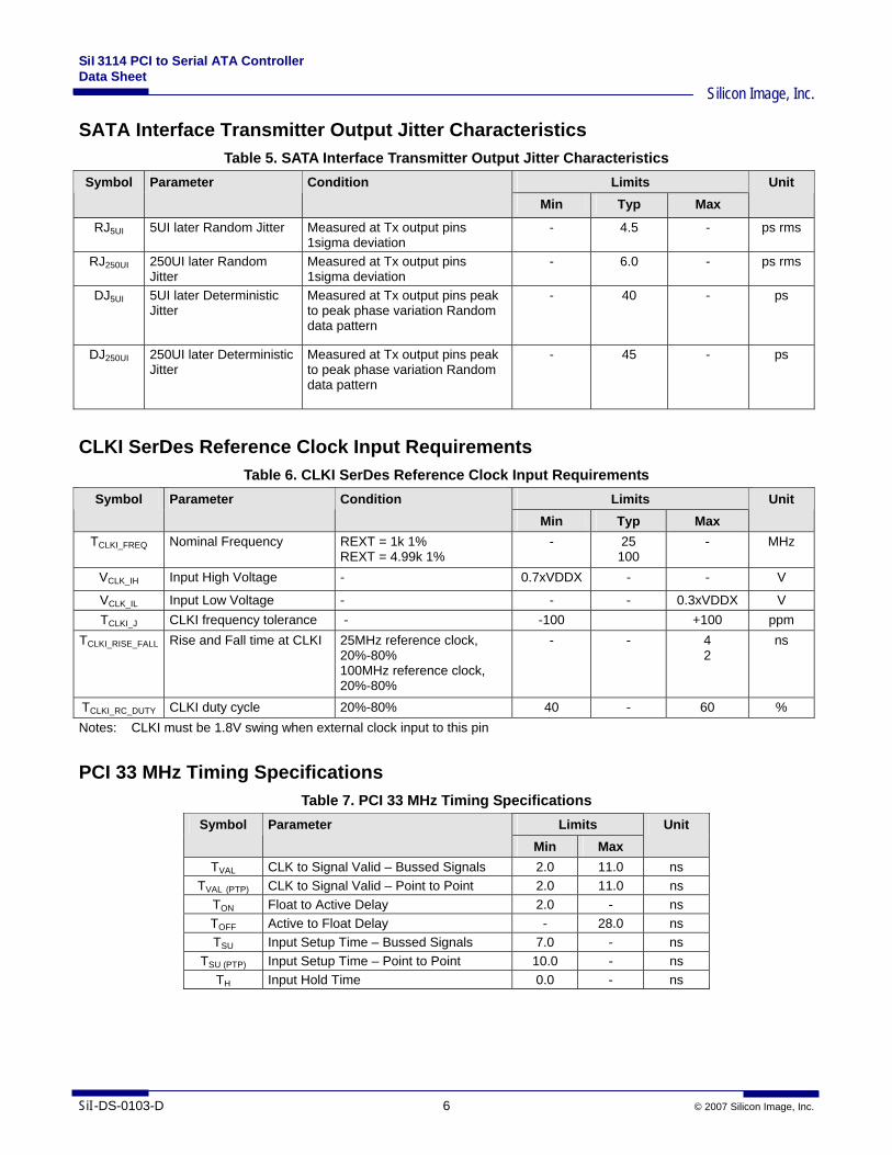
SATA Interface Transmitter Output Jitter Characteristics Table 5. SATA Interface Transmitter Output Jitter Characteristics
Limits Symbol Parameter Condition Min Typ Max
Unit
RJ5UI 5UI later Random Jitter Measured at Tx output pins 1sigma deviation
- 4.5 - ps rms
RJ250UI 250UI later Random Jitter
Measured at Tx output pins 1sigma deviation
- 6.0 - ps rms
DJ5UI 5UI later Deterministic Jitter
Measured at Tx output pins peak to peak phase variation Random data pattern
- 40 - ps
DJ250UI 250UI later Deterministic Jitter
Measured at Tx output pins peak to peak phase variation Random data pattern
- 45 - ps
CLKI SerDes Reference Clock Input Requirements Table 6. CLKI SerDes Reference Clock Input Requirements
Limits Symbol Parameter Condition Min Typ Max
Unit
TCLKI_FREQ Nominal Frequency REXT = 1k 1% REXT = 4.99k 1%
- 25 100
- MHz
VCLK_IH Input High Voltage - 0.7xVDDX - - V
VCLK_IL Input Low Voltage - - - 0.3xVDDX V TCLKI_J CLKI frequency tolerance - -100 +100 ppm
TCLKI_RISE_FALL Rise and Fall time at CLKI 25MHz reference clock, 20%-80% 100MHz reference clock, 20%-80%
- - 4 2
ns
TCLKI_RC_DUTY CLKI duty cycle 20%-80% 40 - 60 % Notes: CLKI must be 1.8V swing when external clock input to this pin
PCI 33 MHz Timing Specifications Table 7. PCI 33 MHz Timing Specifications
Limits Symbol Parameter Min Max
Unit
TVAL CLK to Signal Valid – Bussed Signals 2.0 11.0 ns TVAL (PTP) CLK to Signal Valid – Point to Point 2.0 11.0 ns
TON Float to Active Delay 2.0 - ns TOFF Active to Float Delay - 28.0 ns TSU Input Setup Time – Bussed Signals 7.0 - ns
TSU (PTP) Input Setup Time – Point to Point 10.0 - ns TH Input Hold Time 0.0 - ns
SiI3114 PCI to Serial ATA Controller Data Sheet
Silicon Image, Inc.
© 2007 Silicon Image, Inc. 7 SiI-DS-0103-D
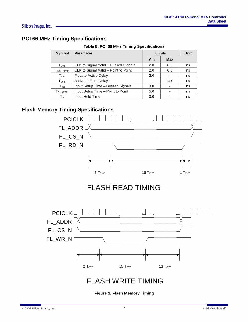
PCI 66 MHz Timing Specifications Table 8. PCI 66 MHz Timing Specifications
Limits Symbol Parameter Min Max
Unit
TVAL CLK to Signal Valid – Bussed Signals 2.0 6.0 ns TVAL (PTP) CLK to Signal Valid – Point to Point 2.0 6.0 ns
TON Float to Active Delay 2.0 - ns TOFF Active to Float Delay - 14.0 ns TSU Input Setup Time – Bussed Signals 3.0 - ns
TSU (PTP) Input Setup Time – Point to Point 5.0 - ns TH Input Hold Time 0.0 - ns
Flash Memory Timing Specifications PCICLK
FL_ADDR FL_CS_N FL_RD_N
2 TCYC 15 TCYC 1 TCYC
FLASH READ TIMING
PCICLKFL_ADDRFL_CS_NFL_WR_N
2 TCYC 15 TCYC 13 TCYC
FLASH WRITE TIMING
Figure 2. Flash Memory Timing
SiI3114 PCI to Serial ATA Controller Data Sheet
Silicon Image, Inc.
SiI-DS-0103-D 8 © 2007 Silicon Image, Inc.
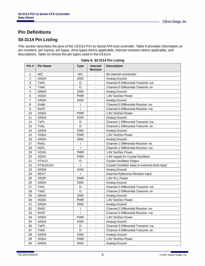
Pin Definitions SiI3114 Pin Listing This section describes the pins of the SiI3114 PCI-to-Serial ATA host controller. Table 9 provides information on pin numbers, pin names, pin types, drive types where applicable, internal resistors where applicable, and descriptions. Table 10 shows the pin types used in the SiI3114.
Table 9. SiI3114 Pin Listing Pin # Pin Name Type Internal
Resistor Description
1 N/C N/C - No internal connection 2 GNDA GND - Analog Ground 3 TxP0 O - Channel 0 Differential Transmit +ve 4 TxN0 O - Channel 0 Differential Transmit -ve 5 GNDA GND - Analog Ground 6 VDDA PWR - 1.8V SerDes Power 7 GNDA GND - Analog Ground 8 RxN0 I - Channel 0 Differential Receive -ve 9 RxP0 I - Channel 0 Differential Receive +ve
10 VDDA PWR - 1.8V SerDes Power 11 GNDA GND - Analog Ground 12 TxP1 O - Channel 1 Differential Transmit +ve 13 TxN1 O - Channel 1 Differential Transmit -ve 14 GNDA GND - Analog Ground 15 VDDA PWR - 1.8V SerDes Power 16 GNDA GND - Analog Ground 17 RxN1 I - Channel 1 Differential Receive -ve 18 RxP1 I - Channel 1 Differential Receive +ve 19 VDDA PWR - 1.8V SerDes Power 20 VDDX PWR - 1.8V supply for Crystal Oscillator 21 XTALO O - Crystal Oscillator Output 22 XTALI/CLKI I - Crystal Oscillator Input or external clock input 23 GNDA GND - Analog Ground 24 REXT I - External Reference Resistor Input 25 VDDP PWR - 1.8V PLL Power 26 GNDA GND - Analog Ground 27 TxP2 O - Channel 2 Differential Transmit +ve 28 TxN2 O - Channel 2 Differential Transmit -ve 29 GNDA GND - Analog Ground 30 VDDA PWR - 1.8V SerDes Power 31 GNDA GND - Analog Ground 32 RxN2 I - Channel 2 Differential Receive -ve 33 RxP2 I - Channel 2 Differential Receive +ve 34 VDDA PWR - 1.8V SerDes Power 35 GNDA GND - Analog Ground 36 TxP3 O - Channel 3 Differential Transmit +ve 37 TxN3 O - Channel 3 Differential Transmit -ve 38 GNDA GND - Analog Ground 39 VDDA PWR - 1.8V SerDes Power 40 GNDA GND - Analog Ground
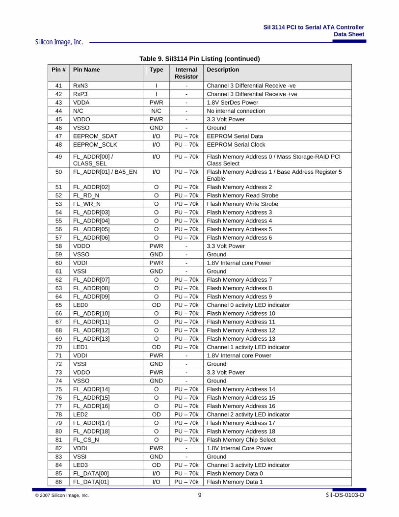
SiI3114 PCI to Serial ATA Controller Data Sheet
Silicon Image, Inc.
© 2007 Silicon Image, Inc. 9 SiI-DS-0103-D
Table 9. SiI3114 Pin Listing (continued) Pin # Pin Name Type Internal
Resistor Description
41 RxN3 I - Channel 3 Differential Receive -ve 42 RxP3 I - Channel 3 Differential Receive +ve 43 VDDA PWR - 1.8V SerDes Power 44 N/C N/C - No internal connection 45 VDDO PWR - 3.3 Volt Power 46 VSSO GND - Ground 47 EEPROM_SDAT I/O PU – 70k EEPROM Serial Data 48 EEPROM_SCLK I/O PU – 70k EEPROM Serial Clock
49 FL_ADDR[00] / CLASS_SEL
I/O PU – 70k Flash Memory Address 0 / Mass Storage-RAID PCI Class Select
50 FL_ADDR[01] / BA5_EN I/O PU – 70k Flash Memory Address 1 / Base Address Register 5 Enable
51 FL_ADDR[02] O PU – 70k Flash Memory Address 2 52 FL_RD_N O PU – 70k Flash Memory Read Strobe 53 FL_WR_N O PU – 70k Flash Memory Write Strobe 54 FL_ADDR[03] O PU – 70k Flash Memory Address 3 55 FL_ADDR[04] O PU – 70k Flash Memory Address 4 56 FL_ADDR[05] O PU – 70k Flash Memory Address 5 57 FL_ADDR[06] O PU – 70k Flash Memory Address 6 58 VDDO PWR - 3.3 Volt Power 59 VSSO GND - Ground 60 VDDI PWR - 1.8V Internal core Power 61 VSSI GND - Ground 62 FL_ADDR[07] O PU – 70k Flash Memory Address 7 63 FL_ADDR[08] O PU – 70k Flash Memory Address 8 64 FL_ADDR[09] O PU – 70k Flash Memory Address 9 65 LED0 OD PU – 70k Channel 0 activity LED indicator 66 FL_ADDR[10] O PU – 70k Flash Memory Address 10 67 FL_ADDR[11] O PU – 70k Flash Memory Address 11 68 FL_ADDR[12] O PU – 70k Flash Memory Address 12 69 FL_ADDR[13] O PU – 70k Flash Memory Address 13 70 LED1 OD PU – 70k Channel 1 activity LED indicator 71 VDDI PWR - 1.8V Internal core Power 72 VSSI GND - Ground 73 VDDO PWR - 3.3 Volt Power 74 VSSO GND - Ground 75 FL_ADDR[14] O PU – 70k Flash Memory Address 14 76 FL_ADDR[15] O PU – 70k Flash Memory Address 15 77 FL_ADDR[16] O PU – 70k Flash Memory Address 16 78 LED2 OD PU – 70k Channel 2 activity LED indicator 79 FL_ADDR[17] O PU – 70k Flash Memory Address 17 80 FL_ADDR[18] O PU – 70k Flash Memory Address 18 81 FL_CS_N O PU – 70k Flash Memory Chip Select 82 VDDI PWR - 1.8V Internal Core Power 83 VSSI GND - Ground 84 LED3 OD PU – 70k Channel 3 activity LED indicator 85 FL_DATA[00] I/O PU – 70k Flash Memory Data 0 86 FL_DATA[01] I/O PU – 70k Flash Memory Data 1
SiI3114 PCI to Serial ATA Controller Data Sheet
Silicon Image, Inc.
SiI-DS-0103-D 10 © 2007 Silicon Image, Inc.
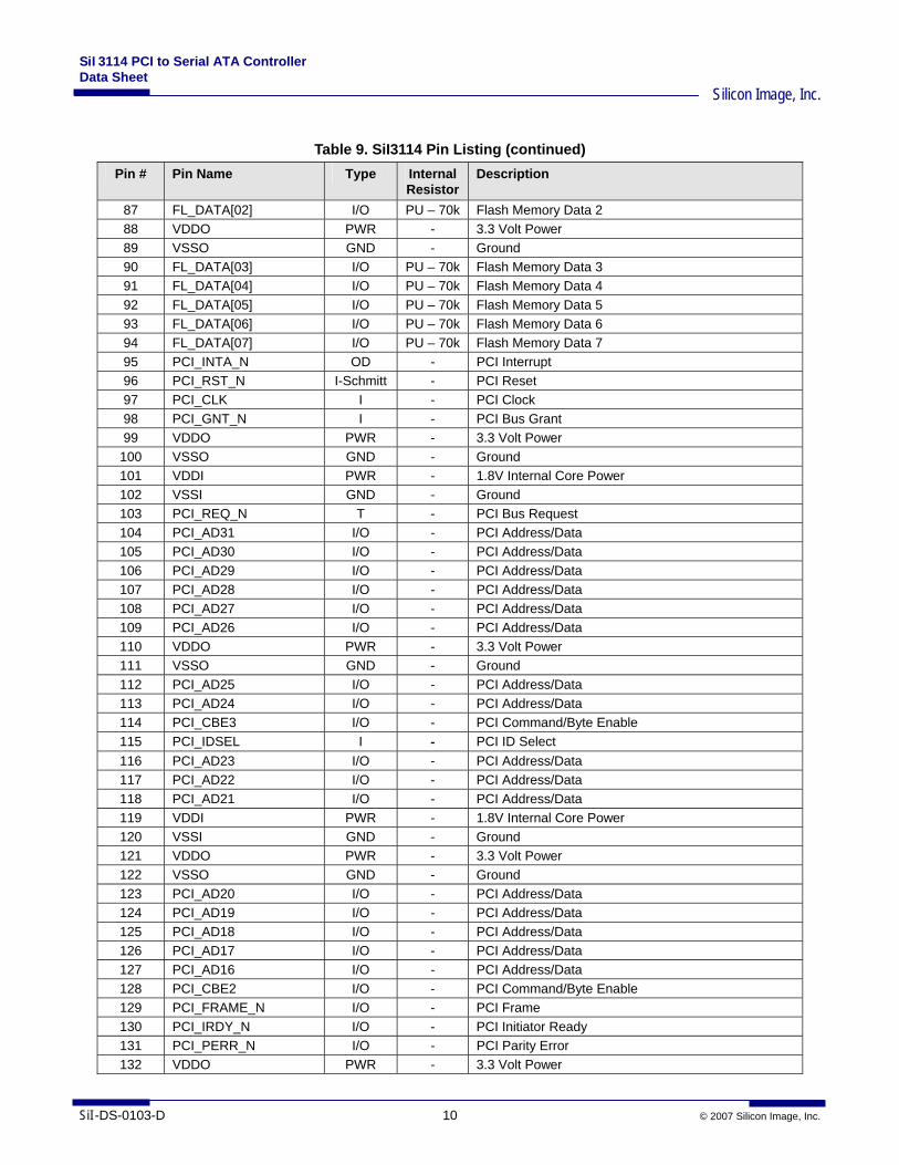
Table 9. SiI3114 Pin Listing (continued)
Pin # Pin Name Type Internal Resistor
Description
87 FL_DATA[02] I/O PU – 70k Flash Memory Data 2 88 VDDO PWR - 3.3 Volt Power 89 VSSO GND - Ground 90 FL_DATA[03] I/O PU – 70k Flash Memory Data 3 91 FL_DATA[04] I/O PU – 70k Flash Memory Data 4 92 FL_DATA[05] I/O PU – 70k Flash Memory Data 5 93 FL_DATA[06] I/O PU – 70k Flash Memory Data 6 94 FL_DATA[07] I/O PU – 70k Flash Memory Data 7 95 PCI_INTA_N OD - PCI Interrupt 96 PCI_RST_N I-Schmitt - PCI Reset 97 PCI_CLK I - PCI Clock 98 PCI_GNT_N I - PCI Bus Grant 99 VDDO PWR - 3.3 Volt Power
100 VSSO GND - Ground 101 VDDI PWR - 1.8V Internal Core Power 102 VSSI GND - Ground 103 PCI_REQ_N T - PCI Bus Request 104 PCI_AD31 I/O - PCI Address/Data 105 PCI_AD30 I/O - PCI Address/Data 106 PCI_AD29 I/O - PCI Address/Data 107 PCI_AD28 I/O - PCI Address/Data 108 PCI_AD27 I/O - PCI Address/Data 109 PCI_AD26 I/O - PCI Address/Data 110 VDDO PWR - 3.3 Volt Power 111 VSSO GND - Ground 112 PCI_AD25 I/O - PCI Address/Data 113 PCI_AD24 I/O - PCI Address/Data 114 PCI_CBE3 I/O - PCI Command/Byte Enable 115 PCI_IDSEL I - PCI ID Select 116 PCI_AD23 I/O - PCI Address/Data 117 PCI_AD22 I/O - PCI Address/Data 118 PCI_AD21 I/O - PCI Address/Data 119 VDDI PWR - 1.8V Internal Core Power 120 VSSI GND - Ground 121 VDDO PWR - 3.3 Volt Power 122 VSSO GND - Ground 123 PCI_AD20 I/O - PCI Address/Data 124 PCI_AD19 I/O - PCI Address/Data 125 PCI_AD18 I/O - PCI Address/Data 126 PCI_AD17 I/O - PCI Address/Data 127 PCI_AD16 I/O - PCI Address/Data 128 PCI_CBE2 I/O - PCI Command/Byte Enable 129 PCI_FRAME_N I/O - PCI Frame 130 PCI_IRDY_N I/O - PCI Initiator Ready 131 PCI_PERR_N I/O - PCI Parity Error 132 VDDO PWR - 3.3 Volt Power
SiI3114 PCI to Serial ATA Controller Data Sheet
Silicon Image, Inc.
© 2007 Silicon Image, Inc. 11 SiI-DS-0103-D
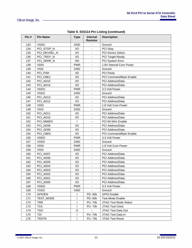
Table 9. SiI3114 Pin Listing (continued)
Pin # Pin Name Type Internal Resistor
Description
133 VSSO GND - Ground 134 PCI_STOP_N I/O - PCI Stop 135 PCI_DEVSEL_N I/O - PCI Device Select 136 PCI_TRDY_N I/O - PCI Target Ready 137 PCI_SERR_N OD - PCI System Error 138 VDDI PWR - 1.8V Internal Core Power 139 VSSI GND - Ground 140 PCI_PAR I/O - PCI Parity 141 PCI_CBE1 I/O - PCI Command/Byte Enable 142 PCI_AD15 I/O - PCI Address/Data 143 PCI_AD14 I/O - PCI Address/Data 144 VDDO PWR - 3.3 Volt Power 145 VSSO GND - Ground 146 PCI_AD13 I/O - PCI Address/Data 147 PCI_AD12 I/O - PCI Address/Data 148 VDDI PWR - 1.8 Volt Core Power 149 VSSI GND - Ground 150 PCI_AD11 I/O - PCI Address/Data 151 PCI_AD10 I/O - PCI Address/Data 152 PCI_M66EN I - PCI 66 MHz Enable 153 PCI_AD09 I/O - PCI Address/Data 154 PCI_AD08 I/O - PCI Address/Data 155 PCI_CBE0 I/O - PCI Command/Byte Enable 156 VDDO PWR - 3.3 Volt Power 157 VSSO GND - Ground 158 VDDI PWR - 1.8 Volt Core Power 159 VSSI GND - Ground 160 PCI_AD07 I/O - PCI Address/Data 161 PCI_AD06 I/O - PCI Address/Data 162 PCI_AD05 I/O - PCI Address/Data 163 PCI_AD04 I/O - PCI Address/Data 164 PCI_AD03 I/O - PCI Address/Data 165 PCI_AD02 I/O - PCI Address/Data 166 PCI_AD01 I/O - PCI Address/Data 167 PCI_AD00 I/O - PCI Address/Data 168 VDDO PWR - 3.3 Volt Power 169 VSSO GND - Ground 170 GPIOEN I PD -60k GPIO Enable 171 TEST_MODE I PD -60k Test Mode Enable 172 TMS I PU -70k JTAG Test Mode Select 173 TCK I PU -70k JTAG Test Clock 174 TDO O - JTAG Test Data Out 175 TDI I PU -70k JTAG Test Data In 176 TRSTN I PU -70k JTAG Test Reset
SiI3114 PCI to Serial ATA Controller Data Sheet
Silicon Image, Inc.
SiI-DS-0103-D 12 © 2007 Silicon Image, Inc.
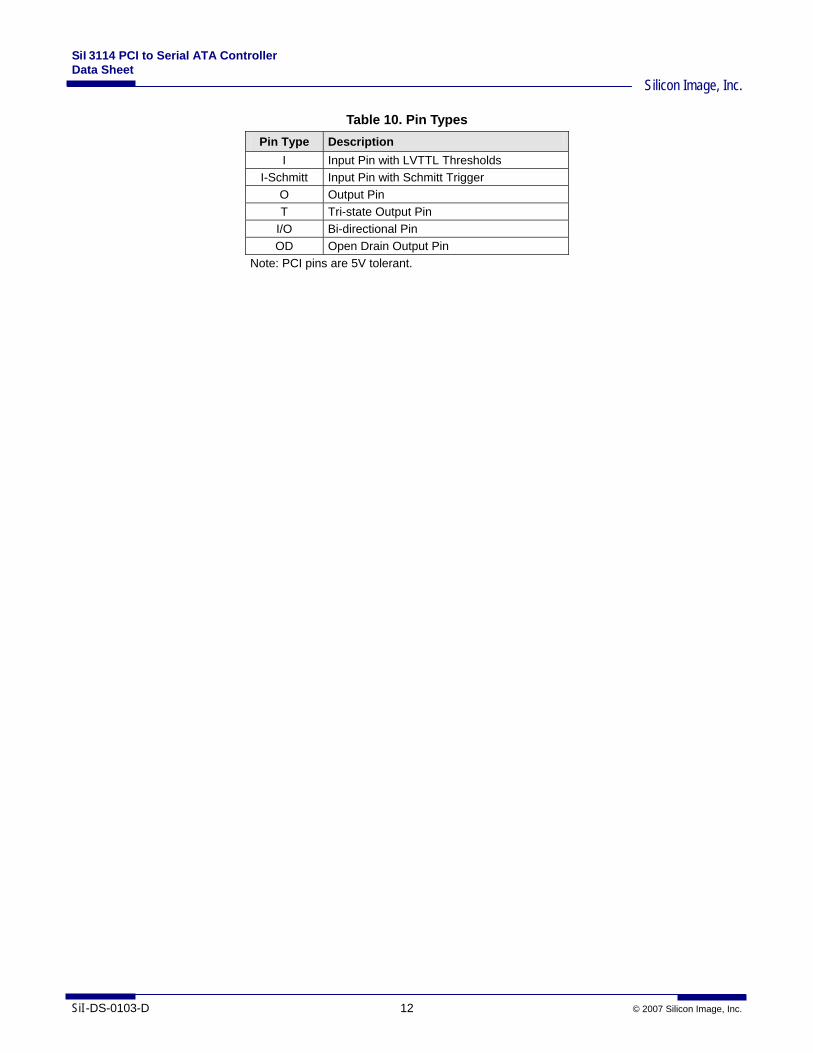
Table 10. Pin Types Pin Type Description
I Input Pin with LVTTL Thresholds I-Schmitt Input Pin with Schmitt Trigger
O Output Pin T Tri-state Output Pin
I/O Bi-directional Pin OD Open Drain Output Pin
Note: PCI pins are 5V tolerant.
SiI3114 PCI to Serial ATA Controller Data Sheet
Silicon Image, Inc.
© 2007 Silicon Image, Inc. 13 SiI-DS-0103-D
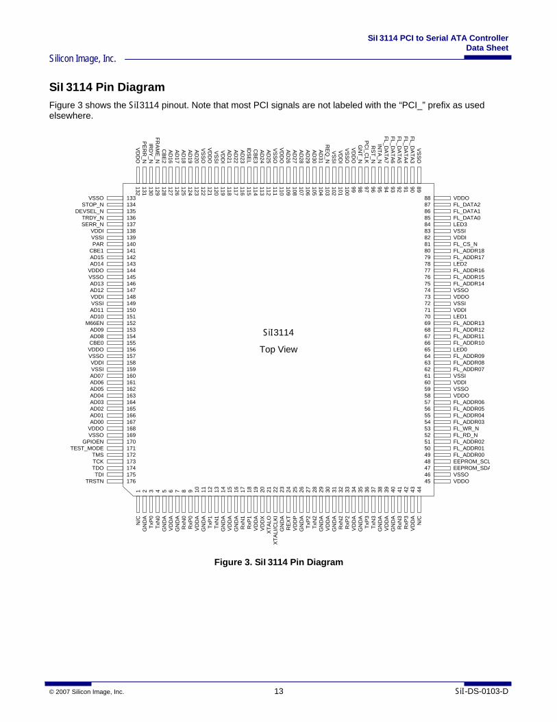
SiI3114 Pin Diagram Figure 3 shows the SiI3114 pinout. Note that most PCI signals are not labeled with the “PCI_” prefix as used elsewhere.
133 VSSO STOP_N
DEVSEL_N TRDY_N
134 135 136 137 138 139 140 141 142 143 144 145 146 147 148 149 150 151 152 153 154 155 156 157 158 159 160 161 162 163 164 165 166 167 168 169 170 171 172 173 174 175 176
SERR_N VDDI VSSI PAR
CBE1 AD15 AD14
VDDO VSSO AD13 AD12 VDDI VSSI AD11 AD10
M66EN AD09 AD08 CBE0 VDDO VSSO VDDI VSSI AD07 AD06 AD05 AD04 AD03 AD02 AD01 AD00
VDDO VSSO
GPIOEN TEST_MODE
TMS TCK TDO TDI
TRSTN
VDDO FL_DATA2FL_DATA1FL_DATA0LED3 VSSI VDDI FL_CS_N FL_ADDR18 FL_ADDR17 LED2 FL_ADDR16 FL_ADDR15 FL_ADDR14 VSSO VDDO VSSI VDDI LED1 FL_ADDR13 FL_ADDR12 FL_ADDR11 FL_ADDR10 LED0 FL_ADDR09 FL_ADDR08 FL_ADDR07 VSSI VDDI VSSO VDDO FL_ADDR06 FL_ADDR05 FL_ADDR04 FL_ADDR03 FL_WR_N FL_RD_N FL_ADDR02 FL_ADDR01 FL_ADDR00 EEPROM_SCLEEPROM_SDAVSSO VDDO
89 90 91 92 93 94 95 96 97 98 99 100 101 102 103 104 105 106 107 108 109 110 111 112 113 114 115 116 117 118 119 120 121 122 123 124 125 126 127 128 129 130 131 132
88 87 86 85 84 83 82 81 80 79 78 77 76 75 74 73 72 71 70 69 68 67 66 65 64 63 62 61 60 59 58 57 56 55 54 53 52 51 50 49 48 47 46 45
1 2 3 4 5 6 8 9 10
11
7 13
14
15
16
17
18
20
21
22
23
19
12
24
25
26
27
29
30
31
32
28
34
35
36
37
38
39
41
42
43
44
40
33
N/C
GN
DA
TxP
0Tx
N0
GN
DA
VD
DA
GN
DA
RxN
0R
xP0
VD
DA
GN
DA
TxP
1Tx
N1
GN
DA
VD
DA
GN
DA
RxN
1R
xP1
VD
DA
VD
DX
XTA
LOX
TALI
/CLK
IG
ND
AR
EX
TV
DD
PG
ND
ATx
P2
TxN
2G
ND
AV
DD
AG
ND
AR
xN2
RxP
2V
DD
AG
ND
ATx
P3
TxN
3G
ND
AV
DD
AG
ND
AR
xN3
RxP
3V
DD
AN
/CV
DD
OP
ER
R_N
IRD
Y_N
FRA
ME
_NC
BE
2A
D16
AD
17A
D18
AD
19A
D20
VS
SO
VD
DO
VS
SI
VD
DI
AD
21A
D22
AD
23ID
SE
LC
BE
3A
D24
AD
25V
SS
OV
DD
OA
D26
AD
27A
D28
AD
29A
D30
AD
31R
EQ
_NV
SS
IV
DD
IV
SS
OV
DD
OG
NT_N
PC
I_CLK
RS
T_NIN
TA_N
FL_DA
TA7
FL_DA
TA6
FL_DA
TA5
FL_DA
TA4
FL_DA
TA3
VS
SO
SiI3114
Top View
Figure 3. SiI3114 Pin Diagram
SiI3114 PCI to Serial ATA Controller Data Sheet
Silicon Image, Inc.
SiI-DS-0103-D 14 © 2007 Silicon Image, Inc.
SiI3114 Pin Descriptions PCI 66MHz 32-bit PCI Address and Data Pin Names: PCI_AD[31..00] Pin Numbers: 104-109, 112, 113, 116-118, 123-127, 142, 143, 146, 147, 150, 151, 153, 154, 160-167 Address and Data buses are multiplexed on the same PCI pins. A bus transaction consists of an address phase followed by one or more data phases. PCI supports both read and write bursts. The address phase is the first clock cycle in which PCI_FRAME_N signal is asserted. During the address phase, PCI_AD[31:0] contain a physical address (32 bits). For I/O, this can be a byte address. For configuration and memory it is a dword address. During data phases, PCI_AD[7:0] contain the least significant byte (LSB) and PCI_AD[31:24] contain the most significant byte (MSB). Write data is stable and valid when PCI_IRDY_N is asserted; read data is stable and valid when PCI_TRDY_N is asserted. Data is transferred during those clocks where both PCI_IRDY_N and PCI_TRDY_N are asserted. PCI Command and Byte Enables Pin Names: PCI_CBE[3..0] Pin Numbers: 114, 128, 141, 155 Command and Byte Enables are multiplexed on the same PCI pins. During the address phase of a transaction, PCI_CBE[3:0]_N define the bus command. During the data phase, PCI_CBE[3:0]_N are used as Byte Enables. Byte Enables are valid for the entire data phase and determine which byte lanes carry meaningful data. PCI ID Select Pin Name: PCI_IDSEL Pin Number: 115 This signal is used as a chip select during configuration read and write transactions. PCI Frame Cycle Pin Name: PCI_FRAME_N Pin Number: 129 Cycle Frame is driven by the current master to indicate the beginning and duration of an access. PCI_FRAME_N is asserted to indicate that a bus transaction is beginning. While PCI_FRAME_N is asserted, data transfers continue. When PCI_FRAME_N is deasserted, the transaction is in the final data phase or has completed. PCI Initiator Ready Pin Name: PCI_IRDY_N Pin Number: 130 Initiator Ready indicates the initializing agent’s (bus master’s) ability to complete the current data phase of the transaction. This signal is used with PCI_TRDY_N. A data phase is completed on any clock when both PCI_IRDY_N and PCI_TRDY_N are sampled as asserted. Wait cycles are inserted until both PCI_IRDY_N and PCI_TRDY_N are asserted together. PCI Target Ready Pin Name: PCI_TRDY_N Pin Number: 136 Target Ready indicates the target agent’s ability to complete the current data phase of the transaction. PCI_TRDY_N is used with PCI_IRDY_N. A data phase is completed on any clock when both PCI_TRDY_N and PCI_IRDY_N are sampled asserted. During a read, PCI_TRDY_N indicates that valid data is present on PCI_AD[31:0]. During a write, it indicates the target is prepared to accept data. PCI Device Select Pin Name: PCI_DEVSEL_N Pin Number: 135 Device Select, when actively driven, indicates the driving device has decoded its address as the target of the current access. As an input, PCI_DEVSEL_N indicates to a master whether any device on the bus has been selected.
SiI3114 PCI to Serial ATA Controller Data Sheet
Silicon Image, Inc.
© 2007 Silicon Image, Inc. 15 SiI-DS-0103-D
PCI Stop Pin Name: PCI_STOP_N Pin Number: 134 PCI_STOP_N indicates the current target is requesting that the master stop the current transaction. PCI Parity Error Pin Name: PCI_PERR_N Pin Number: 131 PCI_PERR_N indicates a data parity error between the current master and target on PCI. On a write transaction, the target always signals data parity errors back to the master on PCI_PERR_N. On a read transaction, the master asserts PCI_PERR_N to indicate to the system that an error was detected. PCI System Error Pin Name: PCI_SERR_N Pin Number: 137 System Error is for reporting address parity errors, data parity errors on Special Cycle Command, or any other system error where the result will be catastrophic. The PCI_SERR_N is a pure open drain and is actively driven for a single PCI clock by the agent reporting the error. The assertion of PCI_SERR_N is synchronous to the clock and meets the setup and hold times of all bused signals. However, the restoring of PCI_SERR_N to the deasserted state is accomplished by a weak pull-up. Note that if an agent does not want a non-maskable interrupt (NMI) to be generated, a different reporting mechanism is required. PCI Parity Pin Name: PCI_PAR Pin Number: 140 PCI_PAR is even parity across PCI_AD[31:0] and PCI_CBE[3:0]_N. Parity generation is required by all PCI agents. PCI_PAR is stable and valid one clock after the address phase. For data phases PCI_PAR is stable and valid one clock after either PCI_IRDY_N is asserted on a write transaction or PCI_TRDY_N is asserted on a read transaction. Once PCI_PAR is valid, it remains valid until one clock after the completion of the current data phase. (PCI_PAR has the same timing as PCI_AD[31:0] but delayed by one clock.) PCI Request Pin Name: PCI_REQ_N Pin Number: 103 This signal indicates to the arbiter that this agent desires use of the PCI bus. PCI Grant Pin Name: PCI_GNT_N Pin Number: 98 This signal indicates to the agent that access to the PCI bus has been granted. In response to a PCI request, this is a point-to-point signal. Every master has its own PCI_GNT_N, which must be ignored while PCI_RST_N is asserted. PCI Interrupt A Pin Name: PCI_INTA_N Pin Number: 95 Interrupt A is used to request an interrupt on the PCI bus. PCI_INTA_N is open collector and is an open drain output. PCI Clock Signal Pin Names: PCI_CLK Pin Number: 97 Clock Signal provides timing for all transactions on PCI and is an input to every PCI device. All other PCI signals (except PCI_RST_N, and PCI_INTA_N) are sampled on the rising edge of PCI_CLK. All other timing parameters are defined with respect to this edge.
SiI3114 PCI to Serial ATA Controller Data Sheet
Silicon Image, Inc.
SiI-DS-0103-D 16 © 2007 Silicon Image, Inc.
PCI Reset Pin Name: PCI_RST_N Pin Number: 96 PCI_RST_N is an active low input that is used to set the internal registers to their initial state. PCI_RST_N is typically the system power-on reset signal as distributed on the PCI bus. PCI M66EN Pin Name: PCI_M66EN Pin Number: 152 This pin configures the PCI bus operating frequency. When low, the PCI bus operates from 0 to 33 MHz. When high, the PCI bus operates from 33MHz to 66MHz.
Miscellaneous I/O Flash Signals Pin Name: FL_ADDR00 / CLASS_SEL Pin Number: 49 When PCI_RST_N is deasserted, this pin is an output and represents flash memory address bit 0. During reset, it is sampled to configure Mass Storage class or RAID mode in the PCI Class Code register. A high on this pin sets Mass Storage class, a low sets RAID mode. The configuration state is latched internally when PCI_RST_N is deasserted. This pad is internally pulled high to enable Mass Storage class if left unconnected. Pin Name: FL_ADDR01 / BA5_EN Pin Number: 50 When PCI_RST_N is deasserted, this pin is an output and represents flash memory address bit 1 During reset, it is sampled to configure Base address register 5. A high on this pin enables base address register 5, a low disables base address register 5. The configuration state is latched internally when PCI_RST_N is deasserted. This pin is internally pulled high to enable Base address register 5 when left unconnected. Pin Name: FL_ADDR[02-18] Pin Numbers: 51, 54-57, 62-64, 66-69, 75-77, 79, 80 Flash Memory address bits; 19 total for 512K address space. Flash address pins 14 to 18 are used to select internal test modes in conjunction with the TEST_MODE pin. Pin Name: FL_DATA[0-7] Pin Numbers: 85-87, 90-94 8-bit Flash memory data bus or GPIO pins Pin Name: FL_RD_N Pin Number: 52 Flash read enable signal, active low Pin Name: FL_WR_N Pin Number: 53 Flash write enable signal, active low Pin Name: FL_CS_N Pin Number: 81 Flash chip select signal, active low Serial EEPROM Interface Signals Pin Name: EEPROM_SDAT Pin Number: 47 Serial Interface (I2C) data line Pin Name: EEPROM_SCLK Pin Number: 48 Serial Interface (I2C) clock
SiI3114 PCI to Serial ATA Controller Data Sheet
Silicon Image, Inc.
© 2007 Silicon Image, Inc. 17 SiI-DS-0103-D
LED Drivers Pin Names: LED[0..3] Pin Numbers: 65, 70, 78, 84 These are 12mA open-drain outputs to drive Activity LEDs for Channels 0 to 3 respectively. GPIO Pin Name: GPIO_EN Pin Number: 170 This pin enables the use of the flash Data pins for General Purpose I/O. Test Pin Names: TMS, TCK, TDO, TDI, TRSTN Pin Numbers: 172-176 These pins are used for JTAG operation. The TRSTN pin must be tied to ground if the JTAG function is not used Pin Name: TEST_MODE Pin Number: 171 This pin is used for chip testing. This pin must be left open or tied to ground for normal operation. Power Supply & Ground Pin Name: VDDO Pin Numbers: 45, 58, 73, 88, 99, 110, 121, 132, 144, 156, 168 3.3 V Power Supply Input Pin Name: VDDI Pin Numbers: 60, 71, 82, 101, 119, 138, 148, 158 1.8V Power Supply Input for internal core Pin Name: VSSO Pin Number: 46, 59, 74, 89, 100, 111, 122, 133, 145, 157, 169 Ground reference point to power supply for I/O. Pin Name: VSSI Pin Number: 61, 72, 83, 102, 120, 139, 149, 159 Ground reference point to power supply for core.
Serial ATA Signals Power Supply & Ground Pin Name: VDDA Pin Numbers: 6, 10, 15, 19, 30, 34, 39, 43 SerDes 1.8 V Power supply Pins Pin Name: VDDP Pin Number: 25 PLL 1.8 V Power supply Pin Pin Name: VDDX Pin Number: 20 Oscillator 1.8 V Power supply Pin Pin Name: GNDA Pin Numbers: 2, 5, 7, 11, 14, 16, 23, 26, 29, 31, 35, 38, 40 SerDes Ground
SiI3114 PCI to Serial ATA Controller Data Sheet
Silicon Image, Inc.
SiI-DS-0103-D 18 © 2007 Silicon Image, Inc.
High Speed Serial Signals Pin Names: RxN[0..3] Pin Numbers: 8, 17, 32, 41 Differential receive negative side. Pin Names: RxP[0..3] Pin Numbers: 9, 18, 33, 42 Differential receive positive side. Pin Names: TxN[0..3] Pin Numbers: 4, 13, 28, 37 Differential transmit negative side Pin Names: TxP[0..3] Pin Numbers: 3, 12, 27, 36 Differential transmit positive side Other SerDes Signals Pin Name: XTALO Pin Number: 21 Crystal oscillator pin for SerDes reference clock. A 25MHz crystal must be used. Pin Name: XTALI/CLKI Pin Number: 22 Crystal oscillator pin for SerDes reference clock. When external clock source is selected, the external clock (either 25MHz or 100 MHz) will come in through this pin. The clock must be 1.8V swing and the precision requirement is ±100ppm. Pin Name: REXT Pin Number: 24 External reference resistor pin for termination calibration. This pin provides the additional function of selecting frequency of the clock source. For 25MHz, a 1K, 1% resistor is connected to ground. For 100MHz, a 4.99K, 1% resistor is connected to ground.

SiI3114 PCI to Serial ATA Controller Data Sheet
Silicon Image, Inc.
© 2007 Silicon Image, Inc. 19 SiI-DS-0103-D
Package Drawing
Figure 4. Package Drawing – 176 TQFP Part Ordering Number: SiI3114CT176 (176 pin TQFP standard package) SiI3114CTU (176 pin TQFP universal package)
PIN #1
44
88
89
132
133176
20.0 SQ NOM
22.0 SQ NOM
0.40 NOM 0.18 NOM45
0.10 NOM
1.00 NOM
Dimensions in millimeters
SiI3114 PCI to Serial ATA Controller Data Sheet
Silicon Image, Inc.
SiI-DS-0103-D 20 © 2007 Silicon Image, Inc.
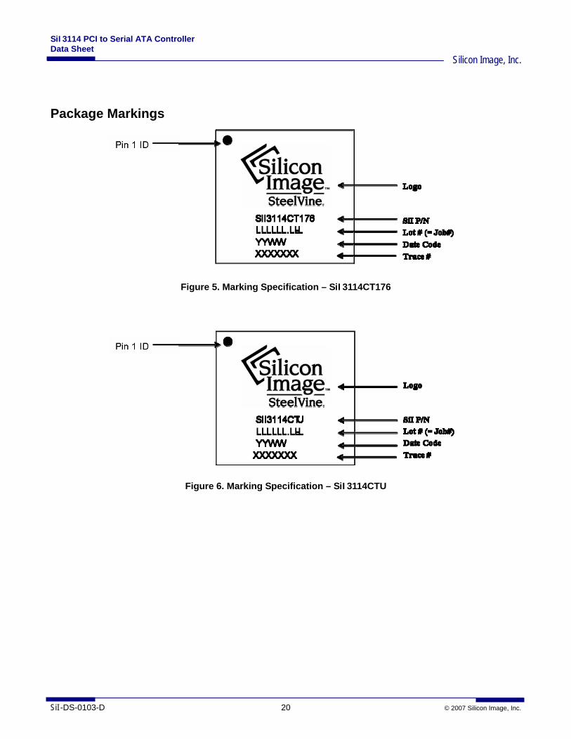
Package Markings
Figure 5. Marking Specification – SiI3114CT176
Figure 6. Marking Specification – SiI3114CTU
SiI3114 PCI to Serial ATA Controller Data Sheet
Silicon Image, Inc.
© 2007 Silicon Image, Inc. 21 SiI-DS-0103-D
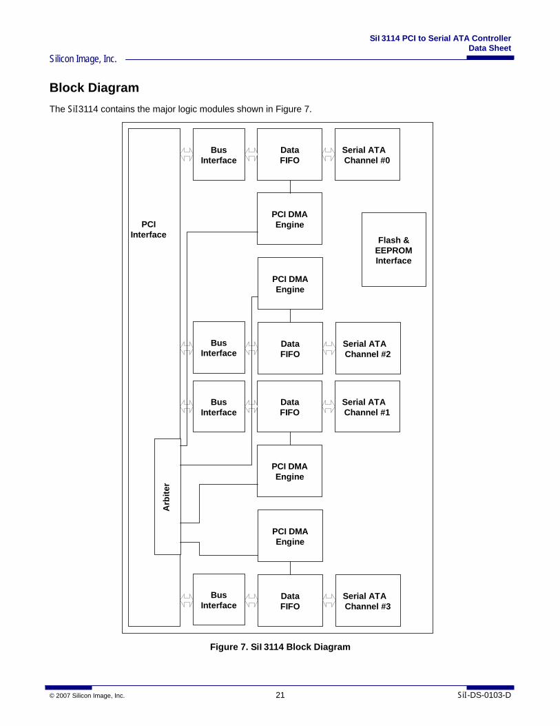
Block Diagram The SiI3114 contains the major logic modules shown in Figure 7.
PCI Interface
Arb
iter
Flash & EEPROM Interface
Serial ATA Channel #0
PCI DMA Engine
Data FIFO
Bus Interface
Serial ATA Channel #2
Data FIFO
PCI DMA Engine
Bus Interface
Serial ATA Channel #1
PCI DMA Engine
Data FIFO
Bus Interface
Serial ATA Channel #3
Data FIFO
PCI DMA Engine
Bus Interface
Figure 7. SiI3114 Block Diagram
SiI3114 PCI to Serial ATA Controller Data Sheet
Silicon Image, Inc.
SiI-DS-0103-D 22 © 2007 Silicon Image, Inc.
Auto-Initialization The SiI3114 supports an external flash and/or EEPROM device for BIOS extensions and user-defined PCI configuration header data.
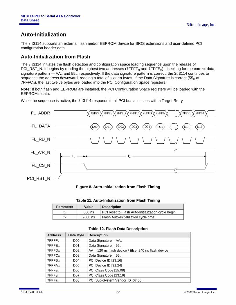
Auto-Initialization from Flash The SiI3114 initiates the flash detection and configuration space loading sequence upon the release of PCI_RST_N. It begins by reading the highest two addresses (7FFFFH and 7FFFEH), checking for the correct data signature pattern — AAH and 55H, respectively. If the data signature pattern is correct, the SiI3114 continues to sequence the address downward, reading a total of sixteen bytes. If the Data Signature is correct (55H at 7FFFCH), the last twelve bytes are loaded into the PCI Configuration Space registers.
Note: If both flash and EEPROM are installed, the PCI Configuration Space registers will be loaded with the EEPROM’s data.
While the sequence is active, the SiI3114 responds to all PCI bus accesses with a Target Retry.
D15D14 D05D04D03D02D01D00
FL_ADDR
MEM_ADDR FL_DATA
FL_RD_N
FL_WR_N
FL_CS_N
PCI_RST_N
t1 t2
7FFFF 7FFFE 7FFFD 7FFFC 7FFFB 7FFFA 7FFF1 7FFF0
Figure 8. Auto-Initialization from Flash Timing
Table 11. Auto-Initialization from Flash Timing Parameter Value Description
t1 660 ns PCI reset to Flash Auto-Initialization cycle begin t2 9600 ns Flash Auto-Initialization cycle time
Table 12. Flash Data Description
Address Data Byte Description 7FFFFH D00 Data Signature = AAH 7FFFEH D01 Data Signature = 55H 7FFFDH D02 AA = 120 ns flash device / Else, 240 ns flash device 7FFFCH D03 Data Signature = 55H 7FFFBH D04 PCI Device ID [23:16] 7FFFAH D05 PCI Device ID [31:24] 7FFF9H D06 PCI Class Code [15:08] 7FFF8H D07 PCI Class Code [23:16] 7FFF7H D08 PCI Sub-System Vendor ID [07:00]
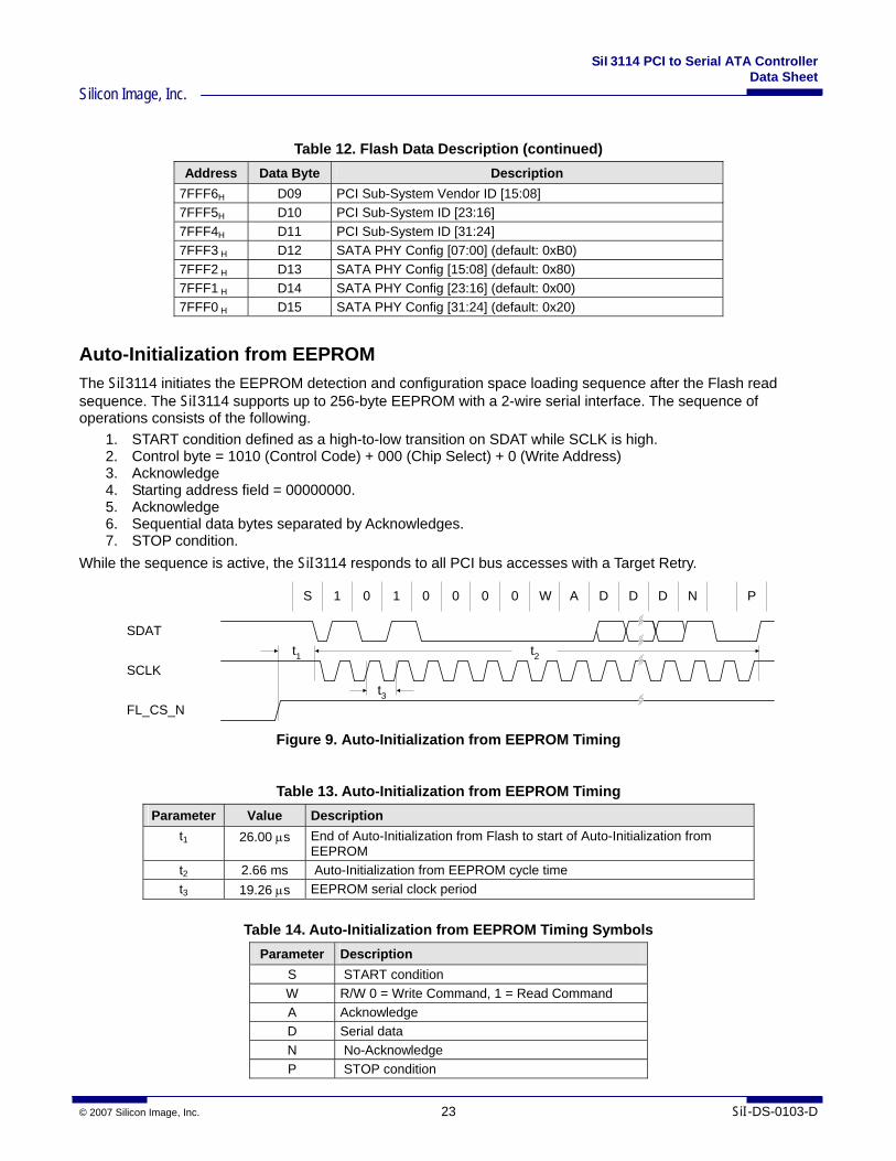
SiI3114 PCI to Serial ATA Controller Data Sheet
Silicon Image, Inc.
© 2007 Silicon Image, Inc. 23 SiI-DS-0103-D
Table 12. Flash Data Description (continued)
Address Data Byte Description 7FFF6H D09 PCI Sub-System Vendor ID [15:08] 7FFF5H D10 PCI Sub-System ID [23:16] 7FFF4H D11 PCI Sub-System ID [31:24] 7FFF3 H D12 SATA PHY Config [07:00] (default: 0xB0) 7FFF2 H D13 SATA PHY Config [15:08] (default: 0x80) 7FFF1 H D14 SATA PHY Config [23:16] (default: 0x00) 7FFF0 H D15 SATA PHY Config [31:24] (default: 0x20)
Auto-Initialization from EEPROM The SiI3114 initiates the EEPROM detection and configuration space loading sequence after the Flash read sequence. The SiI3114 supports up to 256-byte EEPROM with a 2-wire serial interface. The sequence of operations consists of the following.
1. START condition defined as a high-to-low transition on SDAT while SCLK is high. 2. Control byte = 1010 (Control Code) + 000 (Chip Select) + 0 (Write Address) 3. Acknowledge 4. Starting address field = 00000000. 5. Acknowledge 6. Sequential data bytes separated by Acknowledges. 7. STOP condition.
While the sequence is active, the SiI3114 responds to all PCI bus accesses with a Target Retry.
FL_CS_N
SCLK
SDATt1 t2
S 1 0 1 0 0 0 0 W PA ND D D
t3
Figure 9. Auto-Initialization from EEPROM Timing
Table 13. Auto-Initialization from EEPROM Timing Parameter Value Description
t1 26.00 μs End of Auto-Initialization from Flash to start of Auto-Initialization from EEPROM
t2 2.66 ms Auto-Initialization from EEPROM cycle time t3 19.26 μs EEPROM serial clock period
Table 14. Auto-Initialization from EEPROM Timing Symbols
Parameter Description S START condition W R/W 0 = Write Command, 1 = Read Command A Acknowledge D Serial data N No-Acknowledge P STOP condition
SiI3114 PCI to Serial ATA Controller Data Sheet
Silicon Image, Inc.
SiI-DS-0103-D 24 © 2007 Silicon Image, Inc.
Table 15. EEPROM Data Description
Address Data Byte Description 00H D00 Memory Present Pattern = AAH 01H D01 Memory Present Pattern = 55H 02H D02 Data Signature = AAH 03H D03 Data Signature = 55H 04H D04 PCI Device ID [23:16] 05H D05 PCI Device ID [31:24] 06H D06 PCI Class Code [15:08] 07H D07 PCI Class Code [23:16] 08H D08 PCI Sub-System Vendor ID [07:00] 09H D09 PCI Sub-System Vendor ID [15:08] 0AH D10 PCI Sub-System ID [23:16] 0BH D11 PCI Sub-System ID [31:24] 0CH D12 SATA PHY Config [07:00] (default: 0xB0) 0DH D13 SATA PHY Config [15:08] (default: 0x80) 0EH D14 SATA PHY Config [23:16] (default: 0x00) 0FH D15 SATA PHY Config [31:24] (default: 0x20)
SiI3114 PCI to Serial ATA Controller Data Sheet
Silicon Image, Inc.
© 2007 Silicon Image, Inc. 25 SiI-DS-0103-D
Register Definitions This section describes the registers within the SiI3114.
PCI Configuration Space The PCI Configuration Space registers define he operation of the SiI3114 on the PCI bus. These registers are accessible only when the SiI3114 detects a Configuration Read or Write operation, with its IDSEL asserted, on the 32-bit PCI bus. Table 16 outlines the PCI Configuration space for the SiI3114.
Table 16. SiI3114 PCI Configuration Space Register Name Address
Offset 31 16 15 00 Access
Type
00H Device ID Vendor ID R/W 04H PCI Status PCI Command R/W 08H PCI Class Code Revision ID R/W 0CH BIST Header Type Latency Timer Cache Line Size R/W 10H Base Address Register 0 R/W 14H Base Address Register 1 R/W 18H Base Address Register 2 R/W 1CH Base Address Register 3 R/W 20H Base Address Register 4 R/W 24H Base Address Register 5 R/W 28H Reserved - 2CH Subsystem ID Subsystem Vendor ID R/W 30H Expansion ROM Base Address R/W 34H Reserved Capabilities Ptr R 38H Reserved R/W 3CH Max Latency Min Grant Interrupt Pin Interrupt Line R/W 40H Reserved Configuration R/W 44H Software Data Register R/W 48H Reserved - 4CH Reserved - 50H Reserved - 54H Reserved - 58H Reserved - 5CH Reserved - 60H Power Management Capabilities Next Item Pointer Capability ID R/W 64H Data Reserved Functions Control and Status R/W 68H Reserved - 6CH Reserved - 70H Reserved PCI Bus Master
Status – Channel 0/2
Reserved PCI Bus Master Command – Channel 0/2
R/W
74H PRD Table Address – Channel 0/2 R/W 78H Reserved PCI Bus Master
Status – Channel 1/3
Reserved PCI Bus Master Command – Channel 1/3
R/W
7CH PRD Table Address – Channel 1/3 R/W 80H Reserved Channel 0/2 Data
Transfer Mode R/W
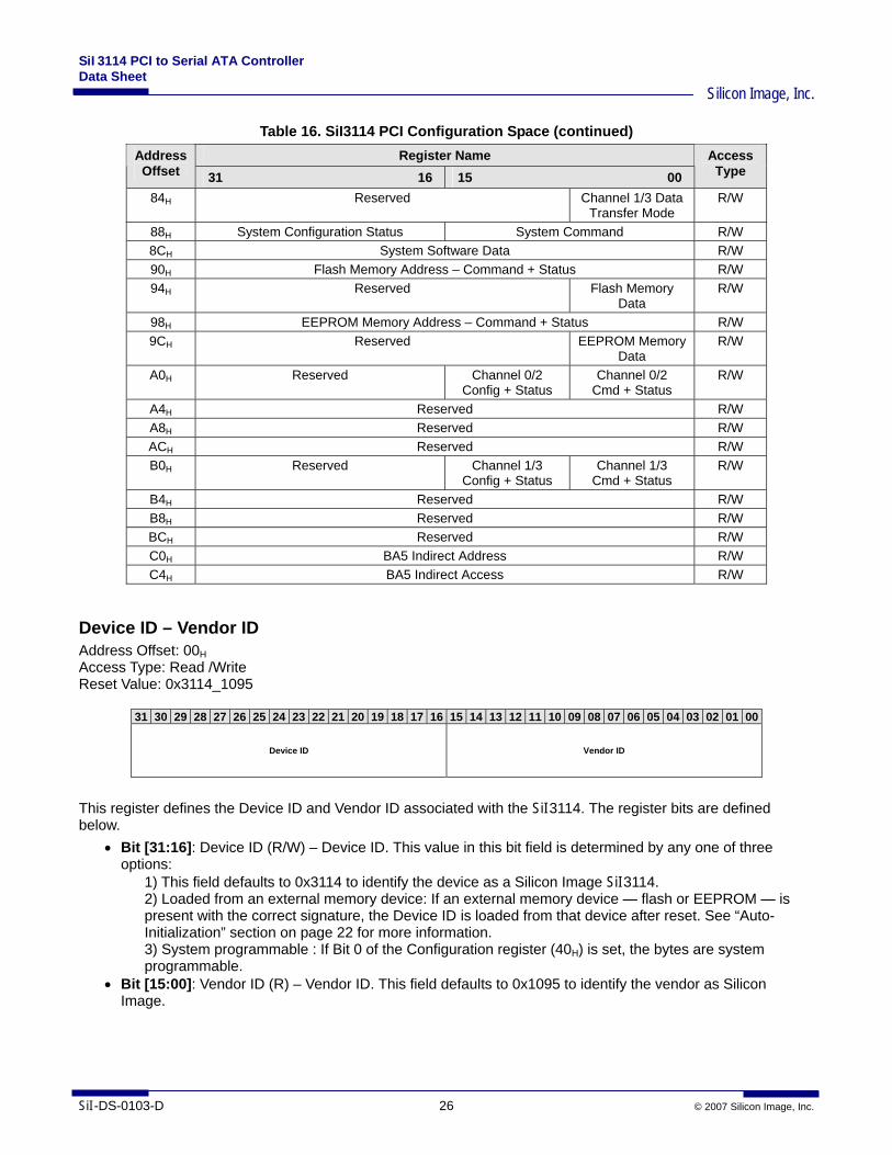
SiI3114 PCI to Serial ATA Controller Data Sheet
Silicon Image, Inc.
SiI-DS-0103-D 26 © 2007 Silicon Image, Inc.
Table 16. SiI3114 PCI Configuration Space (continued) Register Name Address
Offset 31 16 15 00 Access
Type
84H Reserved Channel 1/3 Data Transfer Mode
R/W
88H System Configuration Status System Command R/W 8CH System Software Data R/W 90H Flash Memory Address – Command + Status R/W 94H Reserved Flash Memory
Data R/W
98H EEPROM Memory Address – Command + Status R/W 9CH Reserved EEPROM Memory
Data R/W
A0H Reserved Channel 0/2 Config + Status
Channel 0/2 Cmd + Status
R/W
A4H Reserved R/W A8H Reserved R/W ACH Reserved R/W B0H Reserved Channel 1/3
Config + Status Channel 1/3
Cmd + Status R/W
B4H Reserved R/W B8H Reserved R/W BCH Reserved R/W C0H BA5 Indirect Address R/W C4H BA5 Indirect Access R/W
Device ID – Vendor ID Address Offset: 00H Access Type: Read /Write Reset Value: 0x3114_1095
31 30 29 28 27 26 25 24 23 22 21 20 19 18 17 16 15 14 13 12 11 10 09 08 07 06 05 04 03 02 01 00
Device ID Vendor ID
This register defines the Device ID and Vendor ID associated with the SiI3114. The register bits are defined below.
• Bit [31:16]: Device ID (R/W) – Device ID. This value in this bit field is determined by any one of three options:
1) This field defaults to 0x3114 to identify the device as a Silicon Image SiI3114. 2) Loaded from an external memory device: If an external memory device — flash or EEPROM — is present with the correct signature, the Device ID is loaded from that device after reset. See “Auto-Initialization” section on page 22 for more information. 3) System programmable : If Bit 0 of the Configuration register (40H) is set, the bytes are system programmable.
• Bit [15:00]: Vendor ID (R) – Vendor ID. This field defaults to 0x1095 to identify the vendor as Silicon Image.
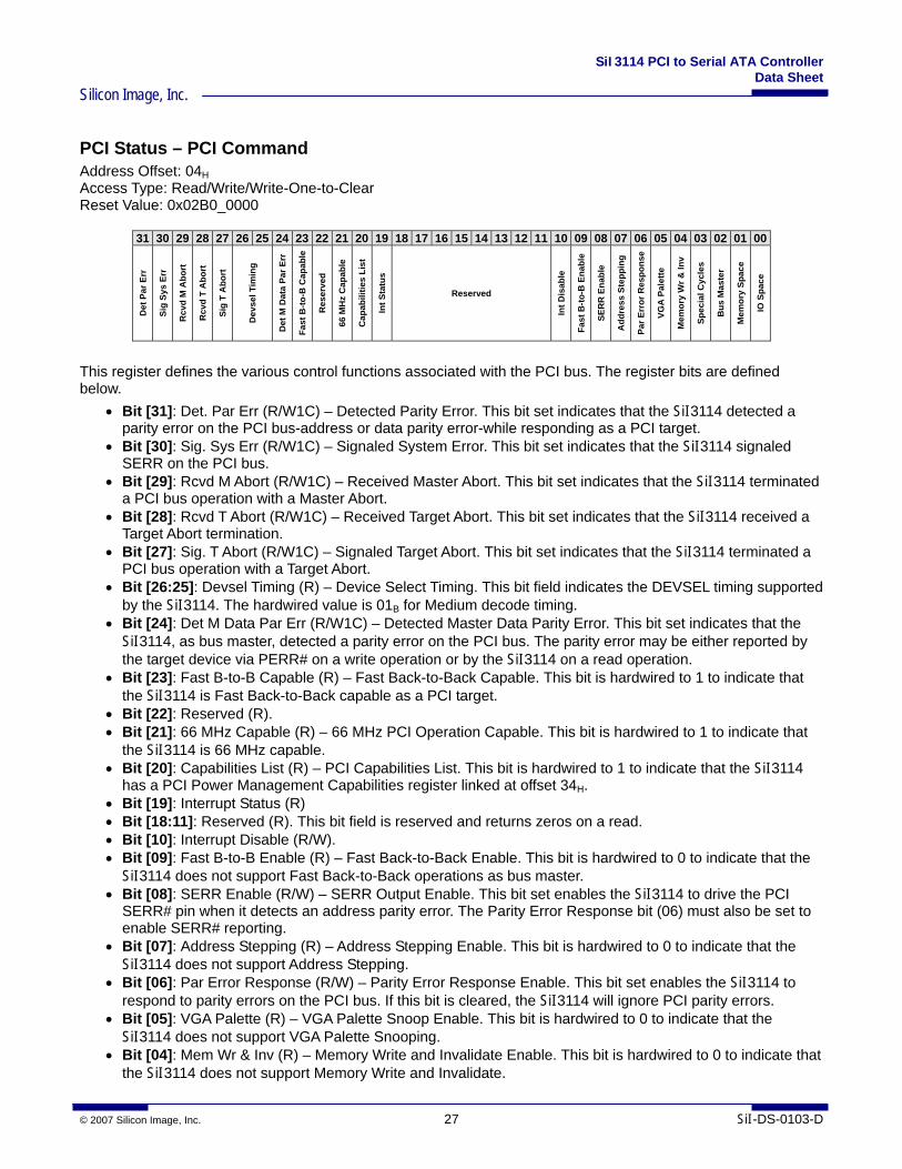
SiI3114 PCI to Serial ATA Controller Data Sheet
Silicon Image, Inc.
© 2007 Silicon Image, Inc. 27 SiI-DS-0103-D
PCI Status – PCI Command Address Offset: 04H Access Type: Read/Write/Write-One-to-Clear Reset Value: 0x02B0_0000
31 30 29 28 27 26 25 24 23 22 21 20 19 18 17 16 15 14 13 12 11 10 09 08 07 06 05 04 03 02 01 00
Det
Par
Err
Sig
Sys
Err
Rcv
d M
Abo
rt
Rcv
d T
Abo
rt
Sig
T A
bort
Dev
sel T
imin
g
Det
M D
ata
Par E
rr
Fast
B-to
-B C
apab
le
Res
erve
d
66 M
Hz
Cap
able
Cap
abili
ties
List
Int S
tatu
s
Reserved
Int D
isab
le
Fast
B-to
-B E
nabl
e
SER
R E
nabl
e
Add
ress
Ste
ppin
g
Par E
rror
Res
pons
e
VGA
Pal
ette
Mem
ory
Wr &
Inv
Spec
ial C
ycle
s
Bus
Mas
ter
Mem
ory
Spac
e
IO S
pace
This register defines the various control functions associated with the PCI bus. The register bits are defined below.
• Bit [31]: Det. Par Err (R/W1C) – Detected Parity Error. This bit set indicates that the SiI3114 detected a parity error on the PCI bus-address or data parity error-while responding as a PCI target.
• Bit [30]: Sig. Sys Err (R/W1C) – Signaled System Error. This bit set indicates that the SiI3114 signaled SERR on the PCI bus.
• Bit [29]: Rcvd M Abort (R/W1C) – Received Master Abort. This bit set indicates that the SiI3114 terminated a PCI bus operation with a Master Abort.
• Bit [28]: Rcvd T Abort (R/W1C) – Received Target Abort. This bit set indicates that the SiI3114 received a Target Abort termination.
• Bit [27]: Sig. T Abort (R/W1C) – Signaled Target Abort. This bit set indicates that the SiI3114 terminated a PCI bus operation with a Target Abort.
• Bit [26:25]: Devsel Timing (R) – Device Select Timing. This bit field indicates the DEVSEL timing supported by the SiI3114. The hardwired value is 01B for Medium decode timing.
• Bit [24]: Det M Data Par Err (R/W1C) – Detected Master Data Parity Error. This bit set indicates that the SiI3114, as bus master, detected a parity error on the PCI bus. The parity error may be either reported by the target device via PERR# on a write operation or by the SiI3114 on a read operation.
• Bit [23]: Fast B-to-B Capable (R) – Fast Back-to-Back Capable. This bit is hardwired to 1 to indicate that the SiI3114 is Fast Back-to-Back capable as a PCI target.
• Bit [22]: Reserved (R). • Bit [21]: 66 MHz Capable (R) – 66 MHz PCI Operation Capable. This bit is hardwired to 1 to indicate that
the SiI3114 is 66 MHz capable. • Bit [20]: Capabilities List (R) – PCI Capabilities List. This bit is hardwired to 1 to indicate that the SiI3114
has a PCI Power Management Capabilities register linked at offset 34H. • Bit [19]: Interrupt Status (R) • Bit [18:11]: Reserved (R). This bit field is reserved and returns zeros on a read. • Bit [10]: Interrupt Disable (R/W). • Bit [09]: Fast B-to-B Enable (R) – Fast Back-to-Back Enable. This bit is hardwired to 0 to indicate that the
SiI3114 does not support Fast Back-to-Back operations as bus master. • Bit [08]: SERR Enable (R/W) – SERR Output Enable. This bit set enables the SiI3114 to drive the PCI
SERR# pin when it detects an address parity error. The Parity Error Response bit (06) must also be set to enable SERR# reporting.
• Bit [07]: Address Stepping (R) – Address Stepping Enable. This bit is hardwired to 0 to indicate that the SiI3114 does not support Address Stepping.
• Bit [06]: Par Error Response (R/W) – Parity Error Response Enable. This bit set enables the SiI3114 to respond to parity errors on the PCI bus. If this bit is cleared, the SiI3114 will ignore PCI parity errors.
• Bit [05]: VGA Palette (R) – VGA Palette Snoop Enable. This bit is hardwired to 0 to indicate that the SiI3114 does not support VGA Palette Snooping.
• Bit [04]: Mem Wr & Inv (R) – Memory Write and Invalidate Enable. This bit is hardwired to 0 to indicate that the SiI3114 does not support Memory Write and Invalidate.
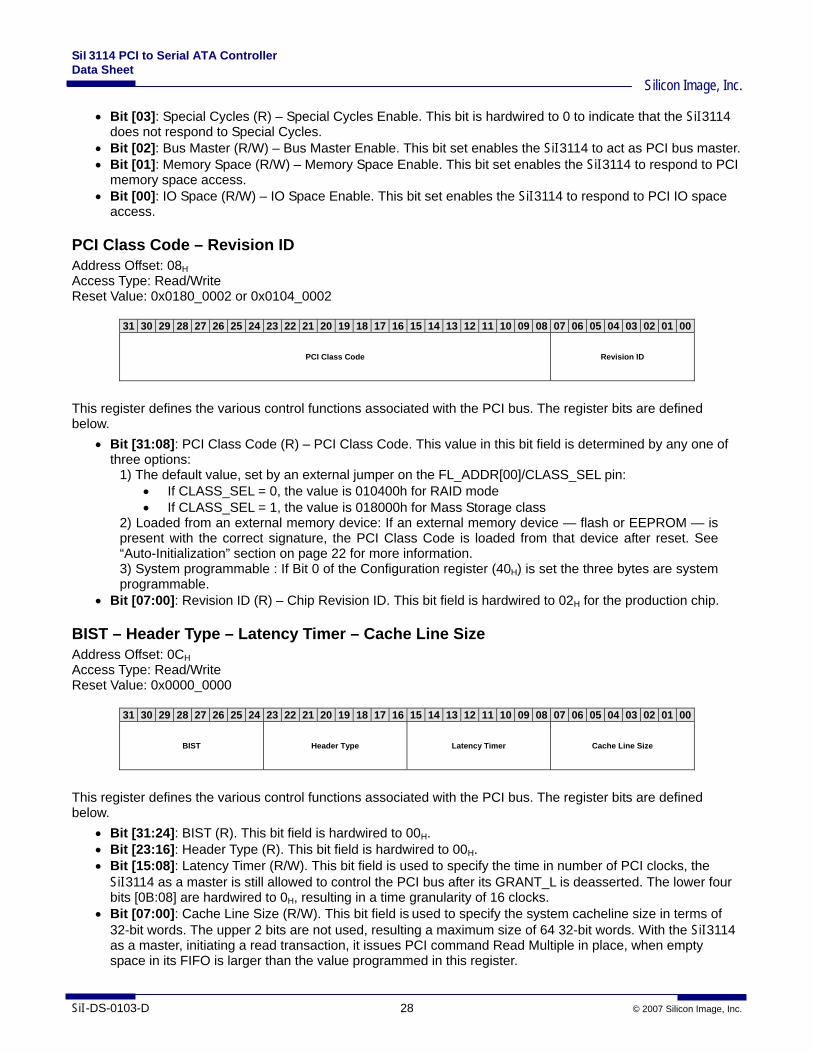
SiI3114 PCI to Serial ATA Controller Data Sheet
Silicon Image, Inc.
SiI-DS-0103-D 28 © 2007 Silicon Image, Inc.
• Bit [03]: Special Cycles (R) – Special Cycles Enable. This bit is hardwired to 0 to indicate that the SiI3114 does not respond to Special Cycles.
• Bit [02]: Bus Master (R/W) – Bus Master Enable. This bit set enables the SiI3114 to act as PCI bus master. • Bit [01]: Memory Space (R/W) – Memory Space Enable. This bit set enables the SiI3114 to respond to PCI
memory space access. • Bit [00]: IO Space (R/W) – IO Space Enable. This bit set enables the SiI3114 to respond to PCI IO space
access.
PCI Class Code – Revision ID Address Offset: 08H Access Type: Read/Write Reset Value: 0x0180_0002 or 0x0104_0002
31 30 29 28 27 26 25 24 23 22 21 20 19 18 17 16 15 14 13 12 11 10 09 08 07 06 05 04 03 02 01 00
PCI Class Code Revision ID
This register defines the various control functions associated with the PCI bus. The register bits are defined below.
• Bit [31:08]: PCI Class Code (R) – PCI Class Code. This value in this bit field is determined by any one of three options:
1) The default value, set by an external jumper on the FL_ADDR[00]/CLASS_SEL pin: • If CLASS_SEL = 0, the value is 010400h for RAID mode • If CLASS_SEL = 1, the value is 018000h for Mass Storage class
2) Loaded from an external memory device: If an external memory device — flash or EEPROM — is present with the correct signature, the PCI Class Code is loaded from that device after reset. See “Auto-Initialization” section on page 22 for more information. 3) System programmable : If Bit 0 of the Configuration register (40H) is set the three bytes are system programmable.
• Bit [07:00]: Revision ID (R) – Chip Revision ID. This bit field is hardwired to 02H for the production chip.
BIST – Header Type – Latency Timer – Cache Line Size Address Offset: 0CH Access Type: Read/Write Reset Value: 0x0000_0000
31 30 29 28 27 26 25 24 23 22 21 20 19 18 17 16 15 14 13 12 11 10 09 08 07 06 05 04 03 02 01 00
BIST Header Type Latency Timer Cache Line Size
This register defines the various control functions associated with the PCI bus. The register bits are defined below.
• Bit [31:24]: BIST (R). This bit field is hardwired to 00H. • Bit [23:16]: Header Type (R). This bit field is hardwired to 00H. • Bit [15:08]: Latency Timer (R/W). This bit field is used to specify the time in number of PCI clocks, the
SiI3114 as a master is still allowed to control the PCI bus after its GRANT_L is deasserted. The lower four bits [0B:08] are hardwired to 0H, resulting in a time granularity of 16 clocks.
• Bit [07:00]: Cache Line Size (R/W). This bit field is used to specify the system cacheline size in terms of 32-bit words. The upper 2 bits are not used, resulting a maximum size of 64 32-bit words. With the SiI3114 as a master, initiating a read transaction, it issues PCI command Read Multiple in place, when empty space in its FIFO is larger than the value programmed in this register.
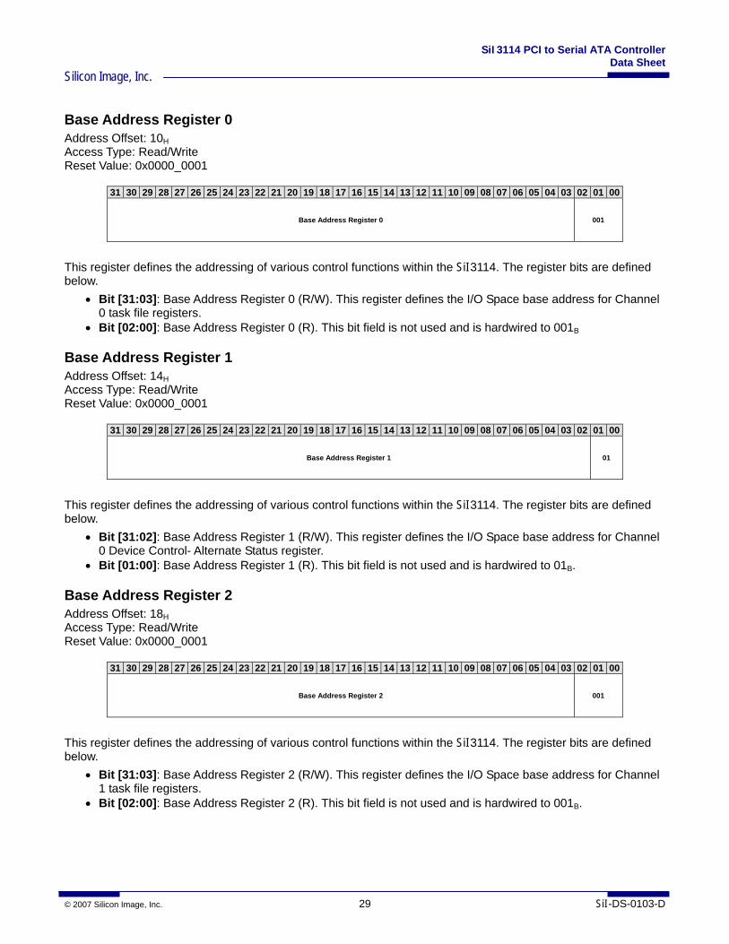
SiI3114 PCI to Serial ATA Controller Data Sheet
Silicon Image, Inc.
© 2007 Silicon Image, Inc. 29 SiI-DS-0103-D
Base Address Register 0 Address Offset: 10H Access Type: Read/Write Reset Value: 0x0000_0001
31 30 29 28 27 26 25 24 23 22 21 20 19 18 17 16 15 14 13 12 11 10 09 08 07 06 05 04 03 02 01 00
Base Address Register 0 001
This register defines the addressing of various control functions within the SiI3114. The register bits are defined below.
• Bit [31:03]: Base Address Register 0 (R/W). This register defines the I/O Space base address for Channel 0 task file registers.
• Bit [02:00]: Base Address Register 0 (R). This bit field is not used and is hardwired to 001B
Base Address Register 1 Address Offset: 14H Access Type: Read/Write Reset Value: 0x0000_0001
31 30 29 28 27 26 25 24 23 22 21 20 19 18 17 16 15 14 13 12 11 10 09 08 07 06 05 04 03 02 01 00
Base Address Register 1 01
This register defines the addressing of various control functions within the SiI3114. The register bits are defined below.
• Bit [31:02]: Base Address Register 1 (R/W). This register defines the I/O Space base address for Channel 0 Device Control- Alternate Status register.
• Bit [01:00]: Base Address Register 1 (R). This bit field is not used and is hardwired to 01B.
Base Address Register 2 Address Offset: 18H Access Type: Read/Write Reset Value: 0x0000_0001
31 30 29 28 27 26 25 24 23 22 21 20 19 18 17 16 15 14 13 12 11 10 09 08 07 06 05 04 03 02 01 00
Base Address Register 2 001
This register defines the addressing of various control functions within the SiI3114. The register bits are defined below.
• Bit [31:03]: Base Address Register 2 (R/W). This register defines the I/O Space base address for Channel 1 task file registers.
• Bit [02:00]: Base Address Register 2 (R). This bit field is not used and is hardwired to 001B.
SiI3114 PCI to Serial ATA Controller Data Sheet
Silicon Image, Inc.
SiI-DS-0103-D 30 © 2007 Silicon Image, Inc.
Base Address Register 3 Address Offset: 1CH Access Type: Read/Write Reset Value: 0x0000_0001
31 30 29 28 27 26 25 24 23 22 21 20 19 18 17 16 15 14 13 12 11 10 09 08 07 06 05 04 03 02 01 00
Base Address Register 3 01
This register defines the addressing of various control functions within the SiI3114. The register bits are defined below.
• Bit [31:02]: Base Address Register 3 (R/W). This register defines the I/O Space base address for Channel 1 Device Control- Alternate Status register.
• Bit [01:00]: Base Address Register 3 (R). This bit field is not used and is hardwired to 01B.
Base Address Register 4 Address Offset: 20H Access Type: Read/Write Reset Value: 0x0000_0001
31 30 29 28 27 26 25 24 23 22 21 20 19 18 17 16 15 14 13 12 11 10 09 08 07 06 05 04 03 02 01 00
Base Address Register 4 0001
This register defines the addressing of various control functions within the SiI3114. The register bits are defined below.
• Bit [31:04]: Base Address Register 4 (R/W). This register defines the I/O Space base address for the PCI bus master registers.
• Bit [03:00]: Base Address Register 4 (R). This bit field is not used and is hardwired to 0001B.
Base Address Register 5 Address Offset: 24H Access Type: Read/Write Reset Value: 0x0000_0000
31 30 29 28 27 26 25 24 23 22 21 20 19 18 17 16 15 14 13 12 11 10 09 08 07 06 05 04 03 02 01 00
Base Address Register 5 0000000000
This register defines the addressing of various control functions within the SiI3114. This register is enabled when input BA5_EN is set to one. See description for pin FL_ADDR[01]/BA5_EN in “Miscellaneous I/O” section on page 16 for more information. The register bits are defined below.
• Bit [31:10]: Base Address Register 5 (R/W). This register defines the Memory Space base address for all Silicon Image driver specific functions.
• Bit [09:00]: Base Address Register 5 (R). This bit field is not used and is hardwired to 000H.
SiI3114 PCI to Serial ATA Controller Data Sheet
Silicon Image, Inc.
© 2007 Silicon Image, Inc. 31 SiI-DS-0103-D
Subsystem ID – Subsystem Vendor ID Address Offset: 2CH Access Type: Read/Write Reset Value: 0x3114_1095
31 30 29 28 27 26 25 24 23 22 21 20 19 18 17 16 15 14 13 12 11 10 09 08 07 06 05 04 03 02 01 00
Subsystem ID Subsystem Vendor ID
This register defines the Subsystem ID fields associated with the PCI bus. The register bits are defined below.
• Bit [31:16]: Subsystem ID (R) – Subsystem ID. The value in this bit field is determined by any one of three options:
1) The default value of 0x3114 2) Loaded from an external memory device: If an external memory device — flash or EEPROM — is present with the correct signature, the Subsystem ID is loaded from that device after reset. See “Auto-Initialization” section on page 22 for more information. 3) System programmable: If Bit 0 of the Configuration register (40H) is set the two bytes are system programmable.
• Bit [15:00]: Subsystem Vendor ID (R) – Subsystem Vendor ID. The value in this bit field is determined by any one of three options:
1) The default value of 0x1095 2) Loaded from an external memory device : If an external memory device – Flash or EEPROM – is present with the correct signature, the Subsystem Vendor ID is loaded from that device after reset. See “Auto-Initialization” section on page 22 for more information. 3) System programmable: If Bit 0 of the Configuration register (40H) is set the two bytes are system programmable.
Expansion ROM Base Address Address Offset: 30H Access Type: Read/Write Reset Value: 0x0000_0000
31 30 29 28 27 26 25 24 23 22 21 20 19 18 17 16 15 14 13 12 11 10 09 08 07 06 05 04 03 02 01 00
Expansion ROM Base Address 000_0000_0000_0000_000
Exp
RO
M E
nabl
e
This register defines the Expansion ROM base address associated with the PCI bus. The register bits are defined below.
• Bit [31:19]: Expansion ROM Base Address (R/W) – Expansion ROM Base Address. This bit field defines the upper bits of the Expansion ROM base address.
• Bit [18:01]: Not Used (R). This bit field is hardwired to 00000H. The minimum Expansion ROM address range is 512K bytes.
• Bit [00]: Exp ROM Enable (R/W) – Expansion ROM Enable. This bit is set to enable the Expansion ROM access.
SiI3114 PCI to Serial ATA Controller Data Sheet
Silicon Image, Inc.
SiI-DS-0103-D 32 © 2007 Silicon Image, Inc.
Capabilities Pointer Address Offset: 34H Access Type: Read Reset Value: 0x0000_0060
31 30 29 28 27 26 25 24 23 22 21 20 19 18 17 16 15 14 13 12 11 10 09 08 07 06 05 04 03 02 01 00
Reserved Capabilities Pointer
This register defines the link to a list of new capabilities associated with the PCI bus. The register bits are defined below.
• Bit [31:08]: Reserved (R). This bit field is reserved and returns zeros on a read. • Bit [07:00]: Capabilities Pointer (R) – Capabilities Pointer. This bit field defaults to 60H to define the
address for the 1st entry in a list of PCI Power Management capabilities.
Max Latency – Min Grant – Interrupt Pin – Interrupt Line Address Offset: 3CH Access Type: Read/Write Reset Value: 0x0000_0100
31 30 29 28 27 26 25 24 23 22 21 20 19 18 17 16 15 14 13 12 11 10 09 08 07 06 05 04 03 02 01 00
Max Latency Min Grant Interrupt Pin Interrupt Line
This register defines the various control functions associated with the PCI bus. The register bits are defined below.
• Bit [31:24]: Max Latency (R) – Maximum Latency. This bit field is hardwired to 00H. • Bit [23:16]: Min Grant (R) – Minimum Grant. This bit field is hardwired to 00H. • Bit [15:08]: Interrupt Pin (R) – Interrupt Pin Used. This bit field is hardwired to 01H to indicate that the
SiI3114 uses the INTA# interrupt. • Bit [07:00]: Interrupt Line (R/W) – Interrupt Line. This bit field is used by the system to indicate interrupt
line routing information. The SiI3114 does not use this information.
Configuration Address Offset: 40H Access Type: Read/Write Reset Value: 0x0000_0000
31 30 29 28 27 26 25 24 23 22 21 20 19 18 17 16 15 14 13 12 11 10 09 08 07 06 05 04 03 02 01 00
Reserved
BA
5 In
d A
cc E
na
PCI H
dr W
r Ena
This register defines the various control functions associated with the PCI bus. The register bits are defined below.
• Bit [31:02]: Reserved (R). This bit field is hardwired to 00000000H.
SiI3114 PCI to Serial ATA Controller Data Sheet
Silicon Image, Inc.
© 2007 Silicon Image, Inc. 33 SiI-DS-0103-D
• Bit [01]: BA5 Ind Acc Ena (R/W) – BA5 Indirect Access Enable. This bit is set to enable indirect access to BA5 address space using Configuration Space registers C0H and C4H (BA5 Indirect Address and BA5 Indirect Access).
• Bit [00]: PCI Hdr Wr Ena (R/W) – PCI Configuration Header Write Enable. This bit is set to enable write access to the following registers in the PCI Configuration Header: Device ID (03-02H), PCI Class Code (09-0BH), Subsystem Vendor ID (2D-2CH), and Subsystem ID (2F-2EH).
Software Data Register Address Offset: 44H Access Type: Read/Write Reset Value: Undefined
31 30 29 28 27 26 25 24 23 22 21 20 19 18 17 16 15 14 13 12 11 10 09 08 07 06 05 04 03 02 01 00
Software Data
This register is used by the software for non-resettable data storage. The contents are unknown on power-up and are never cleared by any type of reset.
Power Management Capabilities Address Offset: 60H Access Type: Read Only Reset Value: 0x0622_0001
31 30 29 28 27 26 25 24 23 22 21 20 19 18 17 16 15 14 13 12 11 10 09 08 07 06 05 04 03 02 01 00
PME Support
PPM
D2
Supp
ort
PPM
D1
Supp
ort
Auxiliary Current
Dev
Spe
cial
Init
Res
erve
d
PME
Clo
ck
PPM Rev Next Item Pointer Capability ID
This register defines the power management capabilities associated with the PCI bus. The register bits are defined below.
• Bit [31:27]: PME Support (R) – Power Management Event Support. This bit field is hardwired to 00H to indicate that the SiI3114 does not support PME.
• Bit [26]: PPM D2 Support (R) – PCI Power Management D2 Support. This bit is hardwired to 1 to indicate support for the D2 Power Management State.
• Bit [25]: PPM D1 Support (R) – PCI Power Management D1 Support. This bit is hardwired to 1 to indicate support for the D1 Power Management State.
• Bit [24:22]: Auxiliary Current (R) – Auxiliary Current. This bit field is hardwired to 000B. • Bit [21]: Dev Special Init (R) – Device Special Initialization. This bit is hardwired to 1 to indicate that the
SiI3114 requires special initialization • Bit [20]: Reserved (R). This bit is reserved and returns zero on a read. • Bit [19]: PME Clock (R) – Power Management Event Clock. This bit is hardwired to 0. The SiI3114 does
not support PME. • Bit [18:16]: PPM Rev (R) – PCI Power Management Revision. This bit field is hardwired to 010B to indicate
compliance with the PCI Power Management Interface Specification revision 1.1. • Bit [15:08]: Next Item Pointer (R) – PCI Additional Capability Next Item Pointer. This bit field is hardwired to
00H to indicate that there are no additional items on the Capabilities List. • Bit [07:00]: Capability ID (R) – PCI Additional Capability ID. This bit field is hardwired to 01H to indicate that
this Capabilities List is a PCI Power Management definition.
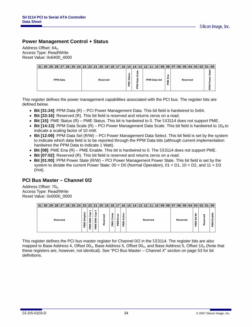
SiI3114 PCI to Serial ATA Controller Data Sheet
Silicon Image, Inc.
SiI-DS-0103-D 34 © 2007 Silicon Image, Inc.
Power Management Control + Status Address Offset: 64H Access Type: Read/Write Reset Value: 0x6400_4000
31 30 29 28 27 26 25 24 23 22 21 20 19 18 17 16 15 14 13 12 11 10 09 08 07 06 05 04 03 02 01 00
PPM Data Reserved
PME
Stat
us
PPM
Dat
a Sc
ale
PPM Data Sel
PME
Ena
Reserved
PPM
Pow
er S
tate
This register defines the power management capabilities associated with the PCI bus. The register bits are defined below.
• Bit [31:24]: PPM Data (R) – PCI Power Management Data. This bit field is hardwired to 0x64. • Bit [23:16]: Reserved (R). This bit field is reserved and returns zeros on a read. • Bit [15]: PME Status (R) – PME Status. This bit is hardwired to 0. The SiI3114 does not support PME. • Bit [14:13]: PPM Data Scale (R) – PCI Power Management Data Scale. This bit field is hardwired to 10B to
indicate a scaling factor of 10 mW. • Bit [12:09]: PPM Data Sel (R/W) – PCI Power Management Data Select. This bit field is set by the system
to indicate which data field is to be reported through the PPM Data bits (although current implementation hardwires the PPM Data to indicate 1 Watt).
• Bit [08]: PME Ena (R) – PME Enable. This bit is hardwired to 0. The SiI3114 does not support PME. • Bit [07:02]: Reserved (R). This bit field is reserved and returns zeros on a read. • Bit [01:00]: PPM Power State (R/W) – PCI Power Management Power State. This bit field is set by the
system to dictate the current Power State: 00 = D0 (Normal Operation), 01 = D1, 10 = D2, and 11 = D3 (Hot).
PCI Bus Master – Channel 0/2 Address Offset: 70H Access Type: Read/Write Reset Value: 0x0000_0000
31 30 29 28 27 26 25 24 23 22 21 20 19 18 17 16 15 14 13 12 11 10 09 08 07 06 05 04 03 02 01 00
Reserved
PBM
Sim
plex
PBM
DM
A C
ap 1
PBM
DM
A C
ap 0
Res
erve
d
DM
A C
omp
PBM
Err
or
PBM
Act
ive
Reserved Reserved
PBM
Rd-
Wr
Res
erve
d
PBM
Ena
ble
This register defines the PCI bus master register for Channel 0/2 in the SiI3114. The register bits are also mapped to Base Address 4, Offset 00H, Base Address 5, Offset 00H, and Base Address 5, Offset 10H (Note that these registers are, however, not identical). See “PCI Bus Master – Channel X” section on page 53 for bit definitions.
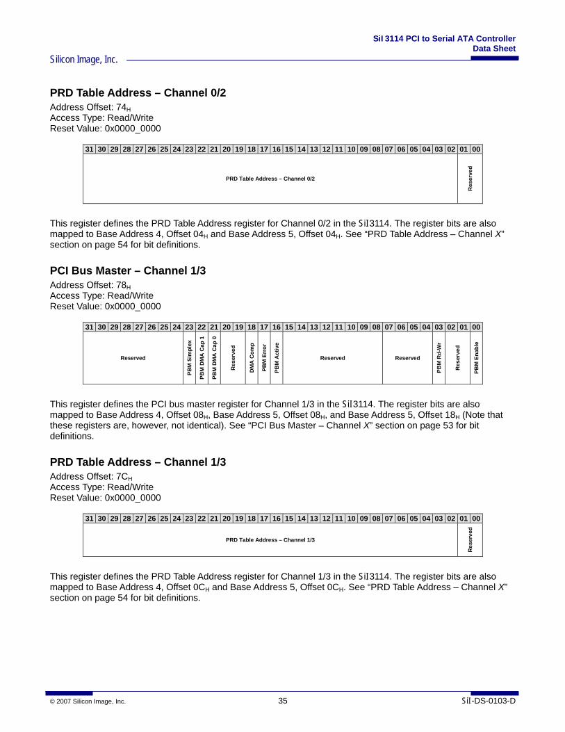
SiI3114 PCI to Serial ATA Controller Data Sheet
Silicon Image, Inc.
© 2007 Silicon Image, Inc. 35 SiI-DS-0103-D
PRD Table Address – Channel 0/2 Address Offset: 74H Access Type: Read/Write Reset Value: 0x0000_0000
31 30 29 28 27 26 25 24 23 22 21 20 19 18 17 16 15 14 13 12 11 10 09 08 07 06 05 04 03 02 01 00
PRD Table Address – Channel 0/2
Res
erve
d
This register defines the PRD Table Address register for Channel 0/2 in the SiI3114. The register bits are also mapped to Base Address 4, Offset 04H and Base Address 5, Offset 04H. See “PRD Table Address – Channel X” section on page 54 for bit definitions.
PCI Bus Master – Channel 1/3 Address Offset: 78H Access Type: Read/Write Reset Value: 0x0000_0000
31 30 29 28 27 26 25 24 23 22 21 20 19 18 17 16 15 14 13 12 11 10 09 08 07 06 05 04 03 02 01 00
Reserved
PBM
Sim
plex
PBM
DM
A C
ap 1
PBM
DM
A C
ap 0
Res
erve
d
DM
A C
omp
PBM
Err
or
PBM
Act
ive
Reserved Reserved
PBM
Rd-
Wr
Res
erve
d
PBM
Ena
ble
This register defines the PCI bus master register for Channel 1/3 in the SiI3114. The register bits are also mapped to Base Address 4, Offset 08H, Base Address 5, Offset 08H, and Base Address 5, Offset 18H (Note that these registers are, however, not identical). See “PCI Bus Master – Channel X” section on page 53 for bit definitions.
PRD Table Address – Channel 1/3 Address Offset: 7CH Access Type: Read/Write Reset Value: 0x0000_0000
31 30 29 28 27 26 25 24 23 22 21 20 19 18 17 16 15 14 13 12 11 10 09 08 07 06 05 04 03 02 01 00
PRD Table Address – Channel 1/3
Res
erve
d
This register defines the PRD Table Address register for Channel 1/3 in the SiI3114. The register bits are also mapped to Base Address 4, Offset 0CH and Base Address 5, Offset 0CH. See “PRD Table Address – Channel X” section on page 54 for bit definitions.
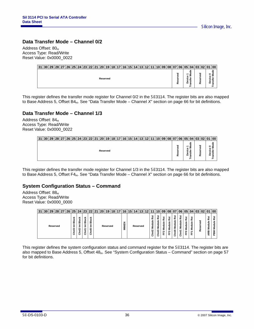
SiI3114 PCI to Serial ATA Controller Data Sheet
Silicon Image, Inc.
SiI-DS-0103-D 36 © 2007 Silicon Image, Inc.
Data Transfer Mode – Channel 0/2 Address Offset: 80H Access Type: Read/Write Reset Value: 0x0000_0022
31 30 29 28 27 26 25 24 23 22 21 20 19 18 17 16 15 14 13 12 11 10 09 08 07 06 05 04 03 02 01 00
Reserved
Res
erve
d
Dev
ice
1
Tran
sfer
Mod
e
Res
erve
d
Dev
ice
0
Tran
sfer
Mod
e
This register defines the transfer mode register for Channel 0/2 in the SiI3114. The register bits are also mapped to Base Address 5, Offset B4H. See “Data Transfer Mode – Channel X” section on page 66 for bit definitions.
Data Transfer Mode – Channel 1/3 Address Offset: 84H Access Type: Read/Write Reset Value: 0x0000_0022
31 30 29 28 27 26 25 24 23 22 21 20 19 18 17 16 15 14 13 12 11 10 09 08 07 06 05 04 03 02 01 00
Reserved
Res
erve
d
Dev
ice
1
Tran
sfer
Mod
e
Res
erve
d
Dev
ice
0
Tran
sfer
Mod
e
This register defines the transfer mode register for Channel 1/3 in the SiI3114. The register bits are also mapped to Base Address 5, Offset F4H. See “Data Transfer Mode – Channel X” section on page 66 for bit definitions.
System Configuration Status – Command Address Offset: 88H Access Type: Read/Write Reset Value: 0x0000_0000
31 30 29 28 27 26 25 24 23 22 21 20 19 18 17 16 15 14 13 12 11 10 09 08 07 06 05 04 03 02 01 00
Reserved
Chn
l3 In
t Blo
ck
Chn
l2 In
t Blo
ck
Chn
l1 In
t Blo
ck
Chn
l0 In
t Blo
ck
Reserved
M66
EN
Reserved
Chn
l2 M
odul
e R
st
Chn
l3 M
odul
e R
st
FF2
Mod
ule
Rst
FF3
Mod
ule
Rst
Chn
l0 M
odul
e R
st
Chn
l1 M
odul
e R
st
FF0
Mod
ule
Rst
FF1
Mod
ule
Rst
Res
erve
d
AR
B M
odul
e R
st
PBM
Mod
ule
Rst
This register defines the system configuration status and command register for the SiI3114. The register bits are also mapped to Base Address 5, Offset 48H. See “System Configuration Status – Command” section on page 57 for bit definitions.
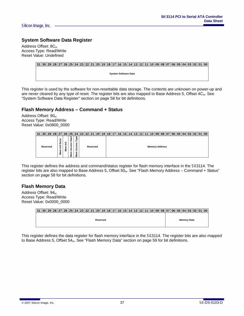
SiI3114 PCI to Serial ATA Controller Data Sheet
Silicon Image, Inc.
© 2007 Silicon Image, Inc. 37 SiI-DS-0103-D
System Software Data Register Address Offset: 8CH Access Type: Read/Write Reset Value: Undefined
31 30 29 28 27 26 25 24 23 22 21 20 19 18 17 16 15 14 13 12 11 10 09 08 07 06 05 04 03 02 01 00
System Software Data
This register is used by the software for non-resettable data storage. The contents are unknown on power-up and are never cleared by any type of reset. The register bits are also mapped to Base Address 5, Offset 4CH. See “System Software Data Register” section on page 58 for bit definitions.
Flash Memory Address – Command + Status Address Offset: 90H Access Type: Read/Write Reset Value: 0x0800_0000
31 30 29 28 27 26 25 24 23 22 21 20 19 18 17 16 15 14 13 12 11 10 09 08 07 06 05 04 03 02 01 00
Reserved
Mem
Init
Don
e
Mem
Init
Mem
Acc
ess
Star
t
Mem
Acc
ess
Type
Reserved Memory Address
This register defines the address and command/status register for flash memory interface in the SiI3114. The register bits are also mapped to Base Address 5, Offset 50H. See “Flash Memory Address – Command + Status” section on page 58 for bit definitions.
Flash Memory Data Address Offset: 94H Access Type: Read/Write Reset Value: 0x0000_0000
31 30 29 28 27 26 25 24 23 22 21 20 19 18 17 16 15 14 13 12 11 10 09 08 07 06 05 04 03 02 01 00
Reserved Memory Data
This register defines the data register for flash memory interface in the SiI3114. The register bits are also mapped to Base Address 5, Offset 54H. See “Flash Memory Data” section on page 59 for bit definitions.
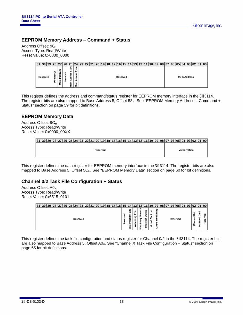
SiI3114 PCI to Serial ATA Controller Data Sheet
Silicon Image, Inc.
SiI-DS-0103-D 38 © 2007 Silicon Image, Inc.
EEPROM Memory Address – Command + Status Address Offset: 98H Access Type: Read/Write Reset Value: 0x0800_0000
31 30 29 28 27 26 25 24 23 22 21 20 19 18 17 16 15 14 13 12 11 10 09 08 07 06 05 04 03 02 01 00
Reserved
Mem
Err
or
Mem
Init
Don
e
Mem
Init
Mem
Acc
ess
Star
t
Mem
Acc
ess
Type
Reserved Mem Address
This register defines the address and command/status register for EEPROM memory interface in the SiI3114. The register bits are also mapped to Base Address 5, Offset 58H. See “EEPROM Memory Address – Command + Status” section on page 59 for bit definitions.
EEPROM Memory Data Address Offset: 9CH Access Type: Read/Write Reset Value: 0x0000_00XX
31 30 29 28 27 26 25 24 23 22 21 20 19 18 17 16 15 14 13 12 11 10 09 08 07 06 05 04 03 02 01 00
Reserved Memory Data
This register defines the data register for EEPROM memory interface in the SiI3114. The register bits are also mapped to Base Address 5, Offset 5CH. See “EEPROM Memory Data” section on page 60 for bit definitions.
Channel 0/2 Task File Configuration + Status Address Offset: A0H Access Type: Read/Write Reset Value: 0x6515_0101
31 30 29 28 27 26 25 24 23 22 21 20 19 18 17 16 15 14 13 12 11 10 09 08 07 06 05 04 03 02 01 00
Reserved
Res
erve
d
Wat
chdo
g In
t Ena
Wat
chdo
g En
a
Wat
chdo
g Ti
meo
ut
Inte
rrup
t Sta
tus
Virt
ual D
MA
Int
IOR
DY
Mon
itorin
g
Reserved
Cha
nnel
Rst
Buf
fere
d C
md
Res
erve
d
This register defines the task file configuration and status register for Channel 0/2 in the SiI3114. The register bits are also mapped to Base Address 5, Offset A0H. See “Channel X Task File Configuration + Status” section on page 65 for bit definitions.
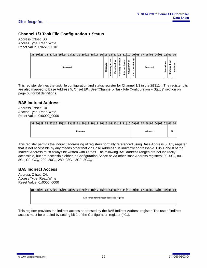
SiI3114 PCI to Serial ATA Controller Data Sheet
Silicon Image, Inc.
© 2007 Silicon Image, Inc. 39 SiI-DS-0103-D
Channel 1/3 Task File Configuration + Status Address Offset: B0H Access Type: Read/Write Reset Value: 0x6515_0101
31 30 29 28 27 26 25 24 23 22 21 20 19 18 17 16 15 14 13 12 11 10 09 08 07 06 05 04 03 02 01 00
Reserved
Res
erve
d
Wat
chdo
g In
t Ena
Wat
chdo
g En
a
Wat
chdo
g Ti
meo
ut
Inte
rrup
t Sta
tus
Virt
ual D
MA
Int
IOR
DY
Mon
itorin
g
Reserved
Cha
nnel
Rst
Buf
fere
d C
md
Res
erve
d
This register defines the task file configuration and status register for Channel 1/3 in the SiI3114. The register bits are also mapped to Base Address 5, Offset E0H.See “Channel X Task File Configuration + Status” section on page 65 for bit definitions.
BA5 Indirect Address Address Offset: C0H Access Type: Read/Write Reset Value: 0x0000_0000
31 30 29 28 27 26 25 24 23 22 21 20 19 18 17 16 15 14 13 12 11 10 09 08 07 06 05 04 03 02 01 00
Reserved Address 00
This register permits the indirect addressing of registers normally referenced using Base Address 5. Any register that is not accessible by any means other that via Base Address 5 is indirectly addressable. Bits 1 and 0 of the Indirect Address must always be written with zeroes. The following BA5 address ranges are not indirectly accessible, but are accessible either in Configuration Space or via other Base Address registers: 00–0CH, 80–8CH, C0–CCH, 200–20CH, 280–28CH, 2C0–2CCH.
BA5 Indirect Access Address Offset: C4H Access Type: Read/Write Reset Value: 0x0000_0000
31 30 29 28 27 26 25 24 23 22 21 20 19 18 17 16 15 14 13 12 11 10 09 08 07 06 05 04 03 02 01 00
As defined for indirectly accessed register
This register provides the indirect access addressed by the BA5 Indirect Address register. The use of indirect access must be enabled by setting bit 1 of the Configuration register (40H).
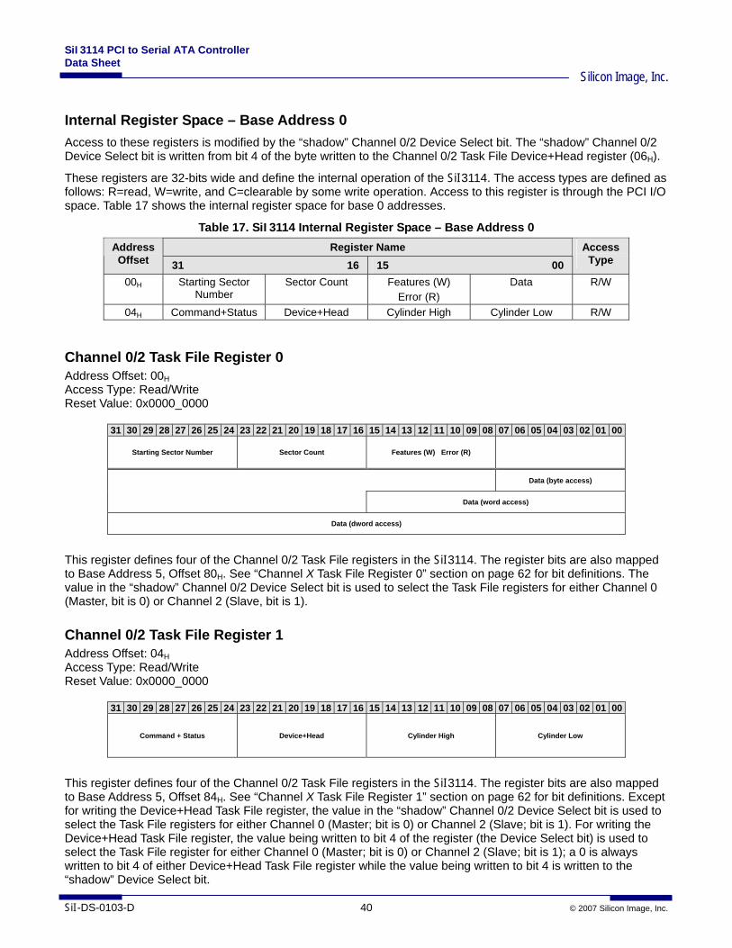
SiI3114 PCI to Serial ATA Controller Data Sheet
Silicon Image, Inc.
SiI-DS-0103-D 40 © 2007 Silicon Image, Inc.
Internal Register Space – Base Address 0 Access to these registers is modified by the “shadow” Channel 0/2 Device Select bit. The “shadow” Channel 0/2 Device Select bit is written from bit 4 of the byte written to the Channel 0/2 Task File Device+Head register (06H).
These registers are 32-bits wide and define the internal operation of the SiI3114. The access types are defined as follows: R=read, W=write, and C=clearable by some write operation. Access to this register is through the PCI I/O space. Table 17 shows the internal register space for base 0 addresses.
Table 17. SiI3114 Internal Register Space – Base Address 0 Register Name Address
Offset 31 16 15 00 Access
Type
00H Starting Sector Number
Sector Count Features (W) Error (R)
Data R/W
04H Command+Status Device+Head Cylinder High Cylinder Low R/W
Channel 0/2 Task File Register 0 Address Offset: 00H Access Type: Read/Write Reset Value: 0x0000_0000
31 30 29 28 27 26 25 24 23 22 21 20 19 18 17 16 15 14 13 12 11 10 09 08 07 06 05 04 03 02 01 00
Starting Sector Number Sector Count Features (W) Error (R)
Data (byte access)
Data (word access)
Data (dword access)
This register defines four of the Channel 0/2 Task File registers in the SiI3114. The register bits are also mapped to Base Address 5, Offset 80H. See “Channel X Task File Register 0” section on page 62 for bit definitions. The value in the “shadow” Channel 0/2 Device Select bit is used to select the Task File registers for either Channel 0 (Master, bit is 0) or Channel 2 (Slave, bit is 1).
Channel 0/2 Task File Register 1 Address Offset: 04H Access Type: Read/Write Reset Value: 0x0000_0000
31 30 29 28 27 26 25 24 23 22 21 20 19 18 17 16 15 14 13 12 11 10 09 08 07 06 05 04 03 02 01 00
Command + Status Device+Head Cylinder High Cylinder Low
This register defines four of the Channel 0/2 Task File registers in the SiI3114. The register bits are also mapped to Base Address 5, Offset 84H. See “Channel X Task File Register 1” section on page 62 for bit definitions. Except for writing the Device+Head Task File register, the value in the “shadow” Channel 0/2 Device Select bit is used to select the Task File registers for either Channel 0 (Master; bit is 0) or Channel 2 (Slave; bit is 1). For writing the Device+Head Task File register, the value being written to bit 4 of the register (the Device Select bit) is used to select the Task File register for either Channel 0 (Master; bit is 0) or Channel 2 (Slave; bit is 1); a 0 is always written to bit 4 of either Device+Head Task File register while the value being written to bit 4 is written to the “shadow” Device Select bit.
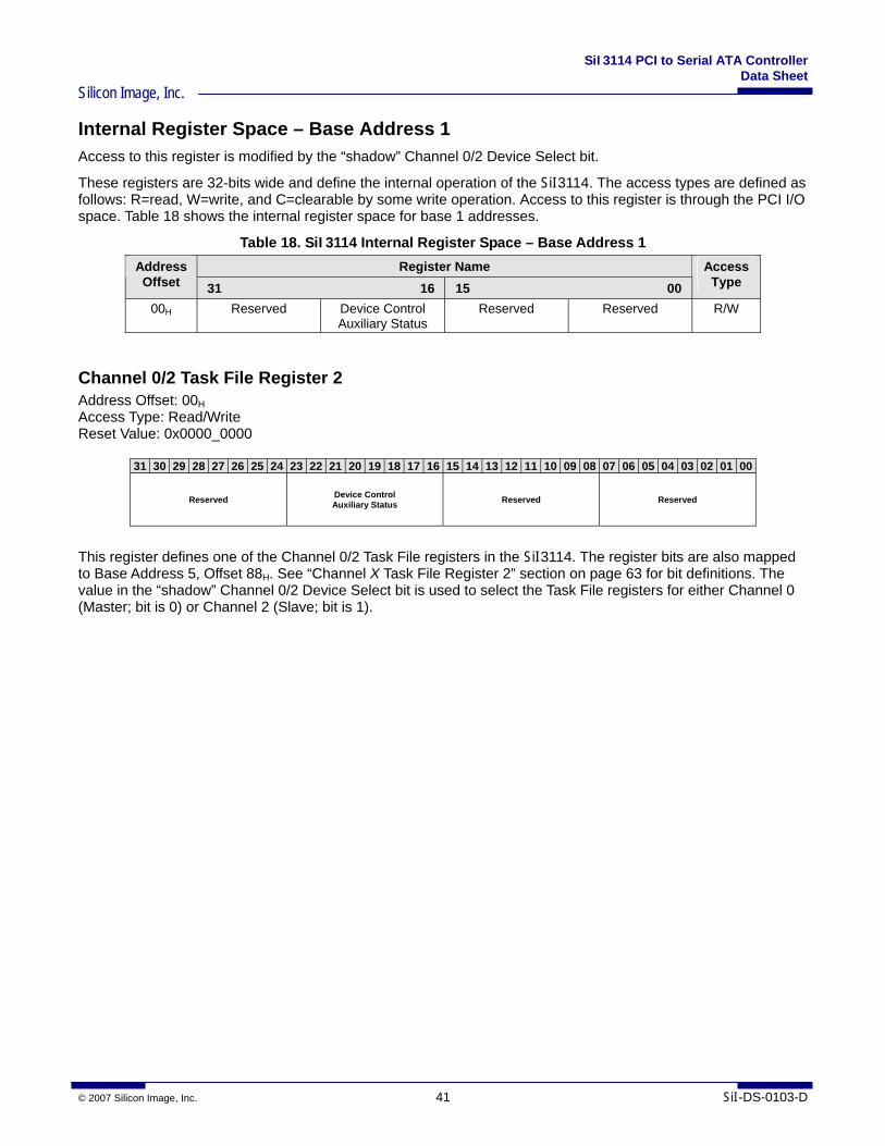
SiI3114 PCI to Serial ATA Controller Data Sheet
Silicon Image, Inc.
© 2007 Silicon Image, Inc. 41 SiI-DS-0103-D
Internal Register Space – Base Address 1 Access to this register is modified by the “shadow” Channel 0/2 Device Select bit.
These registers are 32-bits wide and define the internal operation of the SiI3114. The access types are defined as follows: R=read, W=write, and C=clearable by some write operation. Access to this register is through the PCI I/O space. Table 18 shows the internal register space for base 1 addresses.
Table 18. SiI3114 Internal Register Space – Base Address 1 Register Name Address
Offset 31 16 15 00 Access
Type
00H Reserved Device Control Auxiliary Status
Reserved Reserved R/W
Channel 0/2 Task File Register 2 Address Offset: 00H Access Type: Read/Write Reset Value: 0x0000_0000
31 30 29 28 27 26 25 24 23 22 21 20 19 18 17 16 15 14 13 12 11 10 09 08 07 06 05 04 03 02 01 00
Reserved Device Control Auxiliary Status Reserved Reserved
This register defines one of the Channel 0/2 Task File registers in the SiI3114. The register bits are also mapped to Base Address 5, Offset 88H. See “Channel X Task File Register 2” section on page 63 for bit definitions. The value in the “shadow” Channel 0/2 Device Select bit is used to select the Task File registers for either Channel 0 (Master; bit is 0) or Channel 2 (Slave; bit is 1).
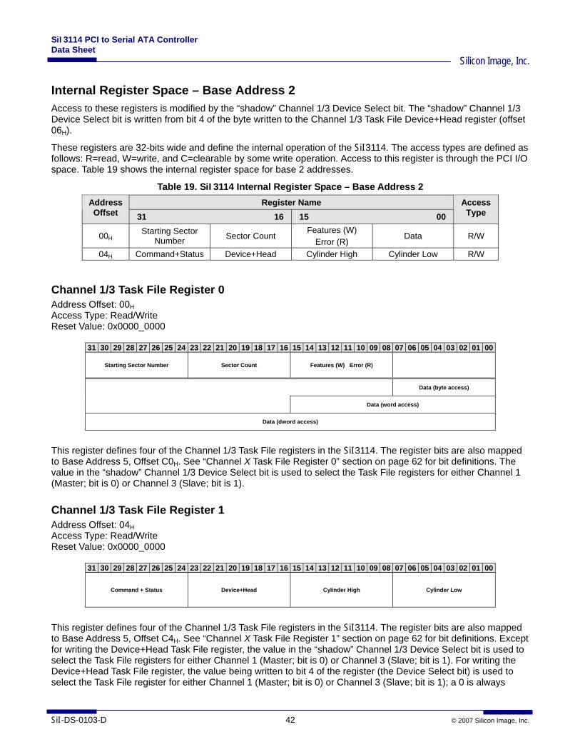
SiI3114 PCI to Serial ATA Controller Data Sheet
Silicon Image, Inc.
SiI-DS-0103-D 42 © 2007 Silicon Image, Inc.
Internal Register Space – Base Address 2 Access to these registers is modified by the “shadow” Channel 1/3 Device Select bit. The “shadow” Channel 1/3 Device Select bit is written from bit 4 of the byte written to the Channel 1/3 Task File Device+Head register (offset 06H).
These registers are 32-bits wide and define the internal operation of the SiI3114. The access types are defined as follows: R=read, W=write, and C=clearable by some write operation. Access to this register is through the PCI I/O space. Table 19 shows the internal register space for base 2 addresses.
Table 19. SiI3114 Internal Register Space – Base Address 2 Register Name Address
Offset 31 16 15 00 Access
Type
00H Starting Sector Number Sector Count
Features (W) Error (R)
Data R/W
04H Command+Status Device+Head Cylinder High Cylinder Low R/W
Channel 1/3 Task File Register 0 Address Offset: 00H Access Type: Read/Write Reset Value: 0x0000_0000
31 30 29 28 27 26 25 24 23 22 21 20 19 18 17 16 15 14 13 12 11 10 09 08 07 06 05 04 03 02 01 00
Starting Sector Number Sector Count Features (W) Error (R)
Data (byte access)
Data (word access)
Data (dword access)
This register defines four of the Channel 1/3 Task File registers in the SiI3114. The register bits are also mapped to Base Address 5, Offset C0H. See “Channel X Task File Register 0” section on page 62 for bit definitions. The value in the “shadow” Channel 1/3 Device Select bit is used to select the Task File registers for either Channel 1 (Master; bit is 0) or Channel 3 (Slave; bit is 1).
Channel 1/3 Task File Register 1 Address Offset: 04H Access Type: Read/Write Reset Value: 0x0000_0000
31 30 29 28 27 26 25 24 23 22 21 20 19 18 17 16 15 14 13 12 11 10 09 08 07 06 05 04 03 02 01 00
Command + Status Device+Head Cylinder High Cylinder Low
This register defines four of the Channel 1/3 Task File registers in the SiI3114. The register bits are also mapped to Base Address 5, Offset C4H. See “Channel X Task File Register 1” section on page 62 for bit definitions. Except for writing the Device+Head Task File register, the value in the “shadow” Channel 1/3 Device Select bit is used to select the Task File registers for either Channel 1 (Master; bit is 0) or Channel 3 (Slave; bit is 1). For writing the Device+Head Task File register, the value being written to bit 4 of the register (the Device Select bit) is used to select the Task File register for either Channel 1 (Master; bit is 0) or Channel 3 (Slave; bit is 1); a 0 is always
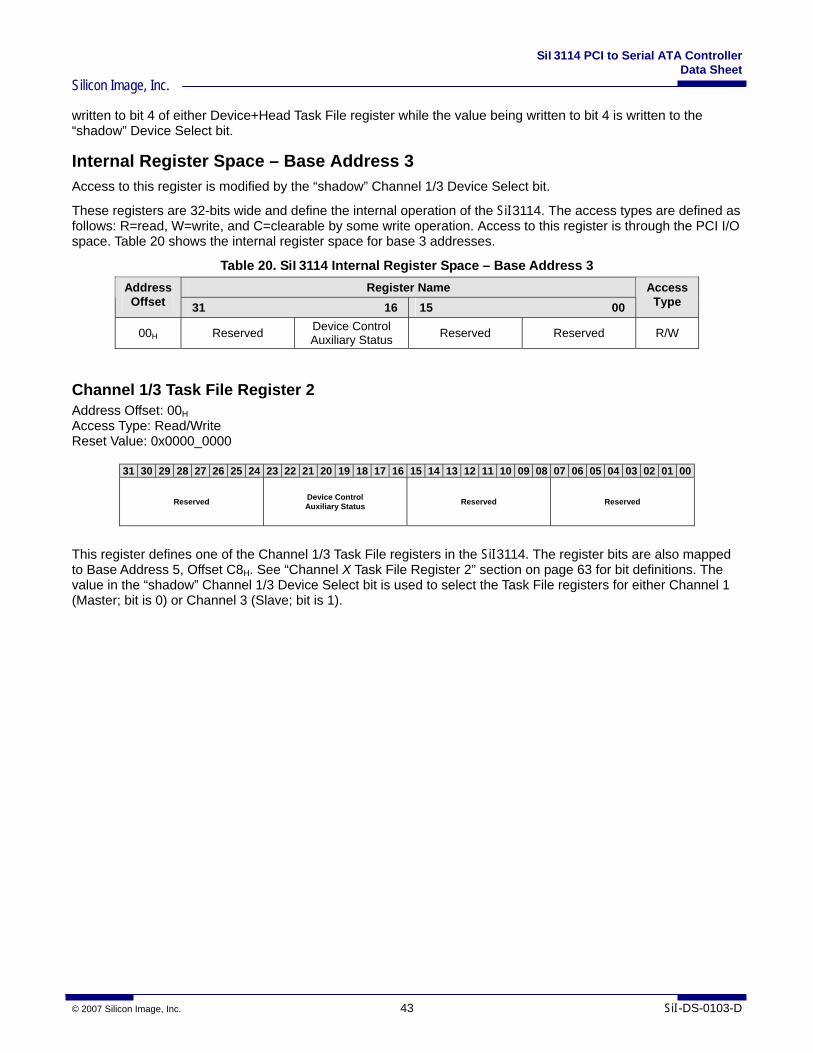
SiI3114 PCI to Serial ATA Controller Data Sheet
Silicon Image, Inc.
© 2007 Silicon Image, Inc. 43 SiI-DS-0103-D
written to bit 4 of either Device+Head Task File register while the value being written to bit 4 is written to the “shadow” Device Select bit.
Internal Register Space – Base Address 3 Access to this register is modified by the “shadow” Channel 1/3 Device Select bit.
These registers are 32-bits wide and define the internal operation of the SiI3114. The access types are defined as follows: R=read, W=write, and C=clearable by some write operation. Access to this register is through the PCI I/O space. Table 20 shows the internal register space for base 3 addresses.
Table 20. SiI3114 Internal Register Space – Base Address 3 Register Name Address
Offset 31 16 15 00 Access
Type
00H Reserved Device Control Auxiliary Status Reserved Reserved R/W
Channel 1/3 Task File Register 2 Address Offset: 00H Access Type: Read/Write Reset Value: 0x0000_0000
31 30 29 28 27 26 25 24 23 22 21 20 19 18 17 16 15 14 13 12 11 10 09 08 07 06 05 04 03 02 01 00
Reserved Device Control Auxiliary Status Reserved Reserved
This register defines one of the Channel 1/3 Task File registers in the SiI3114. The register bits are also mapped to Base Address 5, Offset C8H. See “Channel X Task File Register 2” section on page 63 for bit definitions. The value in the “shadow” Channel 1/3 Device Select bit is used to select the Task File registers for either Channel 1 (Master; bit is 0) or Channel 3 (Slave; bit is 1).
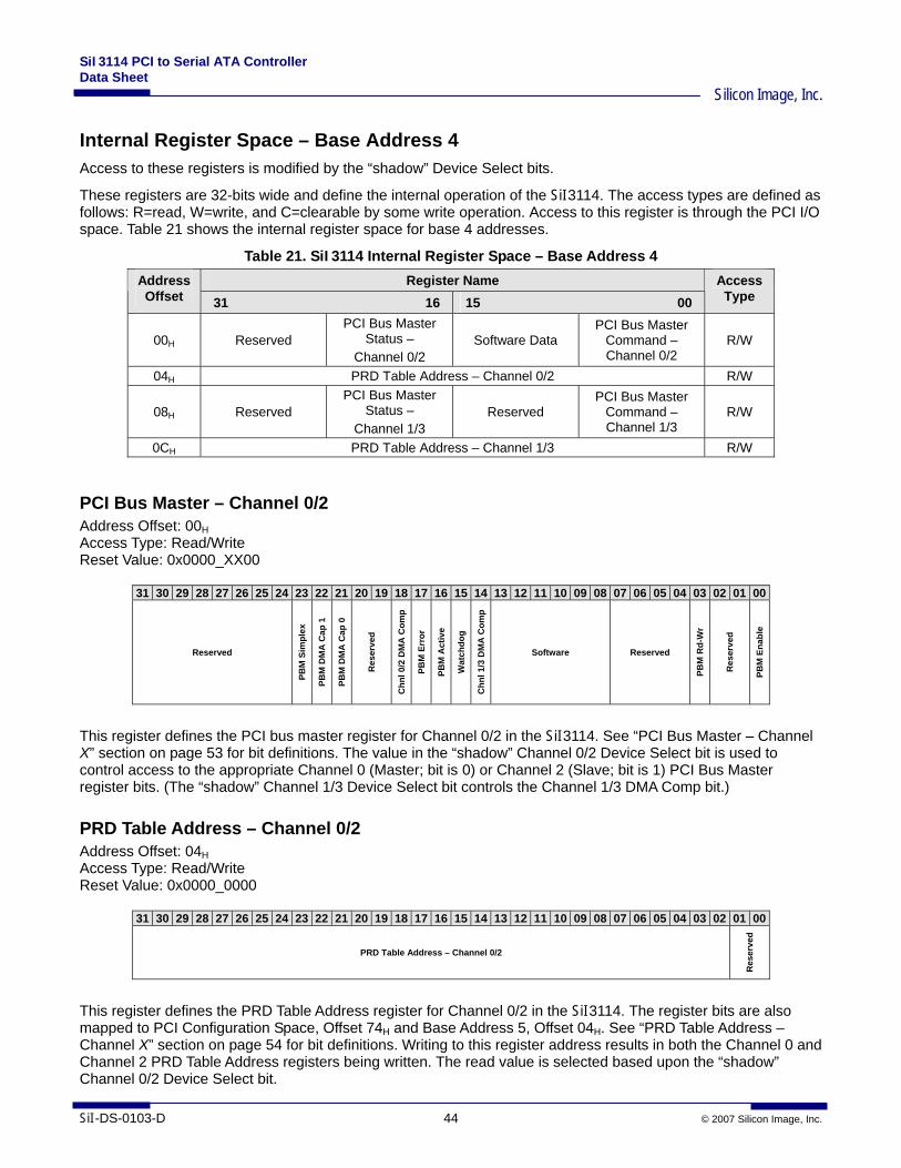
SiI3114 PCI to Serial ATA Controller Data Sheet
Silicon Image, Inc.
SiI-DS-0103-D 44 © 2007 Silicon Image, Inc.
Internal Register Space – Base Address 4 Access to these registers is modified by the “shadow” Device Select bits.
These registers are 32-bits wide and define the internal operation of the SiI3114. The access types are defined as follows: R=read, W=write, and C=clearable by some write operation. Access to this register is through the PCI I/O space. Table 21 shows the internal register space for base 4 addresses.
Table 21. SiI3114 Internal Register Space – Base Address 4 Register Name Address
Offset 31 16 15 00 Access
Type
00H Reserved PCI Bus Master
Status – Channel 0/2
Software Data PCI Bus Master
Command – Channel 0/2
R/W
04H PRD Table Address – Channel 0/2 R/W
08H Reserved PCI Bus Master
Status – Channel 1/3
Reserved PCI Bus Master
Command – Channel 1/3
R/W
0CH PRD Table Address – Channel 1/3 R/W
PCI Bus Master – Channel 0/2 Address Offset: 00H Access Type: Read/Write Reset Value: 0x0000_XX00
31 30 29 28 27 26 25 24 23 22 21 20 19 18 17 16 15 14 13 12 11 10 09 08 07 06 05 04 03 02 01 00
Reserved
PBM
Sim
plex
PBM
DM
A C
ap 1
PBM
DM
A C
ap 0
Res
erve
d
Chn
l 0/2
DM
A C
omp
PBM
Err
or
PBM
Act
ive
Wat
chdo
g
Chn
l 1/3
DM
A C
omp
Software Reserved
PBM
Rd-
Wr
Res
erve
d
PBM
Ena
ble
This register defines the PCI bus master register for Channel 0/2 in the SiI3114. See “PCI Bus Master – Channel X” section on page 53 for bit definitions. The value in the “shadow” Channel 0/2 Device Select bit is used to control access to the appropriate Channel 0 (Master; bit is 0) or Channel 2 (Slave; bit is 1) PCI Bus Master register bits. (The “shadow” Channel 1/3 Device Select bit controls the Channel 1/3 DMA Comp bit.)
PRD Table Address – Channel 0/2 Address Offset: 04H Access Type: Read/Write Reset Value: 0x0000_0000
31 30 29 28 27 26 25 24 23 22 21 20 19 18 17 16 15 14 13 12 11 10 09 08 07 06 05 04 03 02 01 00
PRD Table Address – Channel 0/2
Res
erve
d
This register defines the PRD Table Address register for Channel 0/2 in the SiI3114. The register bits are also mapped to PCI Configuration Space, Offset 74H and Base Address 5, Offset 04H. See “PRD Table Address – Channel X” section on page 54 for bit definitions. Writing to this register address results in both the Channel 0 and Channel 2 PRD Table Address registers being written. The read value is selected based upon the “shadow” Channel 0/2 Device Select bit.
SiI3114 PCI to Serial ATA Controller Data Sheet
Silicon Image, Inc.
© 2007 Silicon Image, Inc. 45 SiI-DS-0103-D
PCI Bus Master – Channel 1/3 Address Offset: 08H Access Type: Read/Write Reset Value: 0x0000_0000
31 30 29 28 27 26 25 24 23 22 21 20 19 18 17 16 15 14 13 12 11 10 09 08 07 06 05 04 03 02 01 00
Reserved
PBM
Sim
plex
PBM
DM
A C
ap 1
PBM
DM
A C
ap 0
Res
erve
d
Chn
l 1/3
DM
A C
omp
PBM
Err
or
PBM
Act
ive
Reserved Reserved
PBM
Rd-
Wr
Res
erve
d
PBM
Ena
ble
This register defines the PCI bus master register for Channel 1/3 in the SiI3114. See “PRD Table Address – Channel X” section on page 54 for bit definitions. The value in the “shadow” Channel 1/3 Device Select bit is used to control access to the appropriate Channel 1 (Master; bit is 0) or Channel 3 (Slave; bit is 1) PCI Bus Master register bits.
PRD Table Address – Channel 1/3 Address Offset: 0CH Access Type: Read/Write Reset Value: 0x0000_0000
31 30 29 28 27 26 25 24 23 22 21 20 19 18 17 16 15 14 13 12 11 10 09 08 07 06 05 04 03 02 01 00
PRD Table Address – Channel 1/3
Res
erve
d
This register defines the PRD Table Address register for Channel 1/3 in the SiI3114. The register bits are also mapped to PCI Configuration Space, Offset 7CH and Base Address 5, Offset 0CH. See “PRD Table Address – Channel X” section on page 54 for bit definitions. Writing to this register address results in both the Channel 1 and Channel 3 PRD Table Address registers being written. The read value is selected based upon the “shadow” Channel 1/3 Device Select bit.
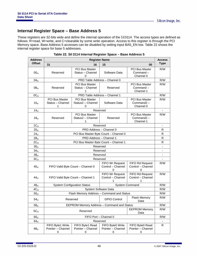
SiI3114 PCI to Serial ATA Controller Data Sheet
Silicon Image, Inc.
SiI-DS-0103-D 46 © 2007 Silicon Image, Inc.
Internal Register Space – Base Address 5 These registers are 32-bits wide and define the internal operation of the SiI3114. The access types are defined as follows: R=read, W=write, and C=clearable by some write operation. Access to this register is through the PCI Memory space. Base Address 5 accesses can be disabled by setting input BA5_EN low. Table 22 shows the internal register space for base 5 addresses.
Table 22. SiI3114 Internal Register Space – Base Address 5 Register Name Address
Offset 31 16 15 00 Access
Type
00H Reserved PCI Bus Master
Status – Channel 0
Software Data PCI Bus Master
Command – Channel 0
R/W
04H PRD Table Address – Channel 0 R/W
08H Reserved PCI Bus Master
Status – Channel 1
Reserved PCI Bus Master
Command – Channel 1
R/W
0CH PRD Table Address – Channel 1 R/W
10H PCI Bus Master
Status – Channel 1
PCI Bus Master Status2 – Channel
0 Software Data
PCI Bus Master Command2 –
Channel 0
R/W
14H Reserved -
18H Reserved PCI Bus Master
Status2 – Channel 1
Reserved PCI Bus Master Command2 –
Channel 1
R/W
1CH Reserved - 20H PRD Address – Channel 0 R 24H PCI Bus Master Byte Count – Channel 0 R 28H PRD Address – Channel 1 R 2CH PCI Bus Master Byte Count – Channel 1 R 30H Reserved - 34H Reserved - 38H Reserved - 3CH Reserved -
40H FIFO Valid Byte Count – Channel 0 FIFO Wr Request Control – Channel
0
FIFO Rd Request Control – Channel
0
R/W
44H FIFO Valid Byte Count – Channel 1 FIFO Wr Request Control – Channel
1
FIFO Rd Request Control – Channel
1
R/W
48H System Configuration Status System Command R/W 4CH System Software Data R/W 50H Flash Memory Address – Command and Status R/W
54H Reserved GPIO Control Flash Memory Data
R/W
58H EEPROM Memory Address – Command and Status R/W
5CH Reserved EEPROM Memory Data
R/W
60H FIFO Port – Channel 0 R/W 64H Reserved -
68H FIFO Byte1 Write Pointer – Channel
0
FIFO Byte1 Read Pointer – Channel
0
FIFO Byte0 Write Pointer – Channel
0
FIFO Byte0 Read Pointer – Channel
0
R
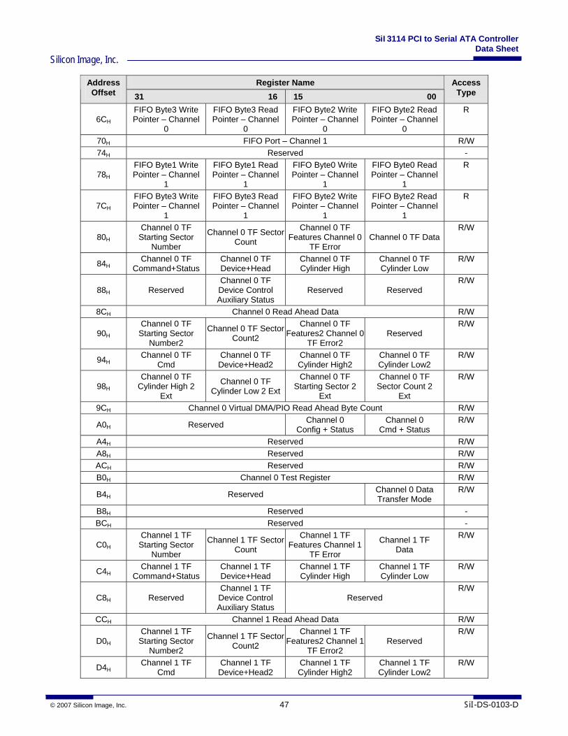
SiI3114 PCI to Serial ATA Controller Data Sheet
Silicon Image, Inc.
© 2007 Silicon Image, Inc. 47 SiI-DS-0103-D
Register Name Address Offset 31 16 15 00
Access Type
6CH FIFO Byte3 Write Pointer – Channel
0
FIFO Byte3 Read Pointer – Channel
0
FIFO Byte2 Write Pointer – Channel
0
FIFO Byte2 Read Pointer – Channel
0
R
70H FIFO Port – Channel 1 R/W 74H Reserved -
78H FIFO Byte1 Write Pointer – Channel
1
FIFO Byte1 Read Pointer – Channel
1
FIFO Byte0 Write Pointer – Channel
1
FIFO Byte0 Read Pointer – Channel
1
R
7CH FIFO Byte3 Write Pointer – Channel
1
FIFO Byte3 Read Pointer – Channel
1
FIFO Byte2 Write Pointer – Channel
1
FIFO Byte2 Read Pointer – Channel
1
R
80H Channel 0 TF Starting Sector
Number
Channel 0 TF Sector Count
Channel 0 TF Features Channel 0
TF Error Channel 0 TF Data
R/W
84H Channel 0 TF Command+Status
Channel 0 TF Device+Head
Channel 0 TF Cylinder High
Channel 0 TF Cylinder Low
R/W
88H Reserved Channel 0 TF Device Control Auxiliary Status
Reserved Reserved R/W
8CH Channel 0 Read Ahead Data R/W
90H Channel 0 TF Starting Sector
Number2
Channel 0 TF Sector Count2
Channel 0 TF Features2 Channel 0
TF Error2 Reserved
R/W
94H Channel 0 TF Cmd
Channel 0 TF Device+Head2
Channel 0 TF Cylinder High2
Channel 0 TF Cylinder Low2
R/W
98H Channel 0 TF
Cylinder High 2 Ext
Channel 0 TF Cylinder Low 2 Ext
Channel 0 TF Starting Sector 2
Ext
Channel 0 TF Sector Count 2
Ext
R/W
9CH Channel 0 Virtual DMA/PIO Read Ahead Byte Count R/W
A0H Reserved Channel 0 Config + Status
Channel 0 Cmd + Status
R/W
A4H Reserved R/W A8H Reserved R/W ACH Reserved R/W B0H Channel 0 Test Register R/W
B4H Reserved Channel 0 Data Transfer Mode
R/W
B8H Reserved - BCH Reserved -
C0H Channel 1 TF Starting Sector
Number
Channel 1 TF Sector Count
Channel 1 TF Features Channel 1
TF Error
Channel 1 TF Data
R/W
C4H Channel 1 TF Command+Status
Channel 1 TF Device+Head
Channel 1 TF Cylinder High
Channel 1 TF Cylinder Low
R/W
C8H Reserved Channel 1 TF Device Control Auxiliary Status
Reserved R/W
CCH Channel 1 Read Ahead Data R/W
D0H Channel 1 TF Starting Sector
Number2
Channel 1 TF Sector Count2
Channel 1 TF Features2 Channel 1
TF Error2 Reserved
R/W
D4H Channel 1 TF Cmd
Channel 1 TF Device+Head2
Channel 1 TF Cylinder High2
Channel 1 TF Cylinder Low2
R/W
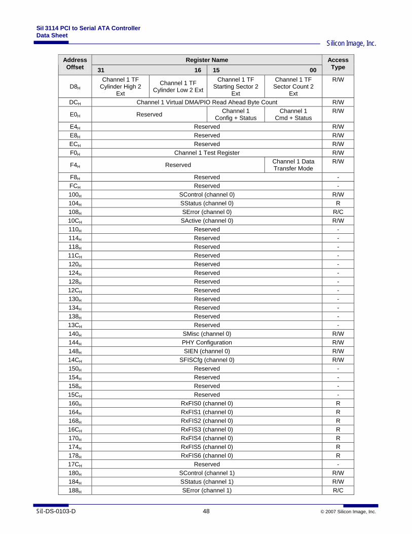
SiI3114 PCI to Serial ATA Controller Data Sheet
Silicon Image, Inc.
SiI-DS-0103-D 48 © 2007 Silicon Image, Inc.
Register Name Address Offset 31 16 15 00
Access Type
D8H Channel 1 TF
Cylinder High 2 Ext
Channel 1 TF Cylinder Low 2 Ext
Channel 1 TF Starting Sector 2
Ext
Channel 1 TF Sector Count 2
Ext
R/W
DCH Channel 1 Virtual DMA/PIO Read Ahead Byte Count R/W
E0H Reserved Channel 1 Config + Status
Channel 1 Cmd + Status
R/W
E4H Reserved R/W E8H Reserved R/W ECH Reserved R/W F0H Channel 1 Test Register R/W
F4H Reserved Channel 1 Data Transfer Mode
R/W
F8H Reserved - FCH Reserved - 100H SControl (channel 0) R/W 104H SStatus (channel 0) R 108H SError (channel 0) R/C 10CH SActive (channel 0) R/W 110H Reserved - 114H Reserved - 118H Reserved - 11CH Reserved - 120H Reserved - 124H Reserved - 128H Reserved - 12CH Reserved - 130H Reserved - 134H Reserved - 138H Reserved - 13CH Reserved - 140H SMisc (channel 0) R/W 144H PHY Configuration R/W 148H SIEN (channel 0) R/W 14CH SFISCfg (channel 0) R/W 150H Reserved - 154H Reserved - 158H Reserved - 15CH Reserved - 160H RxFIS0 (channel 0) R 164H RxFIS1 (channel 0) R 168H RxFIS2 (channel 0) R 16CH RxFIS3 (channel 0) R 170H RxFIS4 (channel 0) R 174H RxFIS5 (channel 0) R 178H RxFIS6 (channel 0) R 17CH Reserved - 180H SControl (channel 1) R/W 184H SStatus (channel 1) R/W 188H SError (channel 1) R/C
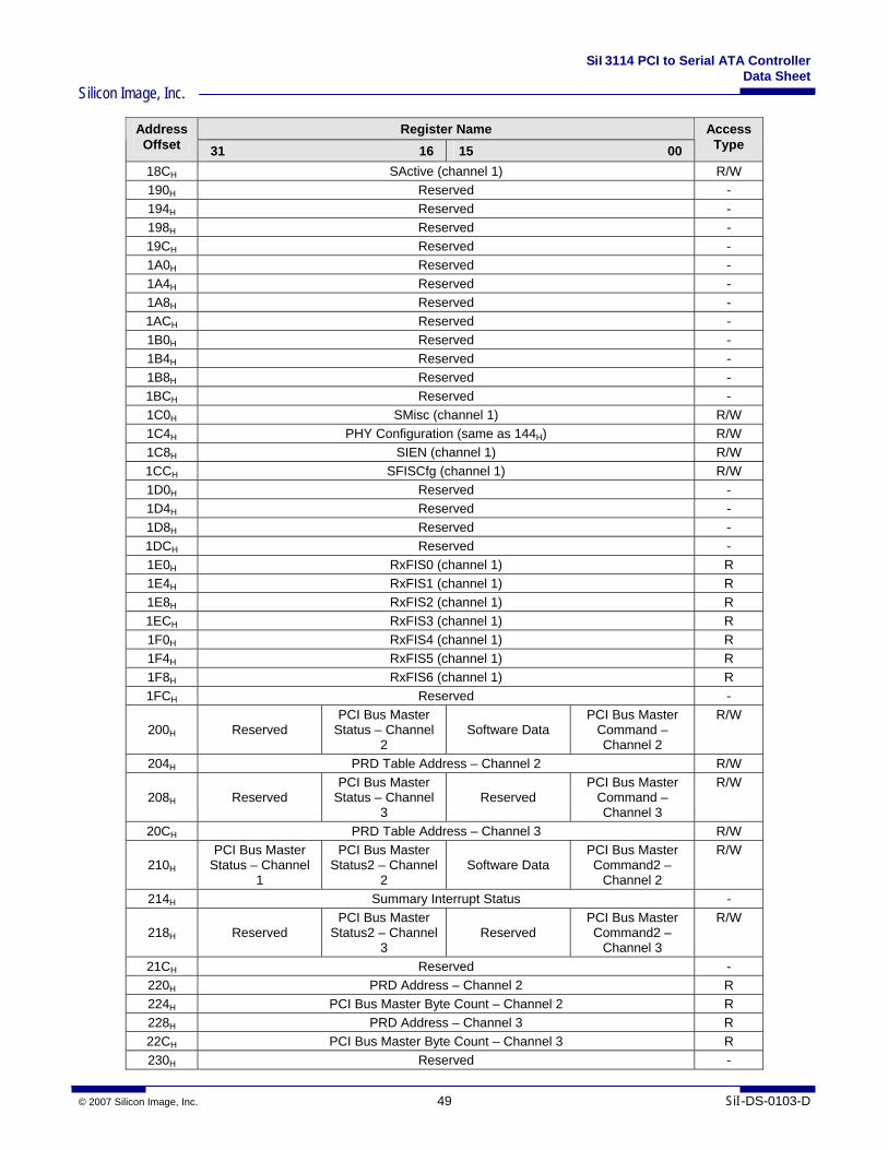
SiI3114 PCI to Serial ATA Controller Data Sheet
Silicon Image, Inc.
© 2007 Silicon Image, Inc. 49 SiI-DS-0103-D
Register Name Address Offset 31 16 15 00
Access Type
18CH SActive (channel 1) R/W 190H Reserved - 194H Reserved - 198H Reserved - 19CH Reserved - 1A0H Reserved - 1A4H Reserved - 1A8H Reserved - 1ACH Reserved - 1B0H Reserved - 1B4H Reserved - 1B8H Reserved - 1BCH Reserved - 1C0H SMisc (channel 1) R/W 1C4H PHY Configuration (same as 144H) R/W 1C8H SIEN (channel 1) R/W 1CCH SFISCfg (channel 1) R/W 1D0H Reserved - 1D4H Reserved - 1D8H Reserved - 1DCH Reserved - 1E0H RxFIS0 (channel 1) R 1E4H RxFIS1 (channel 1) R 1E8H RxFIS2 (channel 1) R 1ECH RxFIS3 (channel 1) R 1F0H RxFIS4 (channel 1) R 1F4H RxFIS5 (channel 1) R 1F8H RxFIS6 (channel 1) R 1FCH Reserved -
200H Reserved PCI Bus Master
Status – Channel 2
Software Data PCI Bus Master
Command – Channel 2
R/W
204H PRD Table Address – Channel 2 R/W
208H Reserved PCI Bus Master
Status – Channel 3
Reserved PCI Bus Master
Command – Channel 3
R/W
20CH PRD Table Address – Channel 3 R/W
210H PCI Bus Master
Status – Channel 1
PCI Bus Master Status2 – Channel
2 Software Data
PCI Bus Master Command2 –
Channel 2
R/W
214H Summary Interrupt Status -
218H Reserved PCI Bus Master
Status2 – Channel 3
Reserved PCI Bus Master Command2 –
Channel 3
R/W
21CH Reserved - 220H PRD Address – Channel 2 R 224H PCI Bus Master Byte Count – Channel 2 R 228H PRD Address – Channel 3 R 22CH PCI Bus Master Byte Count – Channel 3 R 230H Reserved -
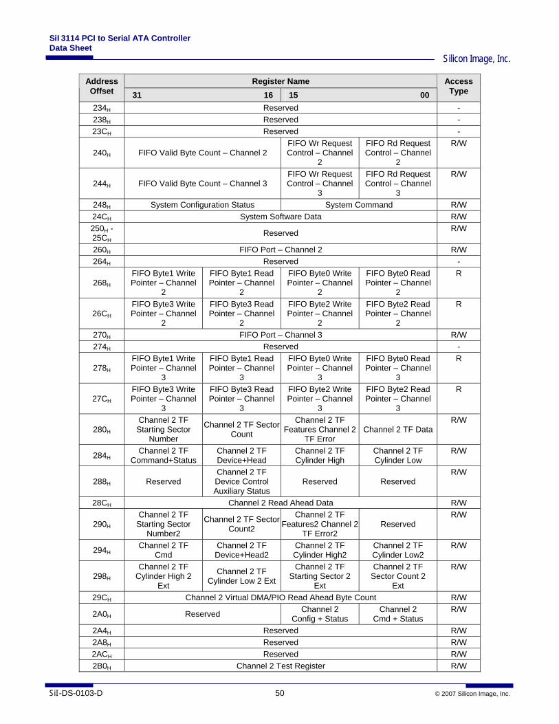
SiI3114 PCI to Serial ATA Controller Data Sheet
Silicon Image, Inc.
SiI-DS-0103-D 50 © 2007 Silicon Image, Inc.
Register Name Address Offset 31 16 15 00
Access Type
234H Reserved - 238H Reserved - 23CH Reserved -
240H FIFO Valid Byte Count – Channel 2 FIFO Wr Request Control – Channel
2
FIFO Rd Request Control – Channel
2
R/W
244H FIFO Valid Byte Count – Channel 3 FIFO Wr Request Control – Channel
3
FIFO Rd Request Control – Channel
3
R/W
248H System Configuration Status System Command R/W 24CH System Software Data R/W 250H -25CH Reserved R/W
260H FIFO Port – Channel 2 R/W 264H Reserved -
268H FIFO Byte1 Write Pointer – Channel
2
FIFO Byte1 Read Pointer – Channel
2
FIFO Byte0 Write Pointer – Channel
2
FIFO Byte0 Read Pointer – Channel
2
R
26CH FIFO Byte3 Write Pointer – Channel
2
FIFO Byte3 Read Pointer – Channel
2
FIFO Byte2 Write Pointer – Channel
2
FIFO Byte2 Read Pointer – Channel
2
R
270H FIFO Port – Channel 3 R/W 274H Reserved -
278H FIFO Byte1 Write Pointer – Channel
3
FIFO Byte1 Read Pointer – Channel
3
FIFO Byte0 Write Pointer – Channel
3
FIFO Byte0 Read Pointer – Channel
3
R
27CH FIFO Byte3 Write Pointer – Channel
3
FIFO Byte3 Read Pointer – Channel
3
FIFO Byte2 Write Pointer – Channel
3
FIFO Byte2 Read Pointer – Channel
3
R
280H Channel 2 TF Starting Sector
Number
Channel 2 TF Sector Count
Channel 2 TF Features Channel 2
TF Error Channel 2 TF Data
R/W
284H Channel 2 TF Command+Status
Channel 2 TF Device+Head
Channel 2 TF Cylinder High
Channel 2 TF Cylinder Low
R/W
288H Reserved Channel 2 TF Device Control Auxiliary Status
Reserved Reserved R/W
28CH Channel 2 Read Ahead Data R/W
290H Channel 2 TF Starting Sector
Number2
Channel 2 TF Sector Count2
Channel 2 TF Features2 Channel 2
TF Error2 Reserved
R/W
294H Channel 2 TF Cmd
Channel 2 TF Device+Head2
Channel 2 TF Cylinder High2
Channel 2 TF Cylinder Low2
R/W
298H Channel 2 TF
Cylinder High 2 Ext
Channel 2 TF Cylinder Low 2 Ext
Channel 2 TF Starting Sector 2
Ext
Channel 2 TF Sector Count 2
Ext
R/W
29CH Channel 2 Virtual DMA/PIO Read Ahead Byte Count R/W
2A0H Reserved Channel 2 Config + Status
Channel 2 Cmd + Status
R/W
2A4H Reserved R/W 2A8H Reserved R/W 2ACH Reserved R/W 2B0H Channel 2 Test Register R/W
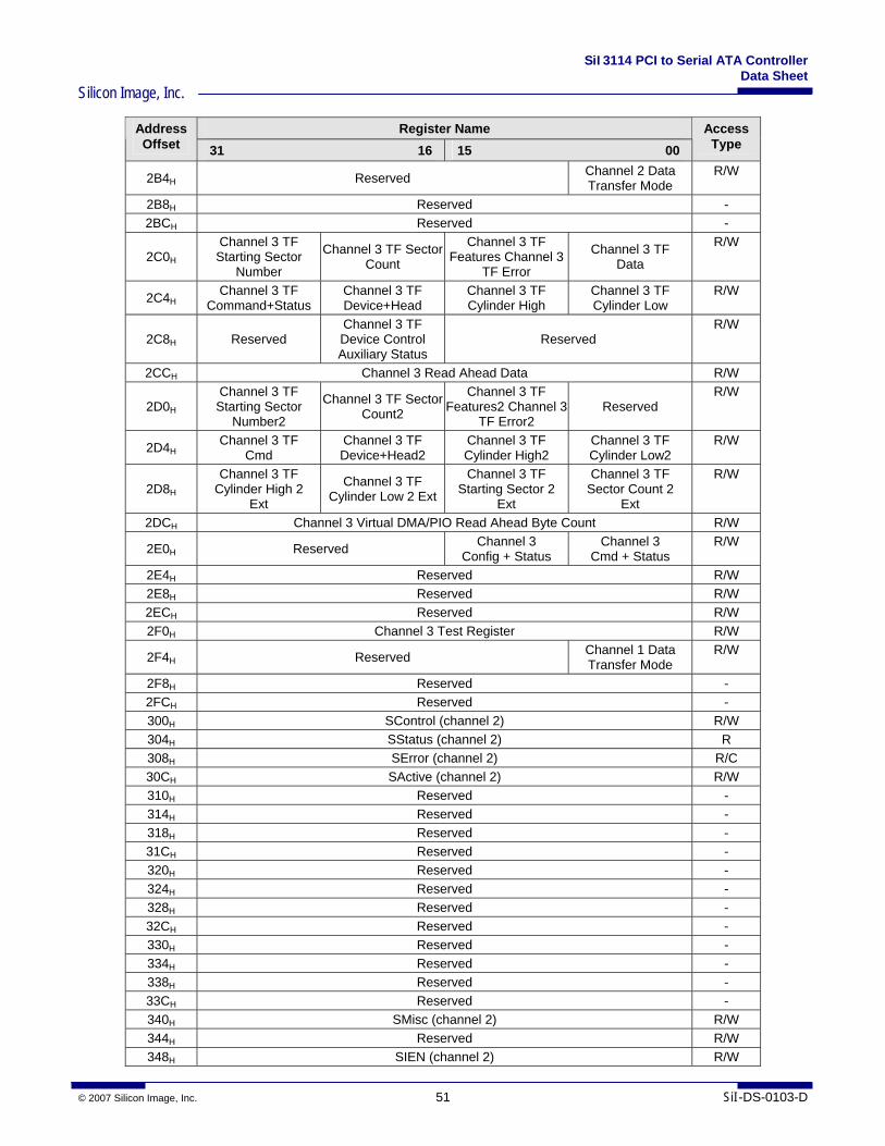
SiI3114 PCI to Serial ATA Controller Data Sheet
Silicon Image, Inc.
© 2007 Silicon Image, Inc. 51 SiI-DS-0103-D
Register Name Address Offset 31 16 15 00
Access Type
2B4H Reserved Channel 2 Data Transfer Mode
R/W
2B8H Reserved - 2BCH Reserved -
2C0H Channel 3 TF Starting Sector
Number
Channel 3 TF Sector Count
Channel 3 TF Features Channel 3
TF Error
Channel 3 TF Data
R/W
2C4H Channel 3 TF Command+Status
Channel 3 TF Device+Head
Channel 3 TF Cylinder High
Channel 3 TF Cylinder Low
R/W
2C8H Reserved Channel 3 TF Device Control Auxiliary Status
Reserved R/W
2CCH Channel 3 Read Ahead Data R/W
2D0H Channel 3 TF Starting Sector
Number2
Channel 3 TF Sector Count2
Channel 3 TF Features2 Channel 3
TF Error2 Reserved
R/W
2D4H Channel 3 TF Cmd
Channel 3 TF Device+Head2
Channel 3 TF Cylinder High2
Channel 3 TF Cylinder Low2
R/W
2D8H Channel 3 TF
Cylinder High 2 Ext
Channel 3 TF Cylinder Low 2 Ext
Channel 3 TF Starting Sector 2
Ext
Channel 3 TF Sector Count 2
Ext
R/W
2DCH Channel 3 Virtual DMA/PIO Read Ahead Byte Count R/W
2E0H Reserved Channel 3 Config + Status
Channel 3 Cmd + Status
R/W
2E4H Reserved R/W 2E8H Reserved R/W 2ECH Reserved R/W 2F0H Channel 3 Test Register R/W
2F4H Reserved Channel 1 Data Transfer Mode
R/W
2F8H Reserved - 2FCH Reserved - 300H SControl (channel 2) R/W 304H SStatus (channel 2) R 308H SError (channel 2) R/C 30CH SActive (channel 2) R/W 310H Reserved - 314H Reserved - 318H Reserved - 31CH Reserved - 320H Reserved - 324H Reserved - 328H Reserved - 32CH Reserved - 330H Reserved - 334H Reserved - 338H Reserved - 33CH Reserved - 340H SMisc (channel 2) R/W 344H Reserved R/W 348H SIEN (channel 2) R/W
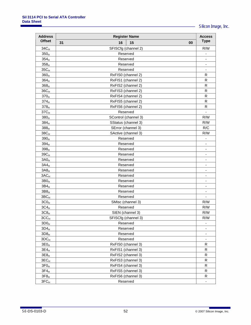
SiI3114 PCI to Serial ATA Controller Data Sheet
Silicon Image, Inc.
SiI-DS-0103-D 52 © 2007 Silicon Image, Inc.
Register Name Address Offset 31 16 15 00
Access Type
34CH SFISCfg (channel 2) R/W 350H Reserved - 354H Reserved - 358H Reserved - 35CH Reserved - 360H RxFIS0 (channel 2) R 364H RxFIS1 (channel 2) R 368H RxFIS2 (channel 2) R 36CH RxFIS3 (channel 2) R 370H RxFIS4 (channel 2) R 374H RxFIS5 (channel 2) R 378H RxFIS6 (channel 2) R 37CH Reserved - 380H SControl (channel 3) R/W 384H SStatus (channel 3) R/W 388H SError (channel 3) R/C 38CH SActive (channel 3) R/W 390H Reserved - 394H Reserved - 398H Reserved - 39CH Reserved - 3A0H Reserved - 3A4H Reserved - 3A8H Reserved - 3ACH Reserved - 3B0H Reserved - 3B4H Reserved - 3B8H Reserved - 3BCH Reserved - 3C0H SMisc (channel 3) R/W 3C4H Reserved R/W 3C8H SIEN (channel 3) R/W 3CCH SFISCfg (channel 3) R/W 3D0H Reserved - 3D4H Reserved - 3D8H Reserved - 3DCH Reserved - 3E0H RxFIS0 (channel 3) R 3E4H RxFIS1 (channel 3) R 3E8H RxFIS2 (channel 3) R 3ECH RxFIS3 (channel 3) R 3F0H RxFIS4 (channel 3) R 3F4H RxFIS5 (channel 3) R 3F8H RxFIS6 (channel 3) R 3FCH Reserved -
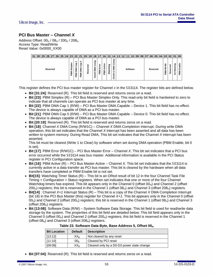
SiI3114 PCI to Serial ATA Controller Data Sheet
Silicon Image, Inc.
© 2007 Silicon Image, Inc. 53 SiI-DS-0103-D
PCI Bus Master – Channel X Address Offset: 00H / 08H / 200H / 208H Access Type: Read/Write Reset Value: 0x0000_XX00
31 30 29 28 27 26 25 24 23 22 21 20 19 18 17 16 15 14 13 12 11 10 09 08 07 06 05 04 03 02 01 00
Reserved PB
M S
impl
ex
PBM
DM
A C
ap 1
PBM
DM
A C
ap 0
Res
erve
d
Chn
lX D
MA
Com
p
PBM
Err
or
PBM
Act
ive
Wat
chdo
g
Chn
lX+1
DM
A C
omp
Software Reserved
PBM
Rd-
Wr
Res
erve
d
Int S
teer
ing
PBM
Ena
ble
This register defines the PCI bus master register for Channel X in the SiI3114. The register bits are defined below.
• Bit [31:24]: Reserved (R). This bit field is reserved and returns zeros on a read. • Bit [23]: PBM Simplex (R) – PCI Bus Master Simplex Only. This read-only bit field is hardwired to zero to
indicate that all channels can operate as PCI bus master at any time. • Bit [22]: PBM DMA Cap 1 (R/W) – PCI Bus Master DMA Capable – Device 1. This bit field has no effect.
The device is always capable of DMA as a PCI bus master. • Bit [21]: PBM DMA Cap 0 (R/W) – PCI Bus Master DMA Capable – Device 0. This bit field has no effect.
The device is always capable of DMA as a PCI bus master. • Bit [20:19]: Reserved (R). This bit field is reserved and returns zeros on a read. • Bit [18]: Channel X DMA Comp (R/W1C) – Channel X DMA Completion Interrupt. During write DMA
operation, this bit set indicates that the Channel X interrupt has been asserted and all data has been written to system memory. During Read DMA, This bit set indicates that the Channel X interrupt has been asserted. This bit must be cleared (Write 1 to Clear) by software when set during DMA operation (PBM Enable, bit 0 is set).
• Bit [17]: PBM Error (R/W1C) – PCI Bus Master Error – Channel X. This bit set indicates that a PCI bus error occurred while the SiI3114 was bus master. Additional information is available in the PCI Status register in PCI Configuration space.
• Bit [16]: PBM Active (R) – PCI Bus Master Active – Channel X. This bit set indicates that the SiI3114 is currently active in a data transfer as PCI bus master. This bit is cleared by the hardware when all data transfers have completed or PBM Enable bit is not set.
• Bit[15]: Watchdog Timer Status (R) – This bit is an ORed result of bit 12 in the four Channel Task File Timing + Configuration + Status registers. When set indicates that one or more of the four Channel Watchdog timers has expired. This bit appears only in the Channel 0 (offset 00H) and Channel 2 (offset 200H) registers; this bit is reserved in the Channel 1 (offset 08H) and Channel 3 (offset 208H) registers.
• Bit[14] : Channel X+1 Interrupt Status (R) – This bit is a copy of the Channel X DMA Completion Interrupt (bit 18) in the PCI Bus Master (this) register for Channel X+1. This bit appears only in the Channel 0 (offset 00H) and Channel 2 (offset 200H) registers; this bit is reserved in the Channel 1 (offset 08H) and Channel 3 (offset 208H) registers.
• Bit [13:08]: Software Data (R/W) – System Software Data Storage. This bit field is used for read/write data storage by the system. The properties of this bit field are detailed below. This bit field appears only in the Channel 0 (offset 00H) and Channel 2 (offset 200H) registers; this bit field is reserved in the Channel 1 (offset 08H) and Channel 3 (offset 208H) registers.
Table 23. Software Data Byte, Base Address 5, Offset 00H Bit Location Default Description [13:12] XXB Not cleared by any reset [11:10] 00B Cleared by PCI reset [09:08] XXB Cleared only by a D0-D3 power state change
• Bit [07:04]: Reserved (R). This bit field is reserved and returns zeros on a read.
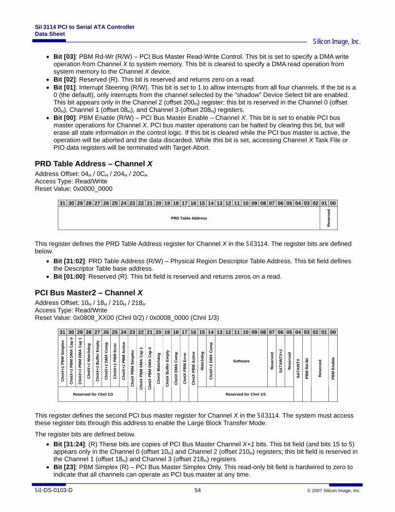
SiI3114 PCI to Serial ATA Controller Data Sheet
Silicon Image, Inc.
SiI-DS-0103-D 54 © 2007 Silicon Image, Inc.
• Bit [03]: PBM Rd-Wr (R/W) – PCI Bus Master Read-Write Control. This bit is set to specify a DMA write operation from Channel X to system memory. This bit is cleared to specify a DMA read operation from system memory to the Channel X device.
• Bit [02]: Reserved (R). This bit is reserved and returns zero on a read. • Bit [01]: Interrupt Steering (R/W). This bit is set to 1 to allow interrupts from all four channels. If the bit is a
0 (the default), only interrupts from the channel selected by the “shadow” Device Select bit are enabled. This bit appears only in the Channel 2 (offset 200H) register; this bit is reserved in the Channel 0 (offset 00H), Channel 1 (offset 08H), and Channel 3 (offset 208H) registers.
• Bit [00]: PBM Enable (R/W) – PCI Bus Master Enable – Channel X. This bit is set to enable PCI bus master operations for Channel X. PCI bus master operations can be halted by clearing this bit, but will erase all state information in the control logic. If this bit is cleared while the PCI bus master is active, the operation will be aborted and the data discarded. While this bit is set, accessing Channel X Task File or PIO data registers will be terminated with Target-Abort.
PRD Table Address – Channel X Address Offset: 04H / 0CH / 204H / 20CH Access Type: Read/Write Reset Value: 0x0000_0000
31 30 29 28 27 26 25 24 23 22 21 20 19 18 17 16 15 14 13 12 11 10 09 08 07 06 05 04 03 02 01 00
PRD Table Address
Res
erve
d
This register defines the PRD Table Address register for Channel X in the SiI3114. The register bits are defined below.
• Bit [31:02]: PRD Table Address (R/W) – Physical Region Descriptor Table Address. This bit field defines the Descriptor Table base address.
• Bit [01:00]: Reserved (R). This bit field is reserved and returns zeros on a read.
PCI Bus Master2 – Channel X Address Offset: 10H / 18H / 210H / 218H Access Type: Read/Write Reset Value: 0x0808_XX00 (Chnl 0/2) / 0x0008_0000 (Chnl 1/3)
31 30 29 28 27 26 25 24 23 22 21 20 19 18 17 16 15 14 13 12 11 10 09 08 07 06 05 04 03 02 01 00
Chn
lX+1
PB
M S
impl
ex
Chn
lX+1
PB
M D
MA
Cap
0
Chn
lX+1
PB
M D
MA
Cap
1
Chn
lX+1
Wat
chdo
g
Chn
lX+1
Buf
fer E
mpt
y
Chn
lX+1
DM
A C
omp
Chn
lX+1
PB
M E
rror
Chn
lX+1
PB
M A
ctiv
e
Wat
chdo
g
Chn
lX+1
DM
A C
omp
Software
Res
erve
d
SATA
INTX
+1
Res
erve
d
Reserved for Chnl 1/3
Chn
lX P
BM
Sim
plex
Chn
lX P
BM
DM
A C
ap 1
Chn
lX P
BM
DM
A C
ap 0
Chn
lX W
atch
dog
Chn
lX B
uffe
r Em
pty
Chn
lX D
MA
Com
p
Chn
lX P
BM
Err
or
Chn
lX P
BM
Act
ive
Reserved for Chnl 1/3
SATA
INTX
PBM
Rd-
Wr
Res
erve
d
PBM
Ena
ble
This register defines the second PCI bus master register for Channel X in the SiI3114. The system must access these register bits through this address to enable the Large Block Transfer Mode.
The register bits are defined below. • Bit [31:24]: (R) These bits are copies of PCI Bus Master Channel X+1 bits. This bit field (and bits 15 to 5)
appears only in the Channel 0 (offset 10H) and Channel 2 (offset 210H) registers; this bit field is reserved in the Channel 1 (offset 18H) and Channel 3 (offset 218H) registers.
• Bit [23]: PBM Simplex (R) – PCI Bus Master Simplex Only. This read-only bit field is hardwired to zero to indicate that all channels can operate as PCI bus master at any time.
SiI3114 PCI to Serial ATA Controller Data Sheet
Silicon Image, Inc.
© 2007 Silicon Image, Inc. 55 SiI-DS-0103-D
• Bit [22]: PBM DMA Cap 1 (R/W) – PCI Bus Master DMA Capable – Device 1. This bit field has no effect. The device is always capable of DMA as a PCI bus master.
• Bit [21]: PBM DMA Cap 0 (R/W) – PCI Bus Master DMA Capable – Device 0. This bit field has no effect. The device is always capable of DMA as a PCI bus master.
• Bit [20]: Watchdog (R): This bit is a copy of bit 12 in Channel X Task File Configuration + Status register. • Bit [19]: Channel X Buffer empty (R). This bit set indicates the Channel X FIFO is empty. • Bit [18]: Channel X DMA Comp (R/W1C) – Channel X DMA Completion Interrupt. During write DMA
operation, this bit set indicates that the Channel X interrupt has been asserted and all data has been written to system memory. During Read DMA, this bit set indicates that the Channel X interrupt has been asserted. This bit must be cleared by software (Write 1 to Clear) when set during DMA operation (PBM Enable, bit 0 is set).
• Bit [17]: PBM Error (R/W1C) – PCI Bus Master Error – Channel 0. This bit set indicates that a PCI bus error occurred while the SiI3114 was bus master. Additional information is available in the PCI Status register in PCI Configuration space.
• Bit [16]: PBM Active (R) – PCI Bus Master Active – Channel 0. This bit set indicates that the SiI3114 is currently active in a data transfer as PCI bus master. This bit is cleared by the hardware when all data transfers have completed or PBM Enable bit is not set.
• Bit[15] : Watchdog Timer Status ( R ) – This bit is an ORed result of bit 12 in the four Channel Task File Timing + Configuration + Status registers. When set indicates that one or more of the four Channel Watchdog timers has expired.
• Bit[14] : Channel X+1 DMA Completion Interrupt Status ( R ) – This bit is a copy of the Channel X DMA Completion Interrupt (bit 18) in the PCI Bus Master register for Channel X+1.
• Bit [13:08]: Software Data (R/W) – System Software Data Storage. This bit field is used for read/write data storage by the system. The properties of this bit field are detailed below.
Table 24. Software Data Byte, Base Address 5, Offset 10H Bit Location Default Description [13:12] XXB Not cleared by any reset [11:10] 00B Cleared by PCI reset [09:08] XXB Cleared only by a D0-D3 power state change
• Bit [07]: Reserved (R). This bit is reserved and returns zeros on a read. • Bit [06]: SATAINTX+1 – This bit is the logical OR of all Serial ATA interrupt sources for channel X+1. • Bit [05]: Reserved (R). This bit is reserved and returns zeros on a read. • Bit [04]: SATAINTX – This bit is the logical OR of all Serial ATA interrupt sources for channel X. • Bit [03]: PBM Rd-Wr (R/W) – PCI Bus Master Read-Write Control. This bit is set to specify a DMA write
operation from Channel X to system memory. This bit is cleared to specify a DMA read operation from system memory to the Channel X device.
• Bit [02:01]: Reserved (R). This bit field is reserved and returns zeros on a read. • Bit [00]: PBM Enable (R/W) – PCI Bus Master Enable – Channel X. This bit is set to enable PCI bus
master operations for Channel X. PCI bus master operations can be halted by clearing this bit, but will erase all state information in the control logic. If this bit is cleared while the PCI bus master is active, the operation will be aborted and the data discarded. While this bit is set, accessing Channel X Task File or PIO data registers will be terminated with Target-Abort.
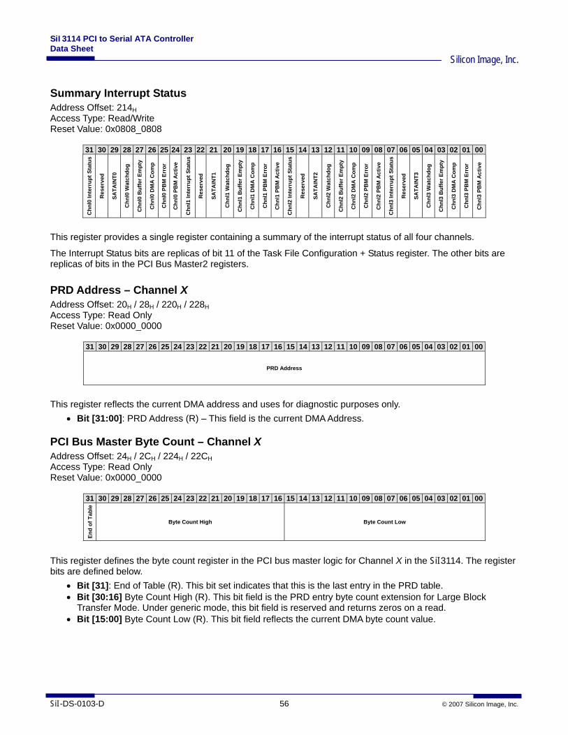
SiI3114 PCI to Serial ATA Controller Data Sheet
Silicon Image, Inc.
SiI-DS-0103-D 56 © 2007 Silicon Image, Inc.
Summary Interrupt Status Address Offset: 214H Access Type: Read/Write Reset Value: 0x0808_0808
31 30 29 28 27 26 25 24 23 22 21 20 19 18 17 16 15 14 13 12 11 10 09 08 07 06 05 04 03 02 01 00
Chn
l0 In
terr
upt S
tatu
s
Res
erve
d
SATA
INT0
Chn
l0 W
atch
dog
Chn
l0 B
uffe
r Em
pty
Chn
l0 D
MA
Com
p
Chn
l0 P
BM
Err
or
Chn
l0 P
BM
Act
ive
Chn
l1 In
terr
upt S
tatu
s
Res
erve
d
SATA
INT1
Chn
l1 W
atch
dog
Chn
l1 B
uffe
r Em
pty
Chn
l1 D
MA
Com
p
Chn
l1 P
BM
Err
or
Chn
l1 P
BM
Act
ive
Chn
l2 In
terr
upt S
tatu
s
Res
erve
d
SATA
INT2
Chn
l2 W
atch
dog
Chn
l2 B
uffe
r Em
pty
Chn
l2 D
MA
Com
p
Chn
l2 P
BM
Err
or
Chn
l2 P
BM
Act
ive
Chn
l3 In
terr
upt S
tatu
s
Res
erve
d
SATA
INT3
Chn
l3 W
atch
dog
Chn
l3 B
uffe
r Em
pty
Chn
l3 D
MA
Com
p
Chn
l3 P
BM
Err
or
Chn
l3 P
BM
Act
ive
This register provides a single register containing a summary of the interrupt status of all four channels.
The Interrupt Status bits are replicas of bit 11 of the Task File Configuration + Status register. The other bits are replicas of bits in the PCI Bus Master2 registers.
PRD Address – Channel X Address Offset: 20H / 28H / 220H / 228H Access Type: Read Only Reset Value: 0x0000_0000
31 30 29 28 27 26 25 24 23 22 21 20 19 18 17 16 15 14 13 12 11 10 09 08 07 06 05 04 03 02 01 00
PRD Address
This register reflects the current DMA address and uses for diagnostic purposes only.
• Bit [31:00]: PRD Address (R) – This field is the current DMA Address.
PCI Bus Master Byte Count – Channel X Address Offset: 24H / 2CH / 224H / 22CH Access Type: Read Only Reset Value: 0x0000_0000
31 30 29 28 27 26 25 24 23 22 21 20 19 18 17 16 15 14 13 12 11 10 09 08 07 06 05 04 03 02 01 00
End
of T
able
Byte Count High Byte Count Low
This register defines the byte count register in the PCI bus master logic for Channel X in the SiI3114. The register bits are defined below.
• Bit [31]: End of Table (R). This bit set indicates that this is the last entry in the PRD table. • Bit [30:16] Byte Count High (R). This bit field is the PRD entry byte count extension for Large Block
Transfer Mode. Under generic mode, this bit field is reserved and returns zeros on a read. • Bit [15:00] Byte Count Low (R). This bit field reflects the current DMA byte count value.
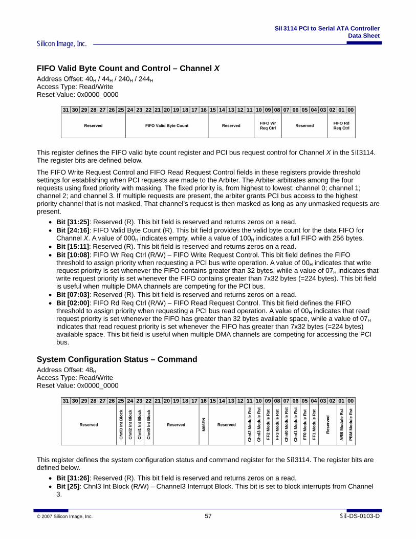
SiI3114 PCI to Serial ATA Controller Data Sheet
Silicon Image, Inc.
© 2007 Silicon Image, Inc. 57 SiI-DS-0103-D
FIFO Valid Byte Count and Control – Channel X Address Offset: 40H / 44H / 240H / 244H Access Type: Read/Write Reset Value: 0x0000_0000
31 30 29 28 27 26 25 24 23 22 21 20 19 18 17 16 15 14 13 12 11 10 09 08 07 06 05 04 03 02 01 00
Reserved FIFO Valid Byte Count Reserved FIFO Wr Req Ctrl Reserved FIFO Rd
Req Ctrl
This register defines the FIFO valid byte count register and PCI bus request control for Channel X in the SiI3114. The register bits are defined below.
The FIFO Write Request Control and FIFO Read Request Control fields in these registers provide threshold settings for establishing when PCI requests are made to the Arbiter. The Arbiter arbitrates among the four requests using fixed priority with masking. The fixed priority is, from highest to lowest: channel 0; channel 1; channel 2; and channel 3. If multiple requests are present, the arbiter grants PCI bus access to the highest priority channel that is not masked. That channel’s request is then masked as long as any unmasked requests are present.
• Bit [31:25]: Reserved (R). This bit field is reserved and returns zeros on a read. • Bit [24:16]: FIFO Valid Byte Count (R). This bit field provides the valid byte count for the data FIFO for
Channel X. A value of 000H indicates empty, while a value of 100H indicates a full FIFO with 256 bytes. • Bit [15:11]: Reserved (R). This bit field is reserved and returns zeros on a read. • Bit [10:08]: FIFO Wr Req Ctrl (R/W) – FIFO Write Request Control. This bit field defines the FIFO
threshold to assign priority when requesting a PCI bus write operation. A value of 00H indicates that write request priority is set whenever the FIFO contains greater than 32 bytes, while a value of 07H indicates that write request priority is set whenever the FIFO contains greater than 7x32 bytes (=224 bytes). This bit field is useful when multiple DMA channels are competing for the PCI bus.
• Bit [07:03]: Reserved (R). This bit field is reserved and returns zeros on a read. • Bit [02:00]: FIFO Rd Req Ctrl (R/W) – FIFO Read Request Control. This bit field defines the FIFO
threshold to assign priority when requesting a PCI bus read operation. A value of 00H indicates that read request priority is set whenever the FIFO has greater than 32 bytes available space, while a value of 07H indicates that read request priority is set whenever the FIFO has greater than 7x32 bytes (=224 bytes) available space. This bit field is useful when multiple DMA channels are competing for accessing the PCI bus.
System Configuration Status – Command Address Offset: 48H Access Type: Read/Write Reset Value: 0x0000_0000
31 30 29 28 27 26 25 24 23 22 21 20 19 18 17 16 15 14 13 12 11 10 09 08 07 06 05 04 03 02 01 00
Reserved
Chn
l3 In
t Blo
ck
Chn
l2 In
t Blo
ck
Chn
l1 In
t Blo
ck
Chn
l0 In
t Blo
ck
Reserved
M66
EN
Reserved
Chn
l2 M
odul
e R
st
Chn
l3 M
odul
e R
st
FF2
Mod
ule
Rst
FF3
Mod
ule
Rst
Chn
l0 M
odul
e R
st
Chn
l1 M
odul
e R
st
FF0
Mod
ule
Rst
FF1
Mod
ule
Rst
Res
erve
d
AR
B M
odul
e R
st
PBM
Mod
ule
Rst
This register defines the system configuration status and command register for the SiI3114. The register bits are defined below.
• Bit [31:26]: Reserved (R). This bit field is reserved and returns zeros on a read. • Bit [25]: Chnl3 Int Block (R/W) – Channel3 Interrupt Block. This bit is set to block interrupts from Channel
3.
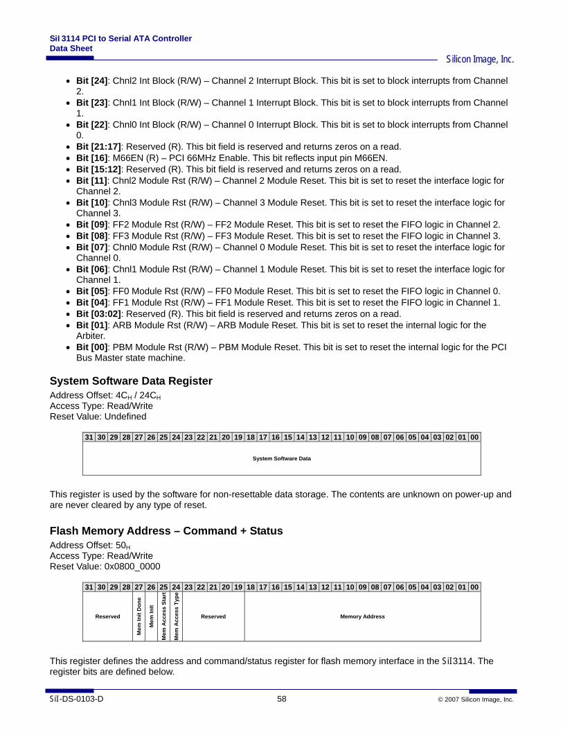
SiI3114 PCI to Serial ATA Controller Data Sheet
Silicon Image, Inc.
SiI-DS-0103-D 58 © 2007 Silicon Image, Inc.
• Bit [24]: Chnl2 Int Block (R/W) – Channel 2 Interrupt Block. This bit is set to block interrupts from Channel 2.
• Bit [23]: Chnl1 Int Block (R/W) – Channel 1 Interrupt Block. This bit is set to block interrupts from Channel 1.
• Bit [22]: Chnl0 Int Block (R/W) – Channel 0 Interrupt Block. This bit is set to block interrupts from Channel 0.
• Bit [21:17]: Reserved (R). This bit field is reserved and returns zeros on a read. • Bit [16]: M66EN (R) – PCI 66MHz Enable. This bit reflects input pin M66EN. • Bit [15:12]: Reserved (R). This bit field is reserved and returns zeros on a read. • Bit [11]: Chnl2 Module Rst (R/W) – Channel 2 Module Reset. This bit is set to reset the interface logic for
Channel 2. • Bit [10]: Chnl3 Module Rst (R/W) – Channel 3 Module Reset. This bit is set to reset the interface logic for
Channel 3. • Bit [09]: FF2 Module Rst (R/W) – FF2 Module Reset. This bit is set to reset the FIFO logic in Channel 2. • Bit [08]: FF3 Module Rst (R/W) – FF3 Module Reset. This bit is set to reset the FIFO logic in Channel 3. • Bit [07]: Chnl0 Module Rst (R/W) – Channel 0 Module Reset. This bit is set to reset the interface logic for
Channel 0. • Bit [06]: Chnl1 Module Rst (R/W) – Channel 1 Module Reset. This bit is set to reset the interface logic for
Channel 1. • Bit [05]: FF0 Module Rst (R/W) – FF0 Module Reset. This bit is set to reset the FIFO logic in Channel 0. • Bit [04]: FF1 Module Rst (R/W) – FF1 Module Reset. This bit is set to reset the FIFO logic in Channel 1. • Bit [03:02]: Reserved (R). This bit field is reserved and returns zeros on a read. • Bit [01]: ARB Module Rst (R/W) – ARB Module Reset. This bit is set to reset the internal logic for the
Arbiter. • Bit [00]: PBM Module Rst (R/W) – PBM Module Reset. This bit is set to reset the internal logic for the PCI
Bus Master state machine.
System Software Data Register Address Offset: 4CH / 24CH Access Type: Read/Write Reset Value: Undefined
31 30 29 28 27 26 25 24 23 22 21 20 19 18 17 16 15 14 13 12 11 10 09 08 07 06 05 04 03 02 01 00
System Software Data
This register is used by the software for non-resettable data storage. The contents are unknown on power-up and are never cleared by any type of reset.
Flash Memory Address – Command + Status Address Offset: 50H Access Type: Read/Write Reset Value: 0x0800_0000
31 30 29 28 27 26 25 24 23 22 21 20 19 18 17 16 15 14 13 12 11 10 09 08 07 06 05 04 03 02 01 00
Reserved
Mem
Init
Don
e
Mem
Init
Mem
Acc
ess
Star
t
Mem
Acc
ess
Type
Reserved Memory Address
This register defines the address and command/status register for flash memory interface in the SiI3114. The register bits are defined below.
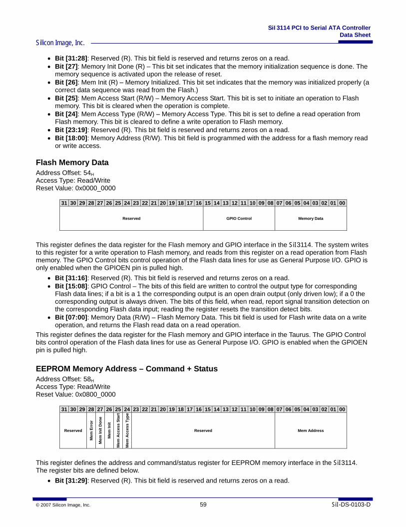
SiI3114 PCI to Serial ATA Controller Data Sheet
Silicon Image, Inc.
© 2007 Silicon Image, Inc. 59 SiI-DS-0103-D
• Bit [31:28]: Reserved (R). This bit field is reserved and returns zeros on a read. • Bit [27]: Memory Init Done (R) – This bit set indicates that the memory initialization sequence is done. The
memory sequence is activated upon the release of reset. • Bit [26]: Mem Init (R) – Memory Initialized. This bit set indicates that the memory was initialized properly (a
correct data sequence was read from the Flash.) • Bit [25]: Mem Access Start (R/W) – Memory Access Start. This bit is set to initiate an operation to Flash
memory. This bit is cleared when the operation is complete. • Bit [24]: Mem Access Type (R/W) – Memory Access Type. This bit is set to define a read operation from
Flash memory. This bit is cleared to define a write operation to Flash memory. • Bit [23:19]: Reserved (R). This bit field is reserved and returns zeros on a read. • Bit [18:00]: Memory Address (R/W). This bit field is programmed with the address for a flash memory read
or write access.
Flash Memory Data Address Offset: 54H Access Type: Read/Write Reset Value: 0x0000_0000
31 30 29 28 27 26 25 24 23 22 21 20 19 18 17 16 15 14 13 12 11 10 09 08 07 06 05 04 03 02 01 00
Reserved GPIO Control Memory Data
This register defines the data register for the Flash memory and GPIO interface in the SiI3114. The system writes to this register for a write operation to Flash memory, and reads from this register on a read operation from Flash memory. The GPIO Control bits control operation of the Flash data lines for use as General Purpose I/O. GPIO is only enabled when the GPIOEN pin is pulled high.
• Bit [31:16]: Reserved (R). This bit field is reserved and returns zeros on a read. • Bit [15:08]: GPIO Control – The bits of this field are written to control the output type for corresponding
Flash data lines; if a bit is a 1 the corresponding output is an open drain output (only driven low); if a 0 the corresponding output is always driven. The bits of this field, when read, report signal transition detection on the corresponding Flash data input; reading the register resets the transition detect bits.
• Bit [07:00]: Memory Data (R/W) – Flash Memory Data. This bit field is used for Flash write data on a write operation, and returns the Flash read data on a read operation.
This register defines the data register for the Flash memory and GPIO interface in the Taurus. The GPIO Control bits control operation of the Flash data lines for use as General Purpose I/O. GPIO is enabled when the GPIOEN pin is pulled high.
EEPROM Memory Address – Command + Status Address Offset: 58H Access Type: Read/Write Reset Value: 0x0800_0000
31 30 29 28 27 26 25 24 23 22 21 20 19 18 17 16 15 14 13 12 11 10 09 08 07 06 05 04 03 02 01 00
Reserved
Mem
Err
or
Mem
Init
Don
e
Mem
Init
Mem
Acc
ess
Star
t
Mem
Acc
ess
Type
Reserved Mem Address
This register defines the address and command/status register for EEPROM memory interface in the SiI3114. The register bits are defined below.
• Bit [31:29]: Reserved (R). This bit field is reserved and returns zeros on a read.
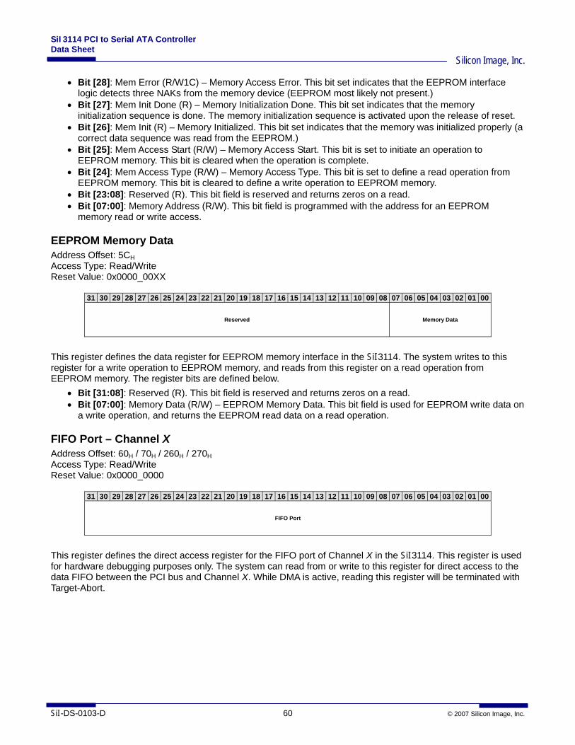
SiI3114 PCI to Serial ATA Controller Data Sheet
Silicon Image, Inc.
SiI-DS-0103-D 60 © 2007 Silicon Image, Inc.
• Bit [28]: Mem Error (R/W1C) – Memory Access Error. This bit set indicates that the EEPROM interface logic detects three NAKs from the memory device (EEPROM most likely not present.)
• Bit [27]: Mem Init Done (R) – Memory Initialization Done. This bit set indicates that the memory initialization sequence is done. The memory initialization sequence is activated upon the release of reset.
• Bit [26]: Mem Init (R) – Memory Initialized. This bit set indicates that the memory was initialized properly (a correct data sequence was read from the EEPROM.)
• Bit [25]: Mem Access Start (R/W) – Memory Access Start. This bit is set to initiate an operation to EEPROM memory. This bit is cleared when the operation is complete.
• Bit [24]: Mem Access Type (R/W) – Memory Access Type. This bit is set to define a read operation from EEPROM memory. This bit is cleared to define a write operation to EEPROM memory.
• Bit [23:08]: Reserved (R). This bit field is reserved and returns zeros on a read. • Bit [07:00]: Memory Address (R/W). This bit field is programmed with the address for an EEPROM
memory read or write access.
EEPROM Memory Data Address Offset: 5CH Access Type: Read/Write Reset Value: 0x0000_00XX
31 30 29 28 27 26 25 24 23 22 21 20 19 18 17 16 15 14 13 12 11 10 09 08 07 06 05 04 03 02 01 00
Reserved Memory Data
This register defines the data register for EEPROM memory interface in the SiI3114. The system writes to this register for a write operation to EEPROM memory, and reads from this register on a read operation from EEPROM memory. The register bits are defined below.
• Bit [31:08]: Reserved (R). This bit field is reserved and returns zeros on a read. • Bit [07:00]: Memory Data (R/W) – EEPROM Memory Data. This bit field is used for EEPROM write data on
a write operation, and returns the EEPROM read data on a read operation.
FIFO Port – Channel X Address Offset: 60H / 70H / 260H / 270H Access Type: Read/Write Reset Value: 0x0000_0000
31 30 29 28 27 26 25 24 23 22 21 20 19 18 17 16 15 14 13 12 11 10 09 08 07 06 05 04 03 02 01 00
FIFO Port
This register defines the direct access register for the FIFO port of Channel X in the SiI3114. This register is used for hardware debugging purposes only. The system can read from or write to this register for direct access to the data FIFO between the PCI bus and Channel X. While DMA is active, reading this register will be terminated with Target-Abort.
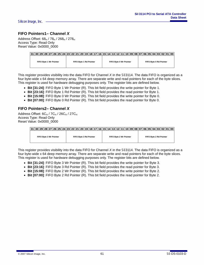
SiI3114 PCI to Serial ATA Controller Data Sheet
Silicon Image, Inc.
© 2007 Silicon Image, Inc. 61 SiI-DS-0103-D
FIFO Pointers1– Channel X Address Offset: 68H / 78H / 268H / 278H Access Type: Read Only Reset Value: 0x0000_0000
31 30 29 28 27 26 25 24 23 22 21 20 19 18 17 16 15 14 13 12 11 10 09 08 07 06 05 04 03 02 01 00
FIFO Byte 1 Wr Pointer FIFO Byte 1 Rd Pointer FIFO Byte 0 Wr Pointer FIFO Byte 0 Rd Pointer
This register provides visibility into the data FIFO for Channel X in the SiI3114. The data FIFO is organized as a four byte-wide x 64 deep memory array. There are separate write and read pointers for each of the byte slices. This register is used for hardware debugging purposes only. The register bits are defined below.
• Bit [31:24]: FIFO Byte 1 Wr Pointer (R). This bit field provides the write pointer for Byte 1. • Bit [23:16]: FIFO Byte 1 Rd Pointer (R). This bit field provides the read pointer for Byte 1. • Bit [15:08]: FIFO Byte 0 Wr Pointer (R). This bit field provides the write pointer for Byte 0. • Bit [07:00]: FIFO Byte 0 Rd Pointer (R). This bit field provides the read pointer for Byte 0.
FIFO Pointers2– Channel X Address Offset: 6CH / 7CH / 26CH / 27CH Access Type: Read Only Reset Value: 0x0000_0000
31 30 29 28 27 26 25 24 23 22 21 20 19 18 17 16 15 14 13 12 11 10 09 08 07 06 05 04 03 02 01 00
FIFO Byte 3 Wr Pointer FIFO Byte 3 Rd Pointer FIFO Byte 2 Wr Pointer FIFO Byte 2 Rd Pointer
This register provides visibility into the data FIFO for Channel X in the SiI3114. The data FIFO is organized as a four byte-wide x 64 deep memory array. There are separate write and read pointers for each of the byte slices. This register is used for hardware debugging purposes only. The register bits are defined below.
• Bit [31:24]: FIFO Byte 3 Wr Pointer (R). This bit field provides the write pointer for Byte 3. • Bit [23:16]: FIFO Byte 3 Rd Pointer (R). This bit field provides the read pointer for Byte 3. • Bit [15:08]: FIFO Byte 2 Wr Pointer (R). This bit field provides the write pointer for Byte 2. • Bit [07:00]: FIFO Byte 2 Rd Pointer (R). This bit field provides the read pointer for Byte 2.
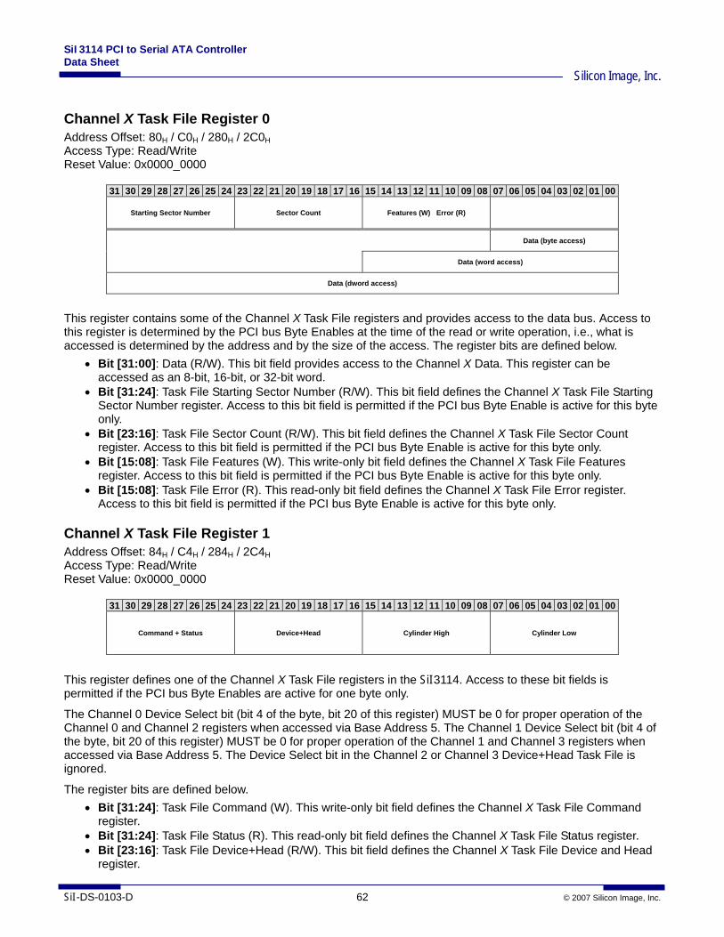
SiI3114 PCI to Serial ATA Controller Data Sheet
Silicon Image, Inc.
SiI-DS-0103-D 62 © 2007 Silicon Image, Inc.
Channel X Task File Register 0 Address Offset: 80H / C0H / 280H / 2C0H Access Type: Read/Write Reset Value: 0x0000_0000
31 30 29 28 27 26 25 24 23 22 21 20 19 18 17 16 15 14 13 12 11 10 09 08 07 06 05 04 03 02 01 00
Starting Sector Number Sector Count Features (W) Error (R)
Data (byte access)
Data (word access)
Data (dword access)
This register contains some of the Channel X Task File registers and provides access to the data bus. Access to this register is determined by the PCI bus Byte Enables at the time of the read or write operation, i.e., what is accessed is determined by the address and by the size of the access. The register bits are defined below.
• Bit [31:00]: Data (R/W). This bit field provides access to the Channel X Data. This register can be accessed as an 8-bit, 16-bit, or 32-bit word.
• Bit [31:24]: Task File Starting Sector Number (R/W). This bit field defines the Channel X Task File Starting Sector Number register. Access to this bit field is permitted if the PCI bus Byte Enable is active for this byte only.
• Bit [23:16]: Task File Sector Count (R/W). This bit field defines the Channel X Task File Sector Count register. Access to this bit field is permitted if the PCI bus Byte Enable is active for this byte only.
• Bit [15:08]: Task File Features (W). This write-only bit field defines the Channel X Task File Features register. Access to this bit field is permitted if the PCI bus Byte Enable is active for this byte only.
• Bit [15:08]: Task File Error (R). This read-only bit field defines the Channel X Task File Error register. Access to this bit field is permitted if the PCI bus Byte Enable is active for this byte only.
Channel X Task File Register 1 Address Offset: 84H / C4H / 284H / 2C4H Access Type: Read/Write Reset Value: 0x0000_0000
31 30 29 28 27 26 25 24 23 22 21 20 19 18 17 16 15 14 13 12 11 10 09 08 07 06 05 04 03 02 01 00
Command + Status Device+Head Cylinder High Cylinder Low
This register defines one of the Channel X Task File registers in the SiI3114. Access to these bit fields is permitted if the PCI bus Byte Enables are active for one byte only.
The Channel 0 Device Select bit (bit 4 of the byte, bit 20 of this register) MUST be 0 for proper operation of the Channel 0 and Channel 2 registers when accessed via Base Address 5. The Channel 1 Device Select bit (bit 4 of the byte, bit 20 of this register) MUST be 0 for proper operation of the Channel 1 and Channel 3 registers when accessed via Base Address 5. The Device Select bit in the Channel 2 or Channel 3 Device+Head Task File is ignored.
The register bits are defined below. • Bit [31:24]: Task File Command (W). This write-only bit field defines the Channel X Task File Command
register. • Bit [31:24]: Task File Status (R). This read-only bit field defines the Channel X Task File Status register. • Bit [23:16]: Task File Device+Head (R/W). This bit field defines the Channel X Task File Device and Head
register.
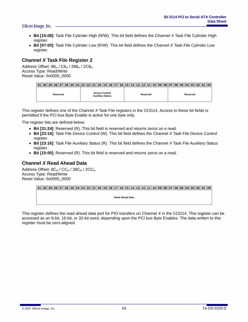
SiI3114 PCI to Serial ATA Controller Data Sheet
Silicon Image, Inc.
© 2007 Silicon Image, Inc. 63 SiI-DS-0103-D
• Bit [15:08]: Task File Cylinder High (R/W). This bit field defines the Channel X Task File Cylinder High register.
• Bit [07:00]: Task File Cylinder Low (R/W). This bit field defines the Channel X Task File Cylinder Low register.
Channel X Task File Register 2 Address Offset: 88H / C8H / 288H / 2C8H Access Type: Read/Write Reset Value: 0x0000_0000
31 30 29 28 27 26 25 24 23 22 21 20 19 18 17 16 15 14 13 12 11 10 09 08 07 06 05 04 03 02 01 00
Reserved Device Control Auxiliary Status Reserved Reserved
This register defines one of the Channel X Task File registers in the SiI3114. Access to these bit fields is permitted if the PCI bus Byte Enable is active for one byte only.
The register bits are defined below. • Bit [31:24]: Reserved (R). This bit field is reserved and returns zeros on a read. • Bit [23:16]: Task File Device Control (W). This bit field defines the Channel X Task File Device Control
register. • Bit [23:16]: Task File Auxiliary Status (R). This bit field defines the Channel X Task File Auxiliary Status
register. • Bit [15:00]: Reserved (R). This bit field is reserved and returns zeros on a read.
Channel X Read Ahead Data Address Offset: 8CH / CCH / 28CH / 2CCH Access Type: Read/Write Reset Value: 0x0000_0000
31 30 29 28 27 26 25 24 23 22 21 20 19 18 17 16 15 14 13 12 11 10 09 08 07 06 05 04 03 02 01 00
Read Ahead Data
This register defines the read ahead data port for PIO transfers on Channel X in the SiI3114. This register can be accessed as an 8-bit, 16-bit, or 32-bit word, depending upon the PCI bus Byte Enables. The data written to this register must be zero-aligned.
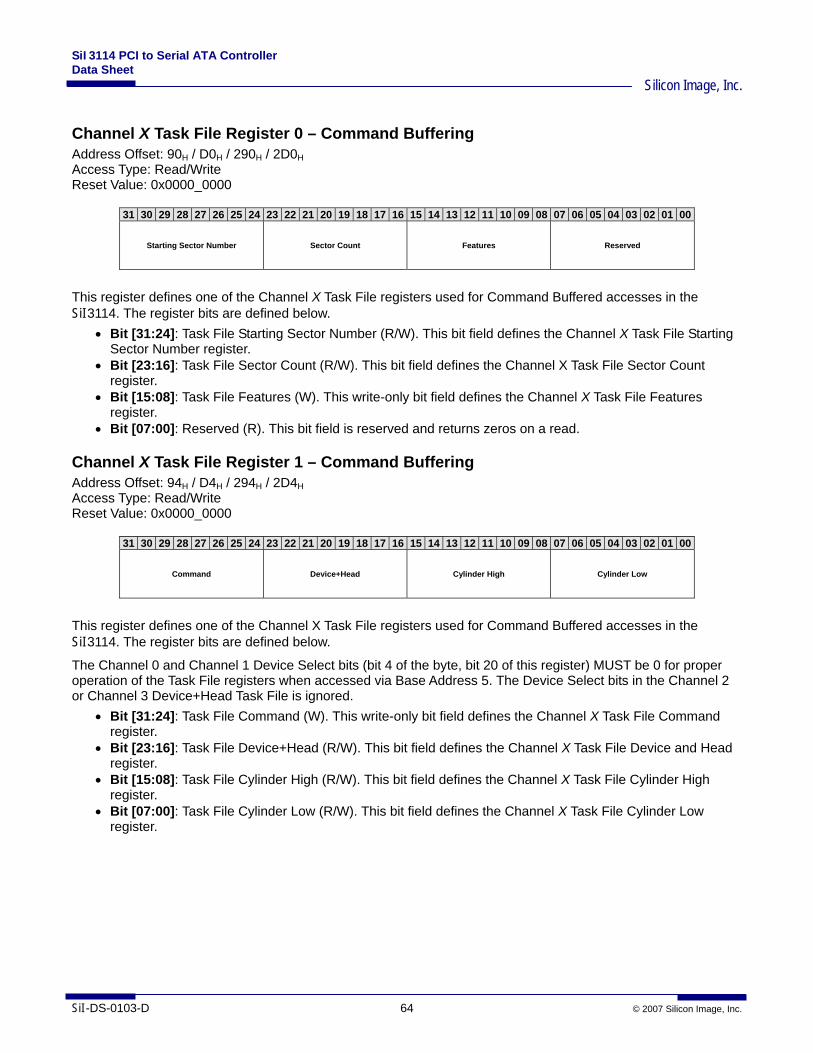
SiI3114 PCI to Serial ATA Controller Data Sheet
Silicon Image, Inc.
SiI-DS-0103-D 64 © 2007 Silicon Image, Inc.
Channel X Task File Register 0 – Command Buffering Address Offset: 90H / D0H / 290H / 2D0H Access Type: Read/Write Reset Value: 0x0000_0000
31 30 29 28 27 26 25 24 23 22 21 20 19 18 17 16 15 14 13 12 11 10 09 08 07 06 05 04 03 02 01 00
Starting Sector Number Sector Count Features Reserved
This register defines one of the Channel X Task File registers used for Command Buffered accesses in the SiI3114. The register bits are defined below.
• Bit [31:24]: Task File Starting Sector Number (R/W). This bit field defines the Channel X Task File Starting Sector Number register.
• Bit [23:16]: Task File Sector Count (R/W). This bit field defines the Channel X Task File Sector Count register.
• Bit [15:08]: Task File Features (W). This write-only bit field defines the Channel X Task File Features register.
• Bit [07:00]: Reserved (R). This bit field is reserved and returns zeros on a read.
Channel X Task File Register 1 – Command Buffering Address Offset: 94H / D4H / 294H / 2D4H Access Type: Read/Write Reset Value: 0x0000_0000
31 30 29 28 27 26 25 24 23 22 21 20 19 18 17 16 15 14 13 12 11 10 09 08 07 06 05 04 03 02 01 00
Command Device+Head Cylinder High Cylinder Low
This register defines one of the Channel X Task File registers used for Command Buffered accesses in the SiI3114. The register bits are defined below.
The Channel 0 and Channel 1 Device Select bits (bit 4 of the byte, bit 20 of this register) MUST be 0 for proper operation of the Task File registers when accessed via Base Address 5. The Device Select bits in the Channel 2 or Channel 3 Device+Head Task File is ignored.
• Bit [31:24]: Task File Command (W). This write-only bit field defines the Channel X Task File Command register.
• Bit [23:16]: Task File Device+Head (R/W). This bit field defines the Channel X Task File Device and Head register.
• Bit [15:08]: Task File Cylinder High (R/W). This bit field defines the Channel X Task File Cylinder High register.
• Bit [07:00]: Task File Cylinder Low (R/W). This bit field defines the Channel X Task File Cylinder Low register.
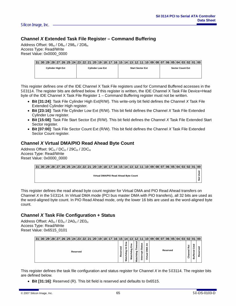
SiI3114 PCI to Serial ATA Controller Data Sheet
Silicon Image, Inc.
© 2007 Silicon Image, Inc. 65 SiI-DS-0103-D
Channel X Extended Task File Register – Command Buffering Address Offset: 98H / D8H / 298H / 2D8H Access Type: Read/Write Reset Value: 0x0000_0000
31 30 29 28 27 26 25 24 23 22 21 20 19 18 17 16 15 14 13 12 11 10 09 08 07 06 05 04 03 02 01 00
Cylinder High Ext Cylinder Low Ext Start Sector Ext Sector Count Ext
This register defines one of the IDE Channel X Task File registers used for Command Buffered accesses in the SiI3114. The register bits are defined below. If this register is written, the IDE Channel X Task File Device+Head byte of the IDE Channel X Task File Register 1 – Command Buffering register must not be written.
• Bit [31:24]: Task File Cylinder High Ext(R/W). This write-only bit field defines the Channel X Task File Extended Cylinder High register.
• Bit [23:16]: Task File Cylinder Low Ext (R/W). This bit field defines the Channel X Task File Extended Cylinder Low register.
• Bit [15:08]: Task File Start Sector Ext (R/W). This bit field defines the Channel X Task File Extended Start Sector register.
• Bit [07:00]: Task File Sector Count Ext (R/W). This bit field defines the Channel X Task File Extended Sector Count register.
Channel X Virtual DMA/PIO Read Ahead Byte Count Address Offset: 9CH / DCH / 29CH / 2DCH Access Type: Read/Write Reset Value: 0x0000_0000
31 30 29 28 27 26 25 24 23 22 21 20 19 18 17 16 15 14 13 12 11 10 09 08 07 06 05 04 03 02 01 00
Virtual DMA/PIO Read Ahead Byte Count
Not
Use
d
This register defines the read ahead byte count register for Virtual DMA and PIO Read Ahead transfers on Channel X in the SiI3114. In Virtual DMA mode (PCI bus master DMA with PIO transfers), all 32 bits are used as the word-aligned byte count. In PIO Read Ahead mode, only the lower 16 bits are used as the word-aligned byte count.
Channel X Task File Configuration + Status Address Offset: A0H / E0H / 2A0H / 2E0H Access Type: Read/Write Reset Value: 0x6515_0101
31 30 29 28 27 26 25 24 23 22 21 20 19 18 17 16 15 14 13 12 11 10 09 08 07 06 05 04 03 02 01 00
Reserved
Res
erve
d
Wat
chdo
g In
t Ena
Wat
chdo
g En
a
Wat
chdo
g Ti
meo
ut
Inte
rrup
t Sta
tus
Virt
ual D
MA
Int
Reserved
Cha
nnel
Rst
Buf
fere
d C
md
Res
erve
d
This register defines the task file configuration and status register for Channel X in the SiI3114. The register bits are defined below.
• Bit [31:16]: Reserved (R). This bit field is reserved and defaults to 0x6515.
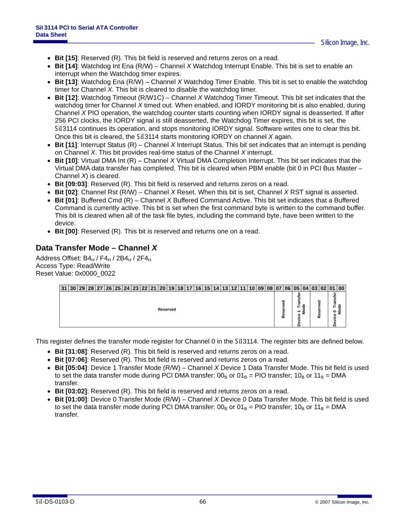
SiI3114 PCI to Serial ATA Controller Data Sheet
Silicon Image, Inc.
SiI-DS-0103-D 66 © 2007 Silicon Image, Inc.
• Bit [15]: Reserved (R). This bit field is reserved and returns zeros on a read. • Bit [14]: Watchdog Int Ena (R/W) – Channel X Watchdog Interrupt Enable. This bit is set to enable an
interrupt when the Watchdog timer expires. • Bit [13]: Watchdog Ena (R/W) – Channel X Watchdog Timer Enable. This bit is set to enable the watchdog
timer for Channel X. This bit is cleared to disable the watchdog timer. • Bit [12]: Watchdog Timeout (R/W1C) – Channel X Watchdog Timer Timeout. This bit set indicates that the
watchdog timer for Channel X timed out. When enabled, and IORDY monitoring bit is also enabled, during Channel X PIO operation, the watchdog counter starts counting when IORDY signal is deasserted. If after 256 PCI clocks, the IORDY signal is still deasserted, the Watchdog Timer expires, this bit is set, the SiI3114 continues its operation, and stops monitoring IORDY signal. Software writes one to clear this bit. Once this bit is cleared, the SiI3114 starts monitoring IORDY on channel X again.
• Bit [11]: Interrupt Status (R) – Channel X Interrupt Status. This bit set indicates that an interrupt is pending on Channel X. This bit provides real-time status of the Channel X interrupt.
• Bit [10]: Virtual DMA Int (R) – Channel X Virtual DMA Completion Interrupt. This bit set indicates that the Virtual DMA data transfer has completed. This bit is cleared when PBM enable (bit 0 in PCI Bus Master – Channel X) is cleared.
• Bit [09:03]: Reserved (R). This bit field is reserved and returns zeros on a read. • Bit [02]: Channel Rst (R/W) – Channel X Reset. When this bit is set, Channel X RST signal is asserted. • Bit [01]: Buffered Cmd (R) – Channel X Buffered Command Active. This bit set indicates that a Buffered
Command is currently active. This bit is set when the first command byte is written to the command buffer. This bit is cleared when all of the task file bytes, including the command byte, have been written to the device.
• Bit [00]: Reserved (R). This bit is reserved and returns one on a read.
Data Transfer Mode – Channel X Address Offset: B4H / F4H / 2B4H / 2F4H Access Type: Read/Write Reset Value: 0x0000_0022
31 30 29 28 27 26 25 24 23 22 21 20 19 18 17 16 15 14 13 12 11 10 09 08 07 06 05 04 03 02 01 00
Reserved
Res
erve
d
Dev
ice
1 T
rans
fer
Mod
e
Res
erve
d
Dev
ice
0 T
rans
fer
Mod
e This register defines the transfer mode register for Channel 0 in the SiI3114. The register bits are defined below.
• Bit [31:08]: Reserved (R). This bit field is reserved and returns zeros on a read. • Bit [07:06]: Reserved (R). This bit field is reserved and returns zeros on a read. • Bit [05:04]: Device 1 Transfer Mode (R/W) – Channel X Device 1 Data Transfer Mode. This bit field is used
to set the data transfer mode during PCI DMA transfer: 00B or 01B = PIO transfer; 10B or 11B = DMA transfer.
• Bit [03:02]: Reserved (R). This bit field is reserved and returns zeros on a read. • Bit [01:00]: Device 0 Transfer Mode (R/W) – Channel X Device 0 Data Transfer Mode. This bit field is used
to set the data transfer mode during PCI DMA transfer: 00B or 01B = PIO transfer; 10B or 11B = DMA transfer.
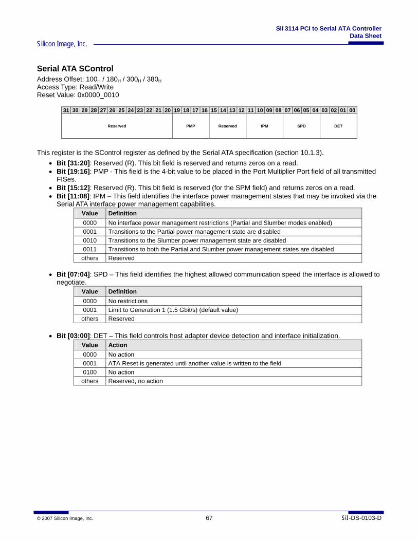
SiI3114 PCI to Serial ATA Controller Data Sheet
Silicon Image, Inc.
© 2007 Silicon Image, Inc. 67 SiI-DS-0103-D
Serial ATA SControl Address Offset: 100H / 180H / 300H / 380H Access Type: Read/Write Reset Value: 0x0000_0010
31 30 29 28 27 26 25 24 23 22 21 20 19 18 17 16 15 14 13 12 11 10 09 08 07 06 05 04 03 02 01 00
Reserved PMP Reserved IPM SPD DET
This register is the SControl register as defined by the Serial ATA specification (section 10.1.3).
• Bit [31:20]: Reserved (R). This bit field is reserved and returns zeros on a read. • Bit [19:16]: PMP - This field is the 4-bit value to be placed in the Port Multiplier Port field of all transmitted
FISes. • Bit [15:12]: Reserved (R). This bit field is reserved (for the SPM field) and returns zeros on a read. • Bit [11:08]: IPM – This field identifies the interface power management states that may be invoked via the
Serial ATA interface power management capabilities. Value Definition 0000 No interface power management restrictions (Partial and Slumber modes enabled) 0001 Transitions to the Partial power management state are disabled 0010 Transitions to the Slumber power management state are disabled 0011 Transitions to both the Partial and Slumber power management states are disabled
others Reserved
• Bit [07:04]: SPD – This field identifies the highest allowed communication speed the interface is allowed to negotiate.
Value Definition 0000 No restrictions 0001 Limit to Generation 1 (1.5 Gbit/s) (default value)
others Reserved
• Bit [03:00]: DET – This field controls host adapter device detection and interface initialization. Value Action 0000 No action 0001 ATA Reset is generated until another value is written to the field 0100 No action
others Reserved, no action
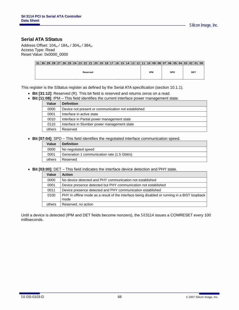
SiI3114 PCI to Serial ATA Controller Data Sheet
Silicon Image, Inc.
SiI-DS-0103-D 68 © 2007 Silicon Image, Inc.
Serial ATA SStatus Address Offset: 104H / 184H / 304H / 384H Access Type: Read Reset Value: 0x0000_0000
31 30 29 28 27 26 25 24 23 22 21 20 19 18 17 16 15 14 13 12 11 10 09 08 07 06 05 04 03 02 01 00
Reserved IPM SPD DET
This register is the SStatus register as defined by the Serial ATA specification (section 10.1.1).
• Bit [31:12]: Reserved (R). This bit field is reserved and returns zeros on a read. • Bit [11:08]: IPM – This field identifies the current interface power management state.
Value Definition 0000 Device not present or communication not established 0001 Interface in active state 0010 Interface in Partial power management state 0110 Interface in Slumber power management state
others Reserved
• Bit [07:04]: SPD – This field identifies the negotiated interface communication speed. Value Definition 0000 No negotiated speed 0001 Generation 1 communication rate (1.5 Gbit/s)
others Reserved
• Bit [03:00]: DET – This field indicates the interface device detection and PHY state. Value Action 0000 No device detected and PHY communication not established 0001 Device presence detected but PHY communication not established 0011 Device presence detected and PHY communication established 0100 PHY in offline mode as a result of the interface being disabled or running in a BIST loopback
mode others Reserved, no action
Until a device is detected (IPM and DET fields become nonzero), the SiI3114 issues a COMRESET every 100 milliseconds.
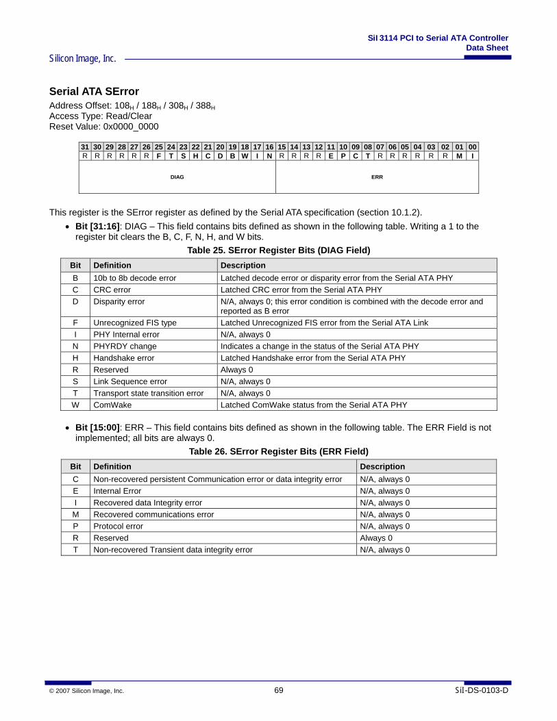
SiI3114 PCI to Serial ATA Controller Data Sheet
Silicon Image, Inc.
© 2007 Silicon Image, Inc. 69 SiI-DS-0103-D
Serial ATA SError Address Offset: 108H / 188H / 308H / 388H Access Type: Read/Clear Reset Value: 0x0000_0000
31 30 29 28 27 26 25 24 23 22 21 20 19 18 17 16 15 14 13 12 11 10 09 08 07 06 05 04 03 02 01 00R R R R R R F T S H C D B W I N R R R R E P C T R R R R R R M I
DIAG ERR
This register is the SError register as defined by the Serial ATA specification (section 10.1.2).
• Bit [31:16]: DIAG – This field contains bits defined as shown in the following table. Writing a 1 to the register bit clears the B, C, F, N, H, and W bits.
Table 25. SError Register Bits (DIAG Field) Bit Definition Description B 10b to 8b decode error Latched decode error or disparity error from the Serial ATA PHY C CRC error Latched CRC error from the Serial ATA PHY D Disparity error N/A, always 0; this error condition is combined with the decode error and
reported as B error F Unrecognized FIS type Latched Unrecognized FIS error from the Serial ATA Link I PHY Internal error N/A, always 0 N PHYRDY change Indicates a change in the status of the Serial ATA PHY H Handshake error Latched Handshake error from the Serial ATA PHY R Reserved Always 0 S Link Sequence error N/A, always 0 T Transport state transition error N/A, always 0 W ComWake Latched ComWake status from the Serial ATA PHY
• Bit [15:00]: ERR – This field contains bits defined as shown in the following table. The ERR Field is not
implemented; all bits are always 0. Table 26. SError Register Bits (ERR Field)
Bit Definition Description C Non-recovered persistent Communication error or data integrity error N/A, always 0 E Internal Error N/A, always 0 I Recovered data Integrity error N/A, always 0 M Recovered communications error N/A, always 0 P Protocol error N/A, always 0 R Reserved Always 0 T Non-recovered Transient data integrity error N/A, always 0
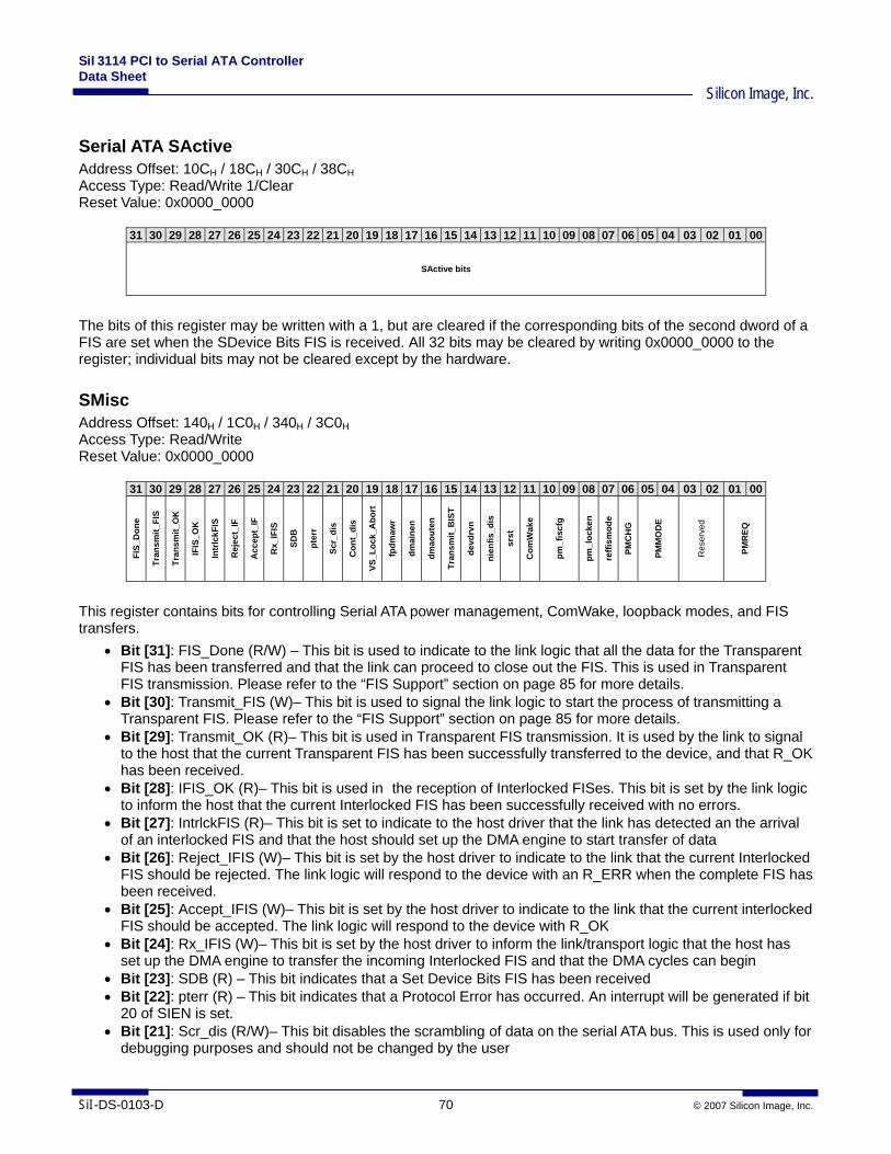
SiI3114 PCI to Serial ATA Controller Data Sheet
Silicon Image, Inc.
SiI-DS-0103-D 70 © 2007 Silicon Image, Inc.
Serial ATA SActive Address Offset: 10CH / 18CH / 30CH / 38CH Access Type: Read/Write 1/Clear Reset Value: 0x0000_0000
31 30 29 28 27 26 25 24 23 22 21 20 19 18 17 16 15 14 13 12 11 10 09 08 07 06 05 04 03 02 01 00
SActive bits
The bits of this register may be written with a 1, but are cleared if the corresponding bits of the second dword of a FIS are set when the SDevice Bits FIS is received. All 32 bits may be cleared by writing 0x0000_0000 to the register; individual bits may not be cleared except by the hardware.
SMisc Address Offset: 140H / 1C0H / 340H / 3C0H Access Type: Read/Write Reset Value: 0x0000_0000
31 30 29 28 27 26 25 24 23 22 21 20 19 18 17 16 15 14 13 12 11 10 09 08 07 06 05 04 03 02 01 00
FIS_
Don
e
Tran
smit_
FIS
Tran
smit_
OK
IFIS
_OK
Intr
lckF
IS
Rej
ect_
IF
Acc
ept_
IF
Rx_
IFIS
SDB
pter
r
Scr_
dis
Con
t_di
s
VS_L
ock_
Abo
rt
fpdm
awr
dmai
nen
dmao
uten
Tran
smit_
BIS
T
devd
rvn
nien
fis_d
is
srst
Com
Wak
e
pm_f
iscf
g
pm_l
ocke
n
reffi
smod
e
PMC
HG
PMM
OD
E
Res
erve
d
PMR
EQ
This register contains bits for controlling Serial ATA power management, ComWake, loopback modes, and FIS transfers.
• Bit [31]: FIS_Done (R/W) – This bit is used to indicate to the link logic that all the data for the Transparent FIS has been transferred and that the link can proceed to close out the FIS. This is used in Transparent FIS transmission. Please refer to the “FIS Support” section on page 85 for more details.
• Bit [30]: Transmit_FIS (W)– This bit is used to signal the link logic to start the process of transmitting a Transparent FIS. Please refer to the “FIS Support” section on page 85 for more details.
• Bit [29]: Transmit_OK (R)– This bit is used in Transparent FIS transmission. It is used by the link to signal to the host that the current Transparent FIS has been successfully transferred to the device, and that R_OK has been received.
• Bit [28]: IFIS_OK (R)– This bit is used in the reception of Interlocked FISes. This bit is set by the link logic to inform the host that the current Interlocked FIS has been successfully received with no errors.
• Bit [27]: IntrlckFIS (R)– This bit is set to indicate to the host driver that the link has detected an the arrival of an interlocked FIS and that the host should set up the DMA engine to start transfer of data
• Bit [26]: Reject_IFIS (W)– This bit is set by the host driver to indicate to the link that the current Interlocked FIS should be rejected. The link logic will respond to the device with an R_ERR when the complete FIS has been received.
• Bit [25]: Accept_IFIS (W)– This bit is set by the host driver to indicate to the link that the current interlocked FIS should be accepted. The link logic will respond to the device with R_OK
• Bit [24]: Rx_IFIS (W)– This bit is set by the host driver to inform the link/transport logic that the host has set up the DMA engine to transfer the incoming Interlocked FIS and that the DMA cycles can begin
• Bit [23]: SDB (R) – This bit indicates that a Set Device Bits FIS has been received • Bit [22]: pterr (R) – This bit indicates that a Protocol Error has occurred. An interrupt will be generated if bit
20 of SIEN is set. • Bit [21]: Scr_dis (R/W)– This bit disables the scrambling of data on the serial ATA bus. This is used only for
debugging purposes and should not be changed by the user
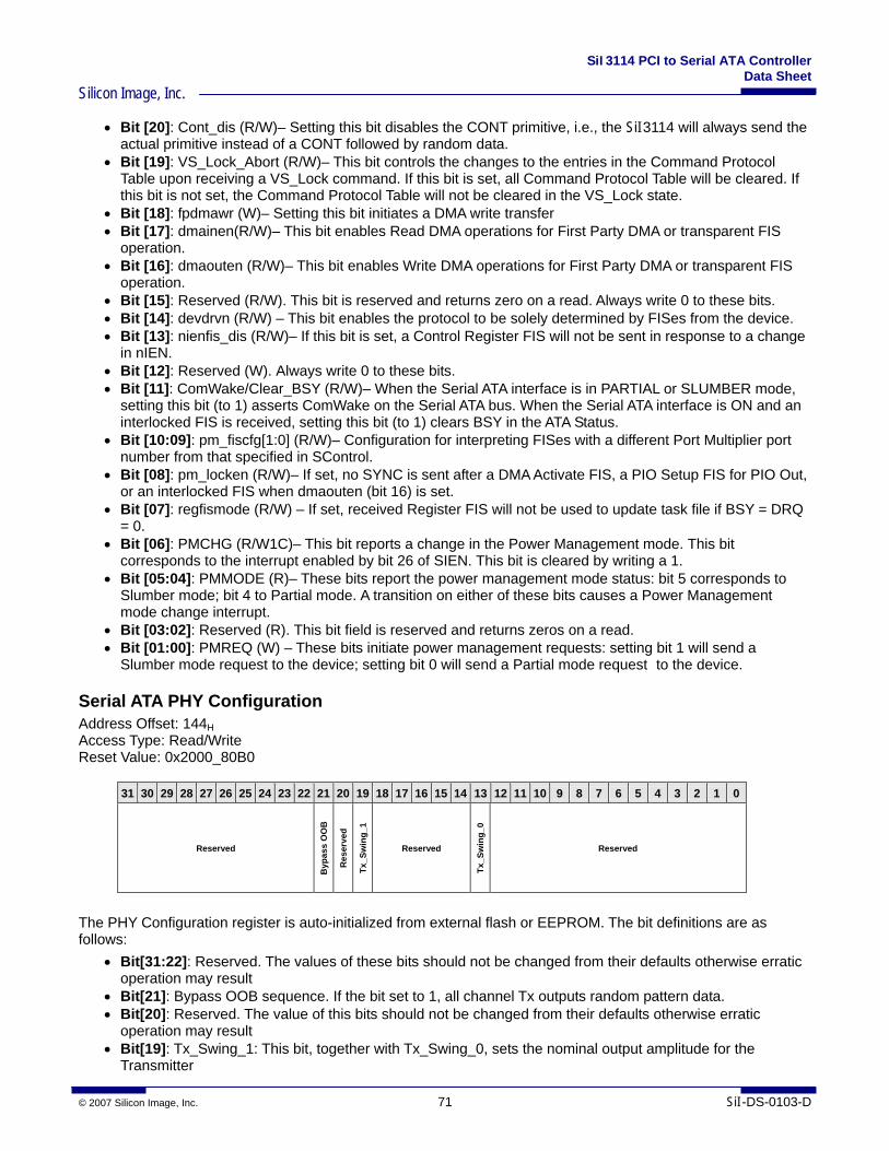
SiI3114 PCI to Serial ATA Controller Data Sheet
Silicon Image, Inc.
© 2007 Silicon Image, Inc. 71 SiI-DS-0103-D
• Bit [20]: Cont_dis (R/W)– Setting this bit disables the CONT primitive, i.e., the SiI3114 will always send the actual primitive instead of a CONT followed by random data.
• Bit [19]: VS_Lock_Abort (R/W)– This bit controls the changes to the entries in the Command Protocol Table upon receiving a VS_Lock command. If this bit is set, all Command Protocol Table will be cleared. If this bit is not set, the Command Protocol Table will not be cleared in the VS_Lock state.
• Bit [18]: fpdmawr (W)– Setting this bit initiates a DMA write transfer • Bit [17]: dmainen(R/W)– This bit enables Read DMA operations for First Party DMA or transparent FIS
operation. • Bit [16]: dmaouten (R/W)– This bit enables Write DMA operations for First Party DMA or transparent FIS
operation. • Bit [15]: Reserved (R/W). This bit is reserved and returns zero on a read. Always write 0 to these bits. • Bit [14]: devdrvn (R/W) – This bit enables the protocol to be solely determined by FISes from the device. • Bit [13]: nienfis_dis (R/W)– If this bit is set, a Control Register FIS will not be sent in response to a change
in nIEN. • Bit [12]: Reserved (W). Always write 0 to these bits. • Bit [11]: ComWake/Clear_BSY (R/W)– When the Serial ATA interface is in PARTIAL or SLUMBER mode,
setting this bit (to 1) asserts ComWake on the Serial ATA bus. When the Serial ATA interface is ON and an interlocked FIS is received, setting this bit (to 1) clears BSY in the ATA Status.
• Bit [10:09]: pm_fiscfg[1:0] (R/W)– Configuration for interpreting FISes with a different Port Multiplier port number from that specified in SControl.
• Bit [08]: pm_locken (R/W)– If set, no SYNC is sent after a DMA Activate FIS, a PIO Setup FIS for PIO Out, or an interlocked FIS when dmaouten (bit 16) is set.
• Bit [07]: regfismode (R/W) – If set, received Register FIS will not be used to update task file if BSY = DRQ = 0.
• Bit [06]: PMCHG (R/W1C)– This bit reports a change in the Power Management mode. This bit corresponds to the interrupt enabled by bit 26 of SIEN. This bit is cleared by writing a 1.
• Bit [05:04]: PMMODE (R)– These bits report the power management mode status: bit 5 corresponds to Slumber mode; bit 4 to Partial mode. A transition on either of these bits causes a Power Management mode change interrupt.
• Bit [03:02]: Reserved (R). This bit field is reserved and returns zeros on a read. • Bit [01:00]: PMREQ (W) – These bits initiate power management requests: setting bit 1 will send a
Slumber mode request to the device; setting bit 0 will send a Partial mode request to the device.
Serial ATA PHY Configuration Address Offset: 144H Access Type: Read/Write Reset Value: 0x2000_80B0
31 30 29 28 27 26 25 24 23 22 21 20 19 18 17 16 15 14 13 12 11 10 9 8 7 6 5 4 3 2 1 0
Reserved
Byp
ass
OO
B
Res
erve
d
Tx_S
win
g_1
Reserved
Tx_S
win
g_0
Reserved
The PHY Configuration register is auto-initialized from external flash or EEPROM. The bit definitions are as follows:
• Bit[31:22]: Reserved. The values of these bits should not be changed from their defaults otherwise erratic operation may result
• Bit[21]: Bypass OOB sequence. If the bit set to 1, all channel Tx outputs random pattern data. • Bit[20]: Reserved. The value of this bits should not be changed from their defaults otherwise erratic
operation may result • Bit[19]: Tx_Swing_1: This bit, together with Tx_Swing_0, sets the nominal output amplitude for the
Transmitter
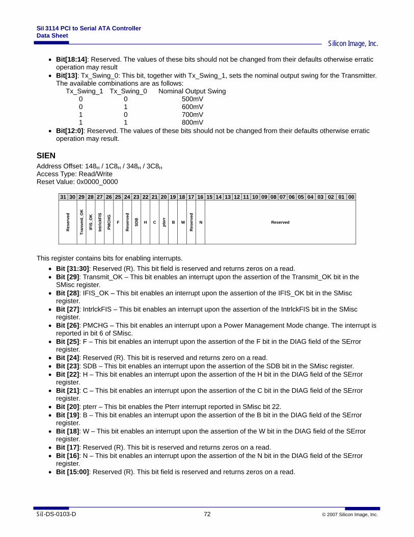
SiI3114 PCI to Serial ATA Controller Data Sheet
Silicon Image, Inc.
SiI-DS-0103-D 72 © 2007 Silicon Image, Inc.
• Bit[18:14]: Reserved. The values of these bits should not be changed from their defaults otherwise erratic operation may result
• Bit[13]: Tx_Swing_0: This bit, together with Tx_Swing_1, sets the nominal output swing for the Transmitter. The available combinations are as follows:
Tx_Swing_1 Tx_Swing_0 Nominal Output Swing 0 0 500mV 0 1 600mV 1 0 700mV 1 1 800mV
• Bit[12:0]: Reserved. The values of these bits should not be changed from their defaults otherwise erratic operation may result.
SIEN Address Offset: 148H / 1C8H / 348H / 3C8H Access Type: Read/Write Reset Value: 0x0000_0000
31 30 29 28 27 26 25 24 23 22 21 20 19 18 17 16 15 14 13 12 11 10 09 08 07 06 05 04 03 02 01 00
Res
erve
d
Tran
smit_
OK
IFIS
_OK
Intr
lckF
IS
PMC
HG
F
Res
erve
d
SDB
H C
pter
r
B W
Res
erve
d
N Reserved
This register contains bits for enabling interrupts.
• Bit [31:30]: Reserved (R). This bit field is reserved and returns zeros on a read. • Bit [29]: Transmit_OK – This bit enables an interrupt upon the assertion of the Transmit_OK bit in the
SMisc register. • Bit [28]: IFIS_OK – This bit enables an interrupt upon the assertion of the IFIS_OK bit in the SMisc
register. • Bit [27]: IntrlckFIS – This bit enables an interrupt upon the assertion of the IntrlckFIS bit in the SMisc
register. • Bit [26]: PMCHG – This bit enables an interrupt upon a Power Management Mode change. The interrupt is
reported in bit 6 of SMisc. • Bit [25]: F – This bit enables an interrupt upon the assertion of the F bit in the DIAG field of the SError
register. • Bit [24]: Reserved (R). This bit is reserved and returns zero on a read. • Bit [23]: SDB – This bit enables an interrupt upon the assertion of the SDB bit in the SMisc register. • Bit [22]: H – This bit enables an interrupt upon the assertion of the H bit in the DIAG field of the SError
register. • Bit [21]: C – This bit enables an interrupt upon the assertion of the C bit in the DIAG field of the SError
register. • Bit [20]: pterr – This bit enables the Pterr interrupt reported in SMisc bit 22. • Bit [19]: B – This bit enables an interrupt upon the assertion of the B bit in the DIAG field of the SError
register. • Bit [18]: W – This bit enables an interrupt upon the assertion of the W bit in the DIAG field of the SError
register. • Bit [17]: Reserved (R). This bit is reserved and returns zeros on a read. • Bit [16]: N – This bit enables an interrupt upon the assertion of the N bit in the DIAG field of the SError
register. • Bit [15:00]: Reserved (R). This bit field is reserved and returns zeros on a read.
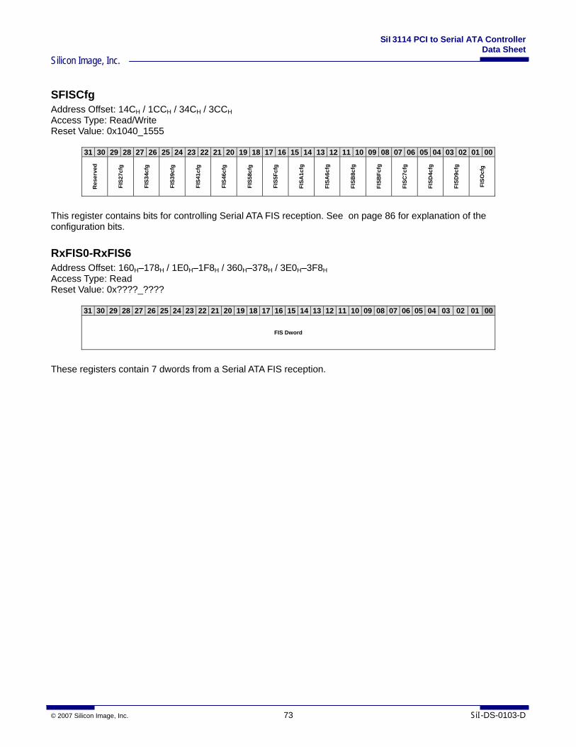
SiI3114 PCI to Serial ATA Controller Data Sheet
Silicon Image, Inc.
© 2007 Silicon Image, Inc. 73 SiI-DS-0103-D
SFISCfg Address Offset: 14CH / 1CCH / 34CH / 3CCH Access Type: Read/Write Reset Value: 0x1040_1555
31 30 29 28 27 26 25 24 23 22 21 20 19 18 17 16 15 14 13 12 11 10 09 08 07 06 05 04 03 02 01 00
Res
erve
d
FIS2
7cfg
FIS3
4cfg
FIS3
9cfg
FIS4
1cfg
FIS4
6cfg
FIS5
8cfg
FIS5
Fcfg
FISA
1cfg
FISA
6cfg
FISB
8cfg
FISB
Fcfg
FISC
7cfg
FISD
4cfg
FISD
9cfg
FISO
cfg
This register contains bits for controlling Serial ATA FIS reception. See on page 86 for explanation of the configuration bits.
RxFIS0-RxFIS6 Address Offset: 160H–178H / 1E0H–1F8H / 360H–378H / 3E0H–3F8H Access Type: Read Reset Value: 0x????_????
31 30 29 28 27 26 25 24 23 22 21 20 19 18 17 16 15 14 13 12 11 10 09 08 07 06 05 04 03 02 01 00
FIS Dword
These registers contain 7 dwords from a Serial ATA FIS reception.
SiI3114 PCI to Serial ATA Controller Data Sheet
Silicon Image, Inc.
SiI-DS-0103-D 74 © 2007 Silicon Image, Inc.
Programming Sequences The programming sequence for the SiI3114 is about the same as for the SiI3112 or SiI3512. However, SiI3114 supports up to four SATA devices (instead of two for the others).
In order to minimize the legacy BIOS code changes, the SiI3114 uses “Master/Slave” type of emulation for the register mapping of Base Address Register 0 ~ 4 (between SATA device 0 and device 2 or SATA device 1 and device 3). Therefore, the programmer will not be able to access SATA device 0 and device 2 (or device 1 and device 3) at the same time when BAR 0~4 are used to access the devices. SATA device 0 is equivalent to legacy Primary Master device, SATA device 1 is equivalent to legacy Secondary Master device, SATA device 2 is equivalent to legacy Primary Slave device, and SATA device 3 is equivalent to legacy Secondary Slave device.
In order to access all four SATA devices simultaneously, BAR5 registers must be used. They have a similar structure to the previous 2 channel controllers for the first 512 bytes (for device 0 and device 1), but they have an additional 512 bytes of registers to duplicate the register structures for the additional two SATA channels (device 2 and device 3).
When BAR5 registers are used to access all four SATA devices simultaneously, the interrupt steering bit at bit 1 in BAR5 offset 200h must be set. The interrupt steering bit must be reset when “Master/Slave” type of emulation is used. The reset value for this bit is 0. This bit must be remained set for simultaneous 4 channels operation. Any write operation to the BAR5 offset 200h register should mask the "Interrupt steering" bit and not to reset it by accident.
Recommended Initialization Sequence for the SiI3114 The recommended initialization sequence for the SiI3114 is detailed below.
Initialize PCI Configuration Space registers: • Initialize Base Address Register 0 with the address of an 8-byte range in I/O space. • Initialize Base Address Register 1 with the address of a 4-byte range in I/O space. • Initialize Base Address Register 2 with the address of an 8-byte range in I/O space. • Initialize Base Address Register 3 with the address of a 4-byte range in I/O space. • Initialize Base Address Register 4 with the address of a 16-byte range in I/O space. • Initialize Base Address Register 5 with the address of a 1024-byte range in memory space. • To enable the bios expansion ROM, initialize the Expansion ROM Base Address Register with the address
of a 512KB range in memory space. • Enable I/O space access, memory space access, and bus master operation by setting bits [2:0] of the PCI
Command register. Note: The preceding configuration space register initialization is normally done by the motherboard BIOS in PC type systems.
If the arbiter’s default FIFO read/write request thresholds are not suitable for the application they may be changed via the FIFO Valid Byte Count and Control Channel x register. The read threshold is defined by bits [05:00], and the write threshold is defined by bits [13:08] in the FIFO Valid Byte Count and Control – Channel x register. In most environments, setting these bit fields to zero results in the best utilization of the PCI bus by the SiI3114 controller.
If interrupt driven operation is not desired, set bits [23:22] of the System Configuration Status and Command register to block interrupts from reaching the PCI bus.
SiI3114 PCI to Serial ATA Controller Data Sheet
Silicon Image, Inc.
© 2007 Silicon Image, Inc. 75 SiI-DS-0103-D
Serial ATA Device Initialization This section provides a general overview of the steps necessary to initialize a Serial ATA device before it can be used for read/write operations.
Select the Serial ATA device. The device is selected by programming bits [23:16] in the Channel x Task File Register 1 register. If interrupt driven operation is desired, ensure that interrupts are enabled by writing 0 to bits [23:16] of the Channel x Task File Register 2 register. For ATA Devices Only:
Issue the Initialize Device Parameters command by • Programming bits [23:16] in the Channel x Task File 0 register with the number of
logical sectors per logical track. • Programming bits [23:16] in the Channel x Task File 1 register with the maximum
head number. • Programming bits [31:24] in the Channel x Task File Register 1 register with the
value = 91H. • Wait for the command to complete. This can be accomplished by waiting for an
interrupt if interrupts have been enabled at both the controller and the device. If interrupts are not enabled, command completion can be detected by polling bits [31:24] of the Channel x Task File Register 1 register until the BUSY bit is no longer asserted.
If the device supports read/write multiple commands, issue the Set Multiple Mode command by:
• Programming bits [23:16] in the Channel x Task File 0 register with the number of sectors per block to use on the following Read/Write Multiple commands.
• Programming bits [31:24] in the Channel x Task File Register 1 register with the value = C6H.
• Wait for the command to complete (see above).
For both ATA and ATAPI Devices: Set device transfer mode by:
• Programming bits [15:08] in the Channel x Task File 0 register with the value 03H to “Set the transfer mode based on value in Sector Count Register”.
• Programming bits [23:16] in the Channel x Task File 0 register to the desired transfer mode. The settings are defined below:
08H = PIO Mode 0 09H = PIO Mode 1 0AH = PIO Mode 2 0BH = PIO Mode 3 0CH = PIO Mode 4 20H = Multiword DMA Mode 0 21H = Multiword DMA Mode 1 22H = Multiword DMA Mode 2 40H = Ultra DMA Mode 0 41H = Ultra DMA Mode 1 42H = Ultra DMA Mode 2 43H = Ultra DMA Mode 3 44H = Ultra DMA Mode 4 45H = Ultra DMA Mode 5 46H = Ultra DMA Mode 6
• Programming bits [31:24] in the Channel x Task File Register 1 register with the value = EFH.
• Wait for the command to complete (see above).
SiI3114 PCI to Serial ATA Controller Data Sheet
Silicon Image, Inc.
SiI-DS-0103-D 76 © 2007 Silicon Image, Inc.
In order to use the controller’s DMA capability to perform the data transfer for an ATA/ATAPI command, the controller needs to be configured for the transfer mode to use when transferring data to or from the ATA bus. The data transfer mode is set by programming bits [1:0] of the Channel x Data Transfer Mode register. The transfer mode select values are listed below:
00B = PIO/Virtual DMA Mode (the "interface" between the device and the controller is setup for "PIO mode", but the PCI interface is setup for DMA transfer).
10B = DMA Mode (the "interface" between the device and the controller is setup for "DMA mode", and the PCI interface is also setup for DMA transfer).
Note: If the "interface" between the device and the controller is setup for "PIO mode", and the PCI interface is also setup for PIO transfer, there is no need to change these two bits.
Issue ATA Command The following describes the sequence to issue a read/write type command to an ATA device.
1. Select the device. The device is selected by programming bits [23:16] in the Channel x Task File Register 1 register.
2. Set the number of sectors to be transferred by programming bits [23:16] of the Channel x Task File Register 0 register.
3. Set the location of data to be transferred. The location is defined by programming the following: Bits [31:24] in the Channel x Task File Register 0 register define the Starting Sector. Bits [23:16] in the Channel x Task File Register 1 register define the Device and Head value. Bits [15:08] in the Channel x Task File Register 1 register define the Cylinder High value. Bits [07:00] in the Channel x Task File Register 1 register define the Cylinder Low value.
4. Issue the Read/Write PIO/DMA command by programming bits [31:24] in the Channel x Task File Register 1 register with the command desired.
PIO Mode Read/Write Operation Once the SiI3114 is initialized via the initialization sequence described in the “Recommended Initialization Sequence for the SiI3114” section, the ATA device has been initialized for PIO mode data transfer per the guidelines in the “Serial ATA Device Initialization” section, and the controller channel has been initialized for PIO mode data transfer, PIO read/write operations may be performed by following the programming sequence described below.
Issue a PIO Read/Write command to device following the steps in Issue ATA Command section above.
Read Operation
Wait until a channel interrupt (bit 11 in the Channel x Task File Timing + Configuration + Status register is set).
Read the device status at bits [31:24] in the Channel x Task File Register 1 register to clear the device interrupt and determine if there was error.
If no error, continue to read data via the Channel x Task File Register 0 register, until the expected number of sectors of data per interrupt are read.
Repeat the above three steps until all data for the read command has been transferred or an error has been detected.
Write Operation
Wait until bit 27(DRQ) in the Channel x Task File Register 1 register is set.
Continue to write data via the Channel x Task File Register 0 register until the expected number of sectors of data per interrupt are written.
Wait until a channel interrupt (bit 11 in the Channel x Task File Timing + Configuration + Status register is set).
SiI3114 PCI to Serial ATA Controller Data Sheet
Silicon Image, Inc.
© 2007 Silicon Image, Inc. 77 SiI-DS-0103-D
Read the device status at bits [31:24] in the Channel x Task File Register 1 register to clear the device interrupt and determine if there was error.
If no error, repeat the previous four steps until all data for the write command has been transferred or an error has been detected.
Watchdog Timer Operation The purpose of the watchdog timer is to prevent the host system from hanging because a device operating in PIO mode stopped responding to task file accesses. If, during a task file access by the host, the device negates IORDY and then stops responding, the host will hang waiting for the access to complete. It is this type of hang, that the watchdog timer is designed to protect against.
The watchdog timer monitors the length of time the IORDY signal is negated. If the watchdog timer detects that the IORDY signal has remained negated longer than the watchdog timeout period (approximately 1000 PCI clocks), the watchdog timer will force the task file access cycle to complete, and set the watchdog timeout bit in the Channel x Task File Timing + Configuration + Status register. The data associated with a timed out access should be considered invalid. Additionally, the watchdog timer can be configured to generate an interrupt when a timeout is detected by setting bit 14 of the Channel x Task File Timing + Configuration + Status register.
The watchdog timer feature is disabled by default.
In addition to the controller channel initialization specified previously, add the following two steps to enable the watchdog timer:
• Enable the watchdog timer by setting bit 13 of the Channel x Task File Timing + Config + Status register. • If an interrupt is desired whenever the watchdog times out, enable the watchdog interrupt by setting bit 14
of the Channel x Task File Timing + Config + Status register. The following programming sequences are needed for each PIO Mode Read/Write Operation with the watchdog timer enabled:
Issue a Read/Write PIO Command to the ATA drive following the steps in “Issue ATA Command” section on page 76.
Read Operation
Wait for a channel interrupt. If controller interrupts are disabled, poll for the interrupt by reading the Channel x Task File Timing + Configuration + Status register. If bit 12 is set, a watchdog timeout has occurred. If bit 11 is set, the ATA device is interrupting.
If the watchdog timeout bit is set,
Write 1 to bit 12 in the Channel x Task File Timing + Configuration + Status register to clear watchdog timeout status.
The watchdog timeout represents a fatal error as far as the current ATA command is concerned. A course of action that might be appropriate at this point might be to reset and reinitialize the ATA channel and then retrying the command that failed.
If the ATA device interrupt bit is set,
Read the device status at bits [31:24] in the Channel x Task File Register 1 register to clear the device interrupt and determine if there was an error.
Write 1 to bit 18 of the PCI Bus Master – Channel x Register to clear the ATA interrupt.
If the ATA device is not reporting an error, continue to read data via the Channel x Task File Register 0 register, until the expected number of sectors of data per interrupt are read.
Repeat the read operation steps until all data for the read command has been transferred or an error has been detected.
SiI3114 PCI to Serial ATA Controller Data Sheet
Silicon Image, Inc.
SiI-DS-0103-D 78 © 2007 Silicon Image, Inc.
Write Operation
Wait until bit 27(DRQ) in the Channel x Task File Register 1 register is set.
Continue to write data via the Channel x Task File Register 0 register until the expected number of sectors of data per interrupt are written.
Wait for a channel interrupt.
If controller interrupts are disabled, poll for the interrupt by reading the Channel x Task File Timing + Configuration + Status register. If bit 12 is set, a watchdog timeout has occurred. If bit 11 is set, the ATA device is interrupting.
If the watchdog timeout bit is set,
Write 1 to bit 12 in the Channel x Task File Timing + Configuration + Status register to clear watchdog timeout status.
The watchdog timeout represents a fatal error as far as the current ATA command is concerned. A course of action that might be appropriate at this point might be to reset and reinitialize the ATA channel and then retrying the command that failed.
If the ATA device interrupt bit is set,
Read the device status at bits [31:24] in the Channel x Task File Register 1 register to clear the device interrupt and determine if there was an error.
Write 1 to bit 18 of the PCI Bus Master – Channel x Register to clear the ATA interrupt.
If no error, repeat the write operation steps until all data for the write command has been transferred or an error has been detected.
PIO Mode Read Ahead Operation Read ahead operation allows the controller to “pre-fetch” data and store it in the controller’s channel FIFO, where it will later be retrieved by the host. This mode of operation has the potential to speed-up PIO data transfers by not forcing the host to wait the programmed PIO cycle time for every access to the task file data register. The amount of any speed increase will depend on the PIO mode in use, the characteristics of the host PCI bus, as well as the speed of the host processor.
To use the controller’s PIO read ahead capability, make the following changes to the “Read Operation” portion of the “PIO Mode Read/Write Operation” and “Watchdog Timer Operation” sections:
• Just prior to retrieving the read data, set the read ahead byte count by programming bits [15:00] in the Channel x Virtual DMA/PIO Read Ahead Byte Count register with the exact number of bytes to be read for the interrupt.
• Instead of reading the Channel x Task File Register 0 register to retrieve the data, read the Channel x Read Ahead Data register.
MDMA/UDMA Read/Write Operation Once the SiI3114 is initialized via the initialization sequence described in the “Recommended Initialization Sequence for the SiI3114” section, and the SATA device has been initialized for MDMA/UDMA mode data transfer per the guidelines in the “Serial ATA Device Initialization” section, DMA read/write operations may be performed by following the programming sequence described below.
Issue a DMA read/write command to the device following the steps in the “Issue ATA Command” section on page 76.
Program Bus Master Registers
Clear bit 17 in the PCI Bus Master – Channel x register. This bit is set if an error occurred during the previous DMA access.
Clear bit 18 in the PCI Bus Master – Channel x register. This bit is set if an interrupt occurred during the previous DMA access.
SiI3114 PCI to Serial ATA Controller Data Sheet
Silicon Image, Inc.
© 2007 Silicon Image, Inc. 79 SiI-DS-0103-D
Create a Physical Region Descriptor (PRD) Table.
A PRD table is an array where each entry describes the location and size of a physical memory buffer that will be used during the DMA operation. Each PRD table entry is 64-bits in length, formatted as follows; bits [31:0] contain the 32-bit starting address of the memory buffer, bits [47:32] contain the 16-bit size of the memory buffer, bits [62:48] are normally unused, bit 63 flags the end of the PRD table and therefore should only be set in the last entry of the PRD table. The PRD table itself must be constructed in a memory region that can be directly accessed by the SiI3114 controller. Once the PRD table is built, the controller must be informed of its location. This is accomplished by writing the 32-bit address of the PRD table to the PRD Table Address – Channel x register.
Enable DMA transfer.
DMA is enabled by writing bits [7:0] of the PCI Bus Master – Channel x register. Bit 3 of this register controls the direction of the DMA transfer; 1 = write to memory, 0 = read from memory. Setting bit 0 of the register enables the controller to perform DMA operations. Note: Task file registers are inaccessible as long as bit 0 is set.
Wait for a PCI interrupt.
When a PCI interrupt occurs, read the PCI Master – Channel x status register and check the DMA status bits. The possible combinations of the status bits [18:16] are defined below.
000B = If the device does not report an error, then the PRD table specified a size that is smaller than the transfer size.
001B = DMA transfer in progress.
010B = The controller had a problem transferring data to/from memory.
100B = Normal completion.
101B = If the device does not report an error, then the PRD specified a size that is larger than the transfer size.
Make sure PCI bus master operation of the SiI3114 is stopped by clearing bit 0 of the PCI Bus Master – Channel x register.
Note: The task file registers are not accessible as long as bit 0 is set. Clearing bit 0 causes bit 16 to be cleared as well.
Read the device status at bits [13:24] in the Channel x Task File Register 1 register to clear the device interrupt (and the PCI Interrupt) and determine if there was error.
Write ‘1’ to bit 18 (DMA Comp) in the PCI Bus Master – Channel x register to clear the status.
Virtual DMA Read/Write Operation In virtual DMA operation the controller uses a PIO data transfer mode to move data between an ATA/ATAPI device and the controller, and uses DMA to move that same data between the controller and the host memory. For ATA/ATAPI devices that cannot operate in a “true” DMA mode, virtual DMA provides two benefits; first, using DMA to move data reduces the demand on the host CPU, and second, systems that use virtual memory often require that data buffers that will be accessed directly by low level device drivers be “mapped” into the operating system’s address space, in virtual DMA mode the CPU does not access the data buffer directly, so the overhead of obtaining the mapping to operating system address space is eliminated.
Using Virtual DMA with Non-DMA Capable Devices Once the SiI3114 is initialized via the initialization sequence described in the “Recommended Initialization Sequence for the SiI3114” section, and the ATA device has been initialized for PIO mode data transfer per the guidelines in the “Serial ATA Device Initialization” section, virtual DMA read/write operations may be performed by following the programming sequence described below.
Note: The watchdog timer feature is compatible with virtual DMA operation. See section 0 for details about using the watchdog timer.
SiI3114 PCI to Serial ATA Controller Data Sheet
Silicon Image, Inc.
SiI-DS-0103-D 80 © 2007 Silicon Image, Inc.
Issue a PIO read/write command to the device following the steps in the “Issue ATA Command” section on page 76.
Read Operation
Wait for a PCI interrupt.
Read the DMA status bits [18:16] of the PCI Bus Master – Channel x register, and check that bit 18 is set to make sure the interrupt was generated by the expected channel.
If expected channel interrupted, read bits [11:10] of the channel’s Channel x Task File Timing + Configuration + Status register to determine the cause of the interrupt. Bit 11 is set if the ATA/ATAPI device has an interrupt pending, bit 10 is set if a virtual DMA operation completed.
If a virtual DMA operation completed,
Write 00H to bits [7:0] of the PCI Bus Master – Channel x register to disable DMA operation.
Write 1 to bits [18:17] of the PCI Bus Master –Channel x register to reset the DMA status and virtual DMA interrupt bits, and the PCI interrupt.
Check the previously read DMA status bits to ensure the DMA completed successfully.
Because ATA/ATAPI commands that transfer data using PIO can generate several interrupts during the data transfer phase of the command, a race condition is created between the interrupt indicating the completion of a virtual DMA operation, and the interrupt from the ATA/ATAPI device indicating it is ready to perform the next part of the data transfer. To prevent missing an ATA/ATAPI device interrupt due to this race condition, it is necessary to re-read the channel’s Channel x Task File Timing + Configuration + Status register after disabling DMA operation and examining bit 11. If bit 11 is set, the ATA/ATAPI device is interrupting and should be serviced by following the steps below (assuming that the virtual DMA operation completed successfully).
If the ATA/ATAPI device has interrupted,
Read the device status at bits [31:24] in the Channel x Task File Register 1 register to clear the device interrupt and determine if there was an error.
Write 1 to bit 18 of the PCI Bus Master – Channel x register to clear the DMA Complete bit (NOTE: The DMA Complete bit acts as a latched copy of the ATA interrupt line when the channel is not performing a DMA operation).
If the ATA/ATAPI device is not reporting an error, and DRQ is asserted (bit 27 of Channel x Task File Register 1), then the device is interrupting to transfer data to the host. To transfer the data, the DMA registers are setup to only perform that part of the data transfer expected for this interrupt. The DMA is setup similarly to the way it is when performing a normal read DMA command, but with one additional step. Before the DMA is enabled, the Channel x Virtual DMA/PIO Read Ahead Byte Count register must be written with the 32-bit count of the number of bytes to be transferred for this interrupt.
Repeat the above steps until all data for the read command has been transferred or an error has been detected.
Write Operation
Poll the Channel x Task File Register 1 bits [31:24] until either bit 27 (DRQ) is set indicating the device is ready for write data transfer, or bit 24 (ERR) is set indicating the device has detected an error with the write command.
If no error, and DRQ is asserted (bit 27 of Channel x Task File Register 1), then the device is waiting for write data transfer. To transfer the data, the DMA registers are setup to only perform that part of the data transfer expected at this time. For example, a Write Sectors command would expect to transfer 1 sector (512 bytes), while a Write Multiple command would expect to transfer the lesser of the number of sectors set by the Set Multiple Mode command or the total number of sectors specified by the Write Multiple command. The DMA is setup similarly to the way it is when performing a normal write DMA command, but
SiI3114 PCI to Serial ATA Controller Data Sheet
Silicon Image, Inc.
© 2007 Silicon Image, Inc. 81 SiI-DS-0103-D
with one additional step. Before the DMA is enabled, the Channel x Virtual DMA/PIO Read Ahead Byte Count register must be written with the 32-bit count of the number of bytes to be transferred.
Wait for a PCI interrupt.
Read the DMA status bits [18:16] of the PCI Bus Master – Channel x register, and check that bit 18 is set to make sure the interrupt was generated by the expected channel.
If expected channel interrupted, read bits [11:10] of the Channel x Task File Timing + Configuration + Status register to determine the cause of the interrupt. Bit 11 is set if the ATA/ATAPI device has an interrupt pending, bit 10 is set if a virtual DMA operation completed.
If a virtual DMA operation completed,
Write 00H to bits [7:0] of the PCI Bus Master – Channel x register to disable DMA operation.
Write 1 to bits [18:17] of the PCI Bus Master –Channel x register to reset the DMA status and virtual DMA interrupt bits, and PCI interrupt.
Check the previously read DMA status bits to ensure the DMA completed successfully.
Because ATA/ATAPI commands that transfer data using PIO can generate several interrupts during the data transfer phase of the command, a race condition is created between the interrupt indicating the completion of a virtual DMA operation, and the interrupt from the ATA/ATAPI device indicating it is ready to perform the next part of the data transfer. To prevent missing an ATA/ATAPI device interrupt due to this race condition, it is necessary to re-read the Channel x Task File Timing + Configuration + Status register after disabling DMA operation and examining bit 11. If bit 11 is set, the ATA/ATAPI device is interrupting and should be serviced by following the steps below (assuming that the virtual DMA operation completed successfully).
If the ATA/ATAPI device has interrupted,
Read the device status at bits [31:24] in the Channel x Task File Register 1 register to clear the device interrupt and determine if there was an error.
Write 1 to bit 18 of the PCI Bus Master – Channel x register to clear the DMA Complete bit (NOTE: The DMA Complete bit acts as a latched copy of the ATA interrupt line when the channel is not performing a DMA operation).
If the ATA/ATAPI device is not reporting an error, and DRQ is asserted (bit 27 of Channel x Task File Register 1), then the device is interrupting to transfer data to the device. To transfer the data, the DMA registers are setup to only perform that part of the data transfer expected for this interrupt. The DMA is setup similarly to the way it is when performing a normal write DMA command, but with one additional step. Before the DMA is enabled, the Channel x Virtual DMA/PIO Read Ahead Byte Count register must be written with the 32-bit count of the number of bytes to be transferred for this interrupt.
Repeat the above steps starting at “Wait for PCI interrupt” until all data for the write command has been transferred or an error has been detected.
Using Virtual DMA with DMA Capable Devices Even though a device may be DMA capable, there are ATA/ATAPI commands that require that a PIO mode be used to transfer data. For these commands, virtual DMA can be used to perform the data transfer. Using virtual DMA with an ATA/ATAPI device that has already been configured to use DMA for normal read/write operation is performed very much like the sequence described above for PIO mode only devices, but with the following additional consideration: The Data Transfer Mode – Channel x register associated with the ATA/ATAPI device needs to be programmed for a PIO type transfer mode before DMA operation is enabled, and must be re-programmed with the DMA/UDMA transfer type used during normal DMA operation once the virtual DMA operation is complete.
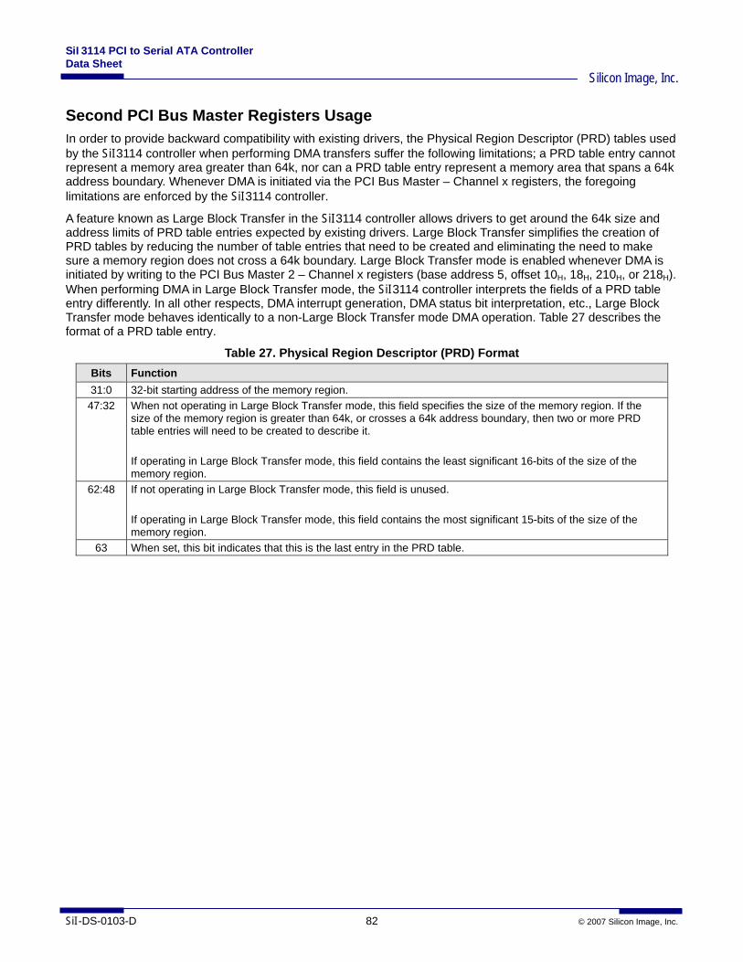
SiI3114 PCI to Serial ATA Controller Data Sheet
Silicon Image, Inc.
SiI-DS-0103-D 82 © 2007 Silicon Image, Inc.
Second PCI Bus Master Registers Usage In order to provide backward compatibility with existing drivers, the Physical Region Descriptor (PRD) tables used by the SiI3114 controller when performing DMA transfers suffer the following limitations; a PRD table entry cannot represent a memory area greater than 64k, nor can a PRD table entry represent a memory area that spans a 64k address boundary. Whenever DMA is initiated via the PCI Bus Master – Channel x registers, the foregoing limitations are enforced by the SiI3114 controller.
A feature known as Large Block Transfer in the SiI3114 controller allows drivers to get around the 64k size and address limits of PRD table entries expected by existing drivers. Large Block Transfer simplifies the creation of PRD tables by reducing the number of table entries that need to be created and eliminating the need to make sure a memory region does not cross a 64k boundary. Large Block Transfer mode is enabled whenever DMA is initiated by writing to the PCI Bus Master 2 – Channel x registers (base address 5, offset 10H, 18H, 210H, or 218H). When performing DMA in Large Block Transfer mode, the SiI3114 controller interprets the fields of a PRD table entry differently. In all other respects, DMA interrupt generation, DMA status bit interpretation, etc., Large Block Transfer mode behaves identically to a non-Large Block Transfer mode DMA operation. Table 27 describes the format of a PRD table entry.
Table 27. Physical Region Descriptor (PRD) Format Bits Function 31:0 32-bit starting address of the memory region.
47:32 When not operating in Large Block Transfer mode, this field specifies the size of the memory region. If the size of the memory region is greater than 64k, or crosses a 64k address boundary, then two or more PRD table entries will need to be created to describe it. If operating in Large Block Transfer mode, this field contains the least significant 16-bits of the size of the memory region.
62:48 If not operating in Large Block Transfer mode, this field is unused. If operating in Large Block Transfer mode, this field contains the most significant 15-bits of the size of the memory region.
63 When set, this bit indicates that this is the last entry in the PRD table.

SiI3114 PCI to Serial ATA Controller Data Sheet
Silicon Image, Inc.
© 2007 Silicon Image, Inc. 83 SiI-DS-0103-D
Power Management Power Management in the SiI3114 is controlled by the register bits described in Table 28.
Table 28. Power Management Register Bits Register Bits Description SMisc PMCHG
Bit 6 This bit reports a change in the Power Management mode. It corresponds to the interrupt enabled by bit 26 of SIEN.
SMisc PMMODE Bits 5,4
These bits report the power management mode status: bit 5 corresponds to Slumber mode; bit 4 to Partial mode. A transition on either of these bits causes a Power Management mode change interrupt.
SError W Bit 18
ComWake received from the Serial ATA bus
SMisc ComWake Bit 11
Generates a ComWake condition on the Serial ATA bus
SMisc PMREQ Bits 1,0
Generates a request from the Host for the Device to go to a Power Management state; bit 1 corresponds to Slumber mode; bit 0 corresponds to Partial mode. These bits are effective regardless of the state of the HPMDS bit.
SControl IPM Bits 11-8
This bit field disables transitions to Partial or Slumber power management states; bit 9 corresponds to Slumber mode; bit 8 corresponds to Partial mode.
SStatus IPM Bits 11-8
This bit field reports the power management state; ‘0110’ corresponds to Slumber mode; ‘0010’ corresponds to Partial mode.
Power Management Summary There are two power management modes: Partial and Slumber. These power management modes may be software initiated through the SMisc register or device initiated from the Serial ATA device.
Transitions to and from either power management mode generate an interrupt, the Power Management Mode Change Interrupt, which may be masked in the SMisc register (bit 26).
Partial Power Management Mode Partial mode may be initiated by software through the SMisc register (bit 0). By setting the bit, the software causes PMREQ_P primitives (Power Management REQuest – Partial) to be sent to the Serial ATA device, which will respond with either a PMACK or PMNAK. If a PMACK is received the Partial mode is entered; A PMNAK is ignored; the request remains asserted.
The Serial ATA device may initiate partial mode. This is indicated by the reception of PMREQ_P primitives from the device. Software enables the acknowledgement of this request by setting the IPM value in the SControl register to ‘00x1’ If enabled, a PMACK will be sent to the device; if not enabled, a PMNAK will be sent. When the request is received and its acknowledgement is enabled, Partial mode is entered.
Partial mode status is reported in both the SStatus register (‘0010’ in the IPM field) and the SMisc register (bit 4).
Partial mode is cleared by setting the ComWake bit in the Smisc register. This will send a COMWAKE signal to the device through the Serial ATA link to initiate a Partial to On sequence. Partial mode can also be cleared through receipt of OOB signals from the device.
Slumber Power Management Mode Slumber mode may be initiated by software through the SMisc register (bit 1). By setting the bit, software causes PMREQ_S primitives to be sent to the Serial ATA device, which will respond with either a PMACK or PMNAK. If a PMACK is received the Slumber mode is entered. A PMNAK is ignored; the request remains asserted.
The Serial ATA device may initiate slumber mode. This is indicated by the reception of PMREQ_S primitives. Software enables the acknowledgement of this request by setting the IPM value in the SControl register to ‘001x’.
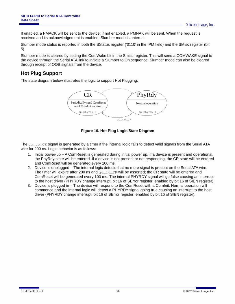
SiI3114 PCI to Serial ATA Controller Data Sheet
Silicon Image, Inc.
SiI-DS-0103-D 84 © 2007 Silicon Image, Inc.
If enabled, a PMACK will be sent to the device; if not enabled, a PMNAK will be sent. When the request is received and its acknowledgement is enabled, Slumber mode is entered.
Slumber mode status is reported in both the SStatus register (‘0110’ in the IPM field) and the SMisc register (bit 5).
Slumber mode is cleared by setting the ComWake bit in the Smisc register. This will send a COMWAKE signal to the device through the Serial ATA link to initiate a Slumber to On sequence. Slumber mode can also be cleared through receipt of OOB signals from the device.
Hot Plug Support The state diagram below illustrates the logic to support Hot Plugging.
CR PhyRdyPeriodically send ComReset
until ComInit received Normal operation
go_to_CR
dp_phyrdy=0 dp_phyrdy=1
Figure 10. Hot Plug Logic State Diagram
The go_to_CR signal is generated by a timer if the internal logic fails to detect valid signals from the Serial ATA wire for 200 ns. Logic behavior is as follows:
1. Initial power-up – A ComReset is generated during initial power up. If a device is present and operational, the PhyRdy state will be entered. If a device is not present or not responding, the CR state will be entered and ComReset will be generated every 100 ms.
2. Device is unplugged – The internal logic detects that no more signal is present on the Serial ATA wire. The timer will expire after 200 ns and go_to_CR will be asserted; the CR state will be entered and ComReset will be generated every 100 ms. The internal PHYRDY signal will go false causing an interrupt to the host driver (PHYRDY change interrupt, bit 16 of SError register; enabled by bit 16 of SIEN register).
3. Device is plugged in – The device will respond to the ComReset with a ComInit. Normal operation will commence and the internal logic will detect a PHYRDY signal going true causing an interrupt to the host driver (PHYRDY change interrupt, bit 16 of SError register; enabled by bit 16 of SIEN register).
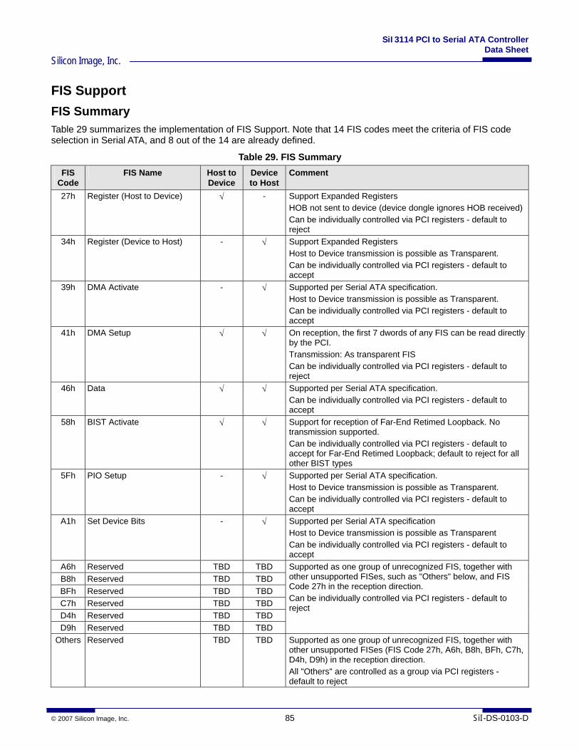
SiI3114 PCI to Serial ATA Controller Data Sheet
Silicon Image, Inc.
© 2007 Silicon Image, Inc. 85 SiI-DS-0103-D
FIS Support FIS Summary Table 29 summarizes the implementation of FIS Support. Note that 14 FIS codes meet the criteria of FIS code selection in Serial ATA, and 8 out of the 14 are already defined.
Table 29. FIS Summary FIS
Code FIS Name Host to
Device Device to Host
Comment
27h Register (Host to Device) √ - Support Expanded Registers HOB not sent to device (device dongle ignores HOB received) Can be individually controlled via PCI registers - default to reject
34h Register (Device to Host) - √ Support Expanded Registers Host to Device transmission is possible as Transparent. Can be individually controlled via PCI registers - default to accept
39h DMA Activate - √ Supported per Serial ATA specification. Host to Device transmission is possible as Transparent. Can be individually controlled via PCI registers - default to accept
41h DMA Setup √ √ On reception, the first 7 dwords of any FIS can be read directly by the PCI. Transmission: As transparent FIS Can be individually controlled via PCI registers - default to reject
46h Data √ √ Supported per Serial ATA specification. Can be individually controlled via PCI registers - default to accept
58h BIST Activate √ √ Support for reception of Far-End Retimed Loopback. No transmission supported. Can be individually controlled via PCI registers - default to accept for Far-End Retimed Loopback; default to reject for all other BIST types
5Fh PIO Setup - √ Supported per Serial ATA specification. Host to Device transmission is possible as Transparent. Can be individually controlled via PCI registers - default to accept
A1h Set Device Bits - √ Supported per Serial ATA specification Host to Device transmission is possible as Transparent Can be individually controlled via PCI registers - default to accept
A6h Reserved TBD TBD B8h Reserved TBD TBD BFh Reserved TBD TBD C7h Reserved TBD TBD D4h Reserved TBD TBD D9h Reserved TBD TBD
Supported as one group of unrecognized FIS, together with other unsupported FISes, such as "Others" below, and FIS Code 27h in the reception direction. Can be individually controlled via PCI registers - default to reject
Others Reserved TBD TBD Supported as one group of unrecognized FIS, together with other unsupported FISes (FIS Code 27h, A6h, B8h, BFh, C7h, D4h, D9h) in the reception direction. All "Others" are controlled as a group via PCI registers - default to reject
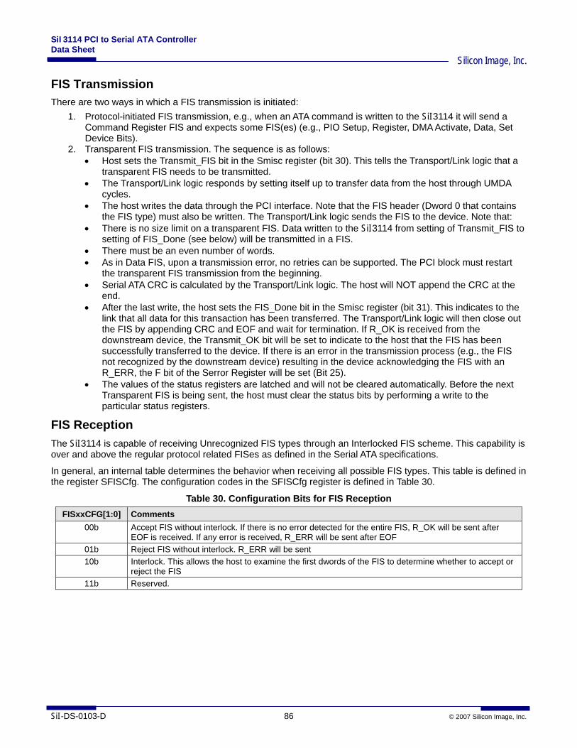
SiI3114 PCI to Serial ATA Controller Data Sheet
Silicon Image, Inc.
SiI-DS-0103-D 86 © 2007 Silicon Image, Inc.
FIS Transmission There are two ways in which a FIS transmission is initiated:
1. Protocol-initiated FIS transmission, e.g., when an ATA command is written to the SiI3114 it will send a Command Register FIS and expects some FIS(es) (e.g., PIO Setup, Register, DMA Activate, Data, Set Device Bits).
2. Transparent FIS transmission. The sequence is as follows: • Host sets the Transmit_FIS bit in the Smisc register (bit 30). This tells the Transport/Link logic that a
transparent FIS needs to be transmitted. • The Transport/Link logic responds by setting itself up to transfer data from the host through UMDA
cycles. • The host writes the data through the PCI interface. Note that the FIS header (Dword 0 that contains
the FIS type) must also be written. The Transport/Link logic sends the FIS to the device. Note that: • There is no size limit on a transparent FIS. Data written to the SiI3114 from setting of Transmit_FIS to
setting of FIS_Done (see below) will be transmitted in a FIS. • There must be an even number of words. • As in Data FIS, upon a transmission error, no retries can be supported. The PCI block must restart
the transparent FIS transmission from the beginning. • Serial ATA CRC is calculated by the Transport/Link logic. The host will NOT append the CRC at the
end. • After the last write, the host sets the FIS_Done bit in the Smisc register (bit 31). This indicates to the
link that all data for this transaction has been transferred. The Transport/Link logic will then close out the FIS by appending CRC and EOF and wait for termination. If R_OK is received from the downstream device, the Transmit_OK bit will be set to indicate to the host that the FIS has been successfully transferred to the device. If there is an error in the transmission process (e.g., the FIS not recognized by the downstream device) resulting in the device acknowledging the FIS with an R_ERR, the F bit of the Serror Register will be set (Bit 25).
• The values of the status registers are latched and will not be cleared automatically. Before the next Transparent FIS is being sent, the host must clear the status bits by performing a write to the particular status registers.
FIS Reception The SiI3114 is capable of receiving Unrecognized FIS types through an Interlocked FIS scheme. This capability is over and above the regular protocol related FISes as defined in the Serial ATA specifications.
In general, an internal table determines the behavior when receiving all possible FIS types. This table is defined in the register SFISCfg. The configuration codes in the SFISCfg register is defined in Table 30.
Table 30. Configuration Bits for FIS Reception FISxxCFG[1:0] Comments
00b Accept FIS without interlock. If there is no error detected for the entire FIS, R_OK will be sent after EOF is received. If any error is received, R_ERR will be sent after EOF
01b Reject FIS without interlock. R_ERR will be sent 10b Interlock. This allows the host to examine the first dwords of the FIS to determine whether to accept or
reject the FIS 11b Reserved.
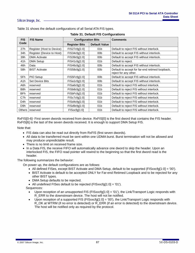
SiI3114 PCI to Serial ATA Controller Data Sheet
Silicon Image, Inc.
© 2007 Silicon Image, Inc. 87 SiI-DS-0103-D
Table 31 shows the default configurations of all Serial ATA FIS types.
Table 31. Default FIS Configurations Configuration Bits FIS
Code FIS Name
Register Bits Default Value Comments
27h Register (Host to Device) FIS27cfg[1:0] 01b Default to reject FIS without interlock. 34h Register (Device to Host) FIS34cfg[1:0] 00b Default to accept FIS without interlock. 39h DMA Activate FIS39cfg[1:0] 00b Default to accept FIS without interlock. 41h DMA Setup FIS41cfg[1:0] 01b Default to reject. 46h Data FIS46cfg[1:0] 00b Default to accept FIS without interlock. 58h BIST Activate FIS58cfg[1:0] 00b Default to accept for far-end retimed loopback,
reject for any other. 5Fh PIO Setup FIS5Fcfg[1:0] 00b Default to accept FIS without interlock. A1h Set Device Bits FISa1cfg[1:0] 00b Default to accept FIS without interlock. A6h reserved FISa6cfg[1:0] 01b Default to reject FIS without interlock. B8h reserved FISb8cfg[1:0] 01b Default to reject FIS without interlock. BFh reserved FISbFcfg[1:0] 01b Default to reject FIS without interlock. C7h reserved FISc7cfg[1:0] 01b Default to reject FIS without interlock. D4h reserved FISd4cfg[1:0] 01b Default to reject FIS without interlock. D9h reserved FISd9cfg[1:0] 01b Default to reject FIS without interlock.
Others reserved FISocfg[1:0] 01b Default to reject FIS without interlock. RxFIS[0-6]- First seven dwords received from device. RxFIS[0] is the first dword that contains the FIS header. RxFIS[6] is the last of the seven dwords received. It is enough to support DMA Setup FIS.
Note that: • FIS data can also be read out directly from RxFIS (first seven dwords). • All data to be transferred must be sent within one UDMA burst. Burst termination will not be allowed and
may produce unpredictable result. • There is no limit on received frame size. • In a Data FIS, the receive FIFO will automatically advance one dword to skip the header. Upon an
interlocked FIS, the FIFO read pointer will rewind to the beginning so that the first dword read is the header.
The following summarizes the behavior: On power up, the default configurations are as follows:
• All defined FISes, except BIST Activate and DMA Setup, default to be supported (FISxxcfg[1:0] = '00'). • BIST Activate is default to be accepted ONLY for Far-end Retimed Loopback and to be rejected for any
other BIST types. • DMA Setup defaults to be rejected. • All undefined FISes default to be rejected (FISxxcfg[1:0] = '01').
Sequences: • Upon reception of an unsupported FIS (FISxxcfg[1:0] = '01'), the Link/Transport Logic responds with
R_ERR to the downstream device. The host will not be notified. • Upon reception of a supported FIS (FISxxcfg[1:0] = '00'), the Link/Transport Logic responds with
R_OK at WTRM (if no error is detected) or R_ERR (if an error is detected) to the downstream device. The host will be notified only as required by the protocol.
SiI3114 PCI to Serial ATA Controller Data Sheet
Silicon Image, Inc.
SiI-DS-0103-D 88 © 2007 Silicon Image, Inc.
• Upon reception of an interlocked FIS (FISxxcfg[1:0] = '10'), the Link/Transport Logic sets the IntrlckFIS bit in the Smisc register. The following describes the possible sequence of events:
Sequence 1: The Link Logic will continue to receive data while its buffer is being filled up.
IntrlckFIS will cause an interrupt to the host. The first 7 Dwords of the FIS are available to the host in the RxFIS0 to RxFIS6
registers.The driver will check the FIS type, clean up the PCI section, arm the DMA controller, and then assert the Rx_IFIS bit in the Smisc register.
The Link/Transport Logic transfers the received FIS, including the header, through the PCI interface to the host.
When all the data is received with no errors, the Link/Transport Logic will assert the IFIS_OK bit in the Smisc register. Otherwise one of the error bits will be set in the Serror register.
The host will set the Accept_IFIS bit to accept or Reject_IFIS to reject the FIS. If no error is detected inside the frame and the Accept_IFIS bit is asserted, the
Link/Transport Logic will send R_OK to the downstream device. If Reject_IFIS is asserted or any error is detected, the Link/Transport Logic will respond with R_ERR. Note that there is an interlock - if the frame is good, it will always wait for the Accept_IFIS or Reject_IFIS (if not asserted already) before responding.
Sequence 2: Link/Transport Logic will continue to receive data while its buffer is being filled up.
IntrlckFIS will cause an interrupt to the host. Host reads the header; the driver will check the FIS type in RxFIS register and
knows that the entire FIS is not larger than the size of RxFIS0 to 6 register. Host waits for IFIS_OK (if any error detected – the error signals). If IFIS_OK is received, host reads all data directly via PCI registers and then issues
an Accept_IFIS (Link/Transport Logic to send R_OK) or a Reject_IFIS (Link/Transport Logic to send R_ERR).
If any error is detected, host can ignore, the Link will respond with R_ERR anyway.
SiI3114 PCI to Serial ATA Controller Data Sheet
Silicon Image, Inc.
© 2007 Silicon Image, Inc. 89 SiI-DS-0103-D
FIS Types Not Affiliated with Current ATA/ATAPI Operations BIST Support Far-End Retimed Loopback is supported in reception mode only. All other BIST codes will be rejected via R_ERR. It defaults to be interlocked supported (for Far-End Retimed Loopback only).
The SiI3114 does not support any BIST in transmission mode. There is no provision to send the test patterns and compare against loopback data.
BIST Signals When SiI3114 enters the BIST operation, the “PHY offline” mode will be set in the DET bits of the Sstatus register. This conditoin will remain asserted until the host generates an ATA reset (hreset_b asserted) or a COMINIT is received from the device.
DMA Setup DMA Setup FIS can only be sent as a transparent FIS. On Power up, DMA Setup FIS defaults to be rejected.
First Party DMA Read of Host Memory by Device Sequence (FIS41cfg[1:0] = '10', i.e. interlocked): Device sends DMA Setup FIS to host. The "D" field in the FIS is '0'. The IntrlckFIS bit is set and causes an interrupt to the host. The host driver checks the FIS type (RxFIS), sets up, and arms the DMA controller. The host sets the DMAOutEn in the Serial ATA SMisc register. The host sets the FPDMAWr in the Serial ATA SMisc register. The host sets the Accept_FIS bit to accept the FIS. The host sends one or more Data FISes. Note that no DMA Activate FIS is required for first party DMA. There is no need to report transfer status. The host clears the DMAOutEn when the transfer count is exhausted.
First Party DMA Write of Host Memory by Device Sequence (FIS41cfg[1:0] = '10', i.e. interlocked): Device sends DMA Setup FIS to host. The "D" field in the FIS is '1'. The IntrlckFIS bit is set and causes an interrupt to the host. The host driver checks the FIS type (RxFIS), sets up, and arms the DMA controller. The host sets the DMAInEn in the Serial ATA SMisc register. The host sets the Accept_FIS bit to accept the FIS. The device sends one or more Data FISes. There is no need to report transfer status. The host clears the DMAInEn when the transfer count is exhausted
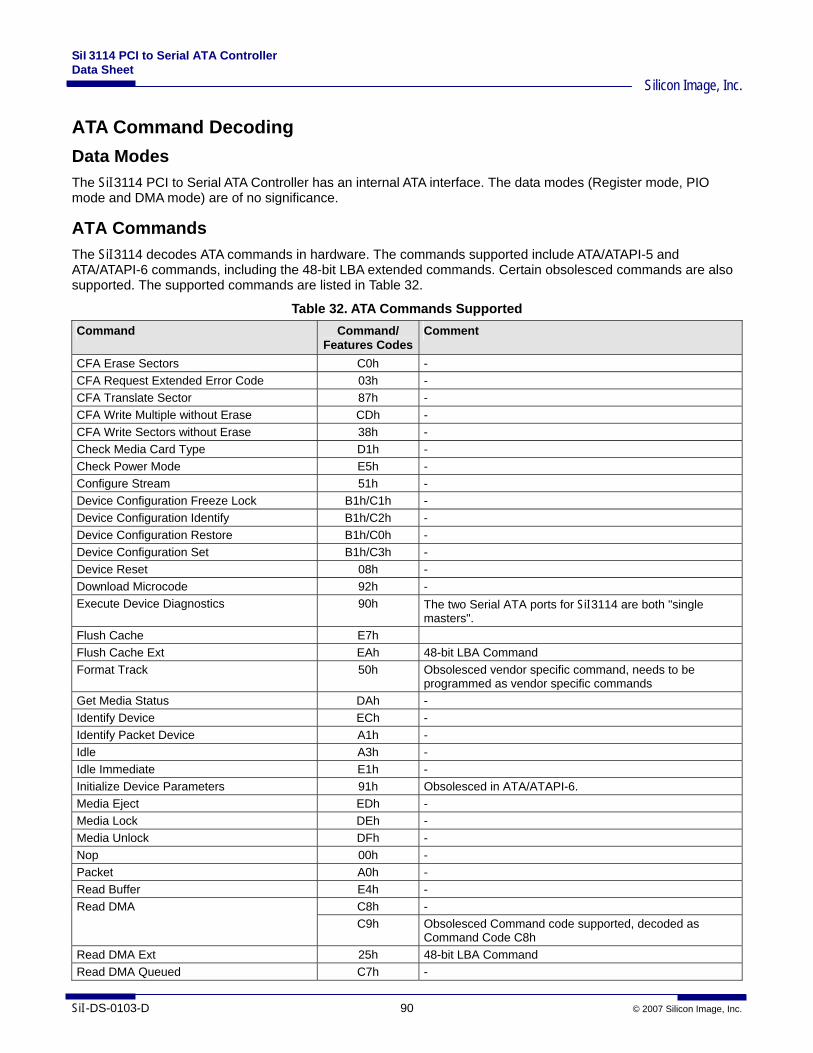
SiI3114 PCI to Serial ATA Controller Data Sheet
Silicon Image, Inc.
SiI-DS-0103-D 90 © 2007 Silicon Image, Inc.
ATA Command Decoding Data Modes The SiI3114 PCI to Serial ATA Controller has an internal ATA interface. The data modes (Register mode, PIO mode and DMA mode) are of no significance.
ATA Commands The SiI3114 decodes ATA commands in hardware. The commands supported include ATA/ATAPI-5 and ATA/ATAPI-6 commands, including the 48-bit LBA extended commands. Certain obsolesced commands are also supported. The supported commands are listed in Table 32.
Table 32. ATA Commands Supported Command Command/
Features CodesComment
CFA Erase Sectors C0h - CFA Request Extended Error Code 03h - CFA Translate Sector 87h - CFA Write Multiple without Erase CDh - CFA Write Sectors without Erase 38h - Check Media Card Type D1h - Check Power Mode E5h - Configure Stream 51h - Device Configuration Freeze Lock B1h/C1h - Device Configuration Identify B1h/C2h - Device Configuration Restore B1h/C0h - Device Configuration Set B1h/C3h - Device Reset 08h - Download Microcode 92h - Execute Device Diagnostics 90h The two Serial ATA ports for SiI3114 are both "single
masters". Flush Cache E7h Flush Cache Ext EAh 48-bit LBA Command Format Track 50h Obsolesced vendor specific command, needs to be
programmed as vendor specific commands Get Media Status DAh - Identify Device ECh - Identify Packet Device A1h - Idle A3h - Idle Immediate E1h - Initialize Device Parameters 91h Obsolesced in ATA/ATAPI-6. Media Eject EDh - Media Lock DEh - Media Unlock DFh - Nop 00h - Packet A0h - Read Buffer E4h -
C8h - Read DMA C9h Obsolesced Command code supported, decoded as
Command Code C8h Read DMA Ext 25h 48-bit LBA Command Read DMA Queued C7h -
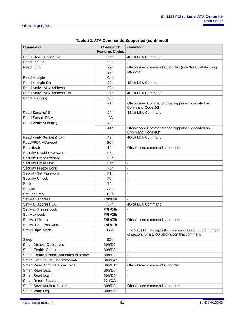
SiI3114 PCI to Serial ATA Controller Data Sheet
Silicon Image, Inc.
© 2007 Silicon Image, Inc. 91 SiI-DS-0103-D
Table 32. ATA Commands Supported (continued)
Command Command/ Features Codes
Comment
Read DMA Queued Ext 26h 48-bit LBA Command Read Log Ext 2Fh -
22h Read Long 23h
Obsolesced command supported (see “Read/Write Long” section)
Read Multiple C4h - Read Multiple Ext 29h 48-bit LBA Command Read Native Max Address F8h - Read Native Max Address Ext 27h 48-bit LBA Command
20h - Read Sector(s) 21h Obsolesced Command code supported, decoded as
Command Code 20h Read Sector(s) Ext 24h 48-bit LBA Command Read Stream DMA 2A -
40h - Read Verify Sector(s) 41h Obsolesced Command code supported, decoded as
Command Code 40h Read Verify Sector(s) Ext 42h 48-bit LBA Command ReadFPDMAQueued 2Ch - Recalibrate 10h Obsolesced command supported. Security Disable Password F6h - Security Erase Prepare F3h - Security Erase Unit F4h - Security Freeze Lock F5h - Security Set Password F1h - Security Unlock F2h - Seek 70h - Service A2h - Set Features EFh - Set Max Address F9h/00h - Set Max Address Ext 37h 48-bit LBA Command Set Max Freeze Lock F9h/04h - Set Max Lock F9h/02h - Set Max Unlock F9h/03h Obsolesced command supported. Set Max Set Password F9h/01h Set Multiple Mode C6h The SiI3114 intercepts the command to set up the number
of sectors for a DRQ block upon this command. Sleep E6h - Smart Disable Operations B0h/D9h - Smart Enable Operations B0h/D8h - Smart Enable/Disable Attributes Autosave B0h/D2h - Smart Execute Off-Line Immediate B0h/D4h - Smart Read Attribute Thresholds B0h/D1h Obsolesced command supported. Smart Read Data B0h/D0h - Smart Read Log B0h/D5h - Smart Return Status B0h/DAh - Smart Save Attribute Values B0h/D3h Obsolesced command supported. Smart Write Log B0h/D6h -
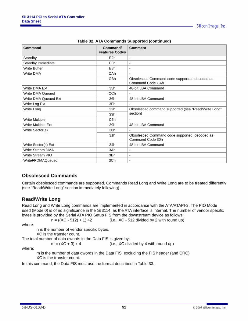
SiI3114 PCI to Serial ATA Controller Data Sheet
Silicon Image, Inc.
SiI-DS-0103-D 92 © 2007 Silicon Image, Inc.
Table 32. ATA Commands Supported (continued)
Command Command/ Features Codes
Comment
Standby E2h - Standby Immediate E0h - Write Buffer E8h -
CAh - Write DMA CBh Obsolesced Command code supported, decoded as
Command Code CAh Write DMA Ext 35h 48-bit LBA Command Write DMA Queued CCh - Write DMA Queued Ext 36h 48-bit LBA Command Write Log Ext 3Fh -
32h Write Long 33h
Obsolesced command supported (see “Read/Write Long” section)
Write Multiple C5h - Write Multiple Ext 39h 48-bit LBA Command
30h - Write Sector(s) 31h Obsolesced Command code supported, decoded as
Command Code 30h Write Sector(s) Ext 34h 48-bit LBA Command Write Stream DMA 3Ah - Write Stream PIO 3Bh - WriteFPDMAQueued 3Ch -
Obsolesced Commands Certain obsolesced commands are supported. Commands Read Long and Write Long are to be treated differently (see “Read/Write Long” section immediately following).
Read/Write Long Read Long and Write Long commands are implemented in accordance with the ATA/ATAPI-3. The PIO Mode used (Mode 0) is of no significance in the SiI3114, as the ATA interface is internal. The number of vendor specific bytes is provided by the Serial ATA PIO Setup FIS from the downstream device as follows: n = ((XC - 512) + 1) ÷2 (i.e., XC - 512 divided by 2 with round up) where:
n is the number of vendor specific bytes. XC is the transfer count.
The total number of data dwords in the Data FIS is given by: m = (XC + 3) ÷ 4 (i.e., XC divided by 4 with round up) where:
m is the number of data dwords in the Data FIS, excluding the FIS header (and CRC). XC is the transfer count.
In this command, the Data FIS must use the format described in Table 33.
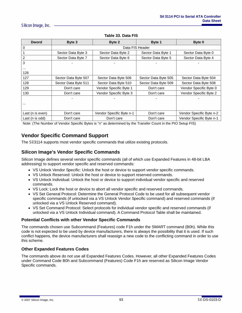
SiI3114 PCI to Serial ATA Controller Data Sheet
Silicon Image, Inc.
© 2007 Silicon Image, Inc. 93 SiI-DS-0103-D
Table 33. Data FIS Dword Byte 3 Byte 2 Byte 1 Byte 0
0 Data FIS Header 1 Sector Data Byte 3 Sector Data Byte 2 Sector Data Byte 1 Sector Data Byte 0 2 Sector Data Byte 7 Sector Data Byte 6 Sector Data Byte 5 Sector Data Byte 4 3 ... 126
- - - -
127 Sector Data Byte 507 Sector Data Byte 506 Sector Data Byte 505 Sector Data Byte 504 128 Sector Data Byte 511 Sector Data Byte 510 Sector Data Byte 509 Sector Data Byte 508 129 Don't care Vendor Specific Byte 1 Don't care Vendor Specific Byte 0 130 Don't care Vendor Specific Byte 3 Don't care Vendor Specific Byte 2 ...
- - - -
Last (n is even) Don't care Vendor Specific Byte n-1 Don't care Vendor Specific Byte n-2 Last (n is odd) Don't care Don't care Don't care Vendor Specific Byte n-1 Note: (The Number of Vendor Specific Bytes is "n" as determined by the Transfer Count in the PIO Setup FIS)
Vendor Specific Command Support The SiI3114 supports most vendor specific commands that utilize existing protocols.
Silicon Image's Vendor Specific Commands Silicon Image defines several vendor specific commands (all of which use Expanded Features in 48-bit LBA addressing) to support vendor specific and reserved commands:
• VS Unlock Vendor Specific: Unlock the host or device to support vendor specific commands. • VS Unlock Reserved: Unlock the host or device to support reserved commands. • VS Unlock Individual: Unlock the host or device to support individual vendor specific and reserved
commands. • VS Lock: Lock the host or device to abort all vendor specific and reserved commands. • VS Set General Protocol: Determine the General Protocol Code to be used for all subsequent vendor
specific commands (if unlocked via a VS Unlock Vendor Specific command) and reserved commands (if unlocked via a VS Unlock Reserved command).
• VS Set Command Protocol: Select protocols for individual vendor specific and reserved commands (if unlocked via a VS Unlock Individual command). A Command Protocol Table shall be maintained.
Potential Conflicts with other Vendor Specific Commands The commands chosen use Subcommand (Features) code F1h under the SMART command (B0h). While this code is not expected to be used by device manufacturers, there is always the possibility that it is used. If such conflict happens, the device manufacturers shall reassign a new code to the conflicting command in order to use this scheme.
Other Expanded Features Codes The commands above do not use all Expanded Features Codes. However, all other Expanded Features Codes under Command Code B0h and Subcommand (Features) Code F1h are reserved as Silicon Image Vendor Specific commands.
SiI3114 PCI to Serial ATA Controller Data Sheet
Silicon Image, Inc.
SiI-DS-0103-D 94 © 2007 Silicon Image, Inc.
Vendor Specific, Reserved, Retired and Obsolesced Commands These types of commands are treated differently:
• Vendor specific commands: Expect for those commands whose protocols are individually set (via the VS Unlock Individual and VS Set Command Protocol commands), the host or device must be unlocked via the VS Unlock Vendor Specific command before such commands can be issued. Otherwise, vendor specific commands are aborted.
• Reserved commands: Expect for those commands whose protocols are individually set (via the VS Set Unlock Individual and VS Set Command Protocol commands), the host or device must be unlocked via the VS Unlock Reserved command before such commands can be issued. Otherwise, reserved commands are aborted.
• Obsolesced and Retired commands: Implementation of such commands is optional.
Definitions • Command - Unless otherwise stated, this is the value written to the ATA Command Register. • Command Code - This is the code corresponding to the ATA command. It is also a field in the Command
Protocol Table. • Command Protocol Table - The table that contains the individual vendor specific and reserved commands
supported (see on page 108). • Features - Unless otherwise stated, this is the value written to the ATA Features Register. • Features Code - This is the code corresponding to the ATA Features register. It is also a field in the
Command Protocol Table. • Features Mask - This is a field in the Command Protocol Table that allows several Features Codes to be
used for the same command. • General Protocol Code - On a VS Set General Protocol command after a VS Unlock Vendor Specific or VS
Unlock Reserved command, the General Protocol Code shall be set as the protocol for all undefined vendor specific (if unlocked) and/or undefined reserved (if unlocked) commands. An undefined vendor specific/reserved command is one that does not have an entry in the Command Protocol Table.
• Protocol Code - This code determines the protocol associate with a command. It is also a field in the Command Protocol Table.
• Subcommand Code - Same as Features Code. • VS Features Set - The commands needed to support this scheme (See “Bridge Device Vendor Specific
Commands” section on page 96 for more details.). • VS State Machine - The state machine that determines what vendor specific and reserved commands are
to be supported (See “State Transitions” section on page 109 for more details.).
Scheme Reset Upon any hardware reset or the Serial ATA COMRESET, or COMINIT, the VS State Machine shall be initialized to the locked state (the "default" state), which shall abort all vendor specific and reserved commands. Soft Reset (via Device Control register bit 2) shall NOT affect the VS State Machine.
SiI3114 PCI to Serial ATA Controller Data Sheet
Silicon Image, Inc.
© 2007 Silicon Image, Inc. 95 SiI-DS-0103-D
Operation The following summarizes how the vendor specific/reserved commands are supported. Detailed operations are described in later sections.
The default state is locked. All vendor specific commands shall be aborted. Unlock:
• To unlock the Serial ATA host or device to support vendor specific commands: Issue a VS Unlock Vendor Specific command. A Serial ATA host supporting the VS scheme will also send this command to the Serial ATA device. If the downstream Serial ATA device is a bridge, the device bridge may optionally issue this command to the attached parallel ATA device. Note that the unlock will take effect in the Serial ATA host and the Serial ATA device even if an ABORT status is reported.
• To unlock the Serial ATA host or device to support reserved commands: Issue a VS Unlock Reserved command. A Serial ATA host supporting the VS scheme will also send this command to the Serial ATA device. If the downstream Serial ATA device is a bridge, the device bridge may optionally issue this command to the attached parallel ATA device. Note that the unlock will take effect in the Serial ATA host and the Serial ATA device even if an ABORT status is reported.
• To support individual vendor specific or reserved command: Issue a VS Unlock Individual command. Combinations of the above can be supported by simply issuing the appropriate combinations of VS Unlock Vendor Specific, VS Unlock Reserved and VS Unlock Individual commands.
Set protocol. There are two ways to set up protocol(s): • Issue a VS Set Command Protocol command to set up a protocol for a specific command. The information
is logged in a Command Protocol Table. This protocol shall remain valid until overwritten by a VS Set Command Protocol command that overwrites the Command Protocol Table entry, the VS Lock command, hardware reset, COMRESET, or COMINIT. A Serial ATA host supporting the VS scheme will also send this command to the Serial ATA device. If the downstream Serial ATA device is a bridge, the device bridge may optionally issue this command to the attached parallel ATA device. Note that the protocol shall be set in the Serial ATA host and the Serial ATA device even if an ABORT status is reported. If more than one command protocol has to be set up, a VS Set Command protocol shall be issued for each command.
• Issue a VS Set General Protocol command to set the General Protocol Code for the next vendor specific command. This protocol shall remain valid until the next VS Set General Protocol command, VS Lock command, hardware reset, COMRESET, or COMINIT. A Serial ATA host supporting the VS scheme will also send this command to the Serial ATA device. If the downstream Serial ATA device is a bridge, the device bridge may optionally issue this command to the attached parallel ATA device. Note that the protocol shall be set in the Serial ATA host and the Serial ATA device even if an ABORT status is reported. Commands already set up via the VS Set Command Protocol shall follow the protocol set in the VS Set Command Protocol command instead of the one set in this command.
Issue any commands: • Any vendor specific commands (if unlocked for vendor specific commands) or reserved commands (if
unlocked for reserved commands) that has an associated protocol set via the VS Set Command Protocol command shall be executed using that protocol.
• Any vendor specific commands (if unlocked for vendor specific commands) or reserved commands (if unlocked for reserved commands) that does not have an associated protocol, i.e. not set up by the VS Set Command Protocol command, shall be executed using the protocol loaded from the latest VS Set General Protocol command.
• Other supported commands shall follow the predefined protocols. • Other unsupported commands shall be aborted.
To change the protocol for vendor specific commands, simply reissue the VS Set General Protocol or the VS Set Command Protocol command with the new protocol.
When done, issue the VS Lock command to return to the default VS state. A Serial ATA host supporting the VS scheme will also send the VS Lock command to the Serial ATA device. If the downstream Serial ATA device is a bridge, the device bridge may optionally issue this command to the attached parallel ATA device. Note that the lock will take effect in the Serial ATA host and the Serial ATA device even if an ABORT status is reported.
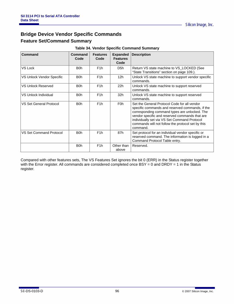
SiI3114 PCI to Serial ATA Controller Data Sheet
Silicon Image, Inc.
SiI-DS-0103-D 96 © 2007 Silicon Image, Inc.
Bridge Device Vendor Specific Commands Feature Set/Command Summary
Table 34. Vendor Specific Command Summary Command Command
Code Features
Code Expanded Features
Code
Description
VS Lock B0h F1h D5h Return VS state machine to VS_LOCKED (See “State Transitions” section on page 109.).
VS Unlock Vendor Specific B0h F1h 12h Unlock VS state machine to support vendor specific commands.
VS Unlock Reserved B0h F1h 22h Unlock VS state machine to support reserved commands.
VS Unlock Individual B0h F1h 32h Unlock VS state machine to support reserved commands.
VS Set General Protocol B0h F1h F0h Set the General Protocol Code for all vendor specific commands and reserved commands, if the corresponding command types are unlocked. The vendor specific and reserved commands that are individually set via VS Set Command Protocol commands will not follow the protocol set by this command.
VS Set Command Protocol B0h F1h 87h Set protocol for an individual vendor specific or reserved command. The information is logged in a Command Protocol Table entry.
B0h F1h Other than above
Reserved.
Compared with other features sets, The VS Features Set ignores the bit 0 (ERR) in the Status register together with the Error register. All commands are considered completed once BSY = 0 and DRDY = 1 in the Status register.
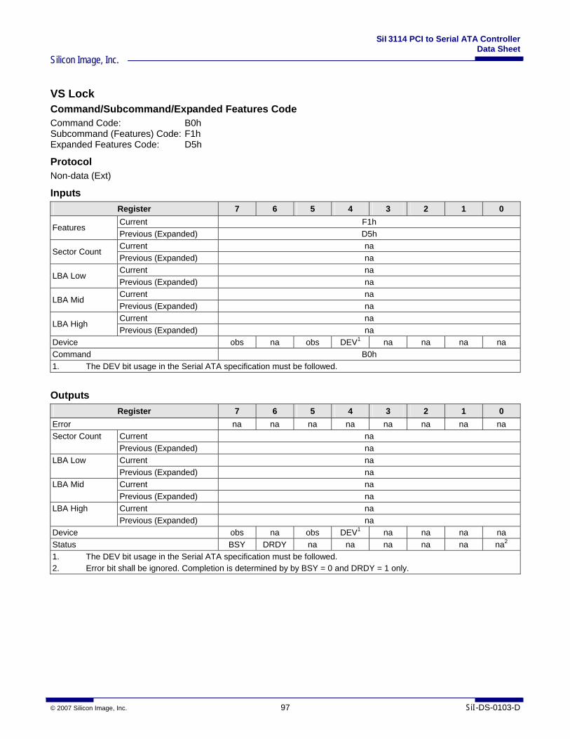
SiI3114 PCI to Serial ATA Controller Data Sheet
Silicon Image, Inc.
© 2007 Silicon Image, Inc. 97 SiI-DS-0103-D
VS Lock Command/Subcommand/Expanded Features Code Command Code: B0h Subcommand (Features) Code: F1h Expanded Features Code: D5h
Protocol Non-data (Ext)
Inputs Register 7 6 5 4 3 2 1 0 Current F1h
Features Previous (Expanded) D5h Current na
Sector Count Previous (Expanded) na Current na
LBA Low Previous (Expanded) na Current na
LBA Mid Previous (Expanded) na Current na
LBA High Previous (Expanded) na
Device obs na obs DEV1 na na na na Command B0h 1. The DEV bit usage in the Serial ATA specification must be followed.
Outputs Register 7 6 5 4 3 2 1 0
Error na na na na na na na na Current na Sector Count Previous (Expanded) na Current na LBA Low Previous (Expanded) na Current na LBA Mid Previous (Expanded) na Current na LBA High Previous (Expanded) na
Device obs na obs DEV1 na na na na Status BSY DRDY na na na na na na2 1. The DEV bit usage in the Serial ATA specification must be followed. 2. Error bit shall be ignored. Completion is determined by by BSY = 0 and DRDY = 1 only.
SiI3114 PCI to Serial ATA Controller Data Sheet
Silicon Image, Inc.
SiI-DS-0103-D 98 © 2007 Silicon Image, Inc.
Feature Set Mandatory for all Serial ATA components supporting the VS feature set.
Description This command locks the host and device bridges from supporting vendor specific commands. All vendor specific and reserved commands issued afterwards will be aborted.
A Serial ATA host, native or bridge, supporting the VS Lock command shall use the non-data (ext) protocol with this command. The Serial ATA host shall send this command to the Serial ATA device. The following situations may happen:
Case 1: The Serial ATA device (native or bridge) responds with a completed status. Both sides are set up to support this scheme.
Case 2: The Serial ATA device bridge supports this scheme. It may optionally pass this command to a parallel ATA device:
• If passed to a parallel ATA device, the parallel ATA device responds with an abort status, which may be reported back to the Serial ATA host.
• If not passed to a parallel ATA device, the device bridge shall still respond with a device-to-host Register FIS to terminate BSY in the Serial ATA host.
However, both the Serial ATA host and the Serial ATA device bridge shall ignore the abort status and shall consider the VS block locked.
The Serial ATA device is a native device and responds with an abort. The Serial ATA host will ignore the abort status and shall consider the VS block locked.
In other words, regardless of the status reported (aborted or complete), the Serial ATA host and device that support this scheme shall be locked.
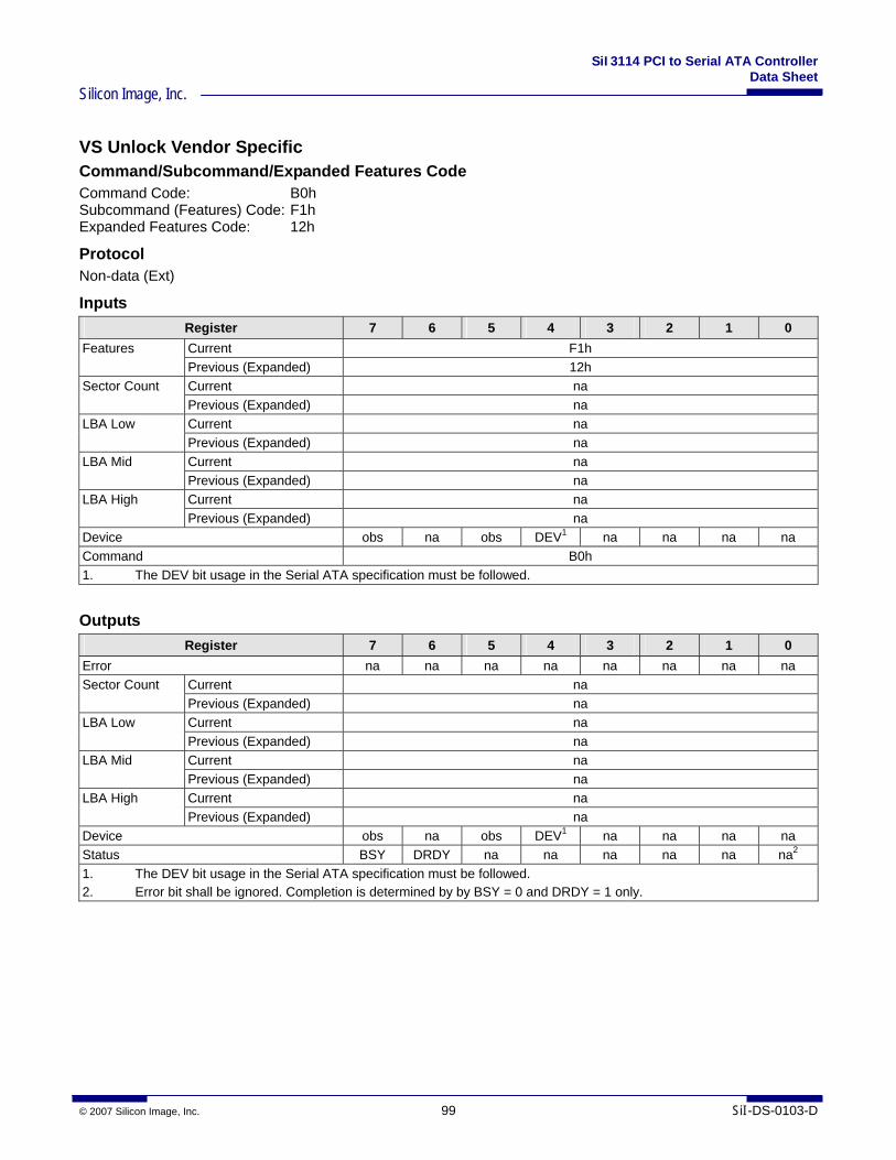
SiI3114 PCI to Serial ATA Controller Data Sheet
Silicon Image, Inc.
© 2007 Silicon Image, Inc. 99 SiI-DS-0103-D
VS Unlock Vendor Specific Command/Subcommand/Expanded Features Code Command Code: B0h Subcommand (Features) Code: F1h Expanded Features Code: 12h
Protocol Non-data (Ext)
Inputs Register 7 6 5 4 3 2 1 0 Current F1h Features Previous (Expanded) 12h Current na Sector Count Previous (Expanded) na Current na LBA Low Previous (Expanded) na Current na LBA Mid Previous (Expanded) na Current na LBA High Previous (Expanded) na
Device obs na obs DEV1 na na na na Command B0h 1. The DEV bit usage in the Serial ATA specification must be followed.
Outputs Register 7 6 5 4 3 2 1 0
Error na na na na na na na na Current na Sector Count Previous (Expanded) na Current na LBA Low Previous (Expanded) na Current na LBA Mid Previous (Expanded) na Current na LBA High Previous (Expanded) na
Device obs na obs DEV1 na na na na Status BSY DRDY na na na na na na2 1. The DEV bit usage in the Serial ATA specification must be followed. 2. Error bit shall be ignored. Completion is determined by by BSY = 0 and DRDY = 1 only.
SiI3114 PCI to Serial ATA Controller Data Sheet
Silicon Image, Inc.
SiI-DS-0103-D 100 © 2007 Silicon Image, Inc.
Feature Set Mandatory for all Serial ATA components supporting the VS feature set.
Description This command unlocks the host and device bridges to support vendor specific commands. Once this command is executed, the bridge(s) shall remain unlocked until:
• A VS Lock command that returns the VS state to the default locked state, or; • A hardware reset, or COMINIT or COMRESET.
Note that the VS Unlock Individual command, the VS Unlock Reserved command and Soft Reset have no effect on the VS state.
If a VS Unlock Individual command is issued afterwards, the bridge(s) shall be unlocked for both individual vendor specific/reserved commands and other vendor specific commands.
If a VS Unlock Reserved command is issued afterwards, the bridge(s) shall be unlocked for both vendor specific and reserved commands.
If both VS Unlock Individual and VS Unlock Reserved are issued afterwards, the bridge(s) shall be unlocked for individual vendor specific/reserved commands, as well as other vendor specific and reserved commands.
A Serial ATA host, native or bridge, supporting the VS Unlock Vendor Specific command shall use the non-data (ext) protocol with this command. The Serial ATA host shall send this command to the Serial ATA device. The following situations may happen:
Case 1: The Serial ATA device (native or bridge) responds with a completed status. Both sides are set up to support this scheme.
Case 2: The Serial ATA device bridge supports this scheme. It may optionally pass this command to a parallel ATA device:
• If passed to a parallel ATA device, the parallel ATA device responds with an abort status, which may be reported back to the Serial ATA host.
• If not passed to a parallel ATA device, the device bridge shall still respond with a device-to-host Register FIS to terminate BSY in the Serial ATA host.
However, both the Serial ATA host and the Serial ATA device bridge shall ignore the abort status and shall consider the unlock event successful.
The Serial ATA device is a native device and responds with an abort. The Serial ATA host will ignore the abort status and shall consider the unlock event successful.
In other words, regardless of the status reported (aborted or complete), the Serial ATA host and device that support this scheme shall be unlocked to support vendor specific commands.

SiI3114 PCI to Serial ATA Controller Data Sheet
Silicon Image, Inc.
© 2007 Silicon Image, Inc. 101 SiI-DS-0103-D
VS Unlock Reserved Command/Subcommand/Expanded Features Code Command Code: B0h Subcommand (Features) Code: F1h Expanded Features Code: 22h
Protocol Non-data (Ext)
Inputs Register 7 6 5 4 3 2 1 0 Current F1h Features Previous (Expanded) 22h Current na Sector Count Previous (Expanded) na Current na LBA Low Previous (Expanded) na Current na LBA Mid Previous (Expanded) na Current na LBA High Previous (Expanded) na
Device obs na obs DEV1 na na na na Command F0h 1. The DEV bit usage in the Serial ATA specification must be followed.
Outputs Register 7 6 5 4 3 2 1 0
Error na na na na na na na na Current na Sector Count Previous (Expanded) na Current na LBA Low Previous (Expanded) na Current na LBA Mid Previous (Expanded) na Current na LBA High Previous (Expanded) na
Device obs na obs DEV1 na na na na Status BSY DRDY na na na na na na2 1. The DEV bit usage in the Serial ATA specification must be followed. 2. Error bit shall be ignored. Completion is determined by by BSY = 0 and DRDY = 1 only.
SiI3114 PCI to Serial ATA Controller Data Sheet
Silicon Image, Inc.
SiI-DS-0103-D 102 © 2007 Silicon Image, Inc.
Feature Set Optional for all Serial ATA components supporting the VS feature set.
Description This command unlocks the host and device bridges to support reserved commands. Once this command is executed, the bridge(s) shall remain unlocked until:
• A VS Lock command that returns the VS state to the default locked state, or; • A hardware reset, or COMINIT or COMRESET.
Note that the VS Unlock Vendor Specific command, the VS Unlock Individual command and Soft Reset have no effect on the VS state.
If a VS Unlock Vendor Specific command is issued afterwards, the bridge(s) shall be unlocked for both reserved and vendor specific commands.
If a VS Unlock Individual command is issued afterwards, the bridge(s) shall be unlocked for both individual vendor specific/reserved command protocols and other reserved commands.
If both VS Unlock Vendor Specific and VS Unlock Individual are issued afterwards, the bridge(s) shall be unlocked for individual vendor specific/reserved command protocols, as well as other vendor specific and reserved commands.
A Serial ATA host, native or bridge, supporting the VS Unlock Reserved command shall use the non-data (ext) protocol with this command. The Serial ATA host shall send this command to the Serial ATA device. The following situations may happen:
Case 1: The Serial ATA device (native or bridge) responds with a completed status. Both sides are set up to support this scheme.
Case 2: The Serial ATA device bridge supports this scheme. It may optionally pass this command to a parallel ATA device:
• If passed to a parallel ATA device, the parallel ATA device responds with an abort status, which may be reported back to the Serial ATA host.
• If not passed to a parallel ATA device, the device bridge shall still respond with a device-to-host Register FIS to terminate BSY in the Serial ATA host.
However, both the Serial ATA host and the Serial ATA device bridge shall ignore the abort status and shall consider the unlock event successful.
The Serial ATA device is a native device and responds with an abort. The Serial ATA host will ignore the abort status and shall consider the unlock event successful.
In other words, regardless of the status reported (aborted or complete), the Serial ATA host and device that support this scheme shall be unlocked to support reserved commands.
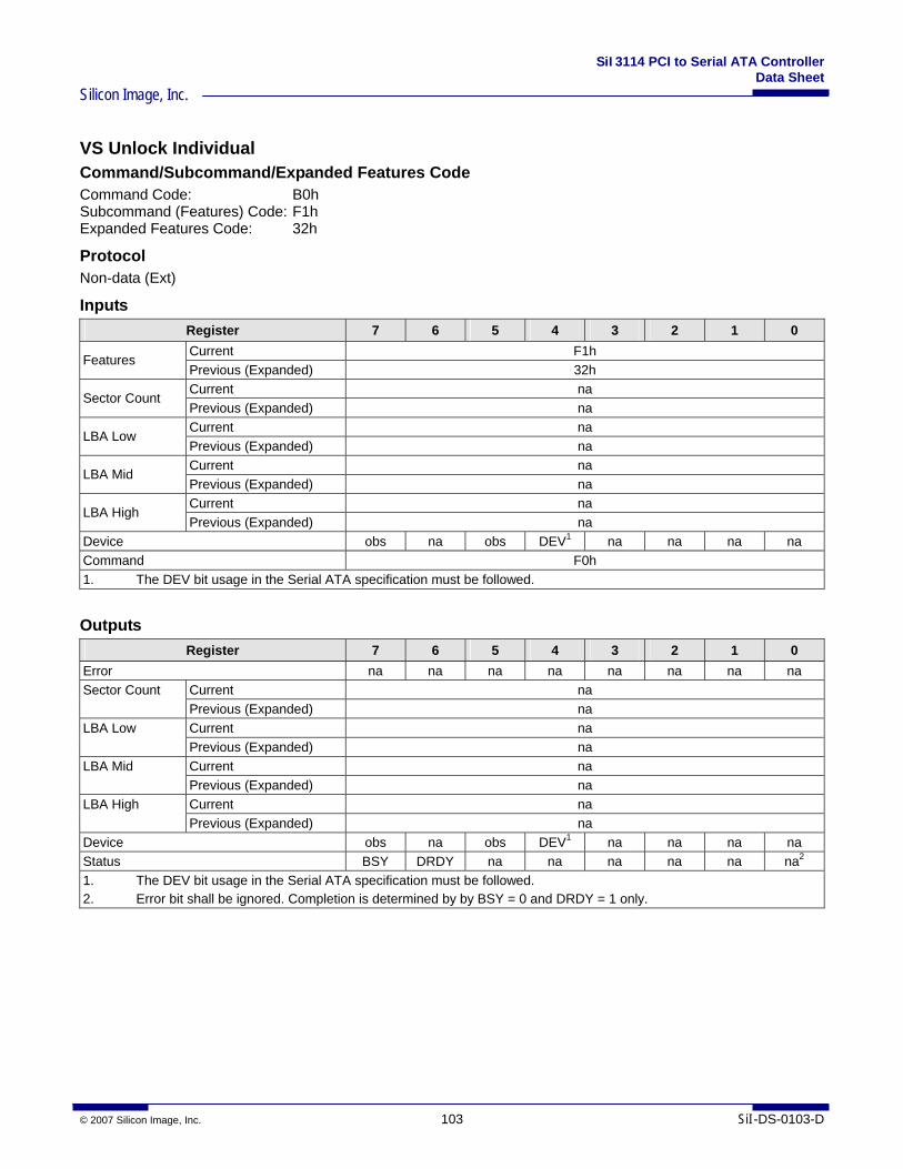
SiI3114 PCI to Serial ATA Controller Data Sheet
Silicon Image, Inc.
© 2007 Silicon Image, Inc. 103 SiI-DS-0103-D
VS Unlock Individual Command/Subcommand/Expanded Features Code Command Code: B0h Subcommand (Features) Code: F1h Expanded Features Code: 32h
Protocol Non-data (Ext)
Inputs Register 7 6 5 4 3 2 1 0 Current F1h
Features Previous (Expanded) 32h Current na
Sector Count Previous (Expanded) na Current na
LBA Low Previous (Expanded) na Current na
LBA Mid Previous (Expanded) na Current na
LBA High Previous (Expanded) na
Device obs na obs DEV1 na na na na Command F0h 1. The DEV bit usage in the Serial ATA specification must be followed.
Outputs Register 7 6 5 4 3 2 1 0
Error na na na na na na na na Current na Sector Count Previous (Expanded) na Current na LBA Low Previous (Expanded) na Current na LBA Mid Previous (Expanded) na Current na LBA High Previous (Expanded) na
Device obs na obs DEV1 na na na na Status BSY DRDY na na na na na na2 1. The DEV bit usage in the Serial ATA specification must be followed. 2. Error bit shall be ignored. Completion is determined by by BSY = 0 and DRDY = 1 only.
SiI3114 PCI to Serial ATA Controller Data Sheet
Silicon Image, Inc.
SiI-DS-0103-D 104 © 2007 Silicon Image, Inc.
Feature Set Optional for all Serial ATA components supporting the VS feature set.
Description This command unlocks the host and device bridges to support individual vendor specific and reserved commands. Once this command is executed, the bridge(s) shall remain unlocked until:
• A VS Lock command that returns the VS state to the default locked state, or; • A hardware reset, or COMINIT or COMRESET.
Note that the VS Unlock Vendor Specific command, the VS Unlock Reserved command and Soft Reset have no effect on the VS state.
If a VS Unlock Vendor Specific command is issued afterwards, the bridge(s) shall be unlocked for both individual command protocols and other vendor specific commands.
If a VS Unlock Reserved command is issued afterwards, the bridge(s) shall be unlocked for both individual vendor specific/reserved command and other reserved commands.
If both VS Unlock Vendor Specific and VS Unlock Reserved are issued afterwards, the bridge(s) shall be unlocked for individual vendor specific/reserved command, as well as other vendor specific and reserved commands.
A Serial ATA host, native or bridge, supporting the VS Unlock Individual command shall use the non-data (ext) protocol with this command. The Serial ATA host shall send this command to the Serial ATA device. The following situations may happen:
Case 1: The Serial ATA device (native or bridge) responds with a completed status. Both sides are set up to support this scheme.
Case 2: The Serial ATA device bridge supports this scheme. It may optionally pass this command to a parallel ATA device:
• If passed to a parallel ATA device, the parallel ATA device responds with an abort status, which may be reported back to the Serial ATA host.
• If not passed to a parallel ATA device, the device bridge shall still respond with a device-to-host Register FIS to terminate BSY in the Serial ATA host.
However, both the Serial ATA host and the Serial ATA device bridge shall ignore the abort status and shall consider the unlock event successful.
The Serial ATA device is a native device and responds with an abort. The Serial ATA host will ignore the abort status and shall consider the unlock event successful.
In other words, regardless of the status reported (aborted or complete), the Serial ATA host and device that support this scheme shall be unlocked to support individual vendor specific/reserved commands.

SiI3114 PCI to Serial ATA Controller Data Sheet
Silicon Image, Inc.
© 2007 Silicon Image, Inc. 105 SiI-DS-0103-D
VS Set General Protocol Command/Subcommand Code/Expanded Features Code Command Code: B0h Subcommand (Features) Code: F1h Expanded Features Code: F0h
Protocol Non-data (Ext)
Inputs Register 7 6 5 4 3 2 1 0 Current F1h Features Previous (Expanded) F0h Current na Sector Count Previous (Expanded) Protocol Code (See “Protocols Summary” section) Current na LBA Low Previous (Expanded) na Current na LBA Mid Previous (Expanded) na Current na LBA High Previous (Expanded) na
Device obs na obs DEV1 na na na na Command B0h 1. The DEV bit usage in the Serial ATA specification must be followed.
Outputs Register 7 6 5 4 3 2 1 0
Error na na na na na na na na Current na
Sector Count Previous (Expanded) na Current na
LBA Low Previous (Expanded) na Current na
LBA Mid Previous (Expanded) na Current na
LBA High Previous (Expanded) na
Device obs na obs DEV1 na na na na Status BSY DRDY na na na na na na2 1. The DEV bit usage in the Serial ATA specification must be followed. 2. Error bit shall be ignored. Completion is determined by by BSY = 0 and DRDY = 1 only.
SiI3114 PCI to Serial ATA Controller Data Sheet
Silicon Image, Inc.
SiI-DS-0103-D 106 © 2007 Silicon Image, Inc.
Feature Set Mandatory for all Serial ATA components supporting the VS feature set.
Description If the VS state is unlocked for vendor specific or for reserved, this command will set the General Protocol Code for the next vendor specific/reserved command(s), except for those individually set via the VS Set Command Protocol commands. The protocol shall be, or return to, Abort (Protocol Code = 00h) upon a lock event, i.e.:
• A VS Lock command to return the VS state to the default locked state, or; • A hardware reset, or COMINIT or COMRESET.
The General Protocol shall be passed to the Serial ATA host and device via the Expanded Sector Count register. The protocols and codes are described in Table 45 through Table 48.
A Serial ATA host, native or bridge, supporting the VS Set General Protocol command shall use the non-data (ext) protocol with this command. The Serial ATA host shall send this command to the Serial ATA device. The following situations may happen:
Case 1: The Serial ATA device (native or bridge) responds with a completed status. Both sides are set up to support this scheme.
Case 2: The Serial ATA device bridge supports this scheme. It may optionally pass this command to a parallel ATA device:
• If passed to a parallel ATA device, the parallel ATA device responds with an abort status, which may be reported back to the Serial ATA host.
• If not passed to a parallel ATA device, the device bridge shall still respond with a device-to-host Register FIS to terminate BSY in the Serial ATA host.
However, both the Serial ATA host and the Serial ATA device bridge shall ignore the abort status and shall consider the protocol set.
The Serial ATA device is a native device and responds with an abort. The Serial ATA host will ignore the abort status and shall consider the protocol set.
In other words, regardless of the status reported (aborted or complete), the Serial ATA host and device that support this scheme shall accept the protocol as valid.
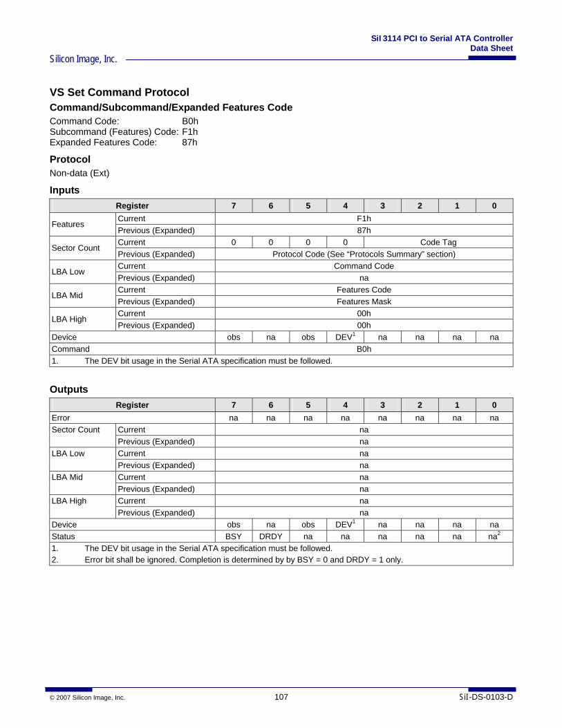
SiI3114 PCI to Serial ATA Controller Data Sheet
Silicon Image, Inc.
© 2007 Silicon Image, Inc. 107 SiI-DS-0103-D
VS Set Command Protocol Command/Subcommand/Expanded Features Code Command Code: B0h Subcommand (Features) Code: F1h Expanded Features Code: 87h
Protocol Non-data (Ext)
Inputs Register 7 6 5 4 3 2 1 0 Current F1h
Features Previous (Expanded) 87h Current 0 0 0 0 Code Tag
Sector Count Previous (Expanded) Protocol Code (See “Protocols Summary” section) Current Command Code
LBA Low Previous (Expanded) na Current Features Code
LBA Mid Previous (Expanded) Features Mask Current 00h
LBA High Previous (Expanded) 00h
Device obs na obs DEV1 na na na na Command B0h 1. The DEV bit usage in the Serial ATA specification must be followed.
Outputs Register 7 6 5 4 3 2 1 0
Error na na na na na na na na Current na Sector Count Previous (Expanded) na Current na LBA Low Previous (Expanded) na Current na LBA Mid Previous (Expanded) na Current na LBA High Previous (Expanded) na
Device obs na obs DEV1 na na na na Status BSY DRDY na na na na na na2 1. The DEV bit usage in the Serial ATA specification must be followed. 2. Error bit shall be ignored. Completion is determined by by BSY = 0 and DRDY = 1 only.
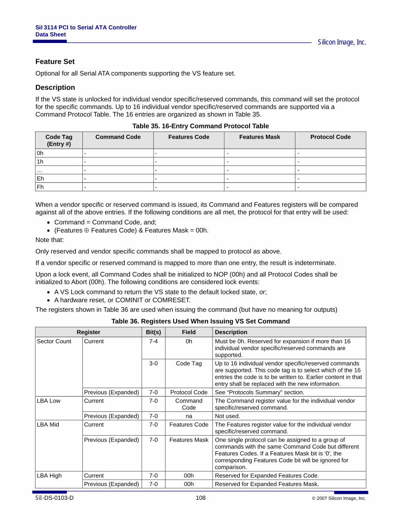
SiI3114 PCI to Serial ATA Controller Data Sheet
Silicon Image, Inc.
SiI-DS-0103-D 108 © 2007 Silicon Image, Inc.
Feature Set Optional for all Serial ATA components supporting the VS feature set.
Description If the VS state is unlocked for individual vendor specific/reserved commands, this command will set the protocol for the specific commands. Up to 16 individual vendor specific/reserved commands are supported via a Command Protocol Table. The 16 entries are organized as shown in Table 35.
Table 35. 16-Entry Command Protocol Table Code Tag (Entry #)
Command Code Features Code Features Mask Protocol Code
0h - - - - 1h - - - - ... - - - - Eh - - - - Fh - - - - When a vendor specific or reserved command is issued, its Command and Features registers will be compared against all of the above entries. If the following conditions are all met, the protocol for that entry will be used:
• Command = Command Code, and; • (Features ⊕ Features Code) & Features Mask = 00h.
Note that:
Only reserved and vendor specific commands shall be mapped to protocol as above.
If a vendor specific or reserved command is mapped to more than one entry, the result is indeterminate.
Upon a lock event, all Command Codes shall be initialized to NOP (00h) and all Protocol Codes shall be initialized to Abort (00h). The following conditions are considered lock events:
• A VS Lock command to return the VS state to the default locked state, or; • A hardware reset, or COMINIT or COMRESET.
The registers shown in Table 36 are used when issuing the command (but have no meaning for outputs)
Table 36. Registers Used When Issuing VS Set Command Register Bit(s) Field Description
7-4 0h Must be 0h. Reserved for expansion if more than 16 individual vendor specific/reserved commands are supported.
Current
3-0 Code Tag Up to 16 individual vendor specific/reserved commands are supported. This code tag is to select which of the 16 entries the code is to be written to. Earlier content in that entry shall be replaced with the new information.
Sector Count
Previous (Expanded) 7-0 Protocol Code See “Protocols Summary” section. Current 7-0 Command
Code The Command register value for the individual vendor specific/reserved command.
LBA Low
Previous (Expanded) 7-0 na Not used. Current 7-0 Features Code The Features register value for the individual vendor
specific/reserved command. LBA Mid
Previous (Expanded) 7-0 Features Mask One single protocol can be assigned to a group of commands with the same Command Code but different Features Codes. If a Features Mask bit is '0', the corresponding Features Code bit will be ignored for comparison.
Current 7-0 00h Reserved for Expanded Features Code. LBA High Previous (Expanded) 7-0 00h Reserved for Expanded Features Mask.
SiI3114 PCI to Serial ATA Controller Data Sheet
Silicon Image, Inc.
© 2007 Silicon Image, Inc. 109 SiI-DS-0103-D
A Serial ATA host, native or bridge, supporting the VS Set Command Protocol command shall use the non-data (ext) protocol with this command. The Serial ATA host shall send this command to the Serial ATA device. The following situations may happen:
Case 1: The Serial ATA device (native or bridge) responds with a completed status. Both sides are set up to support this scheme.
Case 2: The Serial ATA device bridge supports this scheme. It may optionally pass this command to a parallel ATA device:
• If passed to a parallel ATA device, the parallel ATA device responds with an abort status, which may be reported back to the Serial ATA host.
• If not passed to a parallel ATA device, the device bridge shall still respond with a device-to-host Register FIS to terminate BSY in the Serial ATA host.
However, both the Serial ATA host and the Serial ATA device bridge shall ignore the abort status and shall consider the protocol set.
The Serial ATA device is a native device and responds with an abort. The Serial ATA host will ignore the abort status and shall consider the protocol set.
In other words, regardless of the status reported (aborted or complete), the Serial ATA host and device that support this scheme shall accept the protocol as valid. State Transitions Table 37 through Table 44 describe the state transitions of the SiI3114.
Table 37. Default State - VS_LOCKED VS_LOCKED Vendor specific/Reserved commands not supported. All vendor specific
and reserved commands shall result in an ABORT status. General Protocol Code shall be 00h. Command Protocol Table initialized with all Command Codes = 00h and all Protocol Codes = 00h.
1 Received VS Unlock Vendor Specific command → VS_VS 2 Received VS Unlock Reserved command → VS_RSV 3 Received VS Unlock Individual command → VS_IND 4 Otherwise → VS_LOCKED
Table 38. VS_VS VS_VS On VS Set General Protocol command, set General Protocol Code.
Commands other than vendor specific or reserved commands shall be executed according to the predefined protocol. All vendor specific commands shall be executed according to the General Protocol Code. All reserved commands shall result in an ABORT status.
1 Received VS Unlock Reserved command → VS_VS_RSV 2 Received VS Unlock Individual command → VS_VS_IND 3 Received VS Lock command → VS_LOCKED 4 Otherwise → VS_VS
SiI3114 PCI to Serial ATA Controller Data Sheet
Silicon Image, Inc.
SiI-DS-0103-D 110 © 2007 Silicon Image, Inc.
Table 39. VS_RSV VS_RSV On VS Set General Protocol command, set General Protocol Code.
Commands other than vendor specific or reserved commands shall be executed according to the predefined protocol. All reserved commands shall be executed according to the General Protocol Code. All vendor specific commands shall result in an ABORT status.
1 Received VS Unlock Vendor Specific command → VS_VS_RSV 2 Received VS Unlock Individual command → VS_RSV_IND 3 Received VS Lock command → VS_LOCKED 4 Otherwise → VS_RSV
Table 40. VS_IND
VS_IND On VS Set Command Protocol command, update the corresponding Command Protocol Table entry. Commands other than vendor specific or reserved commands shall be executed according to the predefined protocol. All vendor specific/reserved commands with entries in the Command Protocol Table shall be executed according to the Protocol Code in the corresponding Command Protocol entry. All other commands shall result in an ABORT status.
1 Received VS Unlock Reserved command → VS_VS_RSV 2 Received VS Unlock Individual command → VS_VS_IND 3 Received VS Lock command → VS_LOCKED 4 Otherwise → VS_IND
Table 41. VS_VS_RSV
VS_VS_RSV On VS Set General Protocol command, set General Protocol Code. Commands other than vendor specific or reserved commands shall be executed according to the predefined protocol. All vendor specific/reserved commands shall be executed according to the General Protocol Code.
1 Received VS Unlock Individual command → VS_VS_RSV_IND 2 Received VS Lock command → VS_LOCKED 3 Otherwise → VS_VS_RSV
Table 42. VS_VS_IND
VS_VS_IND On VS Set General Protocol command, set General Protocol Code. On VS Set Command Protocol command, update the corresponding Command Protocol Table entry. Commands other than vendor specific or reserved commands shall be executed according to the predefined protocol. All vendor specific/reserved commands with entries in the Command Protocol Table shall be executed according to the Protocol Code in the corresponding Command Protocol entry. All other vendor specific commands shall be executed according to the General Protocol Code. All other commands shall result in an ABORT status.
1 Received VS Unlock Reserved command → VS_VS_RSV_IND 2 Received VS Lock command → VS_LOCKED 3 Otherwise → VS_VS_IND
SiI3114 PCI to Serial ATA Controller Data Sheet
Silicon Image, Inc.
© 2007 Silicon Image, Inc. 111 SiI-DS-0103-D
Table 43. VS_RSV_IND VS_RSV_IND On VS Set General Protocol command, set General Protocol Code.
On VS Set Command Protocol command, update the corresponding Command Protocol Table entry. Commands other than vendor specific or reserved commands shall be executed according to the predefined protocol. All vendor specific/reserved commands with entries in the Command Protocol Table shall be executed according to the Protocol Code in the corresponding Command Protocol entry. All reserved commands shall be executed according to the General Protocol Code. All other commands shall result in an ABORT status.
1 Received VS Unlock Vendor Specific command → VS_VS_RSV_IND 2 Received VS Lock command → VS_LOCKED 3 Otherwise → VS_RSV_IND
Table 44. VS_VS_RSV_IND
VS_VS_RSV_IND On VS Set General Protocol command, set General Protocol Code. On VS Set Command Protocol command, update the corresponding Command Protocol Table entry. Commands other than vendor specific or reserved commands shall be executed according to the predefined protocol. All vendor specific/reserved commands with entries in the Command Protocol Table shall be executed according to the Protocol Code in the corresponding Command Protocol entry. All other vendor specific/reserved commands shall be executed according to the General Protocol Code.
1 Received VS Lock command → VS_LOCKED 2 Otherwise → VS_VS_RSV_IND
SiI3114 PCI to Serial ATA Controller Data Sheet
Silicon Image, Inc.
SiI-DS-0103-D 112 © 2007 Silicon Image, Inc.
Protocols Summary The protocol encoding scheme is described in Table 45.
Table 45. Protocol Code Encoding Scheme Protocol
Code Protocol Codes Defined Bit Assignment
00h Abort 00h - 01h-3Fh A2h-AFh B3h-BFh E0h-EFh F1h-FFh
- - Reserved
40h-4Fh - - Vendor Specific
80h-8Fh C0h-CFh
(1x00xxxxb) PIO Data in/Out
80h, 81h, 82h, 87h, 88h, 89h, 8Ah, 8Bh, 8Fh, C0h, C2h, C8h,
CAh
Bit 6: 0 - legacy addressing 1 - 48-bit LBA addressing Bit 3: 0 - data in (read) 1 - data out (write) Bits 2-0: 000b - sector count is given by the Sector Count register. 001b - only one sector, Sector Count is ignored. 010b - blocks of multiple sectors, e.g., Read/Write Multiple. 011b - sector count is given by Sector Number and Sector Count registers, e.g. Download Microcode. 100b-110b - reserved 111b - 512 plus vendor specific bytes, e.g. Read/Write Long.
90h-9Fh D0h-DFh
(1x01xxxxb) DMA
90h, 91h, 98h, 99h, D0h, D1h, D8h, D9h
Bit 6: 0 - legacy addressing 1 - 48-bit LBA addressing Bit 3: 0 - data in (read) 1 - data out (write) Bits 2-1: 00b - currently defined 01b-11b - reserved. Bit 0: 0 - not queued. 1 - queued.
A0h Packet A0h - A1h Service A1h -
B0h,F0h (1x110000b)
Non-Data B0h, F0h Bit 6: 0 - legacy addressing 1 - 48-bit LBA addressing
B1h Execute Device Diagnostic B1h - B2h Device Reset B2h -
Descriptions of vendor specific protocol codes are described in Table 46 and Table 47.
SiI3114 PCI to Serial ATA Controller Data Sheet
Silicon Image, Inc.
© 2007 Silicon Image, Inc. 113 SiI-DS-0103-D
Table 46. Vendor Specific Protocol Code (in Alphabetical Order) Protocol Protocol
Code Description
Abort 00h Abort command. Status =51h and Error = 04h. Command shall not be passed to downstream device(s).
Device Reset B2h Device Reset protocol. Execute Device Diagnostic B1h Execute Device protocol (for host bridges arranged in master-slave
configuration, both shall respond regardless of the DEV bit in the Device register.
Non-Data B0h Non-Data protocol. Non-Data (Ext) F0h Non-Data (Ext) protocol. Packet A0h Packet protocol. PIO Data In (Read Multiple) 82h PIO Data In protocol for reading blocks of multiple sectors, e.g., Read
Multiple. PIO Data In (Read Multiple, Ext) C2h PIO Data In protocol for reading blocks of multiple sectors for 48-bit
LBA commands, e.g., Read Multiple Ext. PIO Data In (Sectors) 80h PIO Data In protocol, sector count is given by the Sector Count
register. PIO Data In (Sectors, Ext) C0h PIO Data In protocol for 48-bit LBA commands, sector count is given
by the Sector Count register. PIO Data In (Single Sector) 81h PIO Data In protocol, only one sector, Sector Count is ignored. PIO Data Out (Download Microcode) 8Bh PIO Data Out protocol, sector count is given by Sector Number and
Sector Count registers. PIO Data Out (Sectors) 88h PIO Data Out protocol, sector count is given by the Sector Count
register. PIO Data Out (Sectors, Ext) C8h PIO Data Out protocol for 48-bit LBA commands, sector count is given
by the Sector Count register. PIO Data Out (Single Sector) 89h PIO Data Out protocol, only one sector, Sector Count is ignored. PIO Data Out (Write Multiple) 8Ah PIO Data Out protocol for writing blocks of multiple sectors, e.g., Write
Multiple. PIO Data Out (Write Multiple, Ext) CAh PIO Data Out protocol for writing blocks of multiple sectors for 48-bit
LBA commands, e.g., Write Multiple Ext Read DMA 90h Read DMA protocol. Read DMA (Ext) D0h Read DMA protocol for 48-bit LBA commands. Read DMA Queued 91h Read DMA Queued protocol. Read DMA Queued (Ext) D1h Read DMA Queued for 48-bit LBA commands. Read Long 87h PIO Data In protocol, 512 plus vendor specific bytes, e.g. Read Long. Service A1h Service protocol. Write DMA 98h Write DMA protocol. Write DMA (Ext) D8h Write DMA protocol for 48-bit LBA commands. Write DMA queued 99h Write DMA queued protocol. Write DMA queued (Ext) D9h Write DMA queued for 48-bit LBA commands. Write Long 8Fh PIO Data Out protocol, 512 plus vendor specific bytes, e.g. Write Long
SiI3114 PCI to Serial ATA Controller Data Sheet
Silicon Image, Inc.
SiI-DS-0103-D 114 © 2007 Silicon Image, Inc.
Table 47. Vendor Specific Protocol Code (by Protocol Code) Protocol
Code Protocol Description
00h Abort Abort command. Status =51h and Error = 04h. Command shall not be passed to downstream device(s).
80h PIO Data In (Sectors) PIO Data In protocol, sector count is given by the Sector Count register.
81h PIO Data In (Single Sector) PIO Data In protocol, only one sector, Sector Count is ignored. 82h PIO Data In (Read Multiple) PIO Data In protocol for reading blocks of multiple sectors, e.g., Read
Multiple. 87h Read Long PIO Data In protocol, 512 plus vendor specific bytes, e.g. Read Long.88h PIO Data Out (Sectors) PIO Data Out protocol, sector count is given by the Sector Count
register. 89h PIO Data Out (Single Sector) PIO Data Out protocol, only one sector, Sector Count is ignored. 8Ah PIO Data Out (Write Multiple) PIO Data Out protocol for writing blocks of multiple sectors, e.g.,
Write Multiple. 8Bh PIO Data Out (Download Microcode) PIO Data Out protocol, sector count is given by Sector Number and
Sector Count registers. 8Fh Write Long PIO Data Out protocol, 512 plus vendor specific bytes, e.g. Write
Long 90h Read DMA Read DMA protocol. 91h Read DMA Queued Read DMA Queued protocol. 98h Write DMA Write DMA protocol. 99h Write DMA queued Write DMA queued protocol. A0h Packet Packet protocol. A1h Service Service protocol. B0h Non-Data Non-Data protocol. B1h Execute Device Diagnostic Execute Device protocol (for host bridges arranged in master-slave
configuration, both shall respond regardless of the DEV bit in the Device register.
B2h Device Reset Device Reset protocol. C0h PIO Data In (Sectors, Ext) PIO Data In protocol for 48-bit LBA commands, sector count is given
by the Sector Count register. C2h PIO Data In (Read Multiple, Ext) PIO Data In protocol for reading blocks of multiple sectors for 48-bit
LBA commands, e.g., Read Multiple Ext. C8h PIO Data Out (Sectors, Ext) PIO Data Out protocol for 48-bit LBA commands, sector count is
given by the Sector Count register. CAh PIO Data Out (Write Multiple, Ext) PIO Data Out protocol for writing blocks of multiple sectors for 48-bit
LBA commands, e.g., Write Multiple Ext D0h Read DMA (Ext) Read DMA protocol for 48-bit LBA commands. D1h Read DMA Queued (Ext) Read DMA Queued for 48-bit LBA commands. D8h Write DMA (Ext) Write DMA protocol for 48-bit LBA commands. D9h Write DMA queued (Ext) Write DMA queued for 48-bit LBA commands. F0h Non-Data (Ext) Non-Data (Ext) protocol.
SiI3114 PCI to Serial ATA Controller Data Sheet
Silicon Image, Inc.
© 2007 Silicon Image, Inc. 115 SiI-DS-0103-D
Table 48. Vendor Specific Protocol Code (in Alphabetical Order) Protocol Protocol
Code Command Examples
Abort 00h Any unsupported commands Device Reset B2h Device Reset Execute Device Diagnostic B1h Execute Device Diagnostics Non-Data B0h CFA Erase Sectors, CFA Request Extended Error Code, Check
Media Card Type, Check Power Mode, Device Configuration Restore, Device Configuration Freeze Lock, Flush Cache, Get Media Status, Idle, Idle Immediate, Initialize Device Parameters, Media Eject, Media Lock, Media Unlock, Nop, Read Native Max Address, Read Verify Sector(s), ReadFPDMAQueued, Recalibrate, Security Erase Prepare, Security Freeze Lock, Seek, Set Features, Set Max Address, Set Max Lock, Set Max Freeze Lock, Set Multiple Mode, Sleep, Smart Disable Operations,Smart Enable/Disable Attributes Autosave, Smart Enable Operations, Smart Execute Off-Line Immediate, Smart Return Status, Smart Save Attribute Values, Standby, Standby Immediate, WriteFPDMAQueued
Non-Data (Ext) F0h Configure Stream, Flush Cache Extended, Read Native Max Address Ext, Read Verify Sector(s) Ext, Set Max Address Ext
Packet A0h Packet PIO Data In (Read Multiple) 82h Read Multiple PIO Data In (Read Multiple, Ext) C2h Read Multiple Ext PIO Data In (Sectors) 80h Read Sector(s), Smart Read Log PIO Data In (Sectors, Ext) C0h Read Log Ext, Read Sector(s) Ext, Read Stream PIO PIO Data In (Single Sector) 81h CFA Translate Sector, CleanupAndRequestSense, Device
Configuration Identify, Identify Device, Identify Packet Device, Read Buffer, Security Set Password, Security Unlock, Set Max Set Password, Smart Read Attribute Thresholds, Smart Read Data
PIO Data Out (Download Microcode) 8Bh Download Microcode PIO Data Out (Sectors) 88h CFA Write Sectors without Erase, Smart Write Log, Write
Sector(s) PIO Data Out (Sectors, Ext) C8h Write Sector(s) Ext PIO Data Out (Single Sector) 89h Device Configuration Set, Security Disable Password, Security
Erase Unit, Write Buffer PIO Data Out (Write Multiple) 8Ah CFA Write Multiple without Erase, Write Multiple PIO Data Out (Write Multiple, Ext) CAh Write Log Ext, Write Multiple Ext, Write Stream PIO Read DMA 90h Read DMA Read DMA (Ext) D0h Read DMA Ext, Read Stream DMA Read DMA Queued 91h Read DMA Queued Read DMA Queued (Ext) D1h Read DMA Queued Ext Read Long 87h Read Long Service A1h Service Write DMA 98h Write DMA Write DMA (Ext) D8h Write DMA Ext, Write Stream DMA Write DMA queued 99h Write DMA Queued Write DMA queued (Ext) D9h Write DMA Queued Ext Write Long 8Fh Write Long
SiI3114 PCI to Serial ATA Controller Data Sheet
Silicon Image, Inc.
SiI-DS-0103-D 116 © 2007 Silicon Image, Inc.
Reading and Writing of Task File and Device Control Registers 48-Bit LBA Addressing The SiI3114 supports 48-bit LBA. The SiI3114 does not differentiate a non-extended command (one that does not use 48-bit LBA address) from an extended command (one that uses the 48-bit LBA address). The "expanded" registers can be read with the HOB bit of the Device Control register se to '1'.
Device Control Register and Soft Reset When the Device Control register is written, a Register FIS for Control will be sent downstream upon one of the following conditions:
• There is a change in the SRST bit, or; • With SRST bit being '0', there is a change in the NIEN bit.
Note that: • When the SRST is '1', the NIEN bit in the Register FIS sent is insignificant. • Any change in the HOB bit will not initiate any Register FIS to be sent. In fact, HOB bit is always '0' in the
Register FIS sent. • If the Serial ATA channel is in PARTIAL or SLUMBER state, a COMWAKE will be automatically initiated to
wake up the channel before the Register FIS is sent. However, the channel will stay at the ON state at the end of the operation, even if no soft reset occurs.
A soft reset will do the following: • Wake up the downstream Serial ATA device from ATA IDLE, STANDBY or SLEEP.
LED Support The SiI3114 supports four activity LEDs via four 12mA open-drain drivers LED[0..3]. LED0 is to indicate activity in channel 0; LED1 in channel 1; LED2 in channel 2; and LED3 in channel3.
When there is activity for a non-ATAPI device, as indicated by: • BSY in the ATA Status being set, or; • Any bit in the Serial ATA SActive register being set
… the corresponding LED driver outputs will be driven low.
There is no activity LED support for ATAPI device. If the downstream device is an ATAPI device, the corresponding LED output will not be driven low.

SiI3114 PCI to Serial ATA Controller Data Sheet
Silicon Image, Inc.
© 2007 Silicon Image, Inc. 117 SiI-DS-0103-D
Flash and EEPROM Programming Sequences Flash Memory Access The SiI3114 supports an external flash memory device up to 4 Mbit in capacity. Access to the Flash memory is available through two means: PCI Direct Access and Register Access.
PCI Direct Access Access to the Expansion Rom is enabled by setting bit 0 in the Expansion Rom Base Address register at Offset 30h of the PCI Configuration Space. When this bit is set, bits [31:19] of the same register are programmable by the system to set the base address for all Flash memory accesses. Read and write operations with the flash memory are initiated by Memory Read and Memory Write commands on the PCI bus. Accesses may be as bytes, words, or dwords.
Register Access This type of flash memory access is carried out through a sequence of internal register read and write operations. The proper programming sequences are detailed below.
Flash Write Operation Verify that bit 25 is cleared in the register at Offset 50H of Base Address 5. The bit reads one when a memory access is currently in progress.
It reads zero when the memory access is complete and ready for another operation.
Program the write address for the Flash memory access. The address field is defined by bits [18:00] in the Flash Memory Address – Command + Status register.
Program the write data for the Flash memory access. The data field is defined by bits [07:00] in the Flash Memory Data register at Offset 54 of Base Address 5.
Program the memory access type. The memory access type is defined by bit 24 in the Flash Memory Address – Command + Status register. The bit must be cleared for a memory write access.
Initiate the Flash memory access by setting bit 25 in the Flash Memory Address – Command + Status register.
Flash Read Operation Verify that bit 25 is cleared in the Flash Memory Address – Command + Status register at Offset 50H of Base Address 5. The bit reads one when a memory access is currently in progress. It reads zero when the memory access is complete and ready for another operation.
Program the read address for the Flash memory access. The address field is defined by bits [18:00] in the Flash Memory Address – Command + Status register.
Program the memory access type. The memory access type is defined by bit 24 in the Flash Memory Address – Command + Status register. The bit must be set for a memory read access.
Initiate the Flash memory access by setting bit 25 in the Flash Memory Address – Command + Status register.
Verify that bit 25 is cleared in the Flash Memory Address – Command + Status register. The bit reads one when a memory access is currently in progress. It reads zero when the memory access is complete.
Read the data from the Flash memory access. The data field is defined by bits [07:00] in the Flash Memory Data register at Offset 54H of Base Address 5.
SiI3114 PCI to Serial ATA Controller Data Sheet
Silicon Image, Inc.
SiI-DS-0103-D 118 © 2007 Silicon Image, Inc.
EEPROM Memory Access The SiI3114 supports an external 256-byte EEPROM memory device. Access to the EEPROM memory is available through internal register operations in the SiI3114.
EEPROM Write Operation Verify that bit 25 is cleared in the EEPROM Memory Address – Command + Status register at Offset 58H of Base Address 5. The bit reads one when a memory access is currently in progress. It reads zero when the memory access is complete and ready for another operation.
Write ‘1’ to clear bit 28 in the EEPROM Memory Address – Command + Status register. The bit is set if an error occurred during a previous memory access.
Program the write address for the EEPROM memory access. The address field is defined by bits [07:00] in the EEPROM Memory Address – Command + Status register. Program bits [15:08] to zero.
Program the write data for the EEPROM memory access. The data field is defined by bits [07:00] in the EEPROM Memory Data register at Offset 5CH of Base Address 5.
Program the memory access type. The memory access type is defined by bit 24 in the EEPROM Memory Address – Command + Status register. The bit must be cleared for a memory write access.
Initiate the EEPROM memory access by setting bit 25 in the EEPROM Memory Address – Command + Status register.
Poll bit 25 in the EEPROM Memory Address – Command + Status register. The bit reads one when a memory access is currently in progress. It reads zero when the memory access is complete.
Check bit 28 in the EEPROM Memory Address – Command + Status register. The bit is set if an error occurred during a previous memory access.
EEPROM Read Operation Verify that bit 25 is cleared in the EEPROM Memory Address – Command + Status register at Offset 58H of Base Address 5. The bit reads one when a memory access is currently in progress. It reads zero when the memory access is complete and ready for another operation.
Write ‘1’ to clear bit 28 in the EEPROM Memory Address – Command + Status register. The bit is set if an error occurred during a previous memory access.
Program the read address for the EEPROM memory access. The address field is defined by bits [07:00] in the EEPROM Memory Address – Command + Status register. Program bits [15:08] to zero.
Program the memory access type. The memory access type is defined by bit 24 in the EEPROM Memory Address – Command + Status register. The bit must be set for a memory read access.
Initiate the EEPROM memory access by setting bit 25 in the EEPROM Memory Address – Command + Status register.
Poll bit 25 in the EEPROM Memory Address – Command + Status register. The bit reads one when a memory access is currently in progress. It reads zero when the memory access is complete.
Check bit 28 in the EEPROM Memory Address – Command + Status register. The bit is set if an error occurred during a previous memory access.
Read the data from the EEPROM memory access. The data field is defined by bits [07:00] in the EEPROM Memory Data register at Offset 5CH of Base Address 5.
SiI3114 PCI to Serial ATA Controller Data Sheet
Silicon Image, Inc.
© 2007 Silicon Image, Inc. 119 SiI-DS-0103-D
Disclaimers These materials are provided on an “AS IS” basis. Silicon Image, Inc. and its affiliates disclaim all representations and warranties (express, implied, statutory or otherwise), including but not limited to: (i) all implied warranties of merchantability, fitness for a particular purpose, and/or non-infringement of third party rights; (ii) all warranties arising out of course-of-dealing, usage, and/or trade; and (iii) all warranties that the information or results provided in, or that may be obtained from use of, the materials are accurate, reliable, complete, up-to-date, or produce specific outcomes. Silicon Image, Inc. and its affiliates assume no liability or responsibility for any errors or omissions in these materials, makes no commitment or warranty to correct any such errors or omissions or update or keep current the information contained in these materials, and expressly disclaims all direct, indirect, special, incidental, consequential, reliance and punitive damages, including WITHOUT LIMITATION any loss of profits arising out of your access to, use or interpretation of, or actions taken or not taken based on the content of these materials.
Silicon Image, Inc. and its affiliates reserve the right, without notice, to periodically modify the information in these materials, and to add to, delete, and/or change any of this information.
Notwithstanding the foregoing, these materials shall not, in the absence of authorization under U.S. and local law and regulations, as required, be used by or exported or re-exported to (i) any U.S. sanctioned or embargoed country, or to nationals or residents of such countries; or (ii) any person, entity, organization or other party identified on the U.S. Department of Commerce's Denied Persons or Entity List, the U.S. Department of Treasury's Specially Designated Nationals or Blocked Persons List, or the Department of State's Debarred Parties List, as published and revised from time to time; (iii) any party engaged in nuclear, chemical/biological weapons or missile proliferation activities; or (iv) any party for use in the design, development, or production of rocket systems or unmanned air vehicles.
Products and Services The products and services described in these materials, and any other information, services, designs, know-how and/or products provided by Silicon Image, Inc. and/or its affiliates are provided on as “AS IS” basis, except to the extent that Silicon Image, Inc. and/or its affiliates provides an applicable written limited warranty in its standard form license agreements, standard Terms and Conditions of Sale and Service or its other applicable standard form agreements, in which case such limited warranty shall apply and shall govern in lieu of all other warranties (express, statutory, or implied). EXCEPT FOR SUCH LIMITED WARRANTY, SILICON IMAGE, INC. AND ITS AFFILIATES DISCLAIM ALL REPRESENTATIONS AND WARRANTIES (EXPRESS, IMPLIED, STATUTORY OR OTHERWISE), REGARDING THE INFORMATION, SERVICES, DESIGNS, KNOW-HOW AND PRODUCTS PROVIDED BY SILICON IMAGE, INC. AND/OR ITS AFFILIATES, INCLUDING BUT NOT LIMITED TO, ALL IMPLIED WARRANTIES OF MERCHANTABILITY, FITNESS FOR A PARTICULAR PURPOSE, AND/OR NON-INFRINGEMENT OF THIRD PARTY RIGHTS. YOU ACKNOWLEDGE AND AGREE THAT SUCH INFORMATION, SERVICES, DESIGNS, KNOW-HOW AND PRODUCTS HAVE NOT BEEN DESIGNED, TESTED, OR MANUFACTURED FOR USE OR RESALE IN SYSTEMS WHERE THE FAILURE, MALFUNCTION, OR ANY INACCURACY OF THESE ITEMS CARRIES A RISK OF DEATH OR SERIOUS BODILY INJURY, INCLUDING, BUT NOT LIMITED TO, USE IN NUCLEAR FACILITIES, AIRCRAFT NAVIGATION OR COMMUNICATION, EMERGENCY SYSTEMS, OR OTHER SYSTEMS WITH A SIMILAR DEGREE OF POTENTIAL HAZARD. NO PERSON IS AUTHORIZED TO MAKE ANY OTHER WARRANTY OR REPRESENTATION CONCERNING THE PERFORMANCE OF THE INFORMATION, PRODUCTS, KNOW-HOW, DESIGNS OR SERVICES OTHER THAN AS PROVIDED IN THESE TERMS AND CONDITIONS.
1060 E. Arques Avenue
Sunnyvale, CA 94085 T 408.616.4000 F 408.830.9530
www.siliconimage.com