Signal and Power Integrity Practices - indico.cern.ch · PH-ESE seminar, 9/6/2015 Csaba SOOS,...
55
Signal and Power Integrity Design Practices Csaba SOOS PH-ESE-BE
Transcript of Signal and Power Integrity Practices - indico.cern.ch · PH-ESE seminar, 9/6/2015 Csaba SOOS,...
Signal and Power Integrity Design Practices
Csaba SOOS
PH-ESE-BE

Outline
• Introduction
• Signal and interconnect bandwidth
• Time and frequency• Scattering parameters
• Transmission lines• Theory
• Losses, ISI, discontinuities, crosstalk, mode conversion
• Power Delivery Network
• Related activities in the group
PH-ESE seminar, 9/6/2015 Csaba SOOS, Signal and Power Integrity Design Practices 2
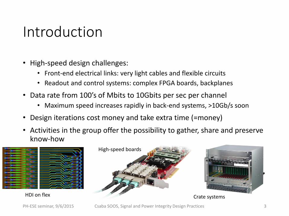
Introduction
• High-speed design challenges:• Front-end electrical links: very light cables and flexible circuits
• Readout and control systems: complex FPGA boards, backplanes
• Data rate from 100’s of Mbits to 10Gbits per sec per channel• Maximum speed increases rapidly in back-end systems, >10Gb/s soon
• Design iterations cost money and take extra time (=money)
• Activities in the group offer the possibility to gather, share and preserve know-how
HDI on flex
High-speed boards
Crate systems
PH-ESE seminar, 9/6/2015 Csaba SOOS, Signal and Power Integrity Design Practices 3
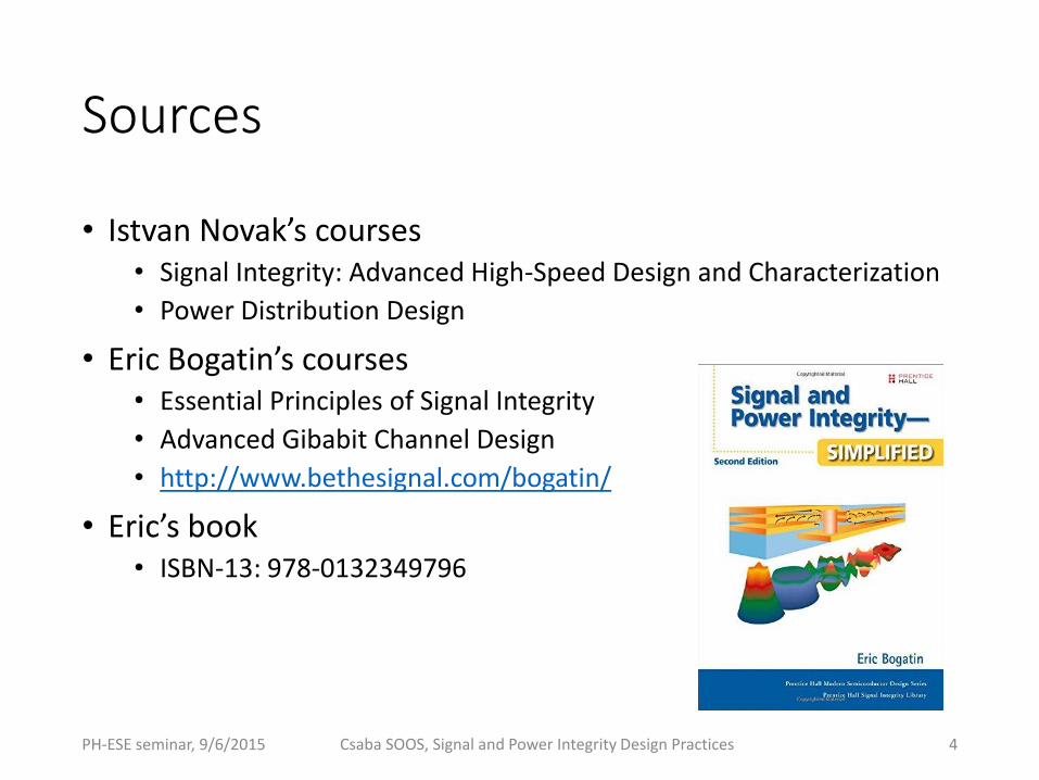
Sources
• Istvan Novak’s courses• Signal Integrity: Advanced High-Speed Design and Characterization
• Power Distribution Design
• Eric Bogatin’s courses• Essential Principles of Signal Integrity
• Advanced Gibabit Channel Design
• http://www.bethesignal.com/bogatin/
• Eric’s book• ISBN-13: 978-0132349796
PH-ESE seminar, 9/6/2015 Csaba SOOS, Signal and Power Integrity Design Practices 4

Signal bandwidth
• Time domain: periodic signal (e.g. clock)• Period, T
• Rise/fall times, tr/tf
• Duty cycle, D
• Time-domain to frequency domain using Fouriertransformation
• Spectrum of an ideal square wave (D=0.5, tr/tf = 0) • DC (0th harmonic) + infinite odd harmonics (1,3,5…)
• Amplitudes decrease with 1/f (-6dB/octave), An=(2 x A)/(π x n)
DT (1-D)T
Vlo
Vhi
T = 1/Fo
A = Vhi - Vlo
tr tf
PH-ESE seminar, 9/6/2015 Csaba SOOS, Signal and Power Integrity Design Practices 5
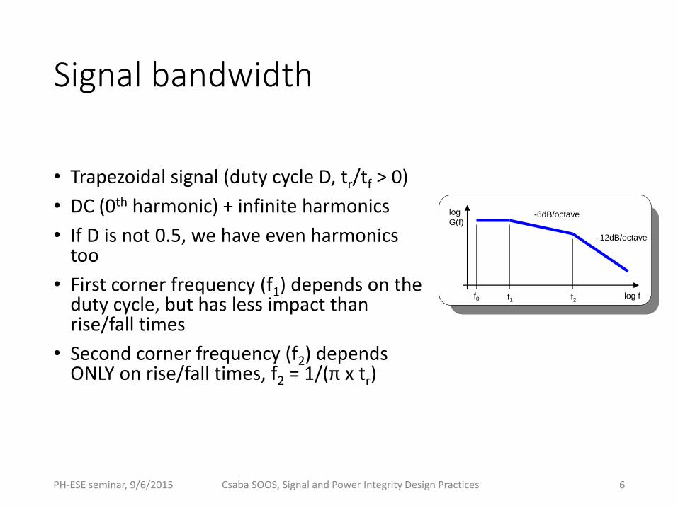
Signal bandwidth
• Trapezoidal signal (duty cycle D, tr/tf > 0)
• DC (0th harmonic) + infinite harmonics
• If D is not 0.5, we have even harmonics too
• First corner frequency (f1) depends on the duty cycle, but has less impact than rise/fall times
• Second corner frequency (f2) depends ONLY on rise/fall times, f2 = 1/(π x tr)
f0 f1 f2
-6dB/octave
-12dB/octave
log f
log
G(f)
PH-ESE seminar, 9/6/2015 Csaba SOOS, Signal and Power Integrity Design Practices 6

Signal bandwidth
• How many harmonics should be preserved ?
• First approach• Use only harmonics which are more than 70% of the amplitude (-3dB) of
the equivalent ideal square wave => e.g. up to 5th harmonic
• Second approach• Sum up harmonics until the rise/fall time reaches required value =>
BW=0.35/tr(10-90), or BW=0.22/tr(20-80) which is about the same as the second corner frequency
• Do not use higher bandwidth than required, because it costs money
PH-ESE seminar, 9/6/2015 Csaba SOOS, Signal and Power Integrity Design Practices 7

Bandwidth of the interconnect
• The bandwidth definition is subjective• Highest sine-wave frequency at which the interconnect still meets the
specs.
• We typically use -3 dB => 70% of the incident amplitude
• Bandwidth limitation increases rise time𝑅𝑇𝑜𝑢𝑡 = 𝑅𝑇𝑖𝑛 + 𝑅𝑇𝑐ℎ𝑎𝑛𝑛𝑒𝑙
• To quantify, we can use the frequency dependent Insertion Loss of the interconnect
f0 f1 f2
-6dB/octave
-12dB/octave
log f
log
G(f)
f
log
H(f)
= ?+
PH-ESE seminar, 9/6/2015 Csaba SOOS, Signal and Power Integrity Design Practices 8
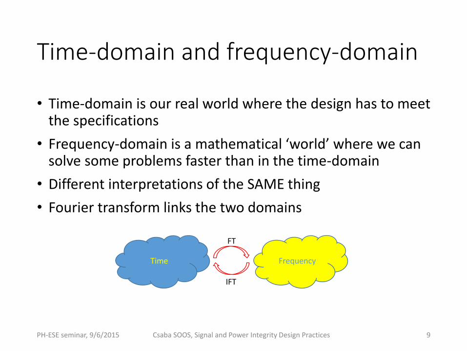
Time-domain and frequency-domain
• Time-domain is our real world where the design has to meet the specifications
• Frequency-domain is a mathematical ‘world’ where we can solve some problems faster than in the time-domain
• Different interpretations of the SAME thing
• Fourier transform links the two domains
Time Frequency
FT
IFT
PH-ESE seminar, 9/6/2015 Csaba SOOS, Signal and Power Integrity Design Practices 9

Scattering or S-parameters
• Behavioural model of N-port linear electrical networks
• Frequency domain description• Sine wave in, sine wave out
• Inherited from RF and now widely used by SI/PI engineers
N-portNetwork
a1
b1aN
bN
𝑏 = 𝐒 𝑎
2-port network
𝑏1
𝑏2=
𝑆11 𝑆12
𝑆21 𝑆22
𝑎1
𝑎2
𝑏1 = 𝑆11𝑎1 + 𝑆12𝑎2
𝑏2 = 𝑆21𝑎1 + 𝑆22𝑎2
Sij
output input
PH-ESE seminar, 9/6/2015 Csaba SOOS, Signal and Power Integrity Design Practices 10

S-parameter plots (frequency domain)
• S11 should be large negative number if the port is matched to the reference impedance• Mag(S21) shows the frequency dependent loss (FOM dB/inch/Hz)• Ang(S21) should start from 0 and decrease with increasing frequency (saw tooth)
PH-ESE seminar, 9/6/2015 Csaba SOOS, Signal and Power Integrity Design Practices 11

S-parameters (time domain)
Impedance (TDR) Step response (TDT) Impulse response (TDT)
PH-ESE seminar, 9/6/2015 Csaba SOOS, Signal and Power Integrity Design Practices 12
S parameters can be converted back to time domain (IFFT). Some artifacts mayappear if the S parameter data does not meet certain criteria.

Mixed-mode S-parameters
Single-ended S parameters can be converted to mixed-mode S parametersto describe differential signals.
PH-ESE seminar, 9/6/2015 Csaba SOOS, Signal and Power Integrity Design Practices 13
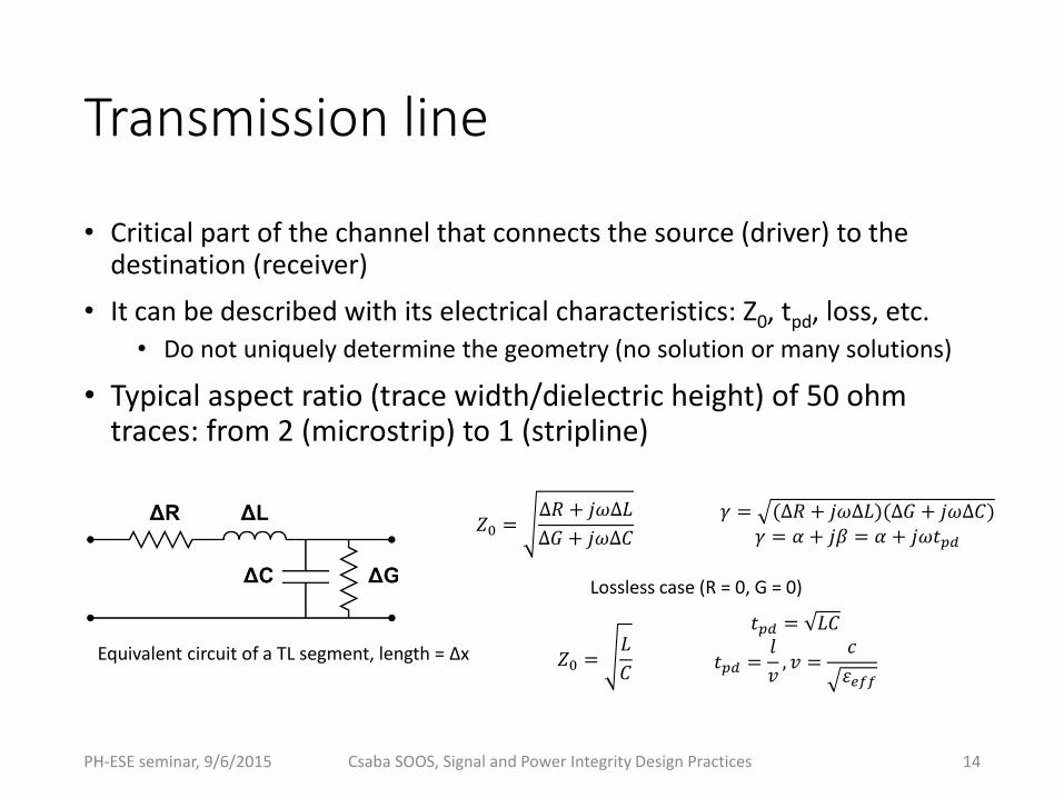
Transmission line
• Critical part of the channel that connects the source (driver) to the destination (receiver)
• It can be described with its electrical characteristics: Z0, tpd, loss, etc.• Do not uniquely determine the geometry (no solution or many solutions)
• Typical aspect ratio (trace width/dielectric height) of 50 ohm traces: from 2 (microstrip) to 1 (stripline)
𝑍0 =∆𝑅 + 𝑗𝜔∆𝐿
∆𝐺 + 𝑗𝜔∆𝐶
𝛾 = (∆𝑅 + 𝑗𝜔∆𝐿)(∆𝐺 + 𝑗𝜔∆𝐶)𝛾 = 𝛼 + 𝑗𝛽 = 𝛼 + 𝑗𝜔𝑡𝑝𝑑
𝑍0 =𝐿
𝐶
𝑡𝑝𝑑 = 𝐿𝐶
𝑡𝑝𝑑 =𝑙
𝑣, 𝑣 =
𝑐
𝜀𝑒𝑓𝑓
Lossless case (R = 0, G = 0)
Equivalent circuit of a TL segment, length = Δx
PH-ESE seminar, 9/6/2015 Csaba SOOS, Signal and Power Integrity Design Practices 14
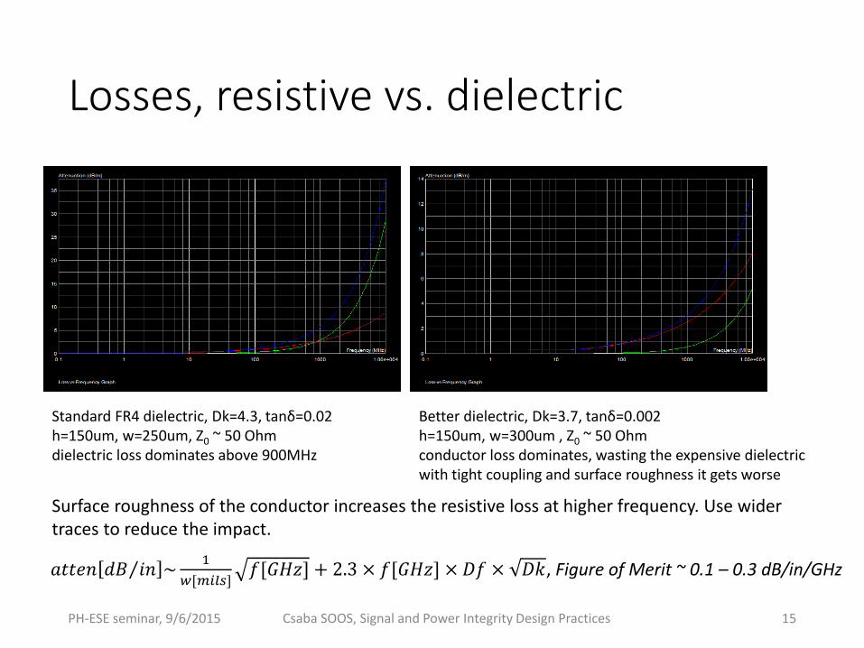
Losses, resistive vs. dielectric
Better dielectric, Dk=3.7, tanδ=0.002h=150um, w=300um , Z0 ~ 50 Ohmconductor loss dominates, wasting the expensive dielectricwith tight coupling and surface roughness it gets worse
Standard FR4 dielectric, Dk=4.3, tanδ=0.02h=150um, w=250um, Z0 ~ 50 Ohmdielectric loss dominates above 900MHz
PH-ESE seminar, 9/6/2015 Csaba SOOS, Signal and Power Integrity Design Practices 15
Surface roughness of the conductor increases the resistive loss at higher frequency. Use widertraces to reduce the impact.
𝑎𝑡𝑡𝑒𝑛 𝑑𝐵 𝑖𝑛 ~1
𝑤[𝑚𝑖𝑙𝑠]𝑓[𝐺𝐻𝑧] + 2.3 × 𝑓[𝐺𝐻𝑧] × 𝐷𝑓 × 𝐷𝑘, Figure of Merit ~ 0.1 – 0.3 dB/in/GHz

Coupled traces, differential impedance
200um
400um
FR4, Dk=4.3, tanδ=0.02
Coupled microstrip traces
Coupled stripline traces
PH-ESE seminar, 9/6/2015 Csaba SOOS, Signal and Power Integrity Design Practices 16
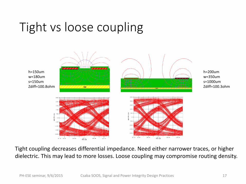
Tight vs loose coupling
HyperLynx v8.2.1
GND
h=150umw=180ums=150umZdiff=100.8ohm
HyperLynx v8.2.1
GND
h=200umw=350ums=1000umZdiff=100.3ohm
Tight coupling decreases differential impedance. Need either narrower traces, or higherdielectric. This may lead to more losses. Loose coupling may compromise routing density.
PH-ESE seminar, 9/6/2015 Csaba SOOS, Signal and Power Integrity Design Practices 17

Loss in coupled microstrip traces
Judging the loss of the interconnect using only S21 is difficult, if traces are coupled.If the coupling is intentional (differential trace), use SDD21 instead.
Tight coupling Loose coupling
S21 S41
Sdd21 Sdd21
S21S41
PH-ESE seminar, 9/6/2015 Csaba SOOS, Signal and Power Integrity Design Practices 18
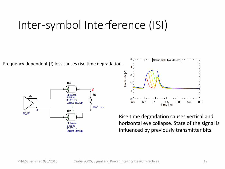
Inter-symbol Interference (ISI)
Design File: Losses_time_domain
HyperLynx LineSim v8.2.1
TL1
51.1 ohms2.413 ns40.000 cmCoupled Stackup
U1
TX_diff
2
1
TL2
51.1 ohms2.413 ns40.000 cmCoupled Stackup
R1
100.0 ohms
Rise time degradation causes vertical and horizontal eye collapse. State of the signal is influenced by previously transmitter bits.
Frequency dependent (!) loss causes rise time degradation.
PH-ESE seminar, 9/6/2015 Csaba SOOS, Signal and Power Integrity Design Practices 19
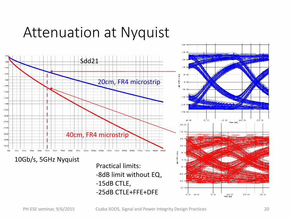
Attenuation at Nyquist
PH-ESE seminar, 9/6/2015 Csaba SOOS, Signal and Power Integrity Design Practices 20
10Gb/s, 5GHz Nyquist
20cm, FR4 microstrip
40cm, FR4 microstrip
Practical limits:-8dB limit without EQ,-15dB CTLE,-25dB CTLE+FFE+DFE
Sdd21
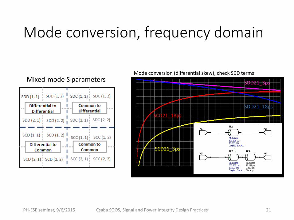
Mode conversion, frequency domain
Design File: S_params_mode_conversion
HyperLynx LineSim v8.2.1
TL1
51.1 ohms603.206 ps10.000 cmCoupled Stackup
N1 N2
TL2
51.1 ohms603.206 ps10.000 cmCoupled Stackup
N3 N4TL3
51.2 ohms18.112 ps0.300 cmStackup
Mode conversion (differential skew), check SCD terms
SCD21_3ps
SCD21_18ps
SDD21_18ps
SDD21_3psMixed-mode S parameters
PH-ESE seminar, 9/6/2015 Csaba SOOS, Signal and Power Integrity Design Practices 21

Mode conversion, time domain
No skew 18ps skew
Differential
Common
Differential
Common
PH-ESE seminar, 9/6/2015 Csaba SOOS, Signal and Power Integrity Design Practices 22

Mode conversion summary
• There is no perfect interconnection, there is always mode conversion• Skew (driver, traces, connectors, PCB dielectric etc.), asymmetries
• Issues related to mode conversion• Distorted differential signal, EMI, ISI (reflected common signal
converts back to differential)
• Solutions• Reduce skew to achieve << 10% UI, match near mismatch
• Terminate common signal (no conversion back to differential)
• Use symmetrical ground return vias (GSSG)
• Use better dielectric glass weave (1086, 3313), better glass fill or zig-zag routing
PH-ESE seminar, 9/6/2015 Csaba SOOS, Signal and Power Integrity Design Practices 23
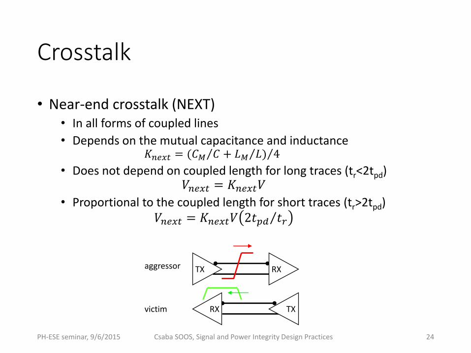
Crosstalk
• Near-end crosstalk (NEXT)• In all forms of coupled lines
• Depends on the mutual capacitance and inductance𝐾𝑛𝑒𝑥𝑡 = ( 𝐶𝑀 𝐶 + 𝐿𝑀 𝐿) 4
• Does not depend on coupled length for long traces (tr<2tpd)𝑉𝑛𝑒𝑥𝑡 = 𝐾𝑛𝑒𝑥𝑡𝑉
• Proportional to the coupled length for short traces (tr>2tpd)𝑉𝑛𝑒𝑥𝑡 = 𝐾𝑛𝑒𝑥𝑡𝑉 2𝑡𝑝𝑑 𝑡𝑟
TX RX
RX TX
aggressor
victim
PH-ESE seminar, 9/6/2015 Csaba SOOS, Signal and Power Integrity Design Practices 24
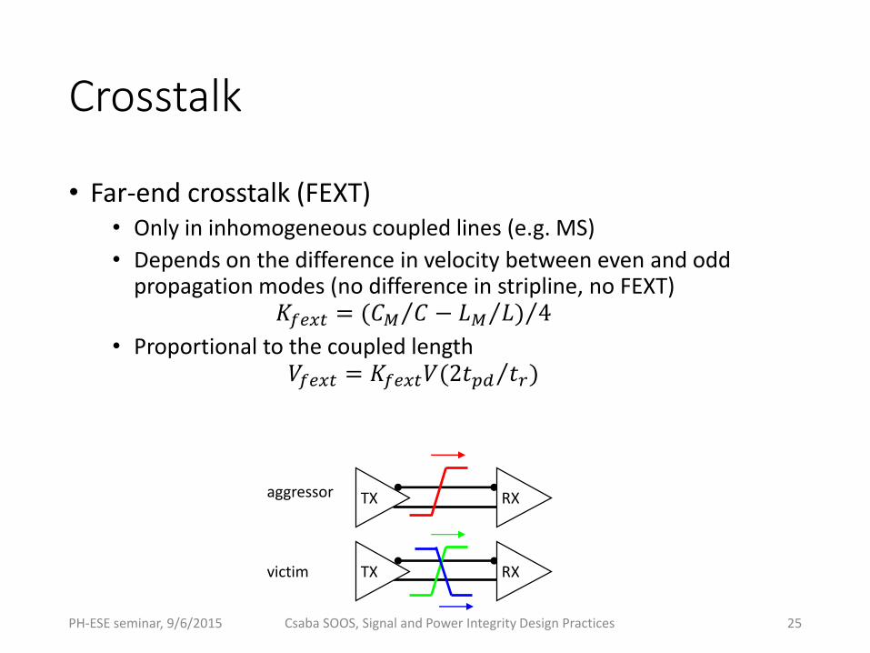
Crosstalk
• Far-end crosstalk (FEXT)• Only in inhomogeneous coupled lines (e.g. MS)
• Depends on the difference in velocity between even and odd propagation modes (no difference in stripline, no FEXT)
𝐾𝑓𝑒𝑥𝑡 = ( 𝐶𝑀 𝐶 − 𝐿𝑀 𝐿) 4
• Proportional to the coupled length𝑉𝑓𝑒𝑥𝑡 = 𝐾𝑓𝑒𝑥𝑡𝑉( 2𝑡𝑝𝑑 𝑡𝑟)
TX RXaggressor
victim TX RX
PH-ESE seminar, 9/6/2015 Csaba SOOS, Signal and Power Integrity Design Practices 25
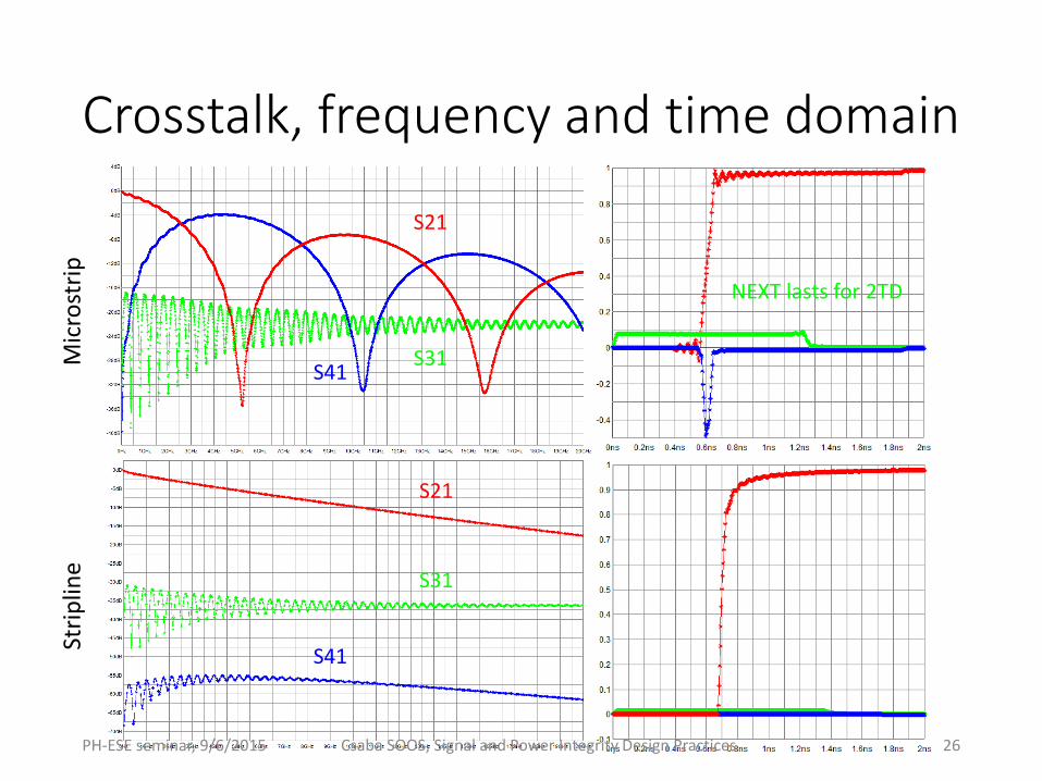
Crosstalk, frequency and time domainM
icro
stri
pSt
rip
line
S21
S21
S31
S31S41
S41
NEXT lasts for 2TD
PH-ESE seminar, 9/6/2015 Csaba SOOS, Signal and Power Integrity Design Practices 26

Crosstalk, frequency and time domainM
icro
stri
pSt
rip
line
S21
S21
S31
S31S41
S41
FEXT in UI
No FEXT
PH-ESE seminar, 9/6/2015 Csaba SOOS, Signal and Power Integrity Design Practices 27
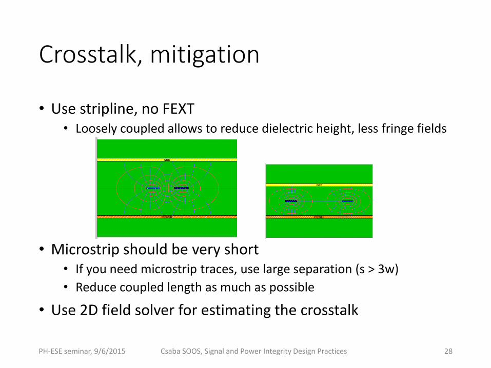
Crosstalk, mitigation
• Use stripline, no FEXT• Loosely coupled allows to reduce dielectric height, less fringe fields
• Microstrip should be very short• If you need microstrip traces, use large separation (s > 3w)
• Reduce coupled length as much as possible
• Use 2D field solver for estimating the crosstalk
PH-ESE seminar, 9/6/2015 Csaba SOOS, Signal and Power Integrity Design Practices 28
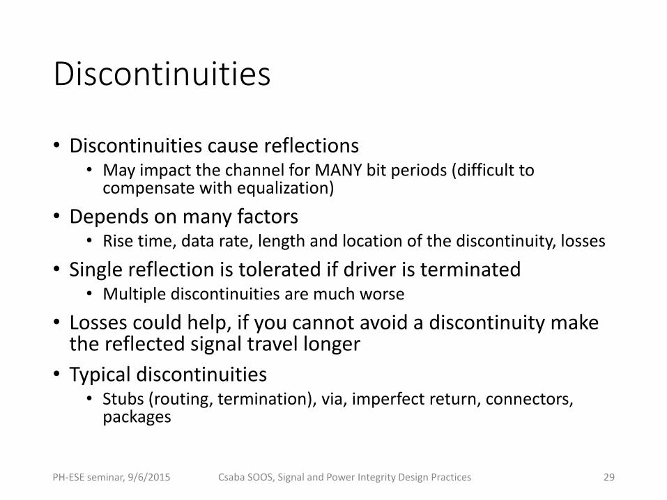
Discontinuities
• Discontinuities cause reflections• May impact the channel for MANY bit periods (difficult to
compensate with equalization)
• Depends on many factors• Rise time, data rate, length and location of the discontinuity, losses
• Single reflection is tolerated if driver is terminated• Multiple discontinuities are much worse
• Losses could help, if you cannot avoid a discontinuity make the reflected signal travel longer
• Typical discontinuities• Stubs (routing, termination), via, imperfect return, connectors,
packages
PH-ESE seminar, 9/6/2015 Csaba SOOS, Signal and Power Integrity Design Practices 29

Routing via
• Provide connection between different PCB layers
• Consists of the thru and stub part
• Features:• Hole diameter• Capture pad size• Clearance diameter• Non-functional pads (NFP)• Differential via pitch• Via length
• LC pi approximation onlyat low frequencies
• Use 3D field solver to explore design space
PH-ESE seminar, 9/6/2015 Csaba SOOS, Signal and Power Integrity Design Practices 30
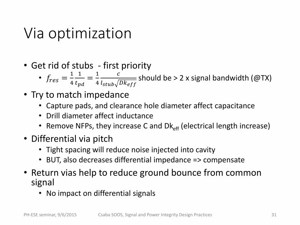
Via optimization
• Get rid of stubs - first priority• 𝑓𝑟𝑒𝑠 =
1
4
1
𝑡𝑝𝑑=
1
4
𝑐
𝑙𝑠𝑡𝑢𝑏 𝐷𝑘𝑒𝑓𝑓should be > 2 x signal bandwidth (@TX)
• Try to match impedance• Capture pads, and clearance hole diameter affect capacitance• Drill diameter affect inductance• Remove NFPs, they increase C and Dkeff (electrical length increase)
• Differential via pitch• Tight spacing will reduce noise injected into cavity• BUT, also decreases differential impedance => compensate
• Return vias help to reduce ground bounce from common signal• No impact on differential signals
PH-ESE seminar, 9/6/2015 Csaba SOOS, Signal and Power Integrity Design Practices 31
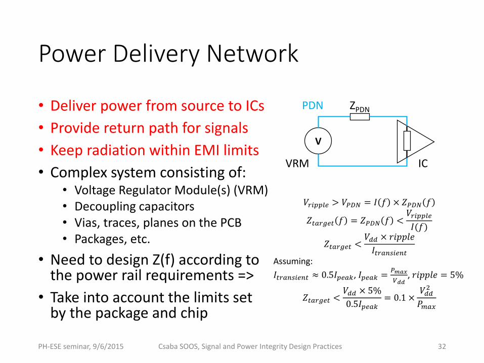
Power Delivery Network
• Deliver power from source to ICs
• Provide return path for signals
• Keep radiation within EMI limits
• Complex system consisting of:• Voltage Regulator Module(s) (VRM)• Decoupling capacitors• Vias, traces, planes on the PCB• Packages, etc.
• Need to design Z(f) according to the power rail requirements =>
• Take into account the limits setby the package and chip
V
ZPDN
IC
PDN
VRM
𝑉𝑟𝑖𝑝𝑝𝑙𝑒 > 𝑉𝑃𝐷𝑁 = 𝐼 𝑓 × 𝑍𝑃𝐷𝑁 𝑓
𝑍𝑡𝑎𝑟𝑔𝑒𝑡 𝑓 = 𝑍𝑃𝐷𝑁 𝑓 <𝑉𝑟𝑖𝑝𝑝𝑙𝑒
𝐼(𝑓)
𝑍𝑡𝑎𝑟𝑔𝑒𝑡 <𝑉𝑑𝑑 × 𝑟𝑖𝑝𝑝𝑙𝑒
𝐼𝑡𝑟𝑎𝑛𝑠𝑖𝑒𝑛𝑡
Assuming:
𝐼𝑡𝑟𝑎𝑛𝑠𝑖𝑒𝑛𝑡 ≈ 0.5𝐼𝑝𝑒𝑎𝑘, 𝐼𝑝𝑒𝑎𝑘 =𝑃𝑚𝑎𝑥
𝑉𝑑𝑑, 𝑟𝑖𝑝𝑝𝑙𝑒 = 5%
𝑍𝑡𝑎𝑟𝑔𝑒𝑡 <𝑉𝑑𝑑 × 5%
0.5𝐼𝑝𝑒𝑎𝑘= 0.1 ×
𝑉𝑑𝑑2
𝑃𝑚𝑎𝑥
PH-ESE seminar, 9/6/2015 Csaba SOOS, Signal and Power Integrity Design Practices 32

PDN design challenge
DC-10kHz 10-100kHz 100kHz-100MHz Beyond 100MHz
On-die Capacitance130nm technology:
130𝑛𝐹
𝑐𝑚2
We can influence this region.
Package inductance:~nH - ~pH
PH-ESE seminar, 9/6/2015 Csaba SOOS, Signal and Power Integrity Design Practices 33
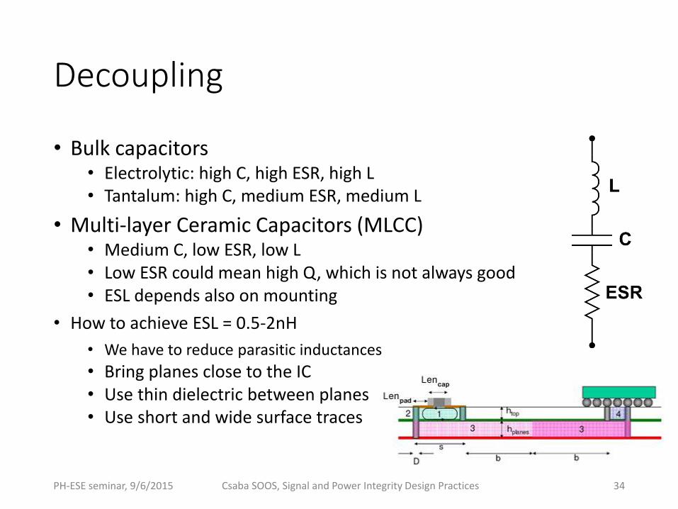
Decoupling
• Bulk capacitors• Electrolytic: high C, high ESR, high L• Tantalum: high C, medium ESR, medium L
• Multi-layer Ceramic Capacitors (MLCC)• Medium C, low ESR, low L• Low ESR could mean high Q, which is not always good• ESL depends also on mounting
• How to achieve ESL = 0.5-2nH
• We have to reduce parasitic inductances
• Bring planes close to the IC• Use thin dielectric between planes• Use short and wide surface traces
PH-ESE seminar, 9/6/2015 Csaba SOOS, Signal and Power Integrity Design Practices 34
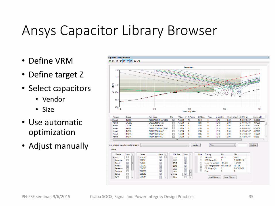
Ansys Capacitor Library Browser
• Define VRM
• Define target Z
• Select capacitors• Vendor
• Size
• Use automaticoptimization
• Adjust manually
PH-ESE seminar, 9/6/2015 Csaba SOOS, Signal and Power Integrity Design Practices 35

Tools
• Impedance calculators• Quick answer but not always accurate, good for estimation
• PCB Saturn, Qucs
• Field solvers• 2D/3D, hybrid
• Slightly more complicated to set up, but accurate
• CERN• ANSYS EM (HFSS, Q3D, Siwave, Designer, Via wizard, PI advisor)
• HyperLynx (not supported)
• Cadence
• Other tools: CST (3D EM solver), Qucs
PH-ESE seminar, 9/6/2015 Csaba SOOS, Signal and Power Integrity Design Practices 36
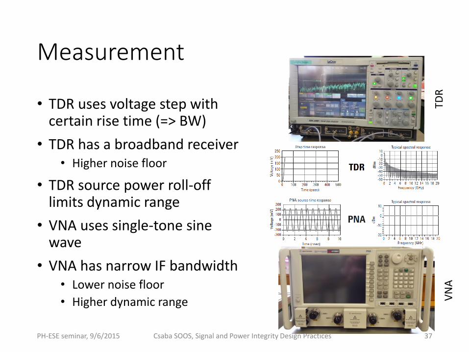
Measurement
• TDR uses voltage step with certain rise time (=> BW)
• TDR has a broadband receiver• Higher noise floor
• TDR source power roll-off limits dynamic range
• VNA uses single-tone sine wave
• VNA has narrow IF bandwidth• Lower noise floor
• Higher dynamic range
TDR
VN
A
PH-ESE seminar, 9/6/2015 Csaba SOOS, Signal and Power Integrity Design Practices 37

TDR vs VNA, dynamic rangeS-parameters (measurement) Eye diagram (simulation, ANSYS)
5Gb/s PRBS-7(PNA)
5Gb/s PRBS-7(TDR)
PH-ESE seminar, 9/6/2015 Csaba SOOS, Signal and Power Integrity Design Practices 38
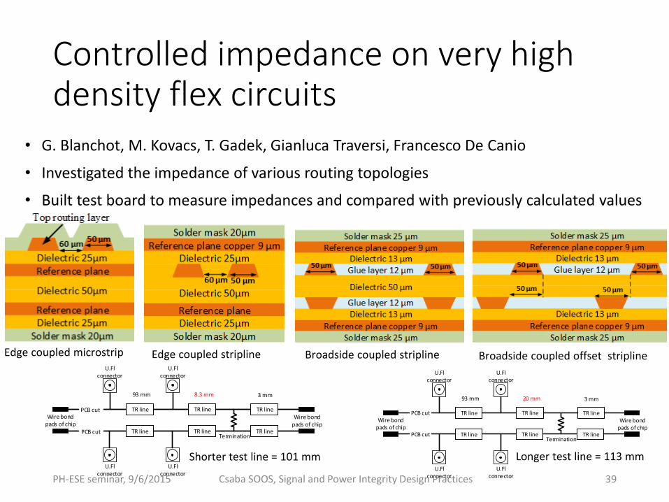
Controlled impedance on very high density flex circuits
• G. Blanchot, M. Kovacs, T. Gadek, Gianluca Traversi, Francesco De Canio
• Investigated the impedance of various routing topologies
• Built test board to measure impedances and compared with previously calculated values
PCB cut TR line TR line TR line
PCB cut TR line TR line TR line
U.Fl connector
U.Fl connector
U.Fl connector
U.Fl connector
93 mm 20 mm 3 mm
Wire bond pads of chip
Wire bond pads of chip
Termination
PCB cut TR line TR line TR line
PCB cut TR line TR line TR line
U.Fl connector
U.Fl connector
U.Fl connector
U.Fl connector
93 mm 8.3 mm 3 mm
Wire bond pads of chip
Wire bond pads of chip
Termination
Edge coupled microstrip Edge coupled stripline Broadside coupled stripline Broadside coupled offset stripline
Shorter test line = 101 mm Longer test line = 113 mm
PH-ESE seminar, 9/6/2015 Csaba SOOS, Signal and Power Integrity Design Practices 39
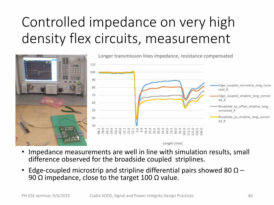
Controlled impedance on very high density flex circuits, measurement
• Impedance measurements are well in line with simulation results, small difference observed for the broadside coupled striplines.
• Edge-coupled microstrip and stripline differential pairs showed 80 Ω –90 Ω impedance, close to the target 100 Ω value.
30
40
50
60
70
80
90
100
110
-88
.1-7
8.6
-69
.1
-59
.6-5
0.1
-40
.6-3
1.1
-21
.6-1
2.1
-2.6
6.9
16
.42
5.9
35
.5
45
.05
4.5
64
.07
3.5
83
.09
2.5
10
2.0
11
1.5
12
1.0
13
0.5
14
0.0
Length [mm]
Longer transmission lines impedance, resistance compensated
Edge_coupled_microstrip_long_corrected_R
Edge_coupled_stripline_long_corrected_R
Broadside_cp_offset_stripline_long_corrected_R
Broadside_cp_stripline_long_corrected_R
PH-ESE seminar, 9/6/2015 Csaba SOOS, Signal and Power Integrity Design Practices 40
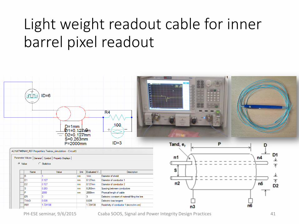
Light weight readout cable for inner barrel pixel readout
PH-ESE seminar, 9/6/2015 Csaba SOOS, Signal and Power Integrity Design Practices 41

Light weight readout cable for inner barrel pixel readout, S parameters
PH-ESE seminar, 9/6/2015 Csaba SOOS, Signal and Power Integrity Design Practices 42
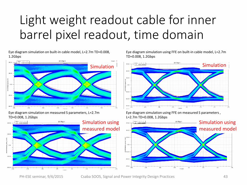
Light weight readout cable for inner barrel pixel readout, time domain
Eye diagram simulation using FFE on built-in cable model, L=2.7m TD=0.008, 1.2Gbps
Eye diagram simulation on measured S parameters, L=2.7m TD=0.008, 1.2Gbps
Eye diagram simulation on built-in cable model, L=2.7m TD=0.008, 1.2Gbps
Eye diagram simulation using FFE on measured S parameters , L=2.7m TD=0.008, 1.2Gbps
Simulation
Simulation usingmeasured model
Simulation
Simulation usingmeasured model
PH-ESE seminar, 9/6/2015 Csaba SOOS, Signal and Power Integrity Design Practices 43
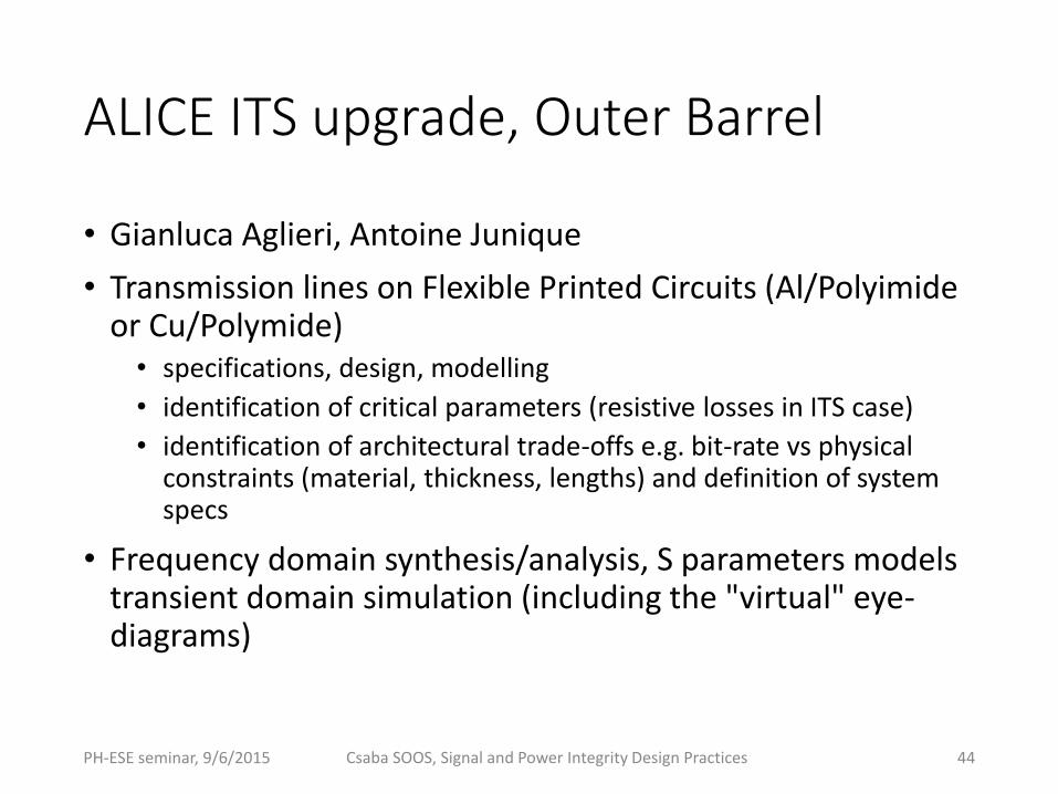
ALICE ITS upgrade, Outer Barrel
• Gianluca Aglieri, Antoine Junique
• Transmission lines on Flexible Printed Circuits (Al/Polyimide or Cu/Polymide)• specifications, design, modelling
• identification of critical parameters (resistive losses in ITS case)
• identification of architectural trade-offs e.g. bit-rate vs physical constraints (material, thickness, lengths) and definition of system specs
• Frequency domain synthesis/analysis, S parameters models transient domain simulation (including the "virtual" eye-diagrams)
PH-ESE seminar, 9/6/2015 Csaba SOOS, Signal and Power Integrity Design Practices 44
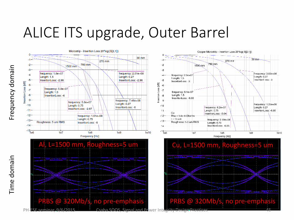
ALICE ITS upgrade, Outer Barrel
Cu, L=1500 mm, Roughness=5 umAl, L=1500 mm, Roughness=5 um
PRBS @ 320Mb/s, no pre-emphasis PRBS @ 320Mb/s, no pre-emphasis
Freq
ue
ncy
do
mai
nTi
me
do
mai
n
PH-ESE seminar, 9/6/2015 Csaba SOOS, Signal and Power Integrity Design Practices 45
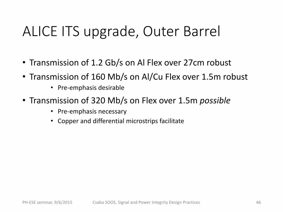
ALICE ITS upgrade, Outer Barrel
• Transmission of 1.2 Gb/s on Al Flex over 27cm robust
• Transmission of 160 Mb/s on Al/Cu Flex over 1.5m robust• Pre-emphasis desirable
• Transmission of 320 Mb/s on Flex over 1.5m possible• Pre-emphasis necessary
• Copper and differential microstrips facilitate
PH-ESE seminar, 9/6/2015 Csaba SOOS, Signal and Power Integrity Design Practices 46

GBTx test board PDN
• 4-port sensing (Kelvin method) for measuring low impedance (plane)
• Simulation carried out using AnsysSIwave
• Nice match above 1 MHz
• Mismatch at low frequency could bedue to capacitor model
David Porret
PH-ESE seminar, 9/6/2015 Csaba SOOS, Signal and Power Integrity Design Practices 47

PCIe40 PDN, current density
Current density too high
Reshaping and splitting planes toreduce current
Jean-Pierre Cachemiche, Fred Rethore (CPPM)Cadence Sigrity
PH-ESE seminar, 9/6/2015 Csaba SOOS, Signal and Power Integrity Design Practices 48

PCIe40 PDN, IR drop
VCCT (0.9V, 5A) ~ 60mV
VCCR (0.9V, 13A) ~ 160mV
Redesigned shapes to reduce drop
Jean-Pierre Cachemiche, Fred Rethore (CPPM)Cadence Sigrity
VCCT (0.9V, 5A) ~ 15mV
VCCR (0.9V, 13A) ~ 50mV
PH-ESE seminar, 9/6/2015 Csaba SOOS, Signal and Power Integrity Design Practices 49

PH-ESE seminar, 9/6/2015 Csaba SOOS, Signal and Power Integrity Design Practices 50

Backup slides
PH-ESE seminar, 9/6/2015Csaba SOOS, Signal and Power Integrity Design
Practices51

PDN analysis, mounting inductance
Capacitor Model Mounting Quality Total Mounting
Inductance, nH
Estimated ESL,
nH
Actual Resonance
Frequency, MHz
Resonance
Frequency w/o
Mounting, MHz
C6 C=0.1uF, ESL=Auto, ESR=25mOhms good 1.52 0.31 12.89 27.71
C10 C=0.1uF, ESL=Auto, ESR=25mOhms good 0.63 0.28 19.98 27.71
BottomTop
Bottom
Top
PH-ESE seminar, 9/6/2015 Csaba SOOS, Signal and Power Integrity Design Practices 52
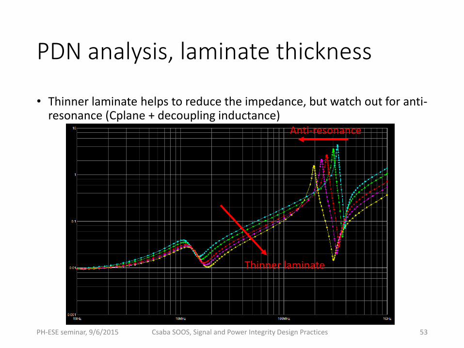
PDN analysis, laminate thickness
• Thinner laminate helps to reduce the impedance, but watch out for anti-resonance (Cplane + decoupling inductance)
Thinner laminate
Anti-resonance
PH-ESE seminar, 9/6/2015 Csaba SOOS, Signal and Power Integrity Design Practices 53

Unwanted coupling seen on S21
Design File: S_params_coupled_resonator
HyperLynx LineSim v8.2.1
TL1
50.7 ohms298.538 ps5.000 cmCoupled Stackup
N1 N2
TL2
60.2 ohms296.567 ps5.000 cmCoupled Stackup
R1
1.0 M ohms
R2
1.0 M ohms
PH-ESE seminar, 9/6/2015 Csaba SOOS, Signal and Power Integrity Design Practices 54
HyperLynx, PCIe Gen3 channel
Design File: Kintex7_IBIS_AMI_PCIe_channel
HyperLynx LineSim v8.2.1
J3
PCIeGen3_14in_...
Port1 Port2
Port3 Port4
J1
Xilinx_7k325t_ff...
Port1
Port2
Port3
Port4
U2
xilinx_7gtx_txxilinx_7gtx_tx
1n
1p
J2
Xilinx_7k325t_ff...
Port1
Port2
Port3
Port4
U3
xilinx_k7_gtx_ami_rxrx_n
2p
2n
PH-ESE seminar, 9/6/2015 Csaba SOOS, Signal and Power Integrity Design Practices 55