SiGe HBT BiCMOS Field Programmable Gate Arrays for Fast Reconfigurable Computing
61
SiGe HBT BiCMOS Field Programmable Gate Arrays for Fast Reconfigurable Computing Bryan S. Goda Rensselaer Polytechnic Institute Troy, New York
-
Upload
austin-barry -
Category
Documents
-
view
63 -
download
4
description
SiGe HBT BiCMOS Field Programmable Gate Arrays for Fast Reconfigurable Computing. Bryan S. Goda Rensselaer Polytechnic Institute Troy, New York. Agenda. Introduction BiCMOS FPGA History SiGe HBT BiCMOS Process Current Mode Logic Xilinx 6200 FPGA Design Configuration Memory - PowerPoint PPT Presentation
Transcript of SiGe HBT BiCMOS Field Programmable Gate Arrays for Fast Reconfigurable Computing
SiGe HBT BiCMOS Field Programmable Gate Arrays for
Fast Reconfigurable Computing
Bryan S. Goda
Rensselaer Polytechnic Institute
Troy, New York
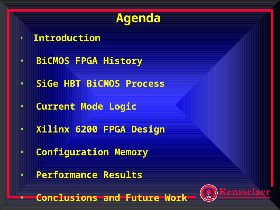
Agenda
• Introduction
• BiCMOS FPGA History
• SiGe HBT BiCMOS Process
• Current Mode Logic
• Xilinx 6200 FPGA Design
• Configuration Memory
• Performance Results
• Conclusions and Future Work
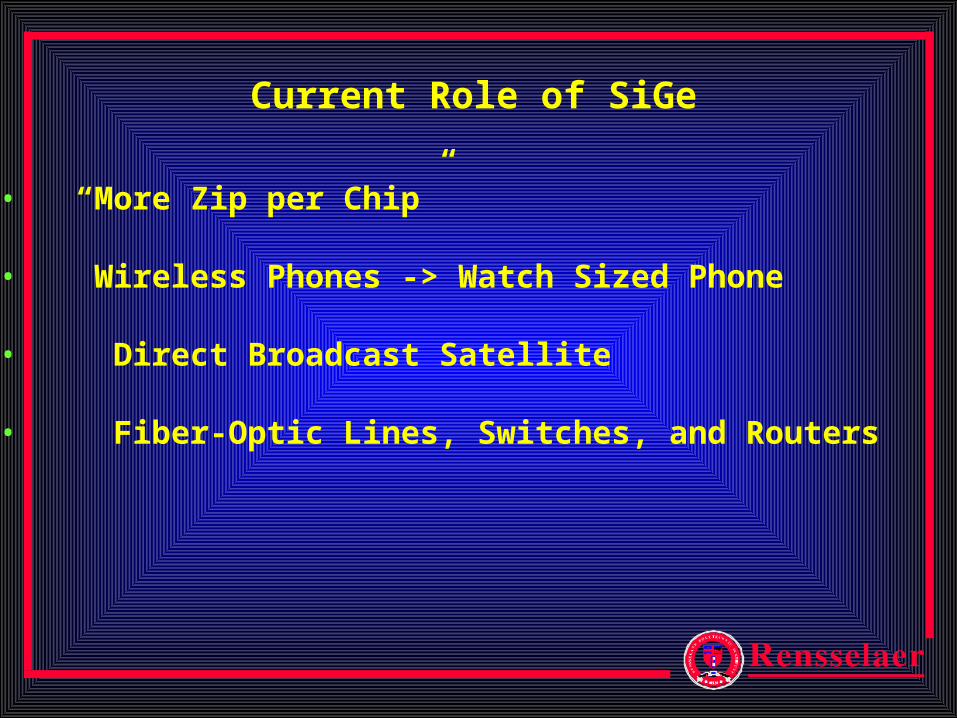
Current Role of SiGe
• “More Zip per Chip”
• Wireless Phones -> Watch Sized Phone
• Direct Broadcast Satellite
• Fiber-Optic Lines, Switches, and Routers
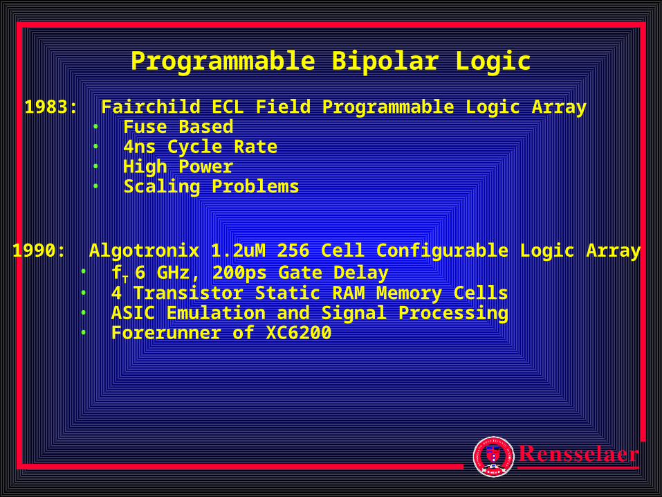
Programmable Bipolar Logic
1983: Fairchild ECL Field Programmable Logic Array• Fuse Based• 4ns Cycle Rate• High Power• Scaling Problems
1990: Algotronix 1.2uM 256 Cell Configurable Logic Array• fT 6 GHz, 200ps Gate Delay• 4 Transistor Static RAM Memory Cells• ASIC Emulation and Signal Processing• Forerunner of XC6200
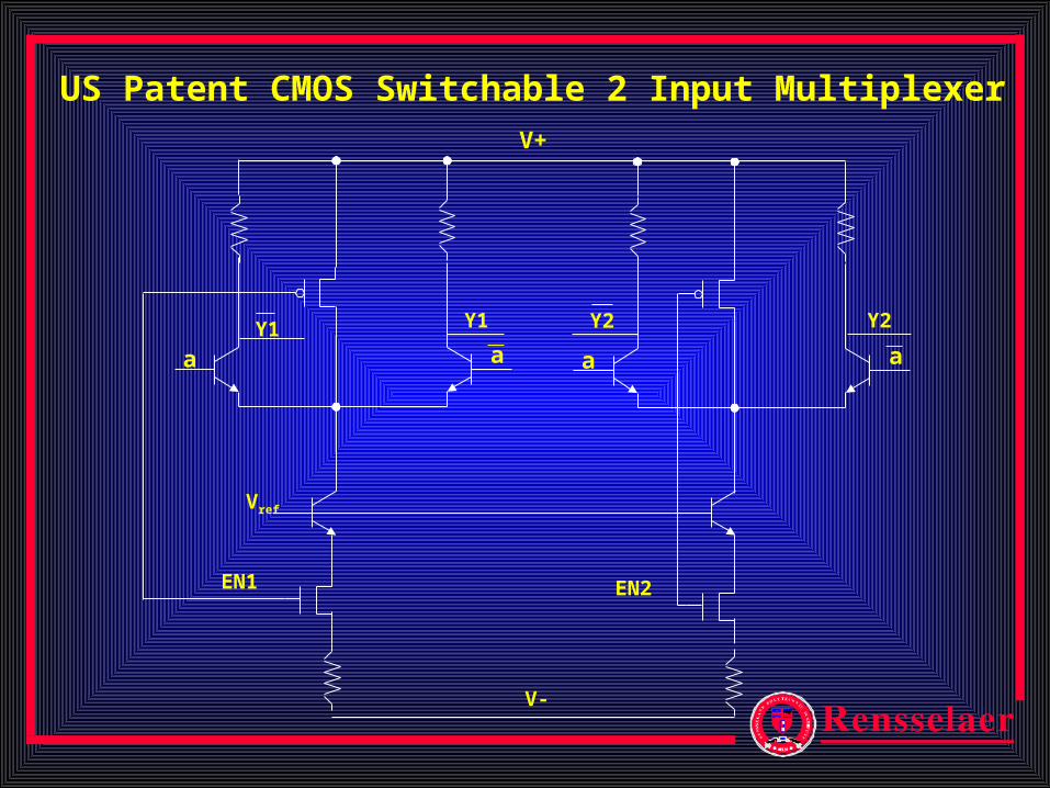
V+
a a
Vref
a a
EN1 EN2
V-
Y1 Y1 Y2 Y2
US Patent CMOS Switchable 2 Input Multiplexer
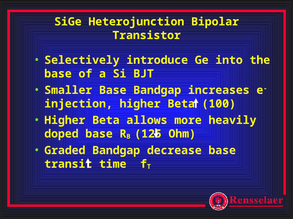
SiGe Heterojunction Bipolar Transistor
• Selectively introduce Ge into the base of a Si BJT
• Smaller Base Bandgap increases e- injection, higher Beta (100)
• Higher Beta allows more heavily doped base RB (125 Ohm)
• Graded Bandgap decrease base transit time fT
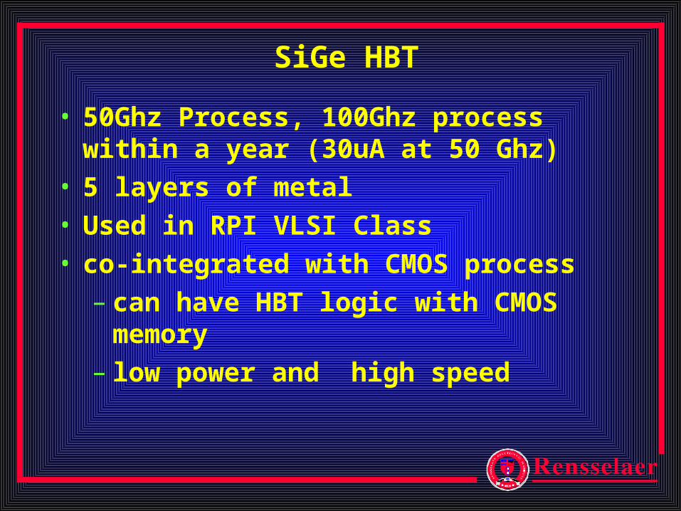
SiGe HBT
• 50Ghz Process, 100Ghz process within a year (30uA at 50 Ghz)
• 5 layers of metal• Used in RPI VLSI Class• co-integrated with CMOS process
– can have HBT logic with CMOS memory– low power and high speed
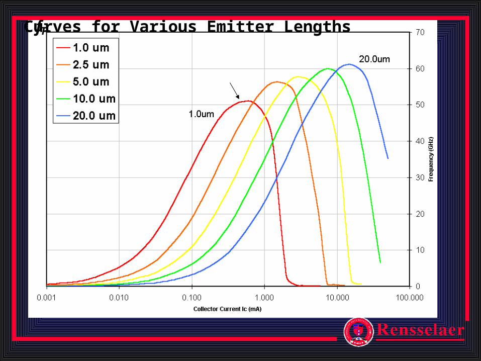
fT Curves for Various Emitter Lengths
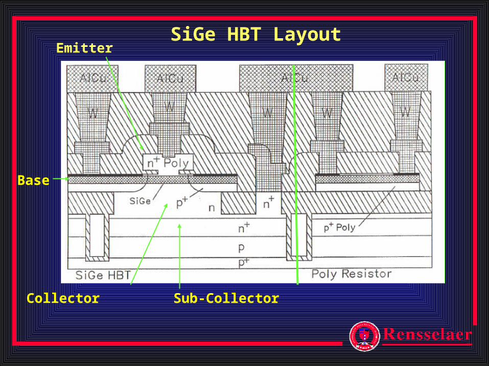
SiGe HBT Layout
Base
Emitter
Collector Sub-Collector
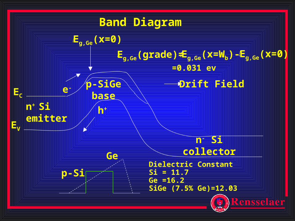
EC
EV
e-
h+n+ Siemitter
p-Si
Ge
p-SiGebase
Eg,Ge(x=0)
Eg,Ge(grade)= Eg,Ge(x=Wb)- Eg,Ge(x=0)
Drift Field
n- Sicollector
Band Diagram
=0.031 ev
Dielectric ConstantSi = 11.7Ge =16.2SiGe (7.5% Ge)=12.03
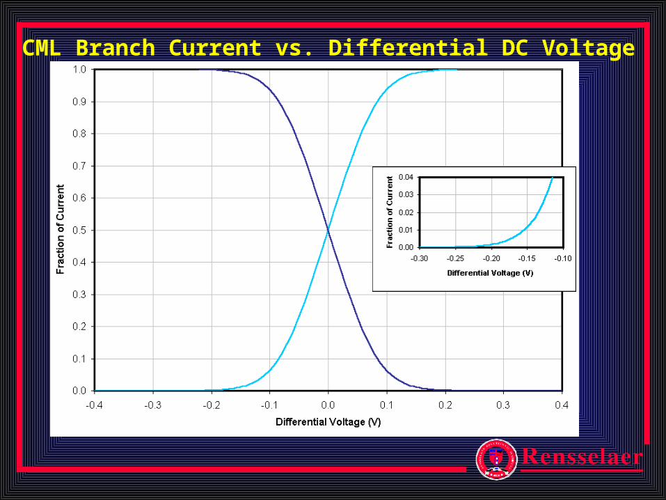
CML Branch Current vs. Differential DC Voltage
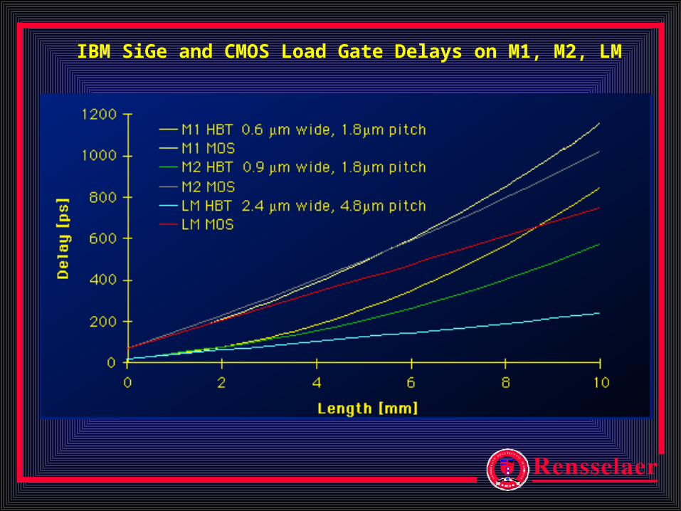
IBM SiGe and CMOS Load Gate Delays on M1, M2, LM
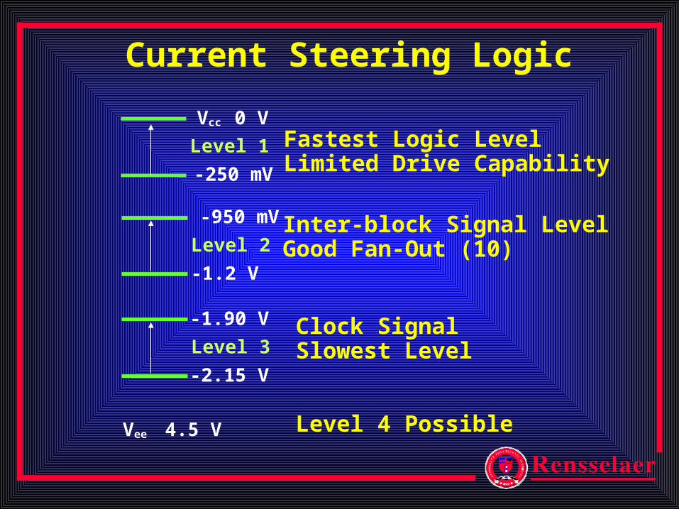
Current Steering Logic
Level 1
Vcc 0 V
-250 mV
Level 2
-950 mV
-1.2 V
Level 3
-1.90 V
-2.15 V
Vee 4.5 V
Fastest Logic LevelLimited Drive Capability
Inter-block Signal LevelGood Fan-Out (10)
Clock SignalSlowest Level
Level 4 Possible
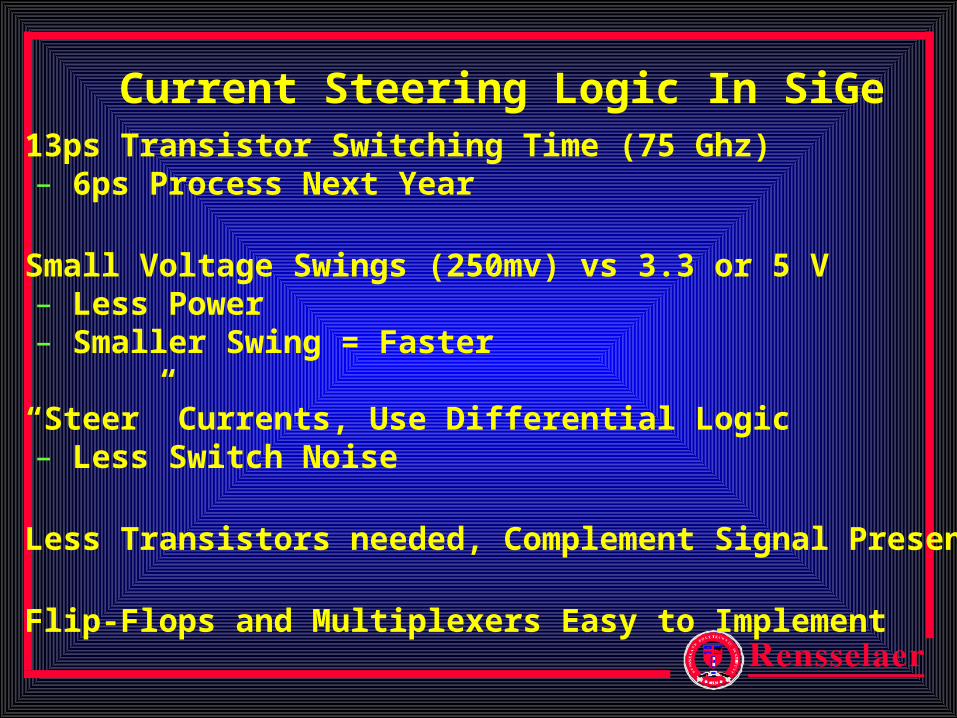
Current Steering Logic In SiGe• 13ps Transistor Switching Time (75 Ghz)
– 6ps Process Next Year
• Small Voltage Swings (250mv) vs 3.3 or 5 V– Less Power– Smaller Swing = Faster
• “Steer” Currents, Use Differential Logic– Less Switch Noise
• Less Transistors needed, Complement Signal Present
• Flip-Flops and Multiplexers Easy to Implement
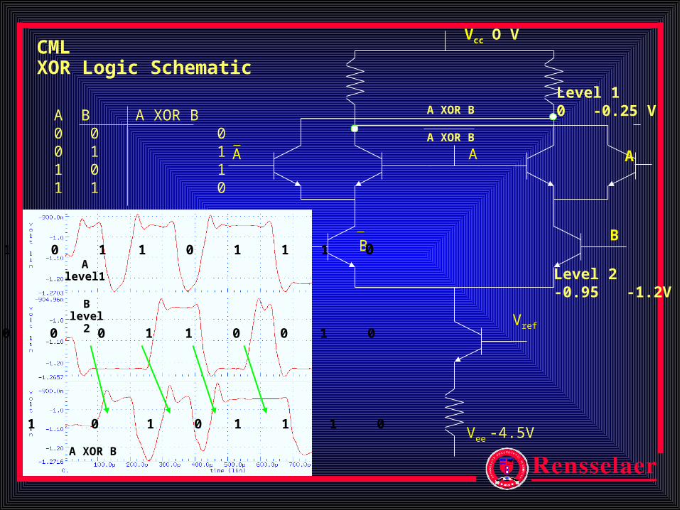
Vcc
AA A
BB
Vee
Vref
A XOR B
A XOR B
O V
Level 10 -0.25 V
Level 2-0.95 -1.2V
-4.5V
A B A XOR B0 0 00 1 11 0 11 1 0
CMLXOR Logic Schematic
1 0 1 1 0 1 1 1 0
0 0 0 1 1 0 0 1 0
1 0 1 0 1 1 1 0
Alevel1
Blevel 2
A XOR B
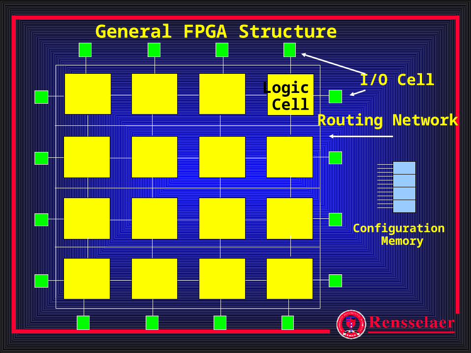
Logic Cell
General FPGA Structure
I/O Cell
Routing Network
Configuration Memory
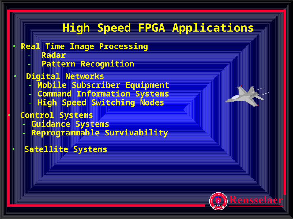
High Speed FPGA Applications
• Real Time Image Processing- Radar- Pattern Recognition
• Digital Networks- Mobile Subscriber Equipment- Command Information Systems- High Speed Switching Nodes
• Control Systems- Guidance Systems- Reprogrammable Survivability
• Satellite Systems

Desired Image
Search Image
1. Desired Image is programmed into chip (1 pixel = 1CLB)2. Load a section of search image3. If enough pixels match, then turn found bit on4. Load another section, or reprogram with new desired image
Image Correlation
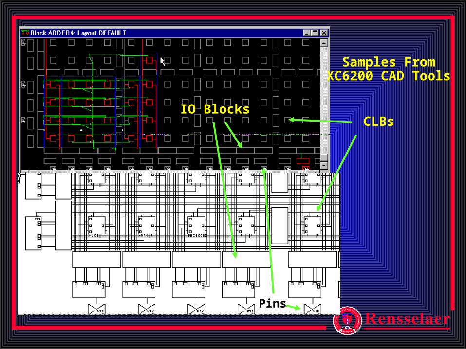
Samples FromXC6200 CAD Tools
CLBsIO Blocks
Pins
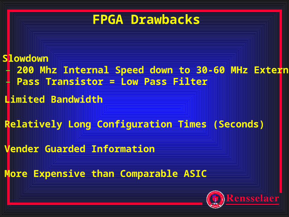
FPGA Drawbacks
• Slowdown – 200 Mhz Internal Speed down to 30-60 MHz External – Pass Transistor = Low Pass Filter
• Limited Bandwidth
• Relatively Long Configuration Times (Seconds)
• Vender Guarded Information
• More Expensive than Comparable ASIC
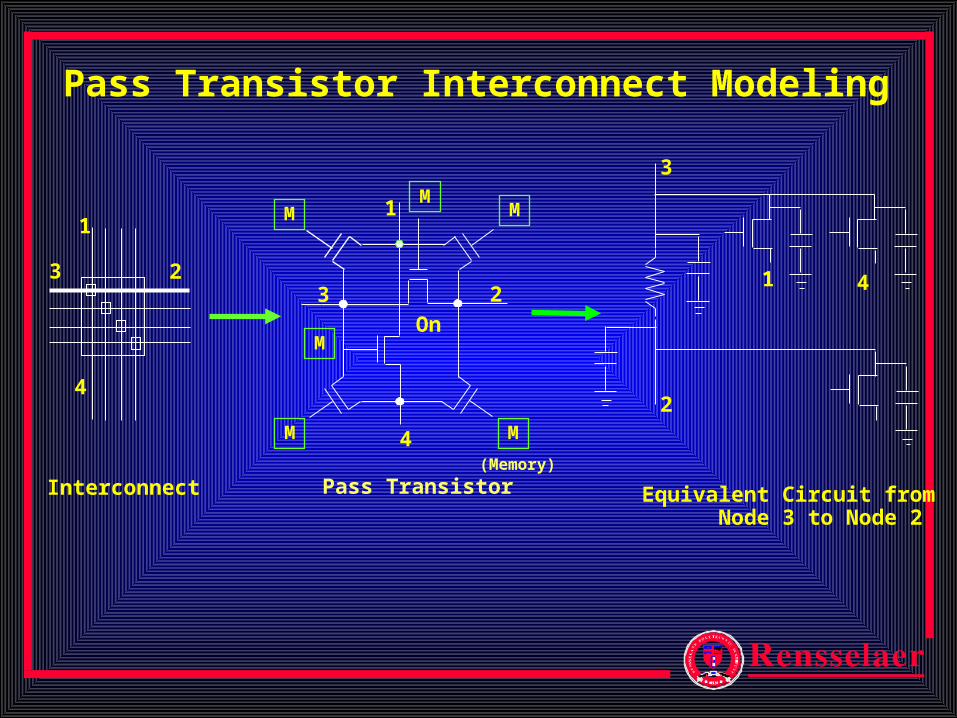
Equivalent Circuit from Node 3 to Node 2
M
M
M M
MM
1
On
23
4
3
2
1 4
Interconnect
4
1
23
Pass Transistor (Memory)
Pass Transistor Interconnect Modeling
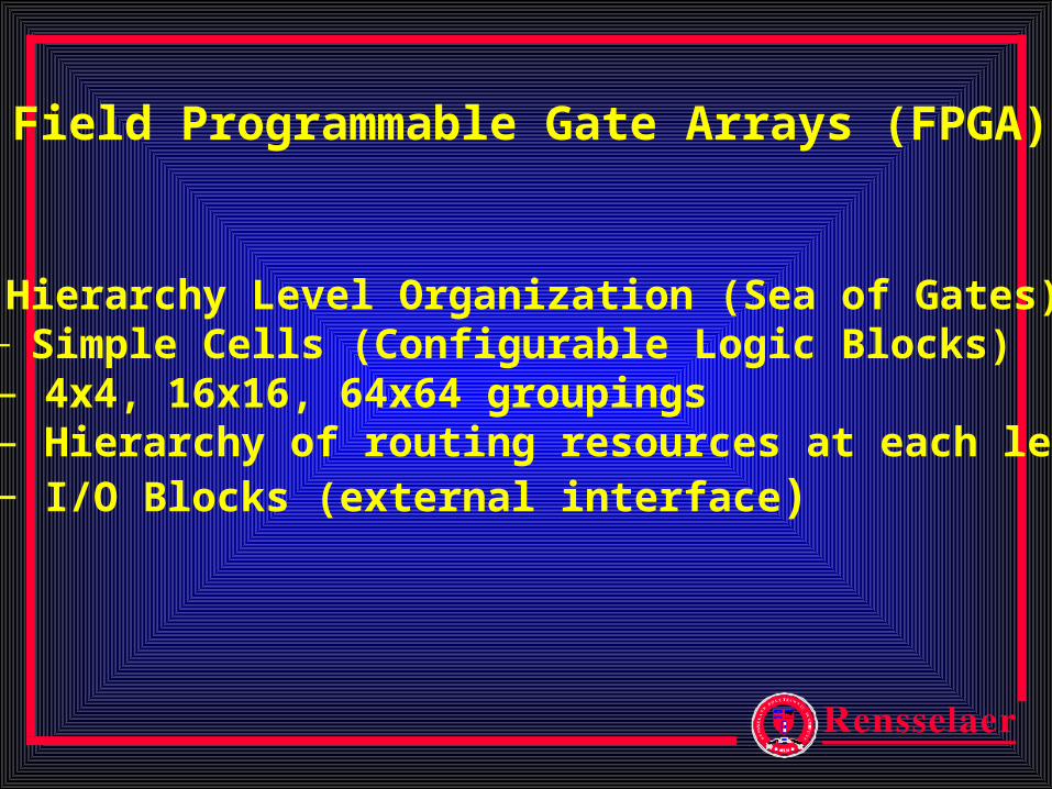
Field Programmable Gate Arrays (FPGA)
• Hierarchy Level Organization (Sea of Gates)– Simple Cells (Configurable Logic Blocks)– 4x4, 16x16, 64x64 groupings– Hierarchy of routing resources at each level– I/O Blocks (external interface)
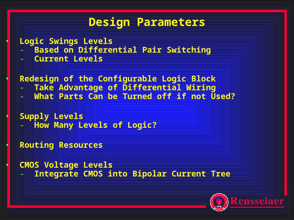
Design Parameters
• Logic Swings Levels- Based on Differential Pair Switching- Current Levels
• Redesign of the Configurable Logic Block- Take Advantage of Differential Wiring- What Parts Can be Turned off if not Used?
• Supply Levels- How Many Levels of Logic?
• Routing Resources
• CMOS Voltage Levels- Integrate CMOS into Bipolar Current Tree
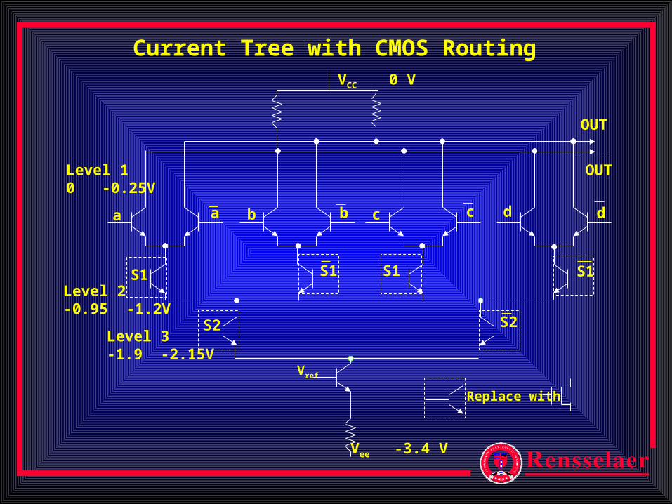
a
VCC 0 V
OUT
OUT
a b b c c d d
S1 S1 S1 S1
S2 S2
Vee -3.4 V
Level 3-1.9 -2.15V
Level 2-0.95 -1.2V
Level 10 -0.25V
Replace with
Vref
Current Tree with CMOS Routing
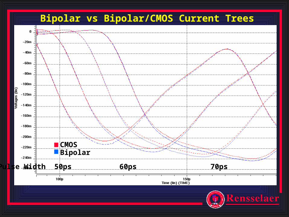
Pulse Width 50ps 60ps 70ps 100ps
CMOSBipolar
Bipolar vs Bipolar/CMOS Current Trees
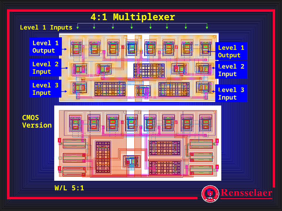
4:1 MultiplexerLevel 1 Inputs
Level 1Output
Level 1Output
Level 2Input
Level 2Input
Level 3Input Level 3
Input
CMOSVersion
W/L 5:1
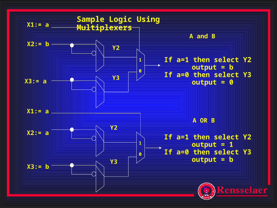
If a=1 then select Y2output = b
If a=0 then select Y3output = 0
A OR B
A and B
If a=1 then select Y2output = 1
If a=0 then select Y3output = b
X2:= a
1
0
X1:= a
X3:= b
Y2
Y3
X2:= b
1
0
X1:= a
X3:= a
Y2
Y3
Sample Logic Using Multiplexers
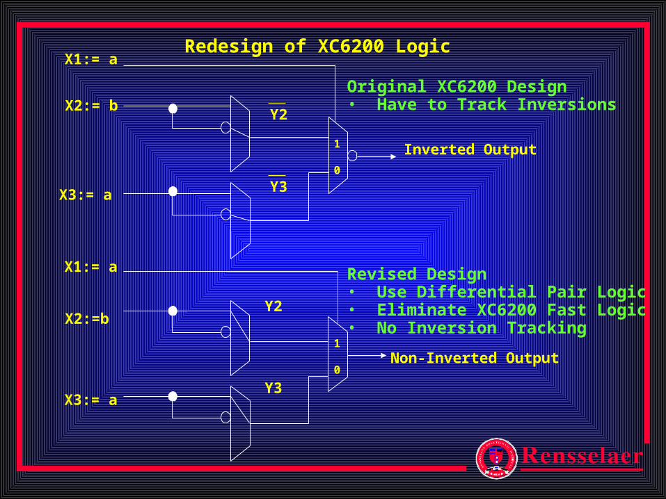
Non-Inverted Output
Inverted Output
X2:=b
1
0
X1:= a
X3:= a
Y2
Y3
X2:= b
1
0
X1:= a
X3:= a
Y2
Y3
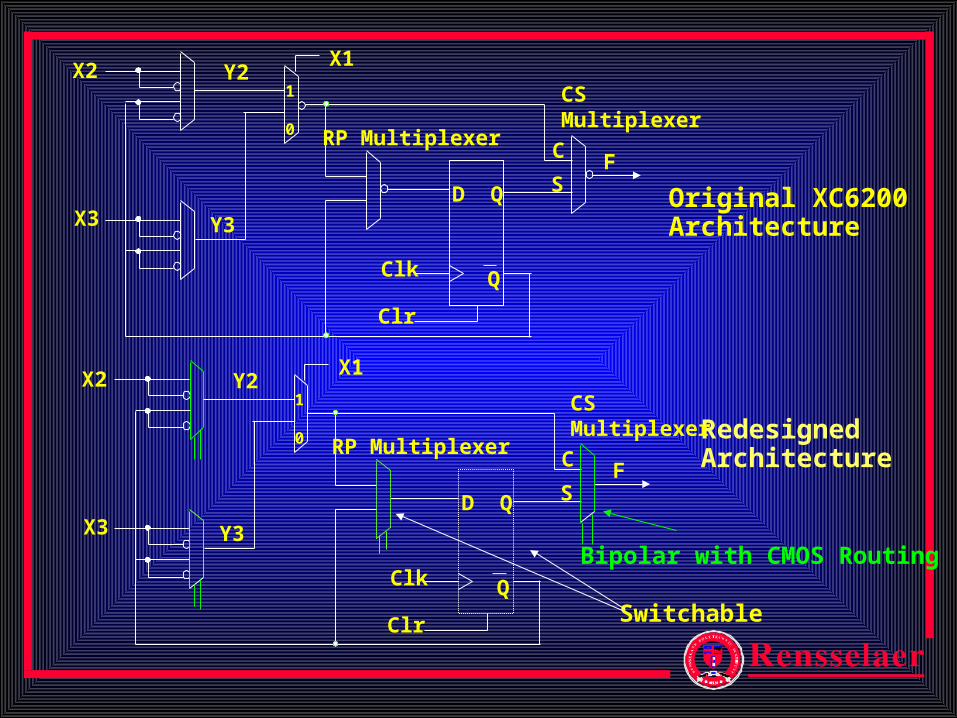
Redesign of XC6200 Logic
Original XC6200 Design• Have to Track Inversions
Revised Design• Use Differential Pair Logic• Eliminate XC6200 Fast Logic• No Inversion Tracking
X1Y2X2
X3 Y3
1
0
D Q
Clk Q
FC
S
RP Multiplexer
CS Multiplexer
Clr
Original XC6200Architecture
RedesignedArchitecture
X1Y2X2
X3 Y3
1
0
D Q
Clk Q
FC
S
RP Multiplexer
CS Multiplexer
Clr Switchable
Bipolar with CMOS Routing
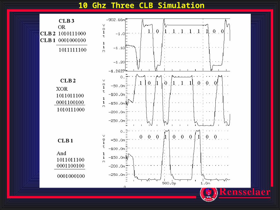
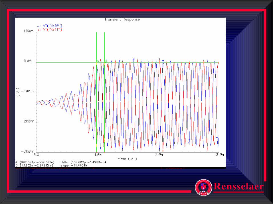
10 Ghz Three CLB Simulation
4:1 MuxHigh Speed Logic
2:1 MuxCMOS Control Buffer
4:1 Mux (off switchable)CMOS Control Master/Slave Latch (off switchable)
(off switchable)
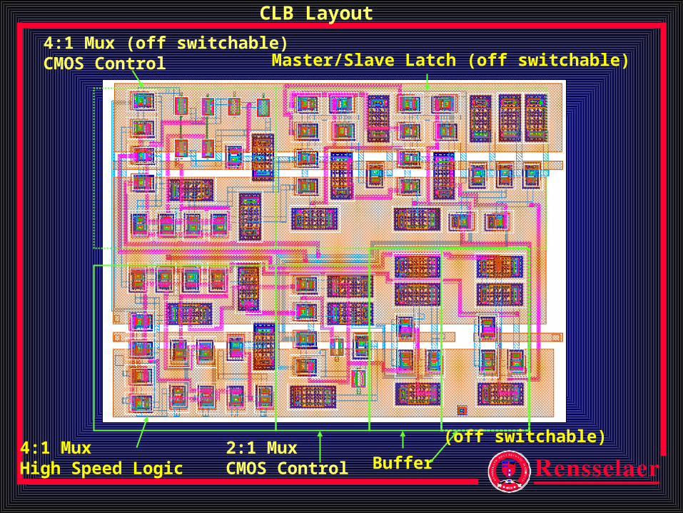
CLB Layout
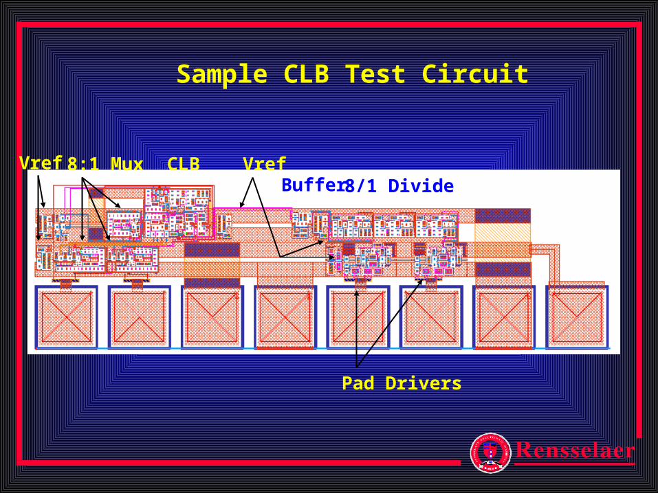
Sample CLB Test Circuit
CLB8:1 Mux
Pad Drivers
8/1 DivideBufferVrefVref
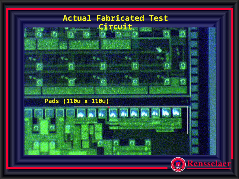
Actual Fabricated Test Circuit
Pads (110u x 110u)
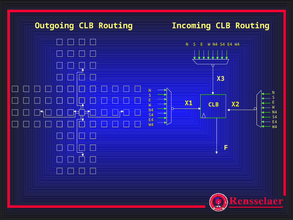
NSEWN4S4E4W4
NSEWN4S4E4W4
F
N S E W N4 S4 E4 W4
X1 X2CLB
X3
Outgoing CLB Routing Incoming CLB Routing
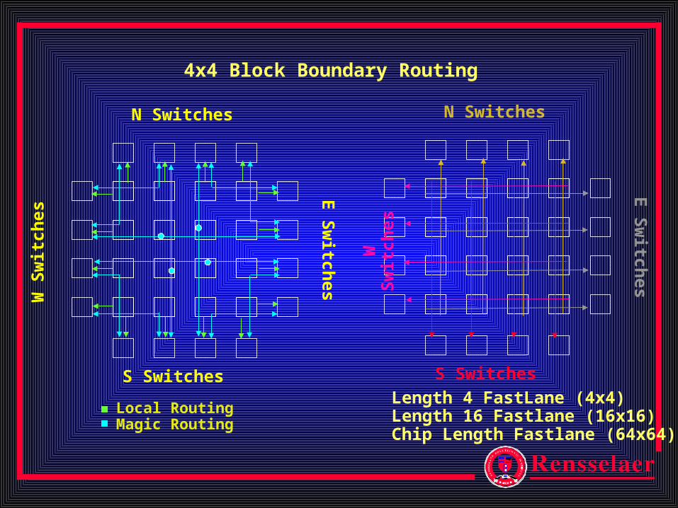
4x4 Block Boundary Routing
S Switches
E S
witch
es
N Switches
W S
wit
ches
S Switches
E S
witch
es
N Switches
W S
wit
ches
Local RoutingMagic Routing
Length 4 FastLane (4x4)Length 16 Fastlane (16x16)Chip Length Fastlane (64x64)
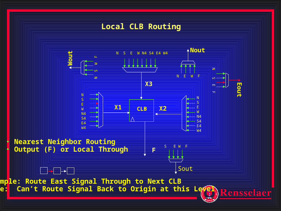
NSEWN4S4E4W4
NSEWN4S4E4W4
F
N S E W N4 S4 E4 W4
X1 X2CLB
X3
Local CLB Routing
N S
W FW
out
S E W F
Sout
N S E
F
Eou
t
N E W F
Nout
• Nearest Neighbor Routing• Output (F) or Local Through
Example: Route East Signal Through to Next CLBNote: Can’t Route Signal Back to Origin at this Level
New
Co
nfi
gu
rati
on
Dat
a
VEE
VEE
VSS VSS
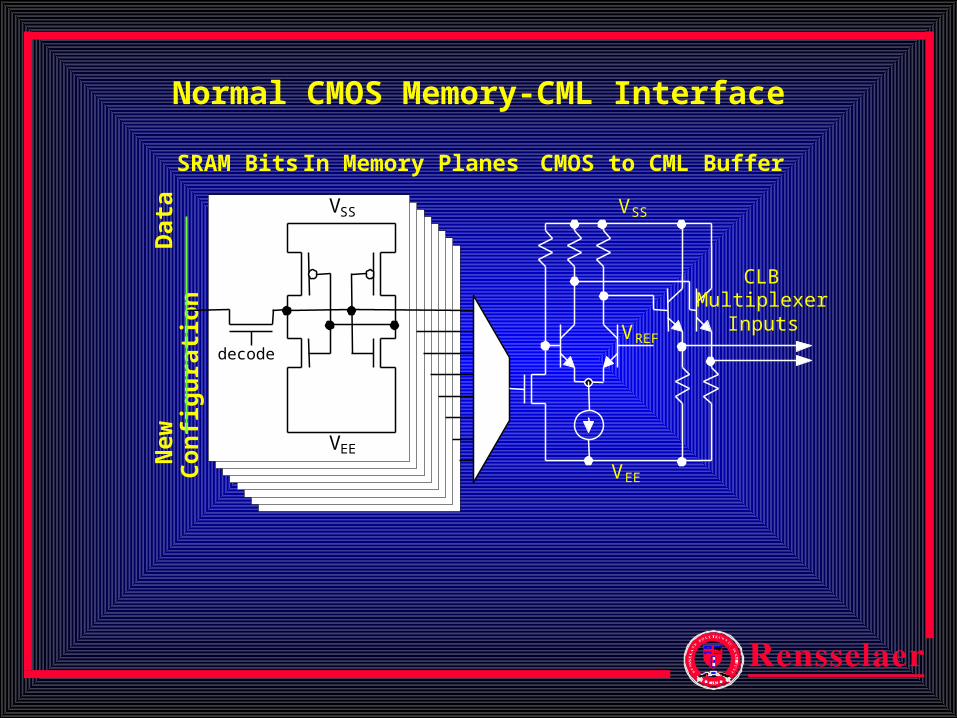
SRAM Bits In Memory Planes CMOS to CML Buffer
decode
CLBMultiplexer
InputsVREF
Normal CMOS Memory-CML Interface
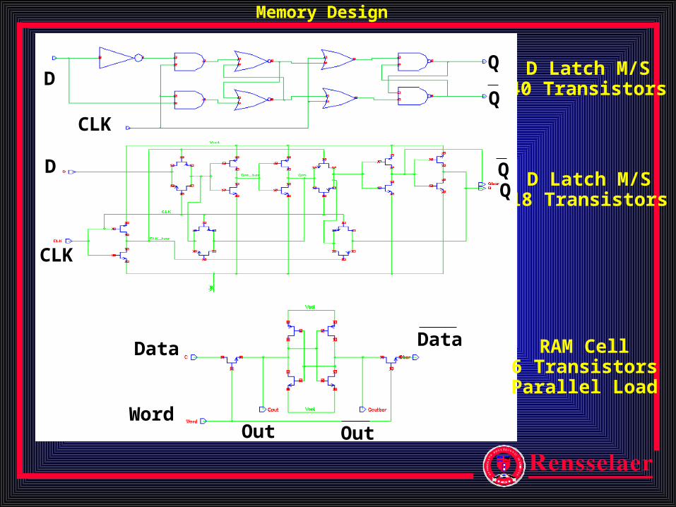
D Latch M/S40 Transistors
D Latch M/S18 Transistors
DQ
Clock
QCLK
D
CLK
Data Data
WordOut Out
RAM Cell6 TransistorsParallel Load
Memory Design
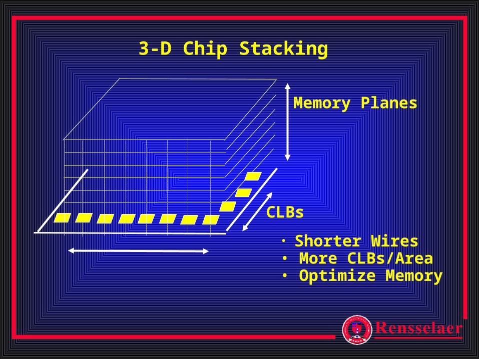
Memory Planes
CLBs
3-D Chip Stacking
• Shorter Wires• More CLBs/Area• Optimize Memory
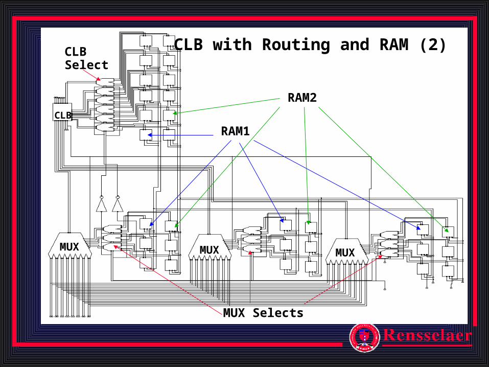
CLB with Routing and RAM (2)
MUX MUX MUX
CLB
MUX Selects
CLBSelect
RAM1
RAM2
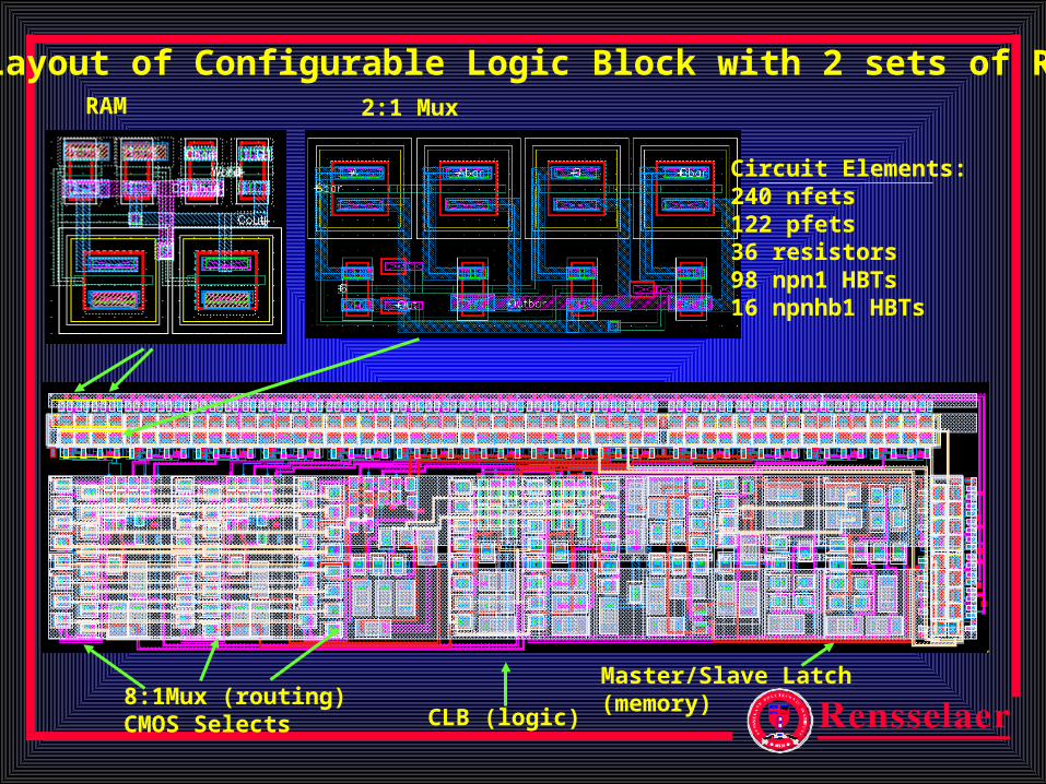
Layout of Configurable Logic Block with 2 sets of RAMRAM 2:1 Mux
8:1Mux (routing)CMOS Selects CLB (logic)
Master/Slave Latch(memory)
Circuit Elements:240 nfets122 pfets36 resistors98 npn1 HBTs16 npnhb1 HBTs
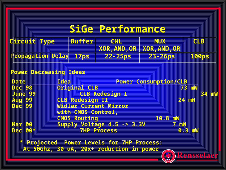
Circuit Type Buffer CMLXOR,AND,OR
MUXXOR,AND,OR
CLB
Propagation Delay 17ps 22-25ps 23-26ps 100ps
SiGe Performance
* Projected Power Levels for 7HP Process:At 50Ghz, 30 uA, 20x+ reduction in power
Power Decreasing Ideas
Date Idea Power Consumption/CLBDec 98 Original CLB 73 mWJune 99 CLB Redesign I 34 mWAug 99 CLB Redesign II 24 mWDec 99 Widlar Current Mirror
with CMOS Control, CMOS Routing 10.8 mW
Mar 00 Supply Voltage 4.5 -> 3.3V 7 mWDec 00* 7HP Process 0.3 mW
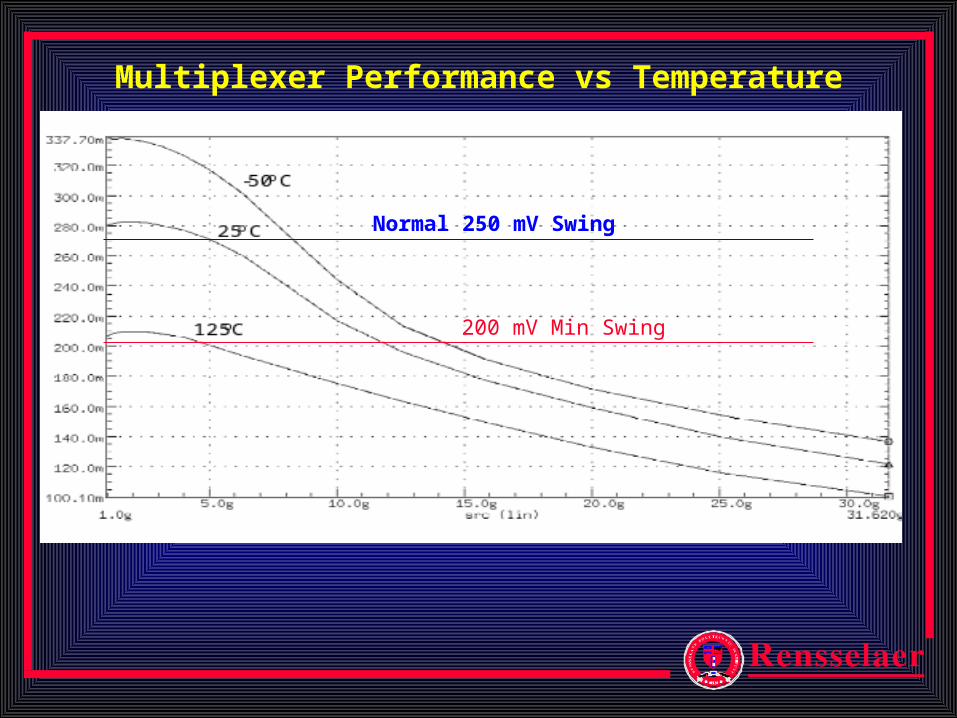
Multiplexer Performance vs Temperature
Normal 250 mV Swing
200 mV Min Swing
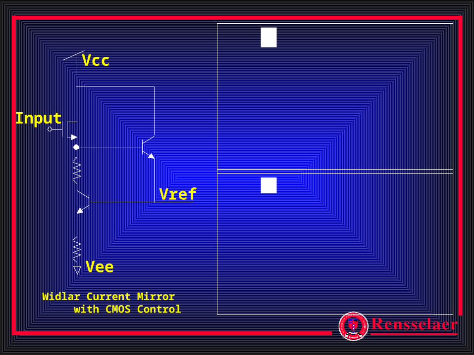
Vcc
Vref
Vee
Input
Widlar Current Mirror with CMOS Control
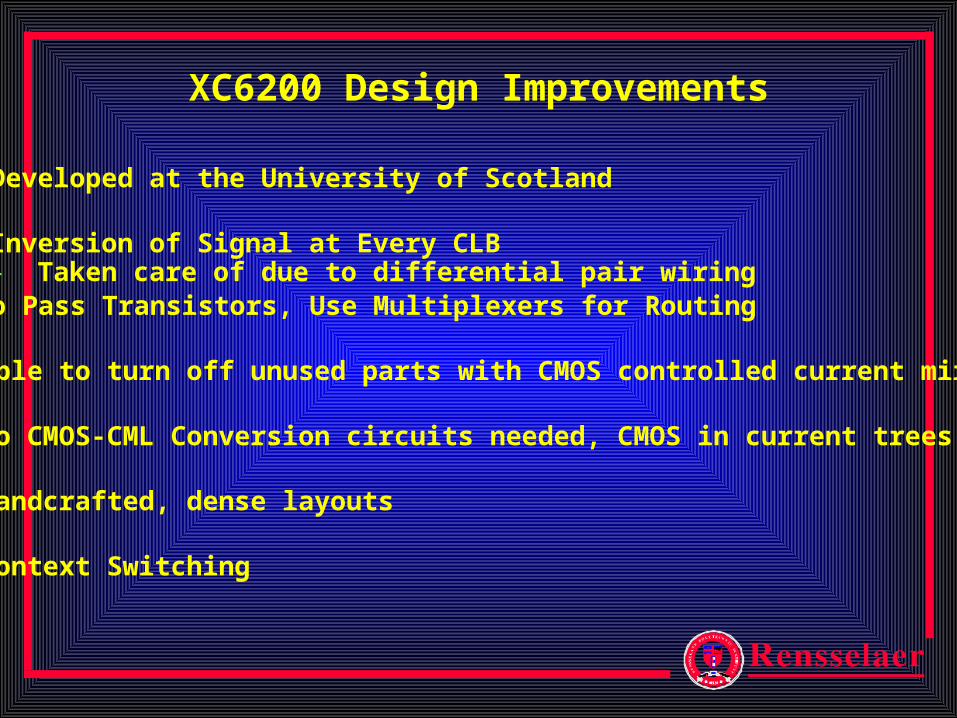
XC6200 Design Improvements
• Developed at the University of Scotland
• Inversion of Signal at Every CLB- Taken care of due to differential pair wiring
• No Pass Transistors, Use Multiplexers for Routing
• Able to turn off unused parts with CMOS controlled current mirror
• No CMOS-CML Conversion circuits needed, CMOS in current trees
• Handcrafted, dense layouts
• Context Switching
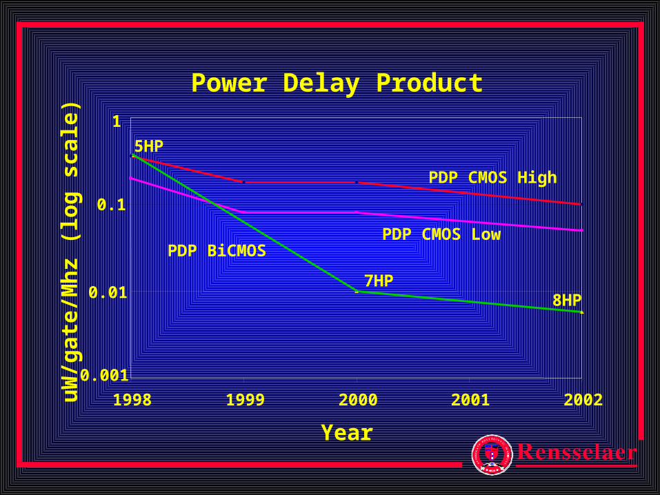
Power Delay Product
0.001
0.01
0.1
1
1998 1999 2000 2001 2002
Year
uW
/gat
e/M
hz
(log
sca
le)
PDP BiCMOS
PDP CMOS High
PDP CMOS Low
5HP
7HP8HP
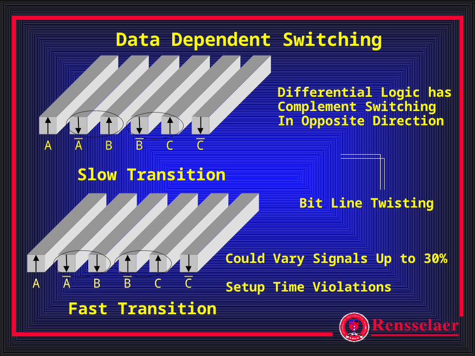
A A B B C C
A A B B C C
Slow Transition
Fast Transition
Data Dependent Switching
Could Vary Signals Up to 30%
Setup Time Violations
Differential Logic hasComplement Switching In Opposite Direction
Bit Line Twisting
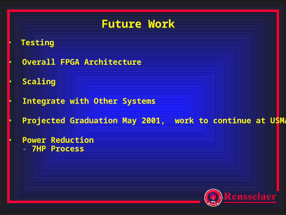
Future Work
• Testing
• Overall FPGA Architecture
• Scaling
• Integrate with Other Systems
• Projected Graduation May 2001, work to continue at USMA
• Power Reduction- 7HP Process
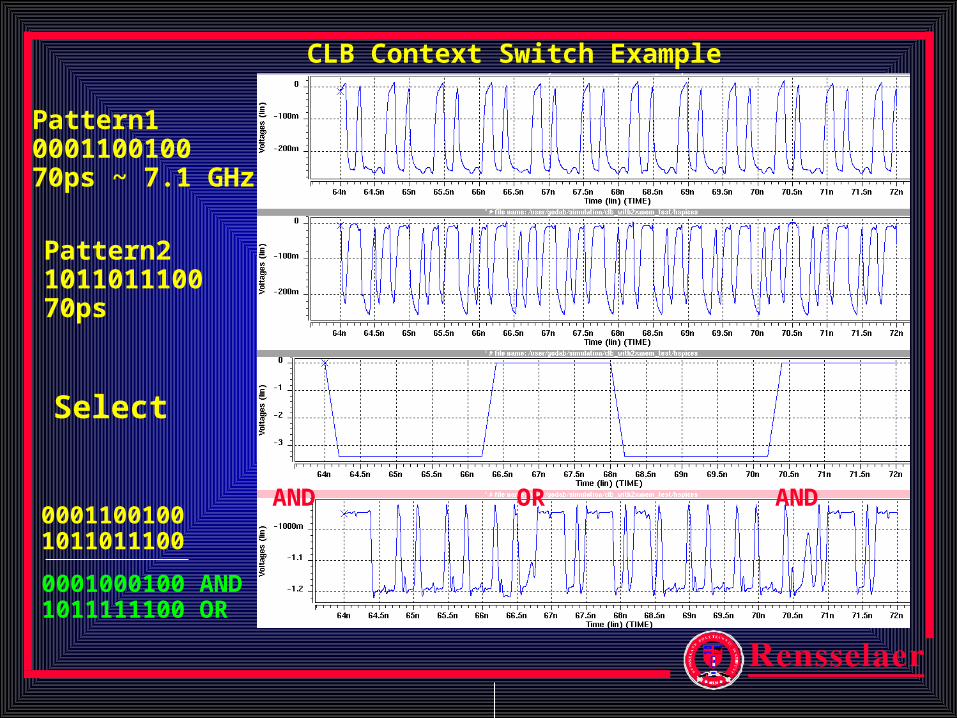
Pattern1000110010070ps ~ 7.1 GHz
Pattern2101101110070ps
Select
00011001001011011100
0001000100 AND1011111100 OR
AND OR AND OR
CLB Context Switch Example
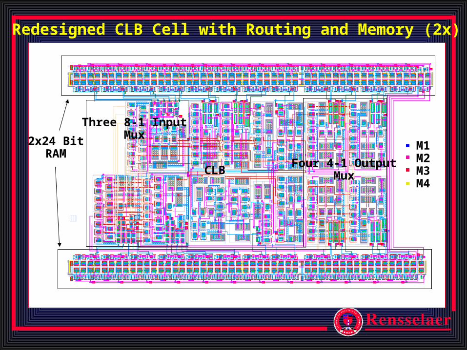
Redesigned CLB Cell with Routing and Memory (2x)
2x24 BitRAM
Three 8-1 InputMux
CLBFour 4-1 Output
Mux
M1M2M3M4
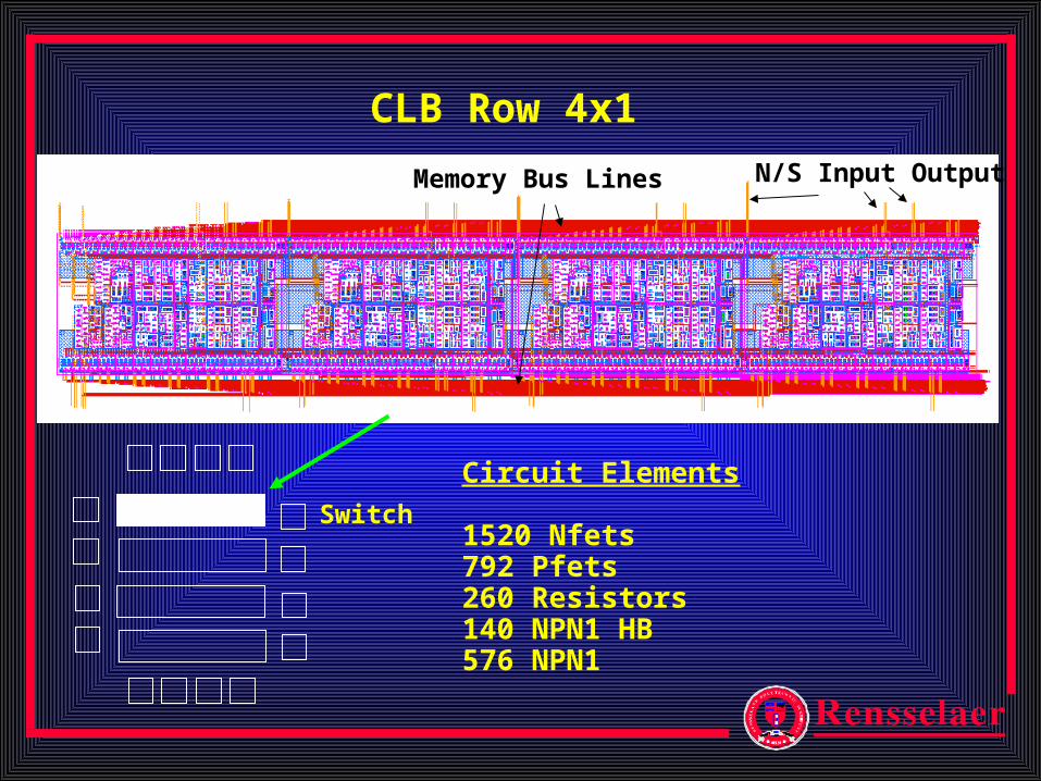
CLB Row 4x1
Switch
Circuit Elements
1520 Nfets792 Pfets260 Resistors140 NPN1 HB576 NPN1
Memory Bus Lines N/S Input Output
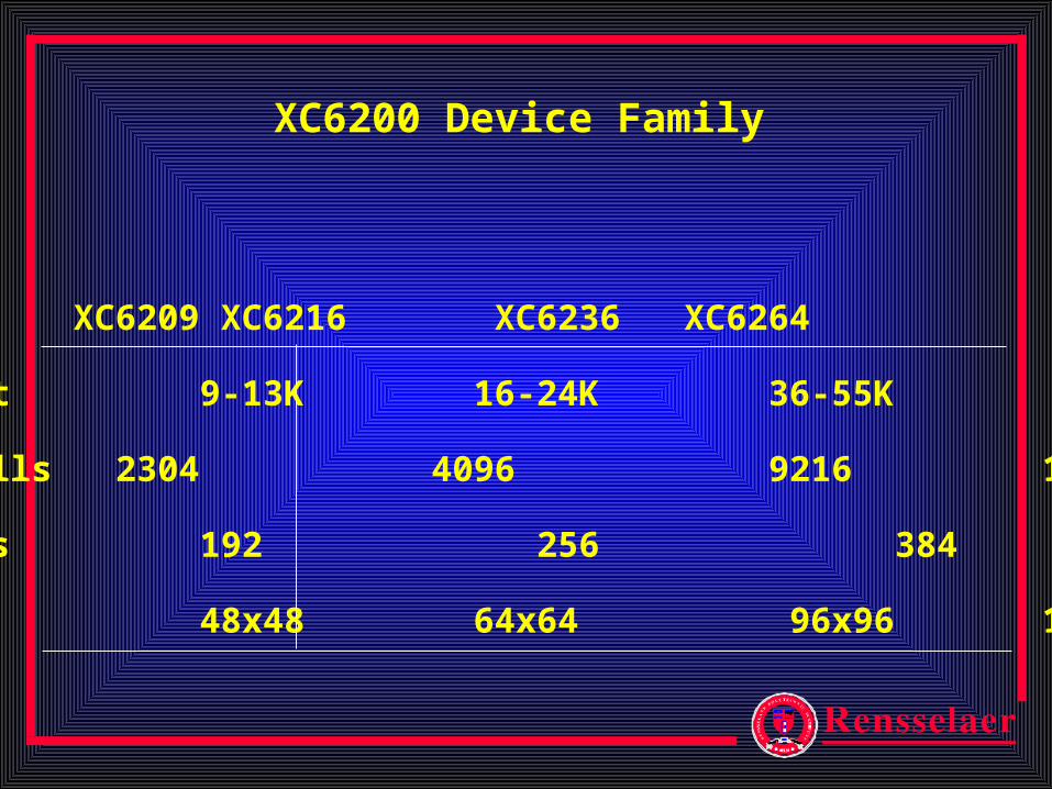
Device XC6209 XC6216 XC6236 XC6264
Gate Count 9-13K 16-24K 36-55K 64-100K
Number Cells 2304 4096 9216 16384
I/O Blocks 192 256 384 512
Row x Col 48x48 64x64 96x96 128x128
XC6200 Device Family
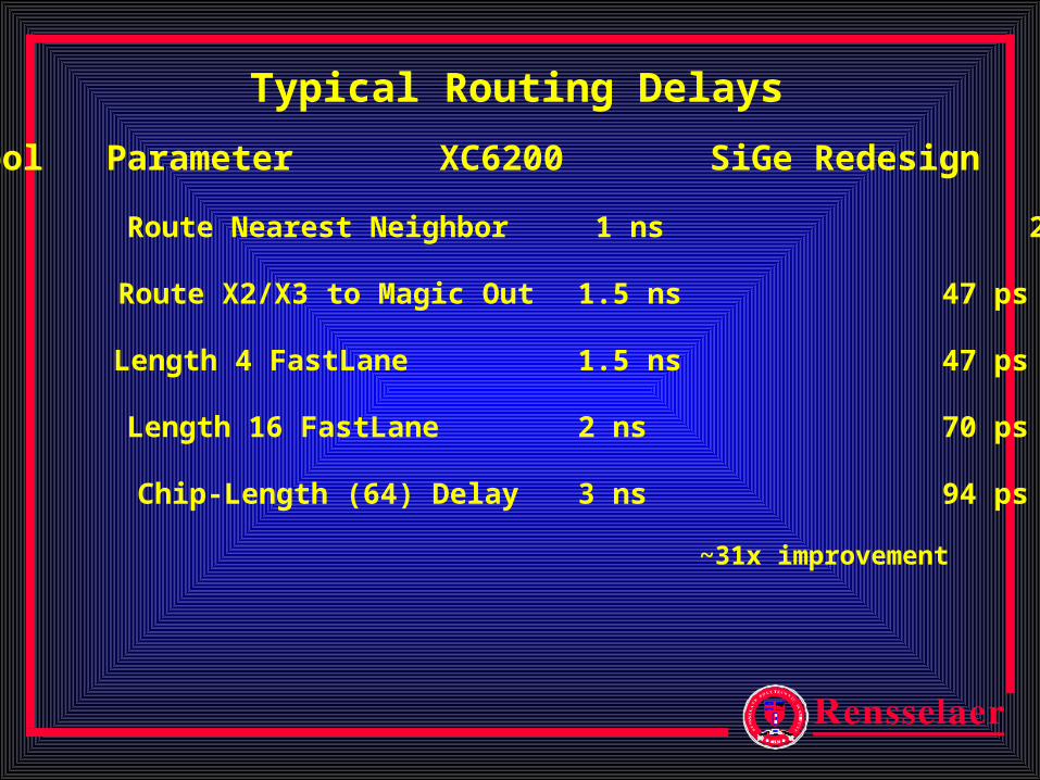
Typical Routing Delays
Symbol Parameter XC6200 SiGe Redesign TNN Route Nearest Neighbor 1 ns 23 ps
Tmagic Route X2/X3 to Magic Out 1.5 ns 47 ps
TL4 Length 4 FastLane 1.5 ns 47 ps
TL16 Length 16 FastLane 2 ns 70 ps
TCL64 Chip-Length (64) Delay 3 ns 94 ps
~31x improvement
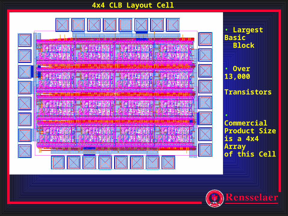
4x4 CLB Layout Cell
• Largest Basic Block
• Over 13,000 Transistors
• CommercialProduct Size is a 4x4 Arrayof this Cell

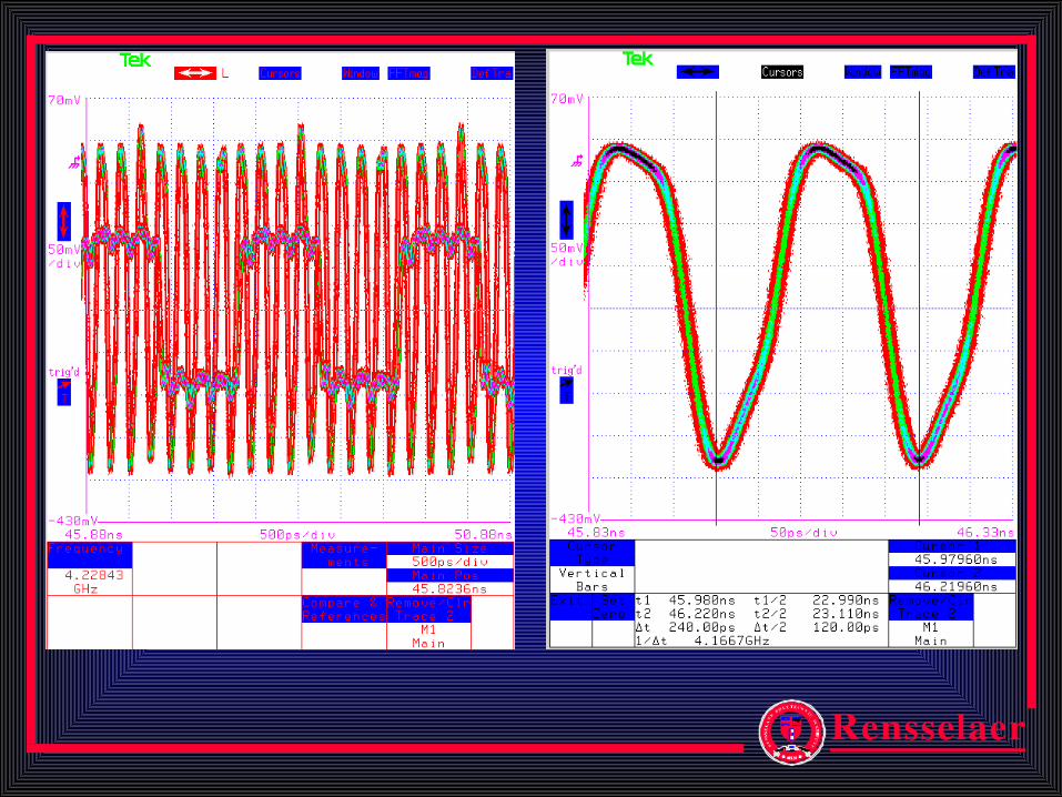
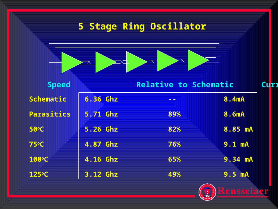
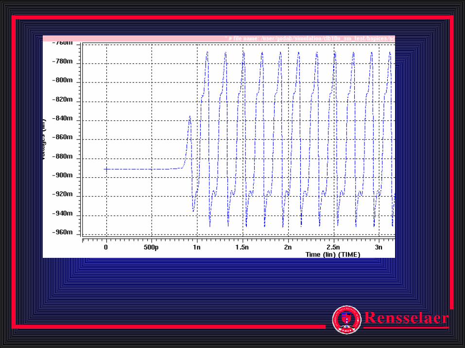
5 Stage Ring Oscillator
Schematic 6.36 Ghz -- 8.4mA
Parasitics 5.71 Ghz 89% 8.6mA
50oC 5.26 Ghz 82% 8.85 mA
75oC 4.87 Ghz 76% 9.1 mA
100oC 4.16 Ghz 65% 9.34 mA
125oC 3.12 Ghz 49% 9.5 mA
Speed Relative to Schematic Current