SiC Auxilliary Power Supply Solutionsfiles.iccmedia.com/events/powercon17/munich_03_rohm.pdf•...
23
© ROHM Semiconductor GmbH 2017 SiC Solution for Industrial Auxilliary Power Supply 05.12.2017 Christian Felgemacher Application Engineer – Power Systems Department
Transcript of SiC Auxilliary Power Supply Solutionsfiles.iccmedia.com/events/powercon17/munich_03_rohm.pdf•...

© ROHM Semiconductor GmbH2017
SiC Solution for Industrial Auxilliary Power Supply
05.12.2017Christian FelgemacherApplication Engineer – Power Systems Department

P. 1© ROHM Semiconductor GmbH.
2017
ROHM’s Power Devices
DeviceSiC (SBD/MOSFET)IGBTHybrid MOSSuper Junction MOSFETFRDSBDShunt Resistor
DiscreteTO220TO247/3PFD-Pak / D2-Paketc…
Power ModuleCase type(Full SiC Module)
Mold typeIPM etc…
ICsGate driverTemperature/High Voltage monitorACDC etc…
ROHM’s power item lineup covers wafers/bare dies, discrete packages, module, ICs and Intelligent Power Modules
Today we focus on an auxilliarysupply solution around discrete
SiC MOSFETs and driving/control IC

P. 2© ROHM Semiconductor GmbH.
2017
*in development
Material Si SiC GaNDevice SJ
MOSFETHybrid MOSFET
FRD IGBT SBD MOSFET HEMT
BreakdownVoltage
500V~800V
600V* 300V600V1200V*
430V650V 1200V*
650V1200V 1700V
650V1200V1700V
R&D*
50+ years experience in Si Transistors/Diodes, 15+ years in WBG Semiconductors.
ROHM‘s power devices

P. 3© ROHM Semiconductor GmbH.
2017
Myths of SiC MOSFET technology
Expensive
Device cost may be higher, but overall system cost equal
or lower

P. 4© ROHM Semiconductor GmbH.
2017
Higher Temp OperationSiSi
SiCSiC
0
50
100
150
200
250
0 5 10 15 20
V GS=18V
16V
14V
12V
10V
8V
6V
4V
2V
0V
Higher Frequency Operation
SiSi SiCSiC
Lower ResistanceSiSi
SiCSiC
Application advantages vs. Si components
Smaller Passive Components
Smaller Size / Higher Efficiency
Simpler Cooling System
Down sizing

P. 5© ROHM Semiconductor GmbH.
2017
Myths of SiC MOSFET technology
Expensive Not reliable
Device cost may be higher, but overall system cost equal
or lower
Extensive reliability testing done,
comparable to Si-based devices

P. 6© ROHM Semiconductor GmbH.
2017
Reliability aspects of SiC Trench MOSFETs
Reliability tests for ROHM Trench MOSFETs
Test IEC Standard Conditions Si SiC Comments SiC
High Temperature Reverse Bias 60747 1000 h @ 95% Vds,max,
Tamb= 125..145°C @ 100% Vds,max
Tamb= Tj,max =175°CHigh Temperature Gate Bias 60747 1000 h @ ±VGS,max,
Tamb= Tj,max
High Humidity High Temperature Reverse Bias
60068-67 1000 h @ Vds,max=80V 85% RH, Tamb= 85°C Vds,max=100V
High Temperature Storage 60068-2-2 1000 h @ TSTG,max
Low Temperature Storage 60068-2-1 1000 h @ TSTG,min
Thermal Cycle 60068-2-14 100 cyclesTSTG,max - TSTG,min
SiC 3 Gen. MOSFETs undergoreliability tests similar to those for Si
MOSFETs and IGBTs Automotive qualification
soon to be finished

P. 7© ROHM Semiconductor GmbH.
2017
Myths of SiC MOSFET technology
Expensive Not reliable Complex
Device cost may be higher, but overall system cost equal
or lower
Extensive reliability testing done,
comparable to Si-based devices
Use of SiC MOSFETs can simplify circuit
design
Todays focus: Simple solution for aux supply

P. 8© ROHM Semiconductor GmbH.
2017
Auxiliary power supplies for industrial applications
System (PV inverter, DC/DC converter, battery charger, etc.)
OUTPUTINPUT
• Auxiliary voltage separated from the main power path
• High voltage input• Low voltage output• Isolated
Main converter
LV subsystems (i.e. control units, sensors, human interfaces, gate drivers)
Auxiliary power supply
24V12V5V

P. 9© ROHM Semiconductor GmbH.
2017
Typical circuit for industrial auxilliary supply
Flyback converter with 3-phase input
Q
AC mains 3ph Vac,in = 210…690V
Vdc,in ≈300…1000V
Reflected voltage from
secondary side
Vrefl ≈100V
Vsurge ≈ 200V(turn-off overshoot)
What is the max. voltage theMOSFET has to withstand?
Vdc,in + Vrefl + Vsurge = 1300V
Device rated voltage: ≥ 1500 V
P. 10© ROHM Semiconductor GmbH.
2017
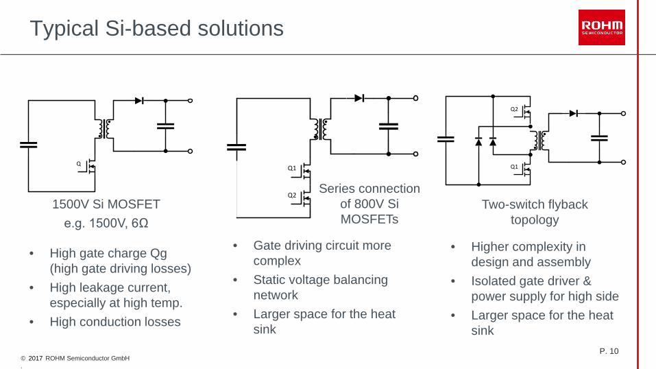
Typical Si-based solutions
• High gate charge Qg(high gate driving losses)
• High leakage current, especially at high temp.
• High conduction losses
Q1
Q2Series connection
of 800V Si MOSFETs
1500V Si MOSFETe.g. 1500V, 6Ω
• Gate driving circuit more complex
• Static voltage balancing network
• Larger space for the heat sink
Two-switch flybacktopology
• Higher complexity in design and assembly
• Isolated gate driver & power supply for high side
• Larger space for the heat sink
Q2
Q1Q

P. 11© ROHM Semiconductor GmbH.
2017
min typ max min typ max min typ max min typ maxV(BR)DSS V 1700 1500 1500 1500Id @ 25°C A 3,7 2 2,5 6Rds(on)@25°C Ω 1,15 1,5 9 12 6 9 2,2 3Idss@25°C µA 0,1 10 500 10 1000Ciss pF 184 990 939 2025Rg Ω 64 4Qg nC 14 29,3 114Rth(j-c) K/W 3,32 4,32 2
NDUL09N150CSCT2H12NZunitProperty 2SK225 STFW3N150
Why use a SiC-MOSFET in this application?
• SiC MOSFET has lower RDS(on)
• Also, Qg and capacitance are much reduced
• High gate resistance of SiC device demands a low-impedance gate drive
Si-MOSFET-A Si-MOSFET-B Si-MOSFET-C

P. 12© ROHM Semiconductor GmbH.
2017
Why use a SiC-MOSFET in this application?
• The underlying advantage is thesignificantly reduced RDS(on)·A valueof SiC MOSFETs vs Si-MOS

P. 13© ROHM Semiconductor GmbH.
2017
Lineup 1700V SiC MOSFET devices:
Part No. VDS[V] RDSon typ[mΩ]@Vgs=18V
ID[A]@TC=25°C
ID[A]@TC=100°C Tjmax[° C] Package Die Part No.
SCT2H12NZ 1700 1150 3,7 2,6 175 TO-3PFM -SCT2H12NY 1700 1150 4,0 2,9 175 TO-268-2L -SCT2750NY 1700 750 5,9 4,0 175 TO-268-2L -
1700 100 34 - 175 bare die S2409
NEWNEW
ROHM SiC-MOSFETs for Auxiliary Power Supplies

P. 14© ROHM Semiconductor GmbH.
2017
TO-268 2L0.75Ω, 1.15Ω
SiC MOSFET in auxiliary power supplies
SiC-based solution with 1700V MOSFET and single-switch flyback topology
• Single switch• Isolated package• Control IC BD768xFJ• Heat sink not mandatory if <40W
Q TO-3PFM1.15Ω
SCT2H12NZ
ROHM evaluation board available
BD7682FJ_EVK_301
80mm
80mm
Input: 300-900 VdcOutput: 12 VdcPower: 40 W (no heat sink)Sw. freq.: 90…120 kHzEfficiency: 85% (300 Vdc), 83% (700 Vdc)
BD768xFJ

P. 15© ROHM Semiconductor GmbH.
2017
SpecificationFeature
Application circuit ApplicationFactory Automation, Adaptor, Smart Meter
Operating VCC Range : 15.0V ~ 27.5VDCDC Max Frequency : 120kHz Operating current 800 uAOperating Temperature: - 40deg. to +105deg.
PIN place / Package
SOP-J8S6.0mm×4.9mm :
1.27mm pitch<TYP>
Optimum System for driving SiC MOSFETQuasi – Resonant DC/DC convertorLow VCC current (19uA@VCC=18.5V)Burst function at light loadMax Frequency Controlled(120kHz)VCC Over Voltage ProtectionVCC Under Voltage Locked OutBrown IN/OUT FunctionDC/DC Soft StartDC/DC Cycle by Cycle current limiter250nsec Leading-Edge BlankingZT Trigger mask function ZT Over Voltage ProtectionOver Load Protection ( 128ms Timer ) MASK Function
Line upFBOLP VCCOVP
BD7682FJ AutoRestart LatchBD7683FJ Latch LatchBD7684FJ AutoRestart AutoRestartBD7685FJ Latch AutoRestart
Control IC
1 2 3 4
5678
VOUT
AC85-265Vac
FUSE+
-
Filter DiodeBridge
OUT
GND
VCC
CSZT
RS
CM
FB
ERRORAMP
PC
BO MASK
VD
VP
VS
巻線比:NP
巻線比:NS
巻線比:ND
NO. Pin
1 ZT Zero Current Detect pin
2 FB Feedback pin
3 CS Current Sense pin
4 GND GND pin
5 OUT MOSFET drive pin
6 MASK External TR drive
7 VCC Power Supply pin
8 BO Broun IN/OUT monitor pin
BD768xFJ-LB’s features

P. 16© ROHM Semiconductor GmbH.
2017
SiC MOSFET in auxiliary power supplies
ROHM evaluation board BD7682FJ_EVK_301
Control IC for SiC based solution: BD768xFJ
• Implements quasi-resonant switching to minimisedynamic losses and achieve low noise
• Suitable drive voltage for SiC MOSFET
Reduced effective switchingvoltage leads to lower turn-on loss

P. 17© ROHM Semiconductor GmbH.
2017
SiC MOSFET in auxiliary power supplies
Waveforms of flyback switch for different operating contitions:
• Quasi-resonant operation is maintained across the output power range• As the delay time decreases the effective switching frequency increases with increased load

P. 18© ROHM Semiconductor GmbH.
2017
Operation at 40W without heat sink (with heat sink ca. 100W possible)
SiC MOSFET in auxiliary power supplies
Sp1
Sp2Sp3
Vout = 12 VDC

P. 19© ROHM Semiconductor GmbH.
2017
FUSE
FilterDiodeBridge
GND
VCC
SOURCE
ZT
FB
ERRORAMP
BO
12
76
54
3
DRAIN
Next step: Integration of SiC MOSFET and controller
Target Specification
ApplicationFactory Automation, Adaptor, Smart Meter
Operating VCC Range : 15.0V ~ 29.5VOperating DRAIN Range ~ 1700VDrain Current ( Continuous ) 4ADrain Current ( Pulsed ) 10ADrain-Source on resistance ca. 1.6 OhmPower Range ( Without Heat-Sink) ca. 30WPower Range ( With Heat-Sink ) ca. 100W
PIN place / PackageNO. Pin
1 DRAIN DRAIN pin
2 SOURCE Current Sense pin
3 FB Feedback pin
4 GND GND pin5 ZT Zero Current Detect pin
6 BO Broun IN/OUT monitor pin
7 VCC Power Supply pin

P. 20© ROHM Semiconductor GmbH.
2017
Next step: Integration of SiC MOSFET and controller
Block diagramAdditional features (tbc)
NOUT+
-
+
VOUTFUSE
FilterDiodeBridge
Leading EdgeBlanking
DRAIN
GND
VCC
SOURCE
+
-
InternalSupply
ZTZT
Comp.
RS
Czt
FB
VREF(4V)
2
5
7
4
3
18.5V/14.0V
28.0V
Timer(128ms)
FBOLP_OH
+
-
100mV/400mV
1 shot
OSC
Cfb
ERRORAMP
PC
OSCRzt1
7V
AND
ZT BlankingOUT(H->L)
0.60us NOUT
TimeOut( 15 usec )
AND
ANDPRE
Driver
POUT
FB/2
+
--
DCDC Comp.
1.00V
+
-
VCC OVP
CURRENT SENSE (V-V Change)Normal : ×1.0
+
-
FBOLP_OH
MAX Blanking
Frequency(120kHz)
1.00V
0.50V
+
-
OLP
200kΩ
200kΩ
VCC UVLO
BurstComp.
6BO
4.0V Regulator
Soft Start
+
-
1.0V
RH
RL
BOComp.
OR
OR
15uA
20k
+
-ZT ACSNS Comp.
SS1ms SS4ms
Va
Rstart
Cvcc
VH
Rzt2
+
- ZT OVP Comp. (LATCH)
S Q
R
NOUT
18.0V Clamper
1
• VCC Over Voltage Protection• VCC Under Voltage Lock Out• Soft Start• Cycle by Cycle current limiting• Burst function• Over-load protection• Brown-out• Gate voltage clamping
• etc.

P. 21© ROHM Semiconductor GmbH.
2017
Conclusions
• Auxilliary supply solution using BD768xFJ with 1700V SiCMOSFET is a good alternative to auxilliary supply circuits thattoday use series connection of Si MOSFETs or complex topologies to achieve the desired blocking voltage level.
• Taking advantage of SiC device benefits cost advantages canbe realised on the system level.
• The next development step for SiC based auxilliary supplysolutions is integration of the control IC and power switch in one package.

© 2017 ROHM Semiconductor GmbH


![Chapter 2 SiC Materials and Processing Technology€¦ · 34 2 SiC Materials and Processing Technology Table 2.1 Key electrical parameters of SiC [1] Property 4H-SiC 6H-SiC 3C-SiC](https://static.fdocuments.us/doc/165x107/5f4fd11797ddad63bf719816/chapter-2-sic-materials-and-processing-technology-34-2-sic-materials-and-processing.jpg)