Si4010 Antenna Interface and Matching Network Guide -- AN369
36
Rev. 0.2 4/11 Copyright © 2011 by Silicon Laboratories AN369 This information applies to a product under development. Its characteristics and specifications are subject to change without notice. Silicon Laboratories Confidential. Information contained herein is covered under non-disclosure agreement (NDA). AN369 Si4010 A NTENNA I NTERFACE AND M ATCHING N ETWORK G UIDE 1. Introduction This document provides guidelines and design examples for the high impedance matching networks and loop antennas necessary for the proper usage of the Si4010 transmitter. Section “2. High Impedance Differential Power Amplifier” gives a brief overview of the differential high impedance PA used in this chip. It also describes the method for determining the optimum termination impedance necessary to acquire the maximum power with the best efficiency. Section “3. Inductively Tapped Loop Antenna Design Example”describes basic design steps, simulation, and measurement results for an inductively tapped printed loop antenna working at 434 MHz with the Si4010 chip and with the SOIC package. It also gives measurement data and dimensions for a 868 MHz loop antenna version. Section “3.1. 434 MHz Antenna Dimensions and Measured Data”shows the realized loop antenna with dimensions and the test results. This section is devoted to readers who are not greatly interested in the design details of the antenna; rather, they are concerned with quickly obtaining dimension, layout, and measurement data. Section “3.2. 868 MHz Antenna Dimensions and Measured Data with Si4010-C2-GS”briefly summarizes the measured results and dimensions of the 868 MHz tapped loop antenna. Section “4. Matching Balun Design for Si4010 with 50 Single-Ended Output” describes the design steps for the matching balun, which matches the high impedance differential outputs of the Si4010 chip to a 50 single-ended termination or antenna such as monopole, spiral, ILA, etc. Section “4.1. Matching Baluns for Si4010_B1 with SOIC and MSOP Package”gives the matching network schematic and measured results for both the SOIC and MSOP packages. These sections are useful for readers who are not greatly interested in the theoretical development of the matching network but who are concerned with quickly obtaining a set of component values for a given desired frequency of operation. Section “5. Design of High Q Discrete Matching Baluns” describes the design procedure and operation of the matching. 2. High Impedance Differential Power Amplifier This section discusses the operation of the high impedance class A power amplifier used in the Si4010 chips. In theory the delivered power to the load is maximum if the RF generator is terminated by the complex conjugate of its generator impedance. This is called optimum conjugate matching. However, it is true only if no constraints for voltage swing are given. Operation of the high impedance PA is illustrated in Figure 1. High impedance PAs usually have open drain outputs and behave like a RF current generator. The TX generator impedance is represented by its parallel RC equivalent while the termination by its parallel RL equivalent. The L AP and C TX work in high impedance parallel resonance at the operation frequency and thus the voltage swing is determined by the residual equivalent resistance of the termination (R AP ) and the TX internal loss (EPR). The drain voltage is limited by the CMOS technology. With a fixed current magnitude I RF , if the generator impedance is too high, the voltage swing would exceed the limit with complex conjugate termination.
Transcript of Si4010 Antenna Interface and Matching Network Guide -- AN369

Rev. 0.2 4/11 Copyright © 2011 by Silicon Laboratories AN369This information applies to a product under development. Its characteristics and specifications are subject to change without notice.
Silicon Laboratories Confidential. Information contained herein is covered under non-disclosure agreement (NDA).
AN369
Si4010 ANTENNA INTERFACE AND MATCHING NETWORK GUIDE
1. Introduction
This document provides guidelines and design examples for the high impedance matching networks and loopantennas necessary for the proper usage of the Si4010 transmitter.
Section “2. High Impedance Differential Power Amplifier” gives a brief overview of the differential high impedancePA used in this chip. It also describes the method for determining the optimum termination impedance necessary toacquire the maximum power with the best efficiency.
Section “3. Inductively Tapped Loop Antenna Design Example”describes basic design steps, simulation, andmeasurement results for an inductively tapped printed loop antenna working at 434 MHz with the Si4010 chip andwith the SOIC package. It also gives measurement data and dimensions for a 868 MHz loop antenna version.
Section “3.1. 434 MHz Antenna Dimensions and Measured Data”shows the realized loop antenna with dimensionsand the test results. This section is devoted to readers who are not greatly interested in the design details of theantenna; rather, they are concerned with quickly obtaining dimension, layout, and measurement data.
Section “3.2. 868 MHz Antenna Dimensions and Measured Data with Si4010-C2-GS”briefly summarizes themeasured results and dimensions of the 868 MHz tapped loop antenna.
Section “4. Matching Balun Design for Si4010 with 50 Single-Ended Output” describes the design steps for thematching balun, which matches the high impedance differential outputs of the Si4010 chip to a 50 single-endedtermination or antenna such as monopole, spiral, ILA, etc.
Section “4.1. Matching Baluns for Si4010_B1 with SOIC and MSOP Package”gives the matching networkschematic and measured results for both the SOIC and MSOP packages. These sections are useful for readerswho are not greatly interested in the theoretical development of the matching network but who are concerned withquickly obtaining a set of component values for a given desired frequency of operation.
Section “5. Design of High Q Discrete Matching Baluns” describes the design procedure and operation of thematching.
2. High Impedance Differential Power Amplifier
This section discusses the operation of the high impedance class A power amplifier used in the Si4010 chips. Intheory the delivered power to the load is maximum if the RF generator is terminated by the complex conjugate of itsgenerator impedance. This is called optimum conjugate matching. However, it is true only if no constraints forvoltage swing are given.
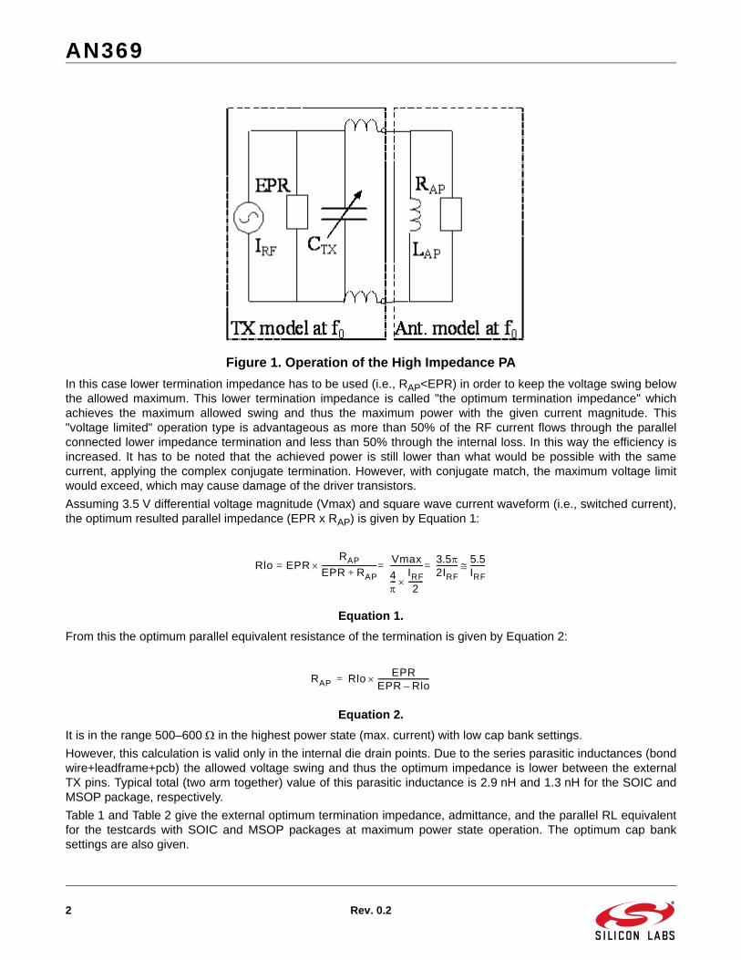
Operation of the high impedance PA is illustrated in Figure 1. High impedance PAs usually have open drain outputsand behave like a RF current generator. The TX generator impedance is represented by its parallel RC equivalentwhile the termination by its parallel RL equivalent. The LAP and CTX work in high impedance parallel resonance atthe operation frequency and thus the voltage swing is determined by the residual equivalent resistance of thetermination (RAP) and the TX internal loss (EPR).
The drain voltage is limited by the CMOS technology. With a fixed current magnitude IRF, if the generatorimpedance is too high, the voltage swing would exceed the limit with complex conjugate termination.
AN369
2 Rev. 0.2
Figure 1. Operation of the High Impedance PA
In this case lower termination impedance has to be used (i.e., RAP<EPR) in order to keep the voltage swing belowthe allowed maximum. This lower termination impedance is called "the optimum termination impedance" whichachieves the maximum allowed swing and thus the maximum power with the given current magnitude. This"voltage limited" operation type is advantageous as more than 50% of the RF current flows through the parallelconnected lower impedance termination and less than 50% through the internal loss. In this way the efficiency isincreased. It has to be noted that the achieved power is still lower than what would be possible with the samecurrent, applying the complex conjugate termination. However, with conjugate match, the maximum voltage limitwould exceed, which may cause damage of the driver transistors.
Assuming 3.5 V differential voltage magnitude (Vmax) and square wave current waveform (i.e., switched current),the optimum resulted parallel impedance (EPR x RAP) is given by Equation 1:
Equation 1.
From this the optimum parallel equivalent resistance of the termination is given by Equation 2:
Equation 2.
It is in the range 500–600 in the highest power state (max. current) with low cap bank settings.
However, this calculation is valid only in the internal die drain points. Due to the series parasitic inductances (bondwire+leadframe+pcb) the allowed voltage swing and thus the optimum impedance is lower between the externalTX pins. Typical total (two arm together) value of this parasitic inductance is 2.9 nH and 1.3 nH for the SOIC andMSOP package, respectively.
Table 1 and Table 2 give the external optimum termination impedance, admittance, and the parallel RL equivalentfor the testcards with SOIC and MSOP packages at maximum power state operation. The optimum cap banksettings are also given.
Rlo EPRRAP
EPR RAP+------------------------------=
Vmax
4---
IRF
2--------
------------------ 3.52IRF------------ 5.5
IRF--------==
RAP RloEPR
EPR Rlo–----------------------------=

AN369
Rev. 0.2 3
The voltage limited operation mode is typical at the highest power settings (highest current) of the Si4010 chip,where the delivered power to the optimum differential termination is ~ +10 dBm.
A second important operation mode is when the current magnitude is reduced (e.g. to reduce the power) and thusthe maximum allowed voltage swing is not achieved even if the conjugate complex termination is applied. In thiscase the PA is "current limited". This is the typical case when the Si4010 chip works in a strongly reduced powerstate or when the internal capacitance bank state is high (close to maximum at low bands and above ~100 in highbands). In this operation mode the optimum termination is the complex conjugate.
A third, non-optimum mode is when the current is maximum, but the termination impedance is so low that themaximum swing is not achieved. In this case the termination is not the optimum, and the power and efficiency islower than the possible maximum. All operation modes are covered and the parameters can be calculated easilyby the 401x calculator: e.g., the parallel equivalent of the optimum termination can be found in the “Antenna Target”fields. More details about this calculator can be found in AN457.
Table 1. SOIC Maximum Power Operation
Freq [MHz]
SOICOpt. load imp. []
Opt. load adm.
[mSie]
Parallel Eqv. RAP
[]
Parallel Eqv. LAP
[nH]
Cap. bank state & TX equivalent
capacitance (CTX)
Power to the differential load [dBm]
315 28.6+j114 2.07-j8.25 483 61.2 99, 4.17 pF 10.7
434 32.5+j120 2.09-j7.74 479 47.4 23, 2.84 pF 10.6
868 8.1+j58 2.39-j17 419 10.8 17; 3.12 pF 9.7
915 7.1+j54 2.45-j18.3 409 9.7 17, 3.19 pF 9.6
Table 2. MSOP Maximum Power Operation
Freq [MHz]
MSOPOpt. load imp. []
Opt. load adm.
[mSie]
Parallel Eqv. RAP
[]
Parallel Eqv. LAP
[nH]
Cap. bank state & TX equivalent
capacitance
Power to the differential load [dBm]
315 27+j114 1.98-j8.3 505 60.8 105, 4.2 pF 10.7
434 32.3+j124 19.7-j7.6 508 48.5 23, 2.77 pF 10.6
868 8.3+j66 1.88-j14.9 532 12.3 13, 2.73 pF 9.8
915 7.3+j62 1.87-j15.9 535 11 13, 2.76 pF 9.7

AN369
4 Rev. 0.2
3. Inductively Tapped Loop Antenna Design Example
3.1. 434 MHz Antenna Dimensions and Measured DataThis antenna design uses the Si4010-C2-GS version of the Si4010 chip. The designed antenna top layout withfinal outer dimensions is shown in Figure 2. The bottom layout is shown in Figure 3. The schematic is shown inFigure 4. The manufacturing pack (including CAM/CAD/PDF files and the BOM) is available at www.silabs.com.The whole unit is encapsulated by the Polycase FB-20 plastic enclosure as shown in Figure 5 and Figure 6.
Figure 2. Antenna Top Layout with Final Outer Dimensions

AN369
Rev. 0.2 5
Figure 3. Antenna Bottom Layout with Final Outer Dimensions
AN369
6 Rev. 0.2
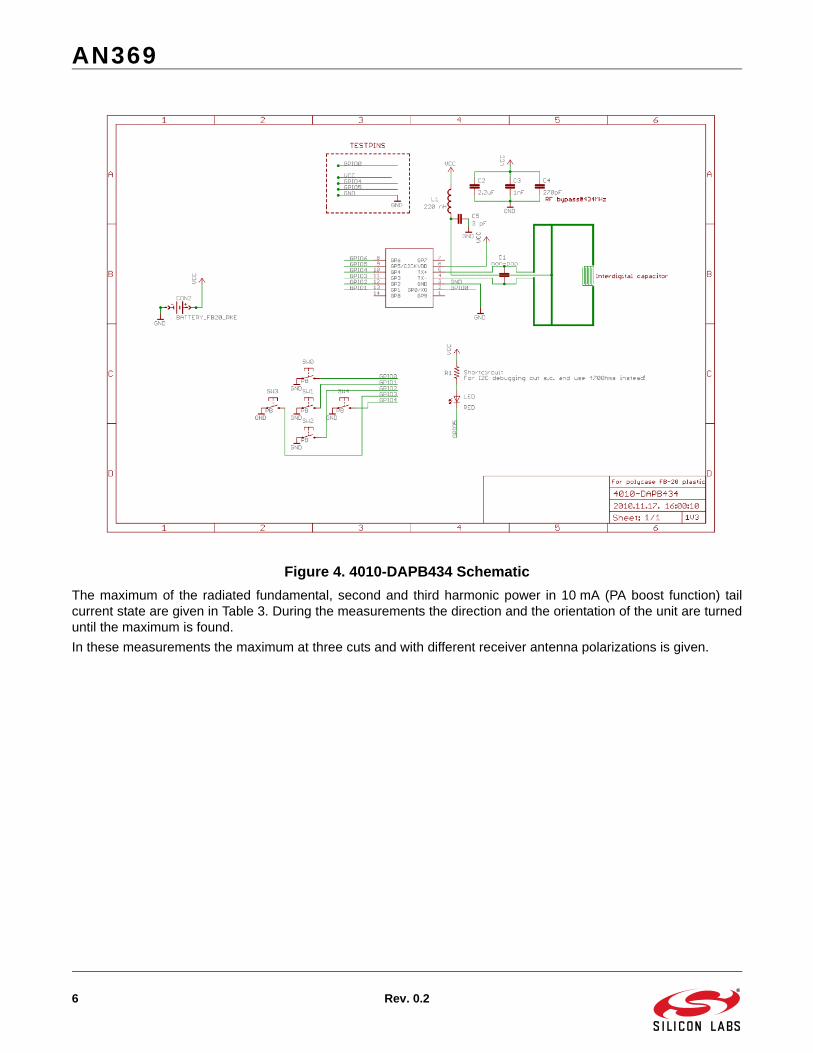
Figure 4. 4010-DAPB434 Schematic
The maximum of the radiated fundamental, second and third harmonic power in 10 mA (PA boost function) tailcurrent state are given in Table 3. During the measurements the direction and the orientation of the unit are turneduntil the maximum is found.
In these measurements the maximum at three cuts and with different receiver antenna polarizations is given.

AN369
Rev. 0.2 7
Table 3. Maximum of the Radiated Fundamental, Second and Third Harmonic Power of the 4010-DAPB434 Board
EIRP [dBm]
H-pol receiver, 10 mA
Plane
XY ZY ZX
434 MHz –11.39 –19.37 –19.83
868 MHz –54.3 –55.4 –58.6
1302 MHz –43.65 –48.5 –57.15
V-pol receiver, 10mA
Plane
XY ZY ZX
434 MHz –30.61 –17.67 –18.42
868 MHz –58.6 –52.3 –50.8
1302 MHz –51.75 –42.75 –37
AN369
8 Rev. 0.2
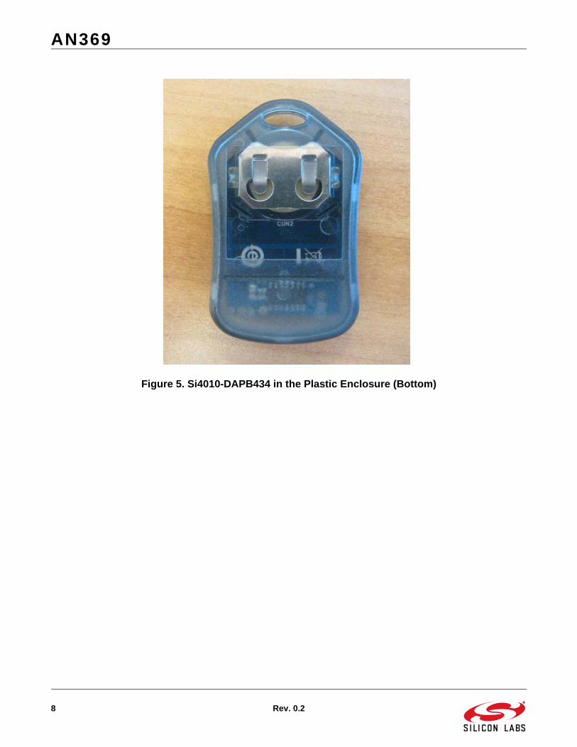
Figure 5. Si4010-DAPB434 in the Plastic Enclosure (Bottom)

AN369
Rev. 0.2 9
Figure 6. Si4010-DAPB434 in the Plastic Enclosure (Top)
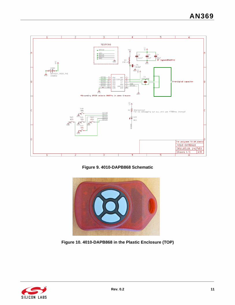
3.2. 868 MHz Antenna Dimensions and Measured Data with Si4010-C2-GSThis antenna design uses the Si4010-C2-GS version of the Si4010 chip. The designed antenna top layout withfinal outer dimensions is shown in Figure 7. The bottom layout is shown in Figure 8. The schematic is shown inFigure 9. The manufacturing pack (including CAD/CAM/PDF files and the BOM) is available at www.silabs.com.The whole unit is encapsulated by the Polycase FB-20 plastic enclosure as shown in Figure 10 and Figure 11.

AN369
10 Rev. 0.2
Figure 7. Antenna Layout with Final Outer Dimensions
Figure 8. Antenna Bottom Layout
AN369
Rev. 0.2 11
Figure 9. 4010-DAPB868 Schematic
Figure 10. 4010-DAPB868 in the Plastic Enclosure (TOP)
AN369
12 Rev. 0.2
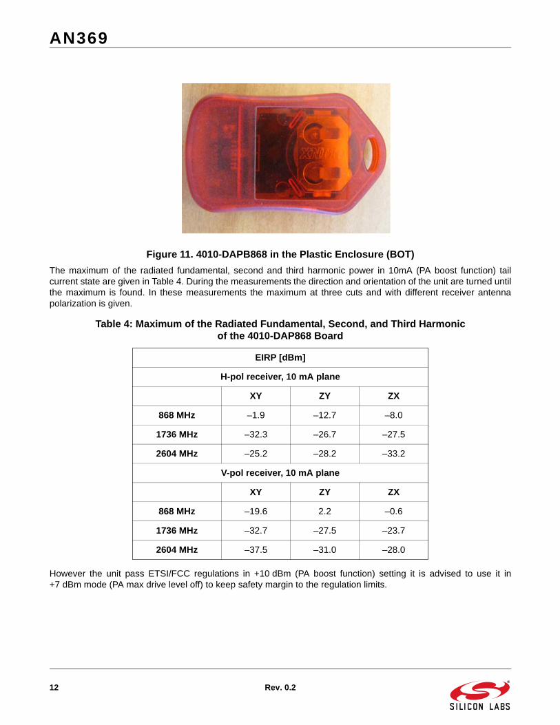
Figure 11. 4010-DAPB868 in the Plastic Enclosure (BOT)
The maximum of the radiated fundamental, second and third harmonic power in 10mA (PA boost function) tailcurrent state are given in Table 4. During the measurements the direction and orientation of the unit are turned untilthe maximum is found. In these measurements the maximum at three cuts and with different receiver antennapolarization is given.
However the unit pass ETSI/FCC regulations in +10 dBm (PA boost function) setting it is advised to use it in+7 dBm mode (PA max drive level off) to keep safety margin to the regulation limits.
Table 4: Maximum of the Radiated Fundamental, Second, and Third Harmonicof the 4010-DAP868 Board
EIRP [dBm]
H-pol receiver, 10 mA plane
XY ZY ZX
868 MHz –1.9 –12.7 –8.0
1736 MHz –32.3 –26.7 –27.5
2604 MHz –25.2 –28.2 –33.2
V-pol receiver, 10 mA plane
XY ZY ZX
868 MHz –19.6 2.2 –0.6
1736 MHz –32.7 –27.5 –23.7
2604 MHz –37.5 –31.0 –28.0

AN369
Rev. 0.2 13
3.3. Detailed Antenna Design Steps Using a Planar EM Simulator (Sonnet)For the antenna design the Sonnet 2.5D EM simulator is used. The goal is to design the optimum antennaimpedance for the PA which results in the maximum power delivery to the antenna at cap bank state 80. Thereactance of this optimum antenna impedance is resonating with the PA output capacitance at internal capacitancebank state of 80. That is close to the lower edge of the output capacitance tuning range of the Si4010 (0–511) inorder to increase the Q factor of the PA and thus decrease the internal losses. A basic EM simulated planarstructure is shown in Figures 12–14.
Figure 12. Antenna Simulation (Bottom)

AN369
14 Rev. 0.2
Figure 13. Antenna Simulation (Top)
Figure 14. Antenna Simulation in 3D

AN369
Rev. 0.2 15
The antenna is fed from the left side through a differential transmission line. This transmission line is de-embeddedfrom the simulation by port extension. The reference plane of the simulation is shown by the black arrows. Theground planes on both side of the transmission line represent the PCB area of the unit’s circuitry. The antenna is aninductively tapped loop with the series capacitance in the main loop realized by a printed interdigital capacitor.
The usage of an interdigital printed capacitor has many advantages:
Fine-tuning possible
No need for an extra component
Reduced value spreading due to the interdigital technique
In this design concept the Si4010 and the whole circuitry is outside of the antenna area. With this structure, outsideconnection to the circuitry is easier. In theory, the whole circuit could be placed inside the antenna area.Unfortunately, the increase of the useful antenna area due to this would be negligible but the interfacing of thecircuitry would be much more difficult.
The unit is working from a CR2032 battery. The battery is placed at the bottom side beneath the printed capacitor(see the round shape battery’s pad at the bottom layer in Figure 3.) In this way:
The interdigital capacitor does not occupy additional space from the antenna area.
The battery and the metallization around it give some shielding and thus reduce the detuning of the printed capacitor in the vicinity of a hand.
The simulation box size is: 180 mm due to 128 MB memory restrictions of the applied Sonnet level version. Withthis box size, the boundaries are far enough to avoid the disturbance of the antenna near field and thus the reactiveimpedance part (i.e., the antenna inductance) estimation is quite accurate. Unfortunately, the distance is not bigenough to accurately estimate the far field radiation of the antenna. Due to this, the antenna gain and the radiationresistance is not accurately simulated. With a bigger boundary box, which consumes more memory and requires ahigher level Sonnet V11 EM license, accurate far field simulation is possible. Also the structure can have amaximum of 2 metal layers and 6 ports with this Sonnet level. Despite this, the real part of the antenna impedanceis estimated relatively well as the ohmic and dielectric loss is usually dominant compared to the radiated loss incase of small loop antennas. During the simulation, the antenna is terminated by an ideal capacitance whichmodels the Si4010 output capacitance at cap bank state 80. Its typical value is ~3.8 pF. The antenna and the PAcapacitance together form a parallel resonant circuit and with proper antenna design the resonance occurs at thetargeted operation frequency.
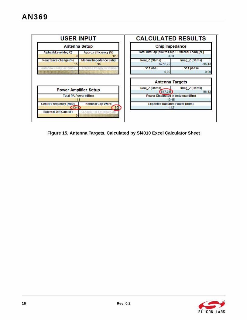
Figure 15 shows the used impedance parameters derived by the Si4010 optimum antenna impedance calculator(Si4010_calc_regs_100928.xls). According to this, the optimum values in the parallel RL equivalent of the antennaare: Real_Z=517 , ImagZ=96.43 at 434 MHz. It corresponds to 35.4 nH antenna inductance which is inresonance with the 4010 output capacitance (3.8 pF) at 434 MHz.
AN369
16 Rev. 0.2
Figure 15. Antenna Targets, Calculated by Si4010 Excel Calculator Sheet

AN369
Rev. 0.2 17
Simulated impedance:
The simulated antenna impedance with 3.8 pF at the input is shown in Figure 16. The resonance is near 434 MHz(the slight detuning will be compensated by the automatic tuning).
The residual impedance at resonance is ~517 .
Note: Accurate tuning of the real impedance part is difficult due to the strong tapping ratio.
Figure 16. S11 Real/Img Resonance at 434 MHz, Cload=3.8 pF

AN369
18 Rev. 0.2
4. Matching Balun Design for Si4010 with 50 Single-Ended Output
The Si4010 transmitter can be used with single-ended 50 antennas (monopole, spiral, ILA, IFA, etc.) as well if anexternal matching balun is used between the high impedance differential output of the chip and the 50 single-ended load. The matching balun performs four important tasks with minimal insertion loss:
Provides the optimum termination impedance (see Section “2. High Impedance Differential Power Amplifier”) to the differential output of the chip if the single-ended port of the balun is terminated by 50 . At high power states the differential output is usually not terminated in the complex conjugate way. (See the "voltage limited" operation mode in Section “2. High Impedance Differential Power Amplifier”. In this case, the S11 parameter will not provide good return loss at the 50 port, but the matching will provide the possible highest power.)
Makes the balun function, i.e. adds the two differential outputs in-phase, with equal magnitudes.
Makes suppression on the 2nd harmonic by using a 2nd harmonic trap.
Unfortunately, as the Si4010 outputs are working with the termination (here, the differential port of the balun) withhigh Q parallel resonance, optimum wideband solution is very difficult or even impossible to design.
If the power requirement is significantly relaxed, a possible wideband solution can be to use a coil-type balun. Inthis case, however, the termination impedance is far from optimum and the power is lower (i.e, this is acompromise).
In this application note narrowband, nearly optimum matching baluns are described, which use 0402SMDelements with different element values at the different bands.
In the design the losses and parasitic of the SMD elements and the pcb traces are compensated, and due to this itis strongly recommended to use the pcb layout proposed by Silicon Labs.
Also to comply with regulatory standards (ETSI, FCC, etc.), additional 3rd order filtering is necessary at the single-ended side. The proposed balun circuits comprise these filter sections.
AN369
Rev. 0.2 19
4.1. Matching Baluns for Si4010_B1 with SOIC and MSOP PackageThis section is useful for readers who do not intend to deeply understand the fundamental operation of the high Qmatching balun, but rather are concerned with quickly obtaining a set of component values for a given desiredfrequency of operation.
The presented baluns shows nearly the optimum impedances listed in Table 1 and Table 2 on page 3 for theSi4010 outputs if the single-ended port is terminated by 50 .
Also in the balun function the magnitude mismatch is lower than 6% (typically 2-3%) and the phase error is lowerthan 5 degrees (typically 2 degrees). Fortunately, these levels of residual losses have minimal effect (~0.1 dB) onthe operation of the matching balun. The main sources of these mismatches are the discrete steps of the availableSMD components.
In the design, the losses and parasitic of the SMD elements and the pcb traces are compensated. Due to this it isstrongly recommended to use the pcb layout designs proposed by Silicon Labs around the Si4010 outputs, VDD,grounding, etc.
The loss of the matching core is ~0.5 dB typically. The filters introduce 0.3–0.5 dB additional loss at the operationfrequency. These loss values are achieved by using high Q wirewound inductor (Coicraft 0402HP series) andcapacitor (Murata GRM155 series) types. Usage of lower Q elements (e.g., multilayer inductors) can cause 0.5–1 dB additional loss.
The presented baluns comply with regulatory standards, and for this they comprise the filters at their 50 side.
4.1.1. SOIC Matching Baluns
The schematic of the balun proposed for the SOIC packaged Si4010 is shown in Figure 17. The element values argiven in Table 5.

AN369
20 Rev. 0.2
Figure 17. Si4010 SOIC Matching Network Schematic
The top layer of the Silicon Labs testcard is shown in Figure 17. It is recommended to copy and use the RF layoutaround the chip as it is. The gerbers of the board can be found on the Silicon Labs website.
Unfortunately, around 2.2 GHz, the 50 balun core output (at the C1 capacitor, before the filter) has a very lowimpedance and thus the filter could not attenuate properly. To avoid this, a 8.5 mm long 50 coplanar transmission line is introduced between the C1 capacitor and the filter. This line transforms theimpedance to higher values around 2.2 GHz. In this way, significant reduction of the harmonics around thisfrequency (5th of the 434 MHz and 3rd of the 868 MHz board) is achieved.
Table 5. Matching Element Values for SOIC Packaged Si4010
SOIC LS1 C3 LS2 LS4 CS1 CS2 LS3 LS5 CS5 CS6 CS4
315M 220 nH 4.7 pF 20 nH 20 nH 5.6 pF 3 pF 100 nH 25 nH 8.2 pF 8.2 pF 390 pF
434M 220 nH 2.7 pF 16 nH 16 nH 3.9 pF 2 pF 56 nH 18 nH 6.8 pF 6.8 pF 270 pF
868M 120 nH 3 pF 2.7 nH 2.7 nH 2.7 pF 1.5 pF 24 nH 6.8 nH 5.1 pF 5.1 pF 68 pF
915M 120 nH 3.3 pF 2 nH 2 nH 2.7 pF 1.5 pF 24 nH 6.8 nH 3.9 pF 3.9 pF 56 pF

AN369
Rev. 0.2 21
Figure 18. Top Layout of the SI Testcard with SOIC Packaged Si4010
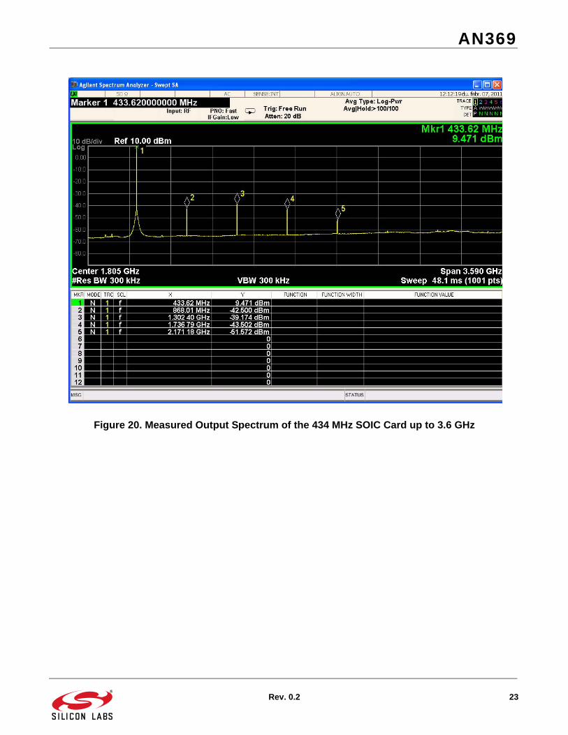
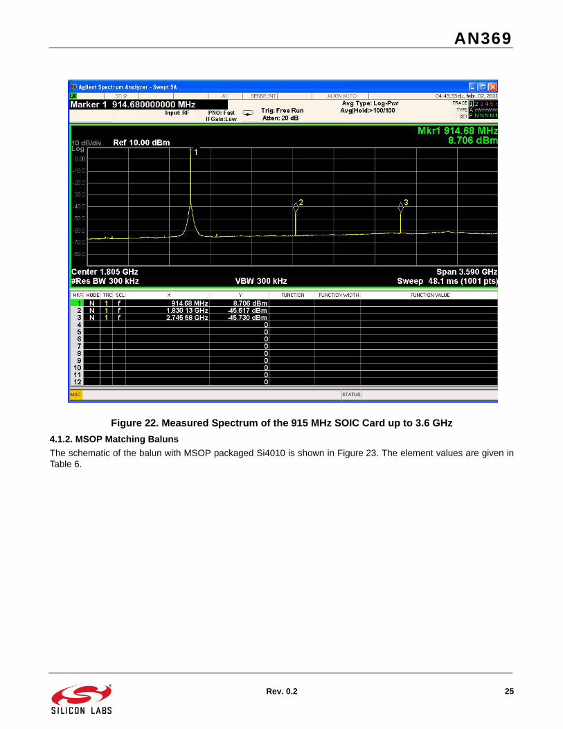
The measured conducted spectrum of the 315, 434, 868, and 915 MHz testcard up to 3.6 GHz is shown in Figures19, 20, 21, and 22, respectively. The realized matchings have ETSI compliance at 434 and 868 MHz and FCCcompliance at 315, 434, and 915 with properly reduced power in this conductive measurement. Assuming 0 dBgain antenna, the compliance will be observed in radiated measurements as well.
The typical power with SOIC package is ~9.5 dBM at low bands and ~8.5 dBM at high bands. Due to the loss of thematch and the filter, the power delivered by the 4010 output is at least 1 dB higher. That is the power delivered to aproperly designed differential antenna input having the optimum impedance without external tuning elements.

AN369
22 Rev. 0.2
Figure 19. Measured Output Spectrum of the 315MHz SOIC Card Up to 3.6 GHz
AN369
Rev. 0.2 23
Figure 20. Measured Output Spectrum of the 434 MHz SOIC Card up to 3.6 GHz

AN369
24 Rev. 0.2
Figure 21. Measured Output Spectrum of the 868 MHz SOIC Card up to 3.6 GHz
AN369
Rev. 0.2 25
Figure 22. Measured Spectrum of the 915 MHz SOIC Card up to 3.6 GHz
4.1.2. MSOP Matching Baluns
The schematic of the balun with MSOP packaged Si4010 is shown in Figure 23. The element values are given inTable 6.

AN369
26 Rev. 0.2
Figure 23. Si4010 MSOP Matching Network Schematic
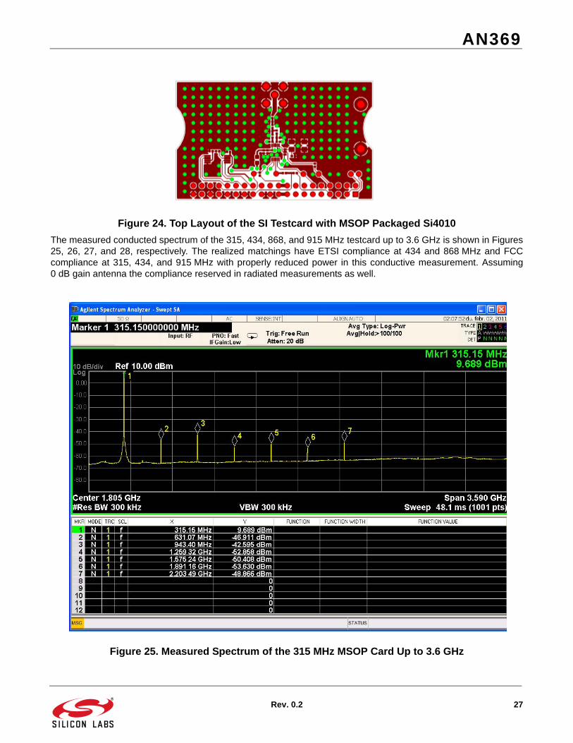
The top layer of the Silicon Labs testcard is shown in Figure 24. It is recommended to copy and use the RF layoutaround the chip as it is. The gerbers of the board can be found on the Silicon Labs website.
Table 6. Matching Element Values for MSOP Packaged Si4010
MSOP LM1 CM3 LM2 LM4 CM1 CM2 LM3 LM5 CM5 CM6 CM4
315M 220 nH 4.7 pF 20 nH 20 nH 5.6 pF 3 pF 120 nH 25 nH 8.2 pF 8.2 pF 390 pF
434M 220 nH 2.7 pF 16 nH 16 nH 4.3 pF 1.8 pF 56 nH 18 nH 6.8 pF 6.8pF 270 pF
868M 120 nH 2.4 pF 3.6 nH 3.6 nH 2.4 pF 1.2 pF 30 nH 6.8 nH 5.1 pF 5.1 pF 68 pF
915M 120 nH 2.4 pF 3.3 nH 2.7 nH 2 pF 1 pF 24 nH 6.2 nH 5.1 pF 5.1 pF 56 pF
AN369
Rev. 0.2 27
Figure 24. Top Layout of the SI Testcard with MSOP Packaged Si4010
The measured conducted spectrum of the 315, 434, 868, and 915 MHz testcard up to 3.6 GHz is shown in Figures25, 26, 27, and 28, respectively. The realized matchings have ETSI compliance at 434 and 868 MHz and FCCcompliance at 315, 434, and 915 MHz with properly reduced power in this conductive measurement. Assuming0 dB gain antenna the compliance reserved in radiated measurements as well.
Figure 25. Measured Spectrum of the 315 MHz MSOP Card Up to 3.6 GHz

AN369
28 Rev. 0.2
Figure 26. Measured Output Spectrum of the 434 MHz MSOP Card Up to 3.6 GHz

AN369
Rev. 0.2 29
Figure 27. Measured Output Spectrum of the 868 MHz MSOP Card Up to 3.6 GHz

AN369
30 Rev. 0.2
Figure 28. Measured Output Spectrum of the 915 MHz MSOP Card Up to 3.6 GHz

AN369
Rev. 0.2 31
5. Design of High Q Discrete Matching Baluns
This section is useful for readers who intend to understand the fundamental operation of the high Q discretematching baluns.
The designed baluns shows nearly the optimum impedances listed in Table 1 and Table 2 on page 3 for the Si4010outputs if the single-ended port is terminated by 50 .
As mentioned previously, the two main tasks the matching balun performs with minimal insertion loss are:
Shows the optimum termination impedance (see Section “2. High Impedance Differential Power Amplifier”) to the differential output of the chip if the single-ended port of the balun is terminated by 50 .
Makes the balun function, i.e., adds the two differential outputs in-phase, with equal magnitudes.
Also it has an additional function to trap and remove the 2nd harmonic.
These functions can be satisfied with optimum solution in narrowband only. This section shows the design hints ofnarrowband discrete baluns.
5.1. Design ProcedureThe basic structure which theoretically satisfies the two main matching balun function has four external elementsas shown in Figure 29. C_TX in the figure is the same equivalent capacitance which is denoted by CTX in Figure 1on page 2.
Figure 29. 4-Element Matching Circuit Schematic
In loss free, in the ideal scenario, the element values of the 4 element matching can be derived analytically. Adetailed discussion of this analytical solution can be found in Silicon Labs Application Note “AN427: EZRadioPROSi433x & Si443x RX LNA Matching.” Although that applies to the results for a high impedance Rx matching withparasitic capacitance, the method is applicable to high impedance transmitters as well. The only difference is thatin the formulas the parallel equivalent resistance of the optimum termination impedance (RAP in Table 1 and Table2 in Section “2. High Impedance Differential Power Amplifier”) and the transmitter equivalent capacitance (C_TX inFigure 29, which is also given in the 6th column of Tables 1 and 2) has to be used.
As a result, the following equations are introduced here without proof or further discussion:
Equation 3.
Equation 4.
LR2
50 RPARF
---------------------------------=
CR11
RF2
LR2-----------------------------=

AN369
32 Rev. 0.2
Equation 5.
Equation 6.
Equation 7.
Equation 8.
Using these equations as a starting point, the matching design methodology is the following:
1. Calculate the values e.g. for the 434 MHz MSOP case where RAP=508 and the CTX=2.77 pF at internal cap. bank state of 23 (Table 1 in Section “2. High Impedance Differential Power Amplifier”). The ideal matching element values are: LR1=35.9 nH, CR1=2 pF, LR2=69 nH, CR2=3.9 pF.
Note: 1.5 nH was added for the through-hole via inductance and LR1 was reduced accordingly.
2. Split LR1 into two halves to make connection for the Vdd supply choke inductor and the 2nd harmonic trap capacitor. The schematic of the matching with split LR1 (LR11 & LR12) and with choke inductor is shown in Figure 30.
Figure 30. 6-Element Matching Circuit Schematic
The value of LCHOKE should be chosen such that it provides high impedance not only at the fundamentaloperating frequency but also at the first few harmonic frequencies as well. The inductance value should not be solarge as to already be at (or past) parallel self-resonance at the desired operating frequency. The exactinductance value is not critical; however, Silicon Labs recommends the following range of inductance values(assuming 0402-size or 0603-size inductors) as a function of the desired operating frequency:
315 & 434 MHz: approximately 220–270 nH
CR2 2 CR1=
LPA1
RF2 CTX
------------------------------=
LM 2 LR2=
LR1
LPA LMLPA LM+------------------------=

AN369
Rev. 0.2 33
868 & 915 MHz: approximately 120 nH
The value of the 2nd harmonic trap capacitor (Ctr_2nd) is chosen such that it is resonating in series with LR11and LR12 at the 2nd harmonic frequency. As LR11 and LR12 are parallel connected for the common mode 2ndharmonic, the resulting inductance for the 2nd harmonic is LR11/2=LR12/2=LR1/4. This has to be in resonancewith Ctr_2nd at the 2nd harmonic. However, the exact values are strongly influenced by the parasitic and thus itis always tuned at the bench.
3. The parasitics and losses of the SMD components and the pcb are included into a simulation where the above-listed main balun functions can be checked. Going back to the 434 MHz MSOP example, Figures 31 and 32 show the simulated S11 and the balun function (voltage transfer function from the 50 single-ended port to the two differential ports) when the RAP and CTX (Table 1) is used as a differential port termination). As one can see if the differential port of the balun is terminated by the conjugate of the optimum termination impedance (i.e., with the parallel connected RAP and CTX), both its balun function and matching are very good.
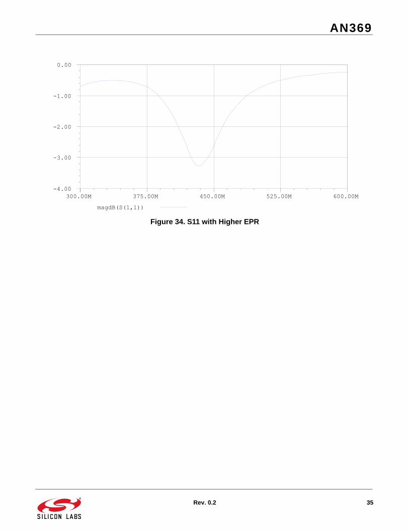
4. The balun function is checked when the RAP is replaced by the much higher EPR, i.e., the internal loss of the TX (TX_EPR). That is shown in Figure 33 assuming 20K EPR at cap. bank state 23. The balun function remained good, only the voltage magnitude increased in the same way at both differential nodes. The S11 becomes bad (Figure 34), but this is normal as described in Section “2. High Impedance Differential Power Amplifier”, in "voltage limited" mode when complex conjugate matching is not used for achieving the maximum power.
Figure 31. Simulated S11 of the MSOP Example
300.00M 375.00M 450.00M 525.00M 600.00M-40.00
-30.00
-20.00
-10.00
0.00
magdB(S(1,1))

AN369
34 Rev. 0.2
Figure 32. Voltage Transfer Function
Figure 33. Voltage Transfer Function with Higher EPR
300.00M 375.00M 450.00M 525.00M 600.00M0.00
0.63
1.25
1.88
2.50
-180.0
-90.00
0.00
90.00
180.0
PHASE
Mag(vac(o1)) Pha(vac(o1))Mag(vac(o2)) Pha(vac(o2))
300.00M 375.00M 450.00M 525.00M 600.00M0.00
1.00
2.00
3.00
4.00
-180.0
-90.00
0.00
90.00
180.0
PHASE
Mag(vac(o1)) Pha(vac(o1))Mag(vac(o2)) Pha(vac(o2))
AN369
Rev. 0.2 35
Figure 34. S11 with Higher EPR
300.00M 375.00M 450.00M 525.00M 600.00M-4.00
-3.00
-2.00
-1.00
0.00
magdB(S(1,1))

DisclaimerSilicon Laboratories intends to provide customers with the latest, accurate, and in-depth documentation of all peripherals and modules available for system and software implementers using or intending to use the Silicon Laboratories products. Characterization data, available modules and peripherals, memory sizes and memory addresses refer to each specific device, and "Typical" parameters provided can and do vary in different applications. Application examples described herein are for illustrative purposes only. Silicon Laboratories reserves the right to make changes without further notice and limitation to product information, specifications, and descriptions herein, and does not give warranties as to the accuracy or completeness of the included information. Silicon Laboratories shall have no liability for the consequences of use of the information supplied herein. This document does not imply or express copyright licenses granted hereunder to design or fabricate any integrated circuits. The products must not be used within any Life Support System without the specific written consent of Silicon Laboratories. A "Life Support System" is any product or system intended to support or sustain life and/or health, which, if it fails, can be reasonably expected to result in significant personal injury or death. Silicon Laboratories products are generally not intended for military applications. Silicon Laboratories products shall under no circumstances be used in weapons of mass destruction including (but not limited to) nuclear, biological or chemical weapons, or missiles capable of delivering such weapons.
Trademark InformationSilicon Laboratories Inc., Silicon Laboratories, Silicon Labs, SiLabs and the Silicon Labs logo, CMEMS®, EFM, EFM32, EFR, Energy Micro, Energy Micro logo and combinations thereof, "the world’s most energy friendly microcontrollers", Ember®, EZLink®, EZMac®, EZRadio®, EZRadioPRO®, DSPLL®, ISOmodem ®, Precision32®, ProSLIC®, SiPHY®, USBXpress® and others are trademarks or registered trademarks of Silicon Laboratories Inc. ARM, CORTEX, Cortex-M3 and THUMB are trademarks or registered trademarks of ARM Holdings. Keil is a registered trademark of ARM Limited. All other products or brand names mentioned herein are trademarks of their respective holders.
http://www.silabs.com
Silicon Laboratories Inc.400 West Cesar ChavezAustin, TX 78701USA
Simplicity StudioOne-click access to MCU tools, documentation, software, source code libraries & more. Available for Windows, Mac and Linux!
www.silabs.com/simplicity
MCU Portfoliowww.silabs.com/mcu
SW/HWwww.silabs.com/simplicity
Qualitywww.silabs.com/quality
Support and Communitycommunity.silabs.com