Si Photonics Technology Platform for Speed Optical … 2012 - Luxtera Proprietary Si Photonics...
23
www.luxtera.com ECOC 2012 - Luxtera Proprietary Si Photonics Technology Platform for High‐Speed Optical Interconnect Peter De Dobbelaere 9/17/2012
Transcript of Si Photonics Technology Platform for Speed Optical … 2012 - Luxtera Proprietary Si Photonics...

www.luxtera.comECOC 2012 - Luxtera Proprietary
Si Photonics Technology Platform for High‐Speed Optical Interconnect
Peter De Dobbelaere9/17/2012

• Luxtera: Introduction
• Silicon Photonics: Introduction
• Silicon Photonics: How it works
• Silicon Photonics: How it Scales to address customer’s needs
Overview
10/4/2012Page 2ECOC 2012 – Luxtera Proprietary

Luxtera is widely recognized as the industry Leader in Silicon Photonics− World’s only complete Si Photonics technology platform − Enables single‐chip multiple channel optical transceivers & full SoC integration
− Proven in Volume Production with over 1Mu 10Gb channels− Sustainable advantages on scalability, density, power, reach, reliability and product cost
Luxtera Company Overview
First to Commercially Deploy Silicon CMOS Photonics in Volume Products
10/4/2012Page 3ECOC 2012 – Luxtera Proprietary

• Luxtera’s Market Focus: Embedded Optics for Data Center, Cloud, Mobile Infrastructure and HPC Equipment − High volume embedded optical transceivers for backplanes, networking and high density interconnect
• Luxtera’s Product Portfolio: Optoelectronic transceiver chipsets, modules & IP cores for SoCintegration− Chip‐sets: Silicon Photonics Transceiver ICs and companion Light Sources
− OptoPhy™: Packaged optical transceivers modules− Circuit IP for stand alone transceivers and SoC integration
Luxtera Market Focus & Products
10/4/2012Page 4ECOC 2012 – Luxtera Proprietary

www.luxtera.comECOC 2012 - Luxtera Proprietary
Silicon Photonics: Introduction

Leverage the vast investments in CMOS technology to achieve low‐cost and high‐volume capability for photonics:• Process capability • High level of integration • High level of automation
IC industry methodologies adapted by Luxtera:• Design– Automated Design using standard design tools and qualified Opto‐Electronic Design Kit (device libraries, design rules,…)
– Extensive design verification prior to tape‐out
• Manufacturing– Emphasis on manufacturability– Process monitoring and control– Quality & Reliability
Si Photonics ‐ Luxtera
10/4/2012Page 6ECOC 2012 – Luxtera Proprietary
300 mm Si Photonics Wafer

Wafer manufacturing processes:• Mature 200 mm process: at Freescale Semiconductor (Austin, TX)Soon available through OpSIS
• Developing 300 mm process at ST Microelectronics (Crolles, France)
Wafer process allows:• Integration of Passive Devices• Integration of Active devices• Integration of Photo‐detectors• Integration of Electronics
Si Photonics – Luxtera: Wafer Processes
10/4/2012Page 7ECOC 2012 – Luxtera Proprietary
Fully Integrated transceiver IC

• Silicon Photonics Design Kit running on Cadence toolset
• Electronic and Photonic Device Library: ‐ Parameterized cells‐ Behavioral models built and
verified‐ Represent actual process corners
• Automated layout tools• Design Rule Check (DRC): Process/Device checks + interaction with electronics
• Layout vs Schematic (LVS) Check: E‐to‐E, E‐to‐O, and O‐to‐O connectivity and device extraction
• End‐to‐end simulation capability
Silicon Photonics – Luxtera: Design Environment
10/4/2012Page 8ECOC 2012 – Luxtera Proprietary

www.luxtera.comECOC 2012 - Luxtera Proprietary
Silicon Photonics:How it works

Optical I/O through grating couplers:• Coupling light form light source into die through matched grating coupler• Coupling TX signals out of die through SMF matched grating coupler • Coupling RX signals from SMF into die through polarization diversity grating coupler
Coupling Light In and Out of a Si Photonics Die
10/4/2012Page 10ECOC 2012 – Luxtera Proprietary
Light Source
Fiber Array
Si P Chip

Wafer‐Scale Optical and Electro‐Optical Testing
• System based on standard TEL Precioprobing system
• Allows 200 mm and 300 mm Silicon Photonics wafer testing
• Wafer‐scale testing is key for manufacturing and development
10/4/2012Page 11ECOC 2012 – Luxtera Proprietary

IC Functional Blocks:‐ TX: multi‐section MZI driven by invertors timed by digital delays, integrated bias control
‐ RX: Ge WPD with high impedance gain stages
‐ Programmable pre‐emphasis and equalization
‐ I2C interface for communication and control
4x28 G Transceiver IC Performance:‐ Error Free: BER<10‐15‐ Interoperability with 26‐28 G high speed IOs: Altera, Xilinx, Inphi, Gennum (OIF) and others
Technology Platform: 100Gb IC (4‐Ch 28Gb Transceiver)
10/4/2012Page 12ECOC 2012 – Luxtera Proprietary
Distributed MZIs and Calibration Circuit
SFP Out
Receivers
Optical Outputs
Optical Inputs
SFP In
Digital Control
Laser Driver
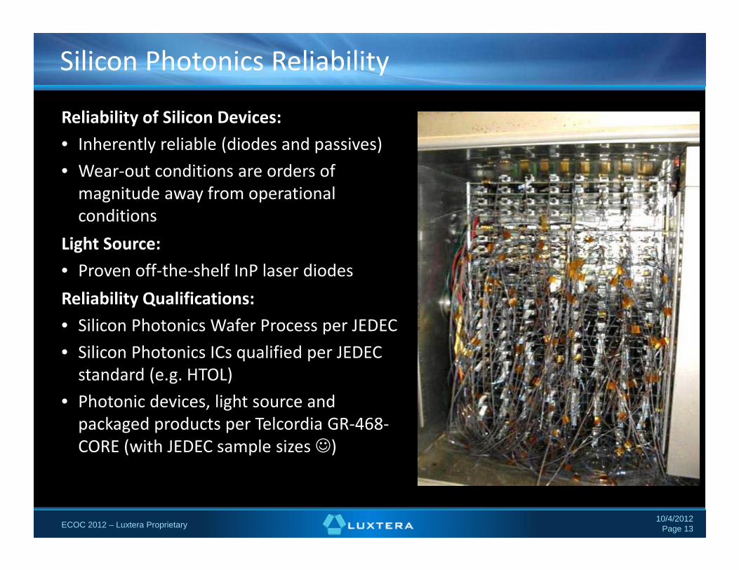
Reliability of Silicon Devices:• Inherently reliable (diodes and passives)• Wear‐out conditions are orders of magnitude away from operational conditions
Light Source:• Proven off‐the‐shelf InP laser diodesReliability Qualifications:• Silicon Photonics Wafer Process per JEDEC• Silicon Photonics ICs qualified per JEDEC standard (e.g. HTOL)
• Photonic devices, light source and packaged products per Telcordia GR‐468‐CORE (with JEDEC sample sizes )
Silicon Photonics Reliability
10/4/2012Page 13ECOC 2012 – Luxtera Proprietary

www.luxtera.comECOC 2012 - Luxtera Proprietary
Silicon Photonics:How it scales

• High‐Speed Phase Modulator– Intrinsic modulation bandwidth limited by relaxation time ~ 160 GHz
– Practical limit based on RC time • Drive signal rise time 1 ps• Rise time optical signal: ~ 5 ps
• High‐Speed Waveguide Photo‐Detector– Transit time limited bandwidth– Measured electrical (20.log[Iphoto]) bandwidth f0 > 50 GHz
• Electronics– Advanced CMOS nodes will be needed for the electronic circuitry (20 nm)
• Enables e.g. 64G Fibre Channel
Si P is Scalable to Data Rates beyond 56 Gbps NRZ
10/4/2012Page 15ECOC 2012 – Luxtera Proprietary

Si P is Scalable to Long Interconnect Reaches
10/4/2012Page 16ECOC 2012 – Luxtera Proprietary
100m 10km
SR4 LR4CR4
5m
300m 10km
SR LR ERCR
15m 40km
Cost optimized 100‐500m solution is critical to success of 100G!
ER4
Used by permission:Donn Lee, Facebook
• 100G needed for spines, not rack top switches• Reach from rack‐top to spine switch is 50‐500m• Overall cost is dominated by cost of optics• High port density per 1U is desirable• Customers will deploy the lowest cost solution that meets their requirements
100G
b (4x25)
10Gb
Enabled by Si Photonics single mode infrastructure and light source

• PAM‐N under consideration in IEEE standard study groups as low‐cost alternative to WDM (LR‐4) for 100 GbE
• Si Photonics is ideally suited for PAM‐N modulation • Integrated systems enable performance/power/size optimizations
− Entire functionality can be integrated into a single transceiver chipset
Si P is Scalable in Density: PAM‐N
Example PAM‐8 TX‐Eye:• 12 ps Rise/Fall Time• 8 dB Extinction Ratio
10/4/2012Page 17ECOC 2012 – Luxtera Proprietary
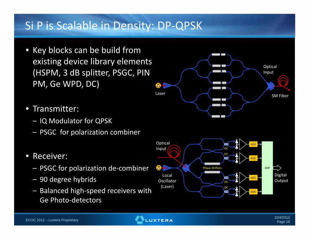
• Key blocks can be build from existing device library elements (HSPM, 3 dB splitter, PSGC, PIN PM, Ge WPD, DC)
• Transmitter:– IQ Modulator for QPSK– PSGC for polarization combiner
• Receiver:– PSGC for polarization de‐combiner– 90 degree hybrids– Balanced high‐speed receivers with Ge Photo‐detectors
Si P is Scalable in Density: DP‐QPSK
10/4/2012Page 18ECOC 2012 – Luxtera Proprietary

• Multiple fiber manufacturers explore multicore fibers with excellent results• Key issue is how to couple light in and out of MCF• Silicon photonics grating couplers are ideally suited for use with MCF allowing very dense optical interconnect
• MCF in combination with grating couplers allows 100s of optical interfaces on a single die.
Si P is Scalable in Density: Multi‐Core Fiber (MCF)
Silicon Photonics grating coupler arrangement 4 TX 4 RX
Cross section 8 core MCF 8 core MCF Array
10/4/2012Page 19ECOC 2012 – Luxtera Proprietary

Integration of Photonics with Router/Switch
10/4/2012Page 20ECOC 2012 – Luxtera Proprietary

Luxtera’s Photonic Integration Roadmap
CONTEMPORARY:• MSA compliant Pluggable modules and AOCs: QSFP, CXP,…
• Considerable SI issues (electrical connectors, long traces on host PCBA)
EMERGING:• Embedded Optical Modules• Located closer to ASIC to alleviate SI issues (shorter traces)
• Very high reliability requiredSTRATEGIC DIRECTION:• Si Photonic Interposer• SoC Integration• Smallest form factor• Lowest system power dissipation• Very high reliability required• Use external light source
System Level Power Dissipation per 100 G Port
10/4/2012Page 21ECOC 2012 – Luxtera Proprietary

• Silicon Photonics:− Leverages IC design and manufacturing methodologies − Is a mature technology in volume production
• Silicon photonics technology roadmap:− High NRZ data rates w/ long reach: 28 Gbps, 56 Gbps,…− Low power: Advanced CMOS Nodes & Integration− Higher density: PAM‐N, WDM, MCF, DP‐QPSK
• ASIC integration by Silicon Photonic Interposer enables dramatic reduction in system power, size and cost
Summary
10/4/2012Page 22ECOC 2012 – Luxtera Proprietary
This presentation is the work of the Luxtera team members, their contributions are greatly acknowledged.
Thank you for your interest.
Acknowledgements
10/4/2012Page 23ECOC 2012 – Luxtera Proprietary