shenzhen boxing world technology co.,ltd
26
PRODUCT NO.: PSP27801 PRODUCT NAME: PS11096096FR013 - 1 - REV.: A01 2013/10/16 Specification for Approval CUSTOMER APPROVED BY DATE: SHENZHEN BOXING WORLD TECHNOLOGY CO.,LTD
Transcript of shenzhen boxing world technology co.,ltd
PRODUCT NO.: PSP27801
PRODUCT NAME: PS11096096FR013
- 1 - REV.: A01 2013/10/16
Specification for Approval
CUSTOMER
APPROVED BY
DATE:
SHENZHEN BOXING WORLD TECHNOLOGY CO.,LTD
- 2 - REV.: A01 2013/10/16
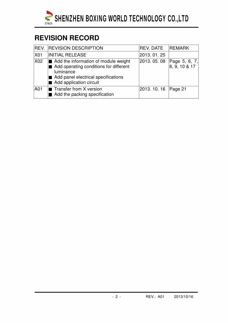
REVISION RECORD
REV. REVISION DESCRIPTION REV. DATE REMARK
X01 INITIAL RELEASE 2013. 01. 25
X02 ■ Add the information of module weight ■ Add operating conditions for different luminance ■ Add panel electrical specifications ■ Add application circuit
2013. 05. 08 Page 5, 6, 7, 8, 9, 10 & 17
A01 ■ Transfer from X version ■ Add the packing specification 2013. 10. 16 Page 21
SHENZHEN BOXING WORLD TECHNOLOGY CO.,LTD

- 3 - REV.: A01 2013/10/16
CONTENTS
ITEM PAGE
1. SCOPE 4
2. WARRANTY 4
3. FEATURES 4
4. MECHANICAL DATA 5
5. MAXIMUM RATINGS 6
6. ELECTRICAL CHARACTERISTICS 8
6.1 D.C ELECTRICAL CHARACTERISTICS 6.2 ELECTRO-OPTICAL CHARACTERISTICS
7. INTERFACE 11
7.1 FUNCTION BLOCK DIAGRAM
7.2 PANEL LAYOUT DIAGRAM 7.3 PIN ASSIGNMENTS 7.4 GRAPHIC DISPLAY DATA RAM ADDRESS MAP 7.5 INTERFACE TIMING CHART
8. POWER ON / OFF SEQUENCE & APPLICATION CIRCUIT 16
8.1 POWER ON / OFF SEQUENCE 8.2 APPLICATION CIRCUIT
8.3 COMMAND TABLE
9. RELIABILITY TEST CONDITIONS 18
10. EXTERNAL DIMENSION 19
11. PACKING SPECIFICATION 21
12. APPENDIXES 22
SHENZHEN BOXING WORLD TECHNOLOGY CO.,LTD

P&S
- 4 - REV.: A01 2013/10/16
1. SCOPE
The purpose of this specification is to define the general provisions and quality
requirements that apply to the supply of display cells manufactured by
Ass’y Drawing, is the
highest-level specification for this product. It describes the product, identifies
supporting documents and contains specifications.
2. WARRANTY
suant to this specification (or
order) will conform to the agreed specifications for twelve (12) months from the
ligated to repair or replace
the products which are found to be defective or inconsistent with the
specifications during the Warranty Period without charge, on condition that the
products are stored or used as the conditions specified in the specifications.
or replace the products
without charge if the defects or inconsistency are caused by the force majeure
or the reckless behaviors of the customer.
After the Warranty Period, all repairs or replacements of the products are
subject to charge.
3. FEATURES
‐ Small molecular organic light emitting diode.
‐ Color : 262K color and 65K colors
‐ Panel matrix : 96x96
‐ Driver IC : SSD1351
‐ Excellent quick response time.
‐ Extremely thin thickness for best mechanism design : 1.227mm
‐ High contrast : 2000:1
‐ Wide viewing angle : 160°
‐ 8/16-bit 8080-series Parallel Interface, Serial Peripheral Interface.
‐ Wide range of operating temperature : -40 to 70 °C
‐ Anti-glare polarizer.
warrants that the products delivered pur
This document, together with the Module
shipping date ("Warranty Period"). is ob
Nevertheless, is not obligated to repair
SHENZHEN BOXING WORLD TECHNOLOGY CO.,LTD
P&S
P&S
P&S
- 5 - REV.: A01 2013/10/16
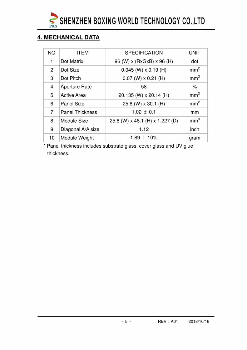
4. MECHANICAL DATA
NO ITEM SPECIFICATION UNIT
1 Dot Matrix 96 (W) x (RxGxB) x 96 (H) dot
2 Dot Size 0.045 (W) x 0.19 (H) mm2
3 Dot Pitch 0.07 (W) x 0.21 (H) mm2
4 Aperture Rate 58 %
5 Active Area 20.135 (W) x 20.14 (H) mm2
6 Panel Size 25.8 (W) x 30.1 (H) mm2
7 Panel Thickness 1.02 ± 0.1 mm
8 Module Size 25.8 (W) x 48.1 (H) x 1.227 (D) mm3
9 Diagonal A/A size 1.12 inch
10 Module Weight 1.89 ± 10% gram
* Panel thickness includes substrate glass, cover glass and UV glue
thickness.
SHENZHEN BOXING WORLD TECHNOLOGY CO.,LTD

- 6 - REV.: A01 2013/10/16
5. MAXIMUM RATINGS
ITEM MIN MAX UNIT Condition Remark
Supply Voltage (VCI) -0.3 4 V Ta = 25°C IC maximum
rating
Supply Voltage (Vcc) 10 21 V Ta = 25°C IC maximum
rating
Operating Temp. -40 70 °C
Storage Temp -40 85 °C
Humidity - 85 %
Life Time 10,000 - Hrs 100 cd/m², 50%
checkerboard Note (1)
Life Time 13,000 - Hrs 80 cd/m², 50%
checkerboard Note (2)
Life Time 16,000 - Hrs 60 cd/m², 50%
checkerboard Note (3)
Note:
(A) Under Vcc =15V, Ta = 25°C, 50% RH.
(B) Life time is defined the amount of time when the luminance has decayed
to less than 50% of the initial measured luminance.
(1) Setting of 100 cd/m2 :
- Master contrast setting : 0x0e
- Blue contrast setting : 0x75
- Green contrast setting : 0x42
- Red contrast setting : 0x49
- Frame rate : 105Hz
- Duty setting : 1/96
(2) Setting of 80 cd/m2 :
- Master contrast setting : 0x0c
- Blue contrast setting : 0x6b
- Green contrast setting : 0x3c
- Red contrast setting : 0x42
- Frame rate : 105Hz
- Duty setting : 1/96
SHENZHEN BOXING WORLD TECHNOLOGY CO.,LTD

- 7 - REV.: A01 2013/10/16
(3) Setting of 60 cd/m2 :
- Master contrast setting : 0x09
- Blue contrast setting : 0x68
- Green contrast setting : 0x3b
- Red contrast setting : 0x40
- Frame rate : 105Hz
- Duty setting : 1/96
SHENZHEN BOXING WORLD TECHNOLOGY CO.,LTD

- 8 - REV.: A01 2013/10/16
6. ELECTRICAL CHARACTERISTICS
6.1 D.C ELECTRICAL CHARACTERISTICS
SYMBOL PARAMETERS TEST
CONDITION MIN TYP MAX UNIT
VCC Analog power supply (for OLED panel)
14.5 15 15.5 V
VCI Digital power supply 2.4 2.8 3.5 V
VDDIO I/O voltage power supply 1.65 1.8 VCI V
IDD VCI = VDDIO =3.5V, VCC = 16V, External VDD = 2.6V, Display ON, No panel attached, contrast = FF
170 190 uA
External VDD = 2.6V
0.5 10 uA IDDIO
VCI = VDDIO =, 3.5V, VCC = 16V, Display ON, No panel attached, contrast = FF
Internal VDD 0.5 10 uA
External VDD = 2.6V
- 60 70 uA ICI
VCI = VDDIO =, 3.5V, VCC = 16V, Display ON, No panel attached, contrast = FF
Internal VDD 255 280 uA
External VDD = 2.6V
- 1.15 1.26 mA ICC
VCI = VDDIO =, 3.5V, VCC = 16V, Display ON, No panel attached, contrast = FF
Internal VDD 1.15 1.26 mA
VIH Hi logic input level 0.8* VDDIO
- VDDIO V
VIL Low logic input level 0 - 0.2* VDDIO
V
VOH Hi logic output level 0.9* VDDIO
- VDDIO V
VOL Low logic output level 0 - 0.1* VDDIO
V
Contrast=FF - 200 - uA
Contrast=7F - 100 - uA ISEG
Segment Output Current Setting VCC = 16V at IREF = 12.5uA Contrast=3F - 50 - uA
SHENZHEN BOXING WORLD TECHNOLOGY CO.,LTD

- 9 - REV.: A01 2013/10/16
6.2 ELECTRO-OPTICAL CHARACTERISTICS
PANEL ELECTRICAL SPECIFICATIONS
PARAMETER MIN TYP. MAX UNITS COMMENTS Normal mode current 16 18 mA All pixels on (1)
Standby mode current 6.5 8.5 mA Standby mode
10% pixels on (2)
Normal mode power consumption
240 270 mW All pixels on (1)
Standby mode power consumption
97.5 127.5 mW Standby mode
10% pixels on (2) Normal mode Luminance
60 80 cd/m2 Display Average
Standby mode Luminance
20 cd/m2
CIEx (White) 0.24 0.28 0.32 CIEy (White) 0.28 0.32 0.36
CIEx (Red) 0.62 0.66 0.70 CIEy (Red) 0.29 0.33 0.37 CIEx (Green) 0.26 0.30 0.34 CIEy (Green) 0.59 0.63 0.67 CIEx (Blue) 0.10 0.14 0.18 CIEy (Blue) 0.14 0.18 0.22
x, y (CIE 1931)
Dark Room Contrast 2000:1 Viewing Angle 160 degree Response Time 10 µs
(1) Normal mode condition :
- Driving Voltage : 15V
- Master contrast setting : 0x0c
- Blue contrast setting : 0x6b
- Green contrast setting : 0x3c
- Red contrast setting : 0x42
- Frame rate : 105Hz
- Duty setting : 1/96
SHENZHEN BOXING WORLD TECHNOLOGY CO.,LTD

- 10 - REV.: A01 2013/10/16
(2) Standby mode condition :
- Driving Voltage : 15V
- Master contrast setting : 0x04
- Blue contrast setting : 0x61
- Green contrast setting : 0x38
- Red contrast setting : 0x3b
- Frame rate : 105Hz
- Duty setting : 1/96
SHENZHEN BOXING WORLD TECHNOLOGY CO.,LTD

- 11 - REV.: A01 2013/10/16
7. INTERFACE
7.1 FUNCTION BLOCK DIAGRAM
7.2 PANEL LAYOUT DIAGRAM
96 x 3 x 96
OLED Panel
SSD1351
VLSS VCC VCI
VDD
IREF
RES#
D/C#
CS#
BS0~BS1
R/W#
E/RD
D0~D15
C33 ~ C127
C32 ~ C126
SA16~SA111
SB16~SB111
SC16~SC111
VSL VDDIO
VCOMH VSS
SHENZHEN BOXING WORLD TECHNOLOGY CO.,LTD
- 12 - REV.: A01 2013/10/16
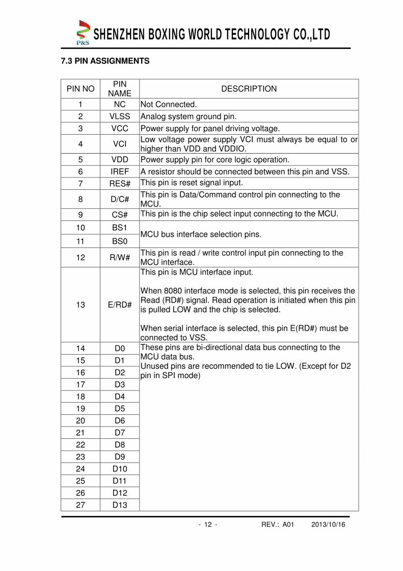
7.3 PIN ASSIGNMENTS
PIN NO PIN
NAME DESCRIPTION
1 NC Not Connected.
2 VLSS Analog system ground pin.
3 VCC Power supply for panel driving voltage.
4 VCI Low voltage power supply VCI must always be equal to or higher than VDD and VDDIO.
5 VDD Power supply pin for core logic operation.
6 IREF A resistor should be connected between this pin and VSS.
7 RES# This pin is reset signal input.
8 D/C# This pin is Data/Command control pin connecting to the MCU.
9 CS# This pin is the chip select input connecting to the MCU.
10 BS1
11 BS0 MCU bus interface selection pins.
12 R/W# This pin is read / write control input pin connecting to the MCU interface.
13 E/RD#
This pin is MCU interface input. When 8080 interface mode is selected, this pin receives the Read (RD#) signal. Read operation is initiated when this pin is pulled LOW and the chip is selected. When serial interface is selected, this pin E(RD#) must be connected to VSS.
14 D0
15 D1
16 D2
17 D3
18 D4
19 D5
20 D6
21 D7
22 D8
23 D9
24 D10
25 D11
26 D12
27 D13
These pins are bi-directional data bus connecting to the MCU data bus. Unused pins are recommended to tie LOW. (Except for D2 pin in SPI mode)
SHENZHEN BOXING WORLD TECHNOLOGY CO.,LTD

- 13 - REV.: A01 2013/10/16
28 D14
29 D15
30 VSL This is segment voltage reference pin. External VSL is set as default. This pin has to connect with resistor and diode to ground. (Details depend on application)
31 VDDIO Power supply for interface logic level.
32 VCOMH A capacitor should be connected between this pin and VSS.
33 VCC Power supply for panel driving voltage.
34 VSS Ground pin
SHENZHEN BOXING WORLD TECHNOLOGY CO.,LTD

- 14 - REV.: A01 2013/10/16
7.4 GRAPHIC DISPLAY DATA RAM ADDRESS MAP
The GDDRAM is a bit mapped static RAM holding the pattern to be displayed.
The RAM size is 128 x 128 x 18bits. For mechanical flexibility, re-mapping on
both Segment and Common outputs can be selected by software. Each pixel
has 18-bit data. Each sub-pixels for color A, B and C have 6 bits. The
arrangement of data pixel in graphic display data RAM is shown below.
SHENZHEN BOXING WORLD TECHNOLOGY CO.,LTD

- 15 - REV.: A01 2013/10/16
7.5 INTERFACE TIMING CHART
Note
(1) when 8 bit used: D[7:0] instead; when 16 bit used: [15:0] instead; when 18 bit
used: D[17:0] instead.
SHENZHEN BOXING WORLD TECHNOLOGY CO.,LTD

- 16 - REV.: A01 2013/10/16
8. POWER ON / OFF SEQUENCE & APPLICATION CIRCUIT
8.1 POWER ON / OFF SEQUENCE The following figures illustrate the recommended power ON and power OFF sequence of SSD1351
Power ON sequence: 1. Power ON VCI, VDDIO. 2. After VCI, VDDIO become stable, set wait time at least 1ms (t0) for internal VDD
become stable. Then set RES# pin LOW (logic low) for at least 2us (t1) (4) and
then HIGH (logic high). 3. After set RES# pin LOW (logic low), wait for at least 2us (t2). Then Power ON
VCC.(1) 4. After VCC become stable, send command AFh for display ON. SEG/COM will
be ON after 200ms(tAF).
Power OFF sequence: 1. Send command AEh for display OFF. 2. Power OFF VCC.(1), (2) 3. Wait for tOFF. Power OFF VCI, VDDIO.(where Minimum tOFF=80ms (3), Typical
tOFF=100ms)
Note:
(1) Since an ESD protection circuit is connected between VCI, VDDIO and VCC, VCC becomes lower
than VCI whenever VCI, VDDIO is ON and VCC is OFF as shown in the dotted line of VCC in Figure
(2)VCC should be kept float (disable) when it is OFF.
(3) VCI, VDDIO should not be Power OFF before VCC Power OFF.
(4) The register values are reset after t1.
(5) Power pins (VCI, VDDIO and VCC) can never be pulled to ground under any circumstance.
SHENZHEN BOXING WORLD TECHNOLOGY CO.,LTD
- 17 - REV.: A01 2013/10/16
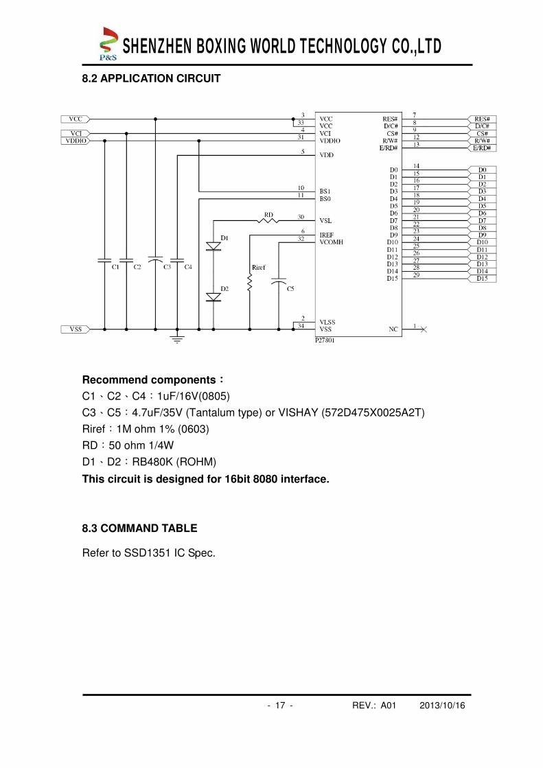
8.2 APPLICATION CIRCUIT
Recommend components::::
C1、C2、C4:1uF/16V(0805)
C3、C5:4.7uF/35V (Tantalum type) or VISHAY (572D475X0025A2T)
Riref:1M ohm 1% (0603)
RD:50 ohm 1/4W
D1、D2:RB480K (ROHM)
This circuit is designed for 16bit 8080 interface.
8.3 COMMAND TABLE
Refer to SSD1351 IC Spec.
SHENZHEN BOXING WORLD TECHNOLOGY CO.,LTD

- 18 - REV.: A01 2013/10/16
9. RELIABILITY TEST CONDITIONS
No. Items Specification Quantity
1 High temp. (Non-operation)
85°C, 240hrs 5
2 High temp. (Operation) 70°C, 120hrs 5
3 Low temp. (Operation) -40°C, 120hrs 5
4 High temp. / High humidity (Operation)
65°C, 90%RH, 96hrs 5
5 Thermal shock (Non-operation)
-40°C ~85°C (-40°C /30min; transit /3min; 85°C /30min; transit /3min) 1cycle: 66min, 20 cycles
5
6 Vibration
Frequency : 5~50HZ, 0.5G Scan rate : 1 oct/min Time : 2 hrs/axis Test axis : X, Y, Z
1 Carton
7 Drop
Height: 120cm Sequence : 1 angle、3 edges and
6 faces Cycles: 1
1 Carton
8 ESD (Non-operation) Air discharge model, ±8kV, 10 times
5
Test and measurement conditions
1. All measurements shall not be started until the specimens attain to
temperature stability.
2. All-pixels-on is used as operation test pattern.
3. The degradation of Polarizer are ignored for item 1, 4 & 5.
Evaluation criteria
1. The function test is OK.
2. No observable defects.
3. Luminance: > 50% of initial value.
4. Current consumption: within ± 50% of initial value.
SHENZHEN BOXING WORLD TECHNOLOGY CO.,LTD

PSP2
7801
PSP27801PSP27801

- 20 - REV.: A01 2013/10/16
SHENZHEN BOXING WORLD TECHNOLOGY CO.,LTD

PSP27801
PSP2
7801
PSP27801PSP27801

- 22 - REV.: A01 2013/10/16
12. APPENDIXES
APPENDIX 1: DEFINITIONS
A. DEFINITION OF CHROMATICITY COORDINATE
The chromaticity coordinate is defined as the coordinate value on the CIE
1931 color chart for R, G, B, W.
B. DEFINITION OF CONTRAST RATIO
The contrast ratio is defined as the following formula:
Luminance of all pixels on measurement Contrast Ratio =
Luminance of all pixels off measurement
C. DEFINITION OF RESPONSE TIME
The definition of turn-on response time Tr is the time interval between a pixel
reaching 10% of steady state luminance and 90% of steady state luminance.
The definition of turn-off response time Tf is the time interval between a pixel
reaching 90% of steady state luminance and 10% of steady state luminance.
It is shown in Figure 2.
Figure 2: Response time
1 0 %
T r T f
9 0 %
1 0 0 %
Bri
gh
tness
SHENZHEN BOXING WORLD TECHNOLOGY CO.,LTD
- 23 - REV.: A01 2013/10/16
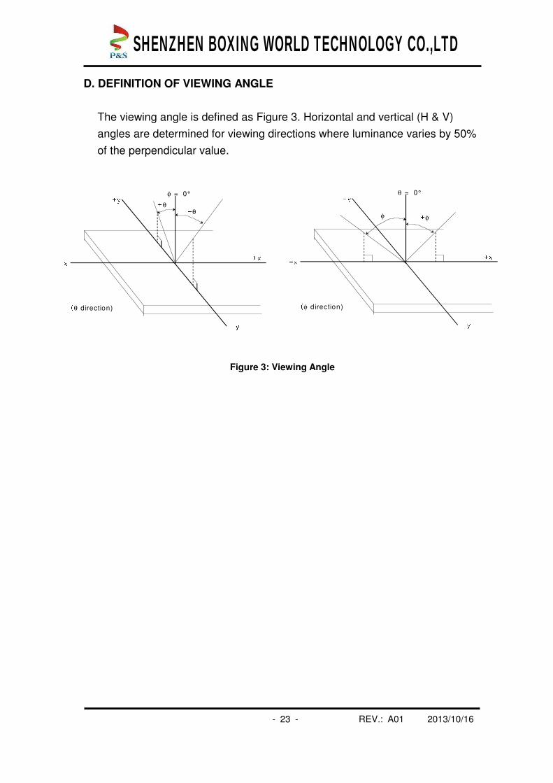
D. DEFINITION OF VIEWING ANGLE
The viewing angle is defined as Figure 3. Horizontal and vertical (H & V)
angles are determined for viewing directions where luminance varies by 50%
of the perpendicular value.
Figure 3: Viewing Angle
+θ -θ
φ = 0°+y-y
-x +x(θ direction)
+φ-φ
θ = 0°+y-y
-x +x(φ direction)
SHENZHEN BOXING WORLD TECHNOLOGY CO.,LTD

- 24 - REV.: A01 2013/10/16
PR-705 /
MINOLTA CS-100
Color Analyzer
Westar FPM-510
Display Contrast /
Response time /
View angle Analyzer
APPENDIX 2: MEASUREMENT APPARATUS
A. LUMINANCE/COLOR COORDINATE
PHOTO RESEARCH PR-705, MINOLTA CS-100
Measurement
Header
Panel
Plate Form
B. CONTRAST / RESPONSE TIME / VIEW ANGLE
WESTAR CORPORATION FPM-510
Measurement
Header
Panel
Plate Form
SHENZHEN BOXING WORLD TECHNOLOGY CO.,LTD

- 25 - REV.: A01 2013/10/16
C. ESD ON AIR DISCHARGE MODE
EUT
R 330 ohms
DISCHARGETIP
RETURN
C
150pF
ESD
GROUND PLANE
V
SHENZHEN BOXING WORLD TECHNOLOGY CO.,LTD

- 26 - REV.: A01 2013/10/16
APPENDIX 3: PRECAUTIONS
A. RESIDUE IMAGE
Because the pixels are lighted in different time, the luminance of active pixels
may reduce or differ from inactive pixels. Therefore, the residue image will
occur. To avoid the residue image, every pixel needs to be lighted up
uniformly.
SHENZHEN BOXING WORLD TECHNOLOGY CO.,LTD