SHD4102 - N-channel Power MOSFET Module...Figure 1. Q3: Safe Operating Area Figure 2. Q3: Power...
12
100 V, 10 A, 50 mΩ N-channel Power MOSFET Module SHD4102 Data Sheet SHD4102-DSE Rev.1.1 SANKEN ELCTRIC CO., LTD. 1 Oct. 31, 2018 https://www.sanken-ele.co.jp/en © SANKEN ELECTRIC CO., LTD. 2016 Description The SHD4102 includes four N-channel power MOSFETs in its small HSON package. The internal power MOSFETs have Zener diodes between gates and sources, thus requiring no externally clamped circuit for an injection coil drive circuit. Supplied in a low thermal resistance package, the product achieves high performance in heat dissipation. Features ● Suitable for High Reliability Applications ● Complies with Automotive Quality Requirements ● AEC-Q101 Qualified ● Bare Lead Frame: Pb-free (RoHS Compliant) ● Built-in Zener Diodes between Gates and Sources ● Low On-resistance ● Specifications (Q1 to Q4) V (BR)DSS --------------------------------- 100 V (I D = 100 μA) I D ---------------------------------------------------------- 10 A R DS(ON) ---------------- 50 mΩ max. (I D = 5 A, V GS = 10 V) Typical Application ● Solenoid Injection System DC/DC Control SHD4101 SHD4102 Package ● HSON-20 Not to scale Internal Schematic Diagram 10 8 12 15 17 13 S G G S 3 S G D G 5 7 20 Q1 1 4 D D D D 6 9 D 11 D D D 14 D 16 D D 19 S 18 Q2 Q3 Q4 2 D: Drain S: Source G: Gate Applications ● Injection Coil Driver Circuits
Transcript of SHD4102 - N-channel Power MOSFET Module...Figure 1. Q3: Safe Operating Area Figure 2. Q3: Power...

100 V, 10 A, 50 mΩ N-channel Power MOSFET Module
SHD4102 Data Sheet
SHD4102-DSE Rev.1.1 SANKEN ELCTRIC CO., LTD. 1 Oct. 31, 2018 https://www.sanken-ele.co.jp/en © SANKEN ELECTRIC CO., LTD. 2016
Description
The SHD4102 includes four N-channel power
MOSFETs in its small HSON package. The internal
power MOSFETs have Zener diodes between gates and
sources, thus requiring no externally clamped circuit for
an injection coil drive circuit. Supplied in a low thermal
resistance package, the product achieves high
performance in heat dissipation.
Features
● Suitable for High Reliability Applications
● Complies with Automotive Quality Requirements
● AEC-Q101 Qualified
● Bare Lead Frame: Pb-free (RoHS Compliant)
● Built-in Zener Diodes between Gates and Sources
● Low On-resistance
● Specifications (Q1 to Q4)
V(BR)DSS --------------------------------- 100 V (ID = 100 μA)
ID ---------------------------------------------------------- 10 A
RDS(ON) ---------------- 50 mΩ max. (ID = 5 A, VGS = 10 V)
Typical Application
● Solenoid Injection System
DC/DC
Control
SHD4101
SHD4102
Package
● HSON-20
Not to scale
Internal Schematic Diagram
10
8
12
15
17
13
S
GG
S
3
S
G
D
G 5
7
20
Q1
1 4
D D D
D6
9 D
11DDD
14D
16D
D 19
S 18
Q2
Q3Q4
2
D: Drain
S: Source
G: Gate
Applications
● Injection Coil Driver Circuits
SHD4102
SHD4102-DSE Rev.1.1 SANKEN ELCTRIC CO., LTD. 2 Oct. 31, 2018 https://www.sanken-ele.co.jp/en © SANKEN ELECTRIC CO., LTD. 2016
Absolute Maximum Ratings
Unless otherwise specified, TA = 25 °C.
Parameter Symbol Conditions Rating Unit
Drain-to-Source Voltage VDS 100 V
Gate-to-Source Voltage VGS ±20 V
Continuous Drain Current ID TC = 25 °C 10 A
Pulsed Drain Current IDM t ≤ 30 µs, duty cycle ≤ 1 % 30 A
Single Pulse Avalanche Energy EAS
VDD = 14 V, L = 1.08 mH,
ID = 10 A, unclamped,
RG = 50 Ω;
see Figure 16
62.5 mJ
Avalanche Current IAS 10 A
Drain-to-Source dv/dt 1 dv/dt 1 See Figure 16 0.6 V/ns
Peak Diode Recovery dv/dt 2 dv/dt 2 See Figure 17 5 V/ns
Peak Diode Recovery di/dt di/dt See Figure 17 100 A/µs
Power Dissipation PD
TC = 25 °C, all elements operating;
mounted on an FR4 board (26 mm
× 36 mm × 1.66 mm) 1.7 W
TC = 25 °C, all elements operating;
with an infinite heatsink 80 W
Junction Temperature TJ 150 °C
Storage Temperature TSTG −55 to 150 °C
Thermal Characteristics
Parameter Symbol Conditions Min. Typ. Max. Unit
Thermal Resistance
(Junction-to-Case) RθJC
TC = 25 °C, all elements operating;
with an infinite heatsink — — 6.25 °C/W
SHD4102
SHD4102-DSE Rev.1.1 SANKEN ELCTRIC CO., LTD. 3 Oct. 31, 2018 https://www.sanken-ele.co.jp/en © SANKEN ELECTRIC CO., LTD. 2016
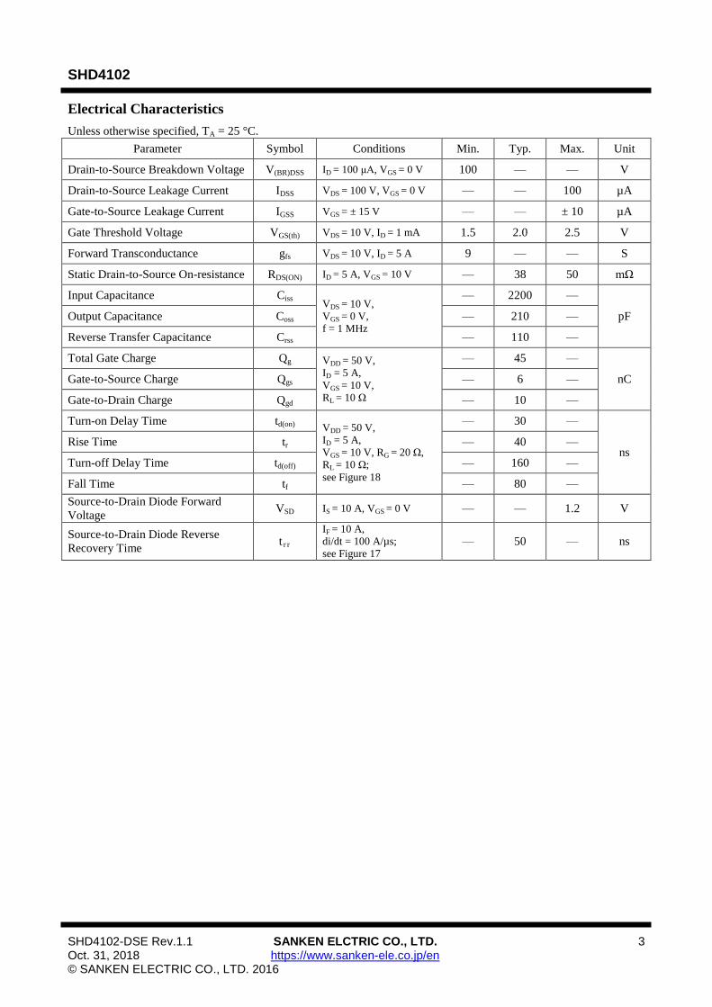
Electrical Characteristics
Unless otherwise specified, TA = 25 °C.
Parameter Symbol Conditions Min. Typ. Max. Unit
Drain-to-Source Breakdown Voltage V(BR)DSS ID = 100 μA, VGS = 0 V 100 — — V
Drain-to-Source Leakage Current IDSS VDS = 100 V, VGS = 0 V — — 100 µA
Gate-to-Source Leakage Current IGSS VGS = ± 15 V — — ± 10 µA
Gate Threshold Voltage VGS(th) VDS = 10 V, ID = 1 mA 1.5 2.0 2.5 V
Forward Transconductance gfs VDS = 10 V, ID = 5 A 9 — — S
Static Drain-to-Source On-resistance RDS(ON) ID = 5 A, VGS = 10 V — 38 50 mΩ
Input Capacitance Ciss VDS = 10 V,
VGS = 0 V,
f = 1 MHz
— 2200 —
pF Output Capacitance Coss — 210 —
Reverse Transfer Capacitance Crss — 110 —
Total Gate Charge Qg VDD = 50 V,
ID = 5 A,
VGS = 10 V,
RL = 10 Ω
— 45 —
nC Gate-to-Source Charge Qgs — 6 —
Gate-to-Drain Charge Qgd — 10 —
Turn-on Delay Time td(on) VDD = 50 V,
ID = 5 A,
VGS = 10 V, RG = 20 Ω,
RL = 10 Ω;
see Figure 18
— 30 —
ns Rise Time tr — 40 —
Turn-off Delay Time td(off) — 160 —
Fall Time tf — 80 —
Source-to-Drain Diode Forward
Voltage VSD IS = 10 A, VGS = 0 V — — 1.2 V
Source-to-Drain Diode Reverse
Recovery Time t r r
IF = 10 A,
di/dt = 100 A/µs;
see Figure 17 — 50 — ns
SHD4102
SHD4102-DSE Rev.1.1 SANKEN ELCTRIC CO., LTD. 4 Oct. 31, 2018 https://www.sanken-ele.co.jp/en © SANKEN ELECTRIC CO., LTD. 2016
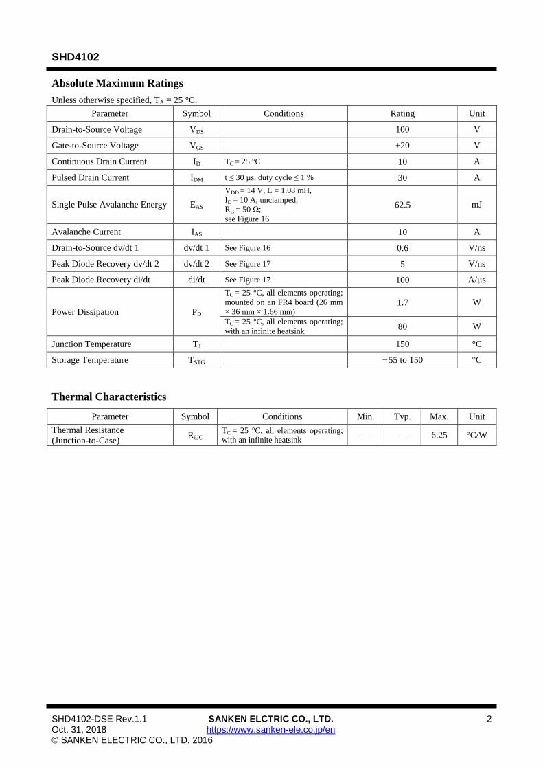
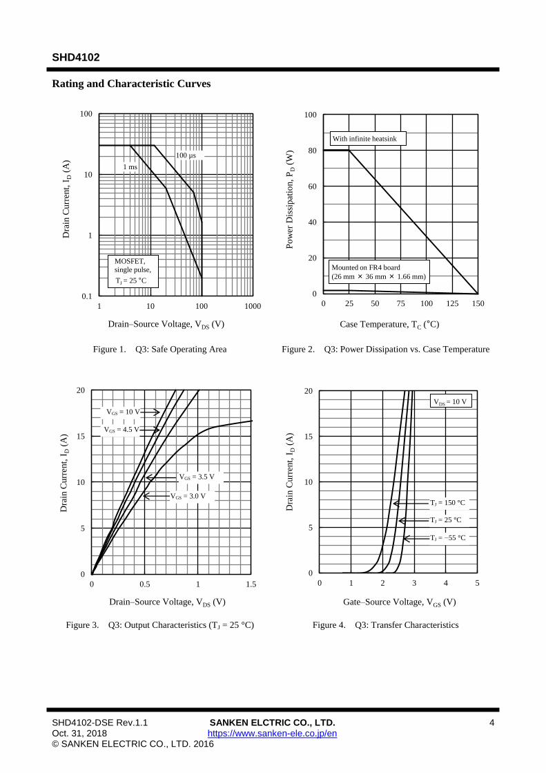
Rating and Characteristic Curves
Figure 1. Q3: Safe Operating Area Figure 2. Q3: Power Dissipation vs. Case Temperature
Figure 3. Q3: Output Characteristics (TJ = 25 °C) Figure 4. Q3: Transfer Characteristics
0.1
1
10
100
1 10 100 1000
Dra
in C
urr
ent,
ID (
A)
Drain–Source Voltage, VDS (V)
MOSFET,
single pulse,
TJ = 25 °C
0
20
40
60
80
100
0 25 50 75 100 125 150
Po
wer
Dis
sip
atio
n,
PD (
W)
Case Temperature, TC (°C)
With infinite heatsink
Mounted on FR4 board
(26 mm × 36 mm × 1.66 mm)
0
5
10
15
20
0 0.5 1 1.5
Dra
in C
urr
ent,
ID (
A)
Drain–Source Voltage, VDS (V)
0
5
10
15
20
0 1 2 3 4 5
Dra
in C
urr
ent,
ID (
A)
Gate–Source Voltage, VGS (V)
VDS = 10 V
100 µs
1 ms
VGS = 4.5 V
VGS = 10 V
TJ = −55 °C
TJ = 25 °C
TJ = 150 °C VGS = 3.0 V
VGS = 3.5 V

SHD4102
SHD4102-DSE Rev.1.1 SANKEN ELCTRIC CO., LTD. 5 Oct. 31, 2018 https://www.sanken-ele.co.jp/en © SANKEN ELECTRIC CO., LTD. 2016
Figure 5. Q3: Drain Current vs. Case Temperature Figure 6. Q3: Gate Threshold Voltage vs. Junction
Temperature
Figure 7. Q3: Drain–Source On-resistance vs. Drain
Current
Figure 8. Q3: Drain–Source On-resistance vs. Junction
Temperature
0
2
4
6
8
10
12
0 25 50 75 100 125 150
Dra
in C
urr
ent,
ID (
A)
Case Temperature, TC (°C)
0.5
1
1.5
2
2.5
-100 -50 0 50 100 150 200 G
ate
Th
resh
old
Vo
ltag
e,V
th (
V)
Junction Temperature, TJ (°C)
VDS = 10 V,
ID = 1 mA
0
10
20
30
40
50
60
0 5 10 15 20
Dra
in–
So
urc
e O
n-r
esis
tance
, R
DS
(on) (m
Ω)
Drain Current, ID (A)
VGS = 10 V,
TJ = 25 °C
0
20
40
60
80
100
-100 -50 0 50 100 150 200
Dra
in–
So
urc
e O
n-r
esis
tance
, R
DS
(on) (m
Ω)
Junction Temperature, TJ (°C)
VGS = 10 V,
ID = 5 A
SHD4102
SHD4102-DSE Rev.1.1 SANKEN ELCTRIC CO., LTD. 6 Oct. 31, 2018 https://www.sanken-ele.co.jp/en © SANKEN ELECTRIC CO., LTD. 2016
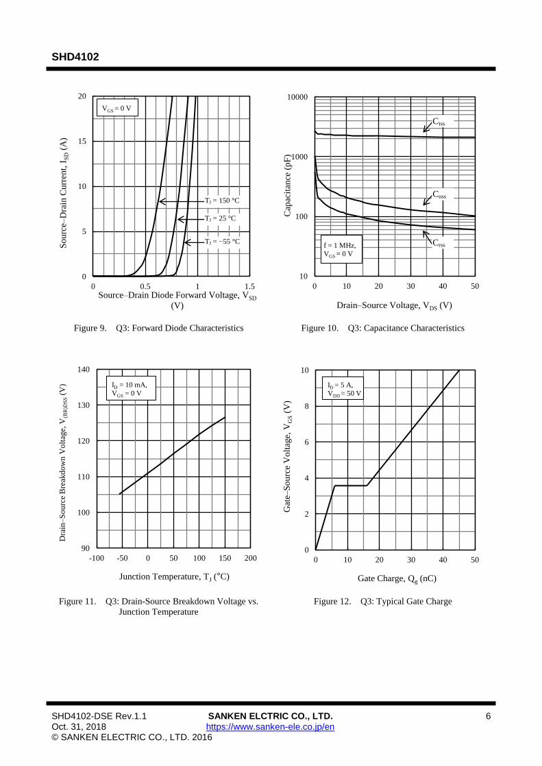
Figure 9. Q3: Forward Diode Characteristics Figure 10. Q3: Capacitance Characteristics
Figure 11. Q3: Drain-Source Breakdown Voltage vs.
Junction Temperature
Figure 12. Q3: Typical Gate Charge
0
5
10
15
20
0 0.5 1 1.5
So
urc
e–D
rain
Curr
ent,
IS
D (
A)
Source–Drain Diode Forward Voltage, VSD
(V)
VGS = 0 V
10
100
1000
10000
0 10 20 30 40 50 C
apac
itan
ce (
pF
)
Drain–Source Voltage, VDS (V)
f = 1 MHz,
VGS = 0 V
90
100
110
120
130
140
-100 -50 0 50 100 150 200
Dra
in–
So
urc
e B
reak
do
wn
Vo
ltag
e, V
(BR
)DS
S (
V)
Junction Temperature, TJ (°C)
ID = 10 mA,
VGS = 0 V
0
2
4
6
8
10
0 10 20 30 40 50
Gat
e–S
ourc
e V
olt
age,
VG
S (
V)
Gate Charge, Qg (nC)
ID = 5 A,
VDD ≈ 50 V
TJ = −55 °C
TJ = 25 °C
TJ = 150 °C
Ciss
Coss
Crss

SHD4102
SHD4102-DSE Rev.1.1 SANKEN ELCTRIC CO., LTD. 7 Oct. 31, 2018 https://www.sanken-ele.co.jp/en © SANKEN ELECTRIC CO., LTD. 2016
Figure 13. Q3: Typical Avalanche Energy Figure 14. Q3: Transfer Characteristics
Figure 15. Q3: Transient Thermal Resistance
0
10
20
30
40
50
60
70
25 50 75 100 125 150
Sin
gle
Puls
e A
val
anch
e E
ner
gy,
EA
S (
mJ)
Junction Temperature, TJ (°C)
0
0.2
0.4
0.6
0.8
1
0 5 10 15 20 D
rain
–S
ourc
e V
olt
age,
VD
S (
V)
Gate–Source Voltage, VGS (V)
VDS = 10 V
0.01
0.1
1
10
Ther
mal
Res
ista
nce
(°C
/W)
Pulse Width (s)
Single pulse,
VDS < 10 V
100 μ 1 m 10 m 100 m 1 10
ID = 10A
ID = 5A

SHD4102
SHD4102-DSE Rev.1.1 SANKEN ELCTRIC CO., LTD. 8 Oct. 31, 2018 https://www.sanken-ele.co.jp/en © SANKEN ELECTRIC CO., LTD. 2016
Test Circuits and Waveforms
v
VDD
ID
VDS
RG
VGS
0 V
L
VDS
ID
IAS
t
t
V(BR)DSS
VDD
dv/dt 1
(a) Test Circuit (b) Waveforms
Figure 16. Unclamped Inductive Test Circuit and Switching Time Waveforms
VGS
0 V
IF
RG
L
D.U.T.
VDD
0
IF
trr
di/dt
IRM × 90 %
IRM
0
VSD
VDD
dv/dt 2
(a) Test Circuit (b) Waveforms
Figure 17. Diode Reverse Recovery Time
VDS
VDDRG
RL
VGS
0 V
P.W. = 10 μs
Duty cycle ≤ 1 %
td(on) tr
ton
td(off) tf
toff
90%
10%
90%
10%
VGS
VDS
0
0
(a) Test Circuit (b) Waveforms
Figure 18. Resistive Load Test Circuit and Switching Time Waveforms
SHD4102
SHD4102-DSE Rev.1.1 SANKEN ELCTRIC CO., LTD. 9 Oct. 31, 2018 https://www.sanken-ele.co.jp/en © SANKEN ELECTRIC CO., LTD. 2016
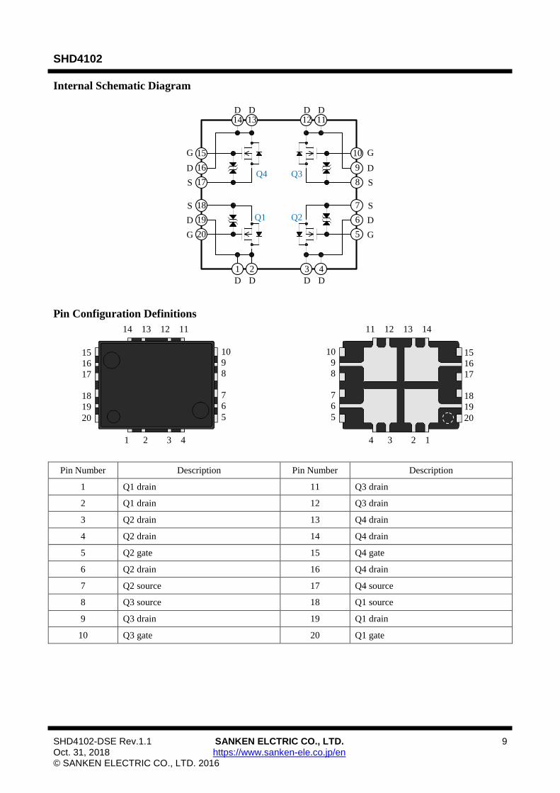
Internal Schematic Diagram
10
8
12
15
17
13
S
GG
S
3
S
G
D
G 5
7
20
Q1
1 4
D D D
D6
9 D
11DDD
14D
16D
D 19
S 18
Q2
Q3Q4
2
Pin Configuration Definitions
Pin Number Description Pin Number Description
1 Q1 drain 11 Q3 drain
2 Q1 drain 12 Q3 drain
3 Q2 drain 13 Q4 drain
4 Q2 drain 14 Q4 drain
5 Q2 gate 15 Q4 gate
6 Q2 drain 16 Q4 drain
7 Q2 source 17 Q4 source
8 Q3 source 18 Q1 source
9 Q3 drain 19 Q1 drain
10 Q3 gate 20 Q1 gate
1 2 3 4
14 13 12 11
10
9
8
7
6
5
15
16
17
18
19
20
4 3 2 1
11 12 13 14
10
9
8
7
6
5
15
16
17
18
19
20
SHD4102
SHD4102-DSE Rev.1.1 SANKEN ELCTRIC CO., LTD. 10 Oct. 31, 2018 https://www.sanken-ele.co.jp/en © SANKEN ELECTRIC CO., LTD. 2016
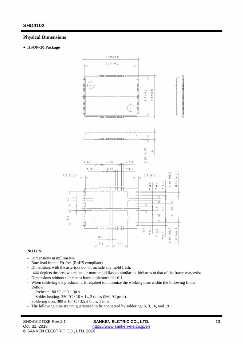
Physical Dimensions
● HSON-20 Package
±0.2
±0.2
±0.2
±0.2
0.25
1.5
2.140.4 0.4
4.680.4 0.4
0.8
3.6
0.4
0.4
5.6
0.8
0.8
0.7
3.3
3.3
0.7
3.3 3.3
0.8
0.8
*
*
*
*
**
*
* *
±0.05
11.3
11.9
8.5
9.1
*
0.5 (min.) 0.5 (min.)
0.55
(min.)
0.55
(min.)
0.55
(min.)
0.55
(min.)
NOTES:
- Dimensions in millimeters
- Bare lead frame: Pb-free (RoHS compliant)
- Dimensions with the asterisks do not include any mold flash.
- depicts the area where one or more mold flashes similar in thickness to that of the frame may exist.
- Dimensions without tolerances have a tolerance of ±0.1.
- When soldering the products, it is required to minimize the working time within the following limits:
Reflow
Preheat: 180 °C / 90 ± 30 s
Solder heating: 250 °C / 10 ± 1s, 2 times (260 °C peak)
Soldering iron: 380 ± 10 °C / 3.5 ± 0.5 s, 1 time
- The following pins are not guaranteed to be connected by soldering: 6, 9, 16, and 19.
SHD4102
SHD4102-DSE Rev.1.1 SANKEN ELCTRIC CO., LTD. 11 Oct. 31, 2018 https://www.sanken-ele.co.jp/en © SANKEN ELECTRIC CO., LTD. 2016
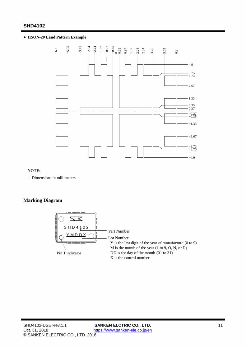
● HSON-20 Land Pattern Example
00.270.35
1.33
2.67
3.733.75
4.9
−0.27−0.35
−1.33
−2.67
−3.73−3.75
−4.9
6.3
5.0
5
3.7
5
2.8
4
2.2
4
1.5
7
0.9
7
0.3
50−
0.3
5
−0
.97
−1
.57
−2
.24
−2
.84
−3
.75
−5
.05
−6
.3
NOTE:
- Dimensions in millimeters
Marking Diagram
Part NumberS H D 4 1 0 2
Lot Number:
Y is the last digit of the year of manufacture (0 to 9)
M is the month of the year (1 to 9, O, N, or D)
DD is the day of the month (01 to 31)
X is the control number
Y M D D X
Pin 1 indicator

SHD4102
SHD4102-DSE Rev.1.1 SANKEN ELCTRIC CO., LTD. 12 Oct. 31, 2018 https://www.sanken-ele.co.jp/en © SANKEN ELECTRIC CO., LTD. 2016
Important Notes
● All data, illustrations, graphs, tables and any other information included in this document (the “Information”) as to Sanken’s
products listed herein (the “Sanken Products”) are current as of the date this document is issued. The Information is subject to any
change without notice due to improvement of the Sanken Products, etc. Please make sure to confirm with a Sanken sales
representative that the contents set forth in this document reflect the latest revisions before use.
● The Sanken Products are intended for use as components of electronic equipment or apparatus (transportation equipment and its
control systems, home appliances, office equipment, telecommunication equipment, measuring equipment, etc.). Prior to use of the
Sanken Products, please put your signature, or affix your name and seal, on the specification documents of the Sanken Products
and return them to Sanken. If considering use of the Sanken Products for any applications that require higher reliability (traffic
signal control systems or equipment, disaster/crime alarm systems, etc.), you must contact a Sanken sales representative to discuss
the suitability of such use and put your signature, or affix your name and seal, on the specification documents of the Sanken
Products and return them to Sanken, prior to the use of the Sanken Products. The Sanken Products are not intended for use in any
applications that require extremely high reliability such as: aerospace equipment; nuclear power control systems; and medical
equipment or systems, whose failure or malfunction may result in death or serious injury to people, i.e., medical devices in Class
III or a higher class as defined by relevant laws of Japan (collectively, the “Specific Applications”). Sanken assumes no liability or
responsibility whatsoever for any and all damages and losses that may be suffered by you, users or any third party, resulting from
the use of the Sanken Products in the Specific Applications or in manner not in compliance with the instructions set forth herein. ● In the event of using the Sanken Products by either (i) combining other products or materials or both therewith or (ii) physically,
chemically or otherwise processing or treating or both the same, you must duly consider all possible risks that may result from all
such uses in advance and proceed therewith at your own responsibility. ● Although Sanken is making efforts to enhance the quality and reliability of its products, it is impossible to completely avoid the
occurrence of any failure or defect or both in semiconductor products at a certain rate. You must take, at your own responsibility,
preventative measures including using a sufficient safety design and confirming safety of any equipment or systems in/for which
the Sanken Products are used, upon due consideration of a failure occurrence rate and derating, etc., in order not to cause any
human injury or death, fire accident or social harm which may result from any failure or malfunction of the Sanken Products.
Please refer to the relevant specification documents and Sanken’s official website in relation to derating. ● No anti-radioactive ray design has been adopted for the Sanken Products. ● The circuit constant, operation examples, circuit examples, pattern layout examples, design examples, recommended examples, all
information and evaluation results based thereon, etc., described in this document are presented for the sole purpose of reference of
use of the Sanken Products. ● Sanken assumes no responsibility whatsoever for any and all damages and losses that may be suffered by you, users or any third
party, or any possible infringement of any and all property rights including intellectual property rights and any other rights of you,
users or any third party, resulting from the Information. ● No information in this document can be transcribed or copied or both without Sanken’s prior written consent.
● Regarding the Information, no license, express, implied or otherwise, is granted hereby under any intellectual property rights and
any other rights of Sanken. ● Unless otherwise agreed in writing between Sanken and you, Sanken makes no warranty of any kind, whether express or implied,
including, without limitation, any warranty (i) as to the quality or performance of the Sanken Products (such as implied warranty
of merchantability, and implied warranty of fitness for a particular purpose or special environment), (ii) that any Sanken Product is
delivered free of claims of third parties by way of infringement or the like, (iii) that may arise from course of performance, course
of dealing or usage of trade, and (iv) as to the Information (including its accuracy, usefulness, and reliability). ● In the event of using the Sanken Products, you must use the same after carefully examining all applicable environmental laws and
regulations that regulate the inclusion or use or both of any particular controlled substances, including, but not limited to, the EU
RoHS Directive, so as to be in strict compliance with such applicable laws and regulations. ● You must not use the Sanken Products or the Information for the purpose of any military applications or use, including but not
limited to the development of weapons of mass destruction. In the event of exporting the Sanken Products or the Information, or
providing them for non-residents, you must comply with all applicable export control laws and regulations in each country
including the U.S. Export Administration Regulations (EAR) and the Foreign Exchange and Foreign Trade Act of Japan, and
follow the procedures required by such applicable laws and regulations. ● Sanken assumes no responsibility for any troubles, which may occur during the transportation of the Sanken Products including
the falling thereof, out of Sanken’s distribution network. ● Although Sanken has prepared this document with its due care to pursue the accuracy thereof, Sanken does not warrant that it is
error free and Sanken assumes no liability whatsoever for any and all damages and losses which may be suffered by you resulting
from any possible errors or omissions in connection with the Information. ● Please refer to our official website in relation to general instructions and directions for using the Sanken Products, and refer to the
relevant specification documents in relation to particular precautions when using the Sanken Products.
● All rights and title in and to any specific trademark or tradename belong to Sanken and such original right holder(s).
DSGN-AEZ-16003


![Q3 2019 Ordubad Techincal Summary WRA · Ordubad Technical Summary – Q3 2019 7 Figure 9 – A trace element plot for intrusive igneous rocks [6], with Ordubad samples overlain.](https://static.fdocuments.us/doc/165x107/5f9b8fb201247e5065343882/q3-2019-ordubad-techincal-summary-wra-ordubad-technical-summary-a-q3-2019-7-figure.jpg)