
Shaahin Hessabi Department of Computer Engineering...
21
Shaahin Hessabi Department of Computer Engineering Sharif University of Technology
Transcript of Shaahin Hessabi Department of Computer Engineering...

Shaahin HessabiDepartment of Computer Engineering
Sharif University of Technology
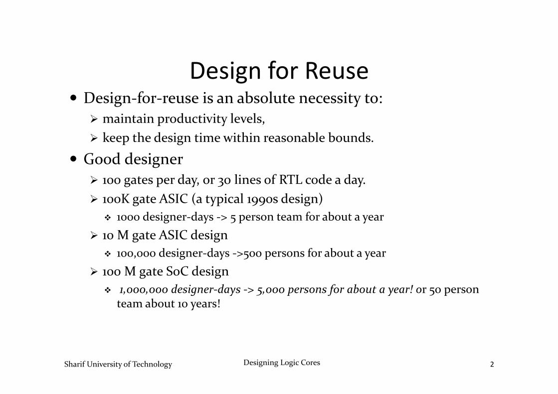
D i f RDesign for ReuseDesign‐for‐reuse is an absolute necessity to:
maintain productivity levels,keep the design time within reasonable bounds.
Good designer100 gates per day, or 30 lines of RTL code a day.100K gate ASIC (a typical 1990s design)100K gate ASIC (a typical 1990s design)
1000 designer‐days ‐> 5 person team for about a year10 M gate ASIC designg g
100,000 designer‐days ‐>500 persons for about a year100 M gate SoC design
d i d f b t ! 1,000,000 designer‐days ‐> 5,000 persons for about a year! or 50 person team about 10 years!
Sharif University of Technology Designing Logic Cores 2

Design for Reuse Requirementsd f l dgood functional documentation,
good coding practices,carefully designed verification environments
thorough test suites,
b d il EDA l irobust and versatile EDA tool scriptseffective porting mechanism across various technology libraries (for hard cores)libraries (for hard cores).
Sharif University of Technology Designing Logic Cores 3
General Guidelines for Design ReuseDesign Process for Soft and Firm CoresgDesign Process for Hard Cores
Sharif University of Technology Designing Logic Cores 4

General Guidelines for Design ReusehSynchronous Design
Memory and Mixed‐Signal DesignOn‐Chip BusesClock DistributionClear/Set/Reset SignalsDeliverable Models
Sharif University of Technology Designing Logic Cores 5
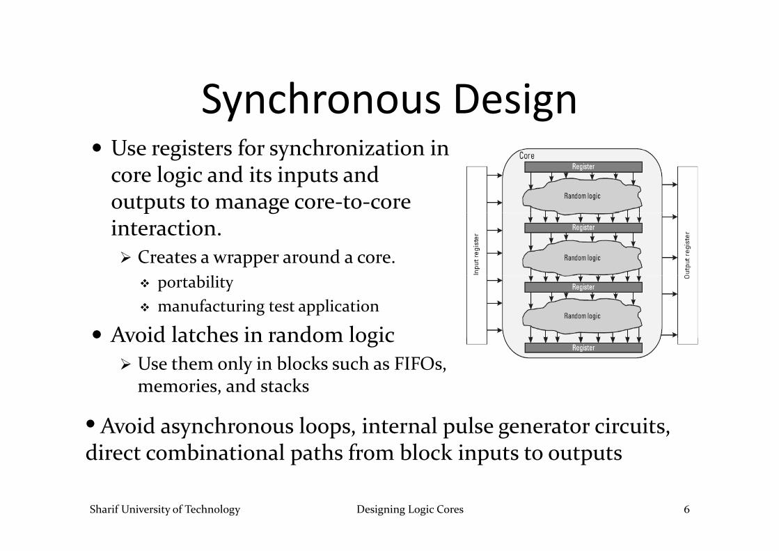
S h D iSynchronous DesignUse registers for synchronization in Use registers for synchronization in core logic and its inputs and outputs to manage core‐to‐core p ginteraction.
Creates a wrapper around a core.b lportability
manufacturing test application
Avoid latches in random logicAvoid latches in random logicUse them only in blocks such as FIFOs, memories, and stacks
• Avoid asynchronous loops, internal pulse generator circuits, direct combinational paths from block inputs to outputs
Sharif University of Technology Designing Logic Cores 6
p p p

Memory and Mixed‐Signal DesignLarge memories: different parasitics at boundary cells and a cell in the middle of an array.
Include rows and columns of dummy cells at the Include rows and columns of dummy cells at the periphery of large memoriesMake these rows and columns part of the built‐in self‐
( ) h h drepair (BISR) mechanism, to minimize area overhead.
most commonly used analog/mixed‐i l i it d i S C PLL signal circuits used in SoC: PLLs, ADCs/DACs, and temperature sensors.
extremely sensitive to noise and extremely sensitive to noise and technology parameters
place them at the corners
Sharif University of Technology Designing Logic Cores 7
On‐Chip BusesOn‐chip buses and data transaction protocol must be designed prior to the core selection process.Core providers cannot envision all possible interfaces.
Parameterized interfaces should be used in core design.FIFO b d i f fl ibl d il i h dli i d FIFO‐based interfaces are flexible and versatile in handling varying data rates between cores and the system buses
Organizations (VSI Alliance, …) develop on‐chip bus and g ( , ) p pcore interface standards/specifications.
support multiple masters, separate identity for data and control i l f ll h d l i l l i b signals, fully synchronous and multiple cycle transactions, bus request‐and‐grant protocol
Sharif University of Technology Designing Logic Cores 8

Clock Distributionh ll b f l k dUse the smallest number of clock domains.
Isolate each clock in an independent domain.Use buffers at the clock boundary.Avoid metastability between clock domains interface Use synchronization method at the clock boundaries.
E.g., clock buffering and dual stage FFs or FIFOs at the clock boundaryboundary.
Distribute a low‐frequency chip‐level synchronization clock when cores contain local PLLs. clock when cores contain local PLLs.
Each core’s local PLL should lock to this clock and generate required frequency for the core.
Sharif University of Technology Designing Logic Cores 9
Cl /S t/R t Si lClear/Set/Reset SignalsDocument all reset schemes for the entire design:Document all reset schemes for the entire design:
Synchronous/asynchronous, internal/external power‐on‐resets, any software reset schemes used,ydoes any functional block has locally generated resets,whether resets are synchronized with local clocks, …
Use synchronous reset if possibleavoids race conditions on reset,t ti ti i l i diffi lt ith h tstatic timing analysis difficult with asynchronous resets,designer has to evaluate the reset pulse width at every FF
to make sure it becomes inactive synchronously to clocksy y
Sharif University of Technology Designing Logic Cores 10

D li bl M d lDeliverable ModelsDesign reuse depends on quality of deliverable models:Design reuse depends on quality of deliverable models:
behavioral or instruction set architecture (ISA) model, bus functional model for system‐level verification, yfully functional model for timing and cycle‐based logic simulation/emulation,h i l d i d l fl l i ti i d physical design models: floor planning, timing, and area
Might be delivered in encrypted form to restrict piracy and reverse engineeringreverse engineering.
create a top‐level module and instantiate the core model inside it.the top‐level module behaves as a wrapper and hides the whole netlist, floor planning, and timing of the core
Sharif University of Technology Designing Logic Cores 11

D li bl M d l (N d d U )Deliverable Models (Need and Usage)
Sharif University of Technology Designing Logic Cores 12
Design Process for Soft and Firm CoreslDesign Flow
Development Process for Soft/Firm CoresRTL GuidelinesSoft/Firm Cores Deliverables
Sharif University of Technology Designing Logic Cores 13

Design FlowDesign with a conventional EDA RTL th i flRTL synthesis flow.Reusability requirement requirement multiple configuration tests should be developed and run.
Sharif University of Technology Designing Logic Cores 14
Development Process for Soft/Firm CoresRequired design specifications at every step in development Required design specifications at every step in development process:1. Functional (purpose and operation)p p p2. Physical (packaging, area, power, technology libraries, …)3. Design requirements (architecture and block diagrams with data
fl )flow)4. Interface requirements to specify signal names and functions, timing
diagrams, and DC/AC parametersg p5. Test and debug (testing, DFT methodology, test vector generation
method, fault grading, …)6 S ft i t ( ft d i d d l f h d 6. Software requirements (software drivers and models for hardware
blocks)
Sharif University of Technology Designing Logic Cores 15
RTL GuidelinesRTL coding style determines:g y
PortabilityReusabilityArea and performance of the core after synthesis.
So, develop RTL code that is:Simple and easy to understand,structured,uses simple constructs and consistent naming conventionsuses simple constructs and consistent naming conventionsEasy to verify and synthesize.
Consult Verilog/VHDL books for good coding guidelines.Co su t e og/ boo s o good cod g gu de es.
Sharif University of Technology Designing Logic Cores 16

Soft/Firm Cores Deliverablesd f lProduct filesSynthesizable source codeApplication notes with HDL design exampleApplication notes with HDL design exampleSynthesis scripts & timing constraintsScripts for scan insertion and ATPGpReference libraryInstallation scripts
Verification filesBus functional model/monitors used in testbenchT b h fil i l di i ifi i Testbench files including representative verification tests
Sharif University of Technology Designing Logic Cores 17

S f /Fi C D li bl ( ’d)Soft/Firm Cores Deliverables(cont’d)
DocumentationUser guide/Functional specificationDatasheetDatasheet
System integration files/toolsCycle‐based/emulation models as appropriate for macro and/or its Cycle based/emulation models as appropriate for macro and/or its testbenches and BFMsCompilers, debuggers, real‐time operating systems and software d i f bl IPdrivers for programmable processor IP
Additional for firm cores:gate le el netlist description of the technolog librar timing gate‐level netlist, description of the technology library, timing model, area, and power estimates.
Sharif University of Technology Designing Logic Cores 18
Design Process for Hard CoresClock and ResetClock and ResetPorosity, Pin Placement, and Aspect Ratio
Sharif University of Technology Designing Logic Cores 19
Cl k d RClock and ResetImplementation of clock and reset should be independent of SoC clock and reset.
Since SoC‐level information not available at the time of core design.
Clock and reset require buffering and minimum wire loading.Cl k t b il bl t t i f th Clock must be available on an output pin of the core.
Used for synchronization with other SoC‐level on‐chip clocks.
Sharif University of Technology Designing Logic Cores 20

Porosity, Pin Placement, and Aspect RatioDuring SoC‐level integration, often desirable to route over a g gcore or through a core.
Hard core should have porosity, i.e., some routing channels through the core should be made available; orthe core should be made available; orlimit number of metal layers in the core to 1‐2 less than the maximum allowable by the process.
D li bl f th h ld i l d bl k t id tif th Deliverables for the core should include a blockage map to identify the areas where SoC‐level routing may cause errors due to crosstalk, ….
Core pin placement affect SoC‐level floor plan and routing.Large logic cores are normally placed on one corner of the SoC.
Vdd/Gnd pins should be placed on one or, at most, two sides rather than distributing them along all four sides,Also, signals that remain primary I/Os at SoC level; e.g. USB and PCI bus
Aspect ratios should be kept close to 1:1 or 1:2, for minimal impact on SoC‐level floor planimpact on SoC‐level floor plan.
Sharif University of Technology Designing Logic Cores 21


![: dfan@asu.edu : 480-727-1922 Website: … · 2020. 7. 11. · 3 For Artificial Neuron,” IEEE Electron Device Letter (EDL), 2020 (accept) J30. [TMAG'20] Shaahin Angizi, Zhezhi He,](https://static.fdocuments.us/doc/165x107/612420aac434653b0102e695/-dfanasuedu-480-727-1922-website-2020-7-11-3-for-artificial-neurona.jpg)
