
SGM8199 Voltage Output, High or Low Side Measurement, Bi ...
15
SGM8199 Voltage Output, High or Low Side Measurement, Bi-Directional Current Shunt Monitor SEPTEMBER 2018 – REV. A SG Micro Corp www.sg-micro.com GENERAL DESCRIPTION The SGM8199 series are voltage output current shunt monitors which can sense drop across shunt at common mode voltages from -0.1V to 26V, independent of the supply voltage. Three fixed gains are available: 20V/V, 50V/V and 100V/V. The low offset enables current sensing with maximum drops across the shunt as low as 10mV full-scale. These devices operate from a single 2.7V to 26V power supply, drawing a typical 85μA of supply current. The SGM8199 series are available in Green SC70-6 package. They are specified over the extended -40℃ to +125℃ temperature range. APPLICATIONS Notebook Computers Cell Phones Telecom Equipment Power Managements Battery Chargers Welding Equipment FEATURES Wide Common Mode Range: -0.1V to 26V Input Offset Voltage SGM8199A0: 600μV (V CM = 12V, MAX) SGM8199A1: 350μV (V CM = 12V, MAX) SGM8199A2: 250μV (V CM = 12V, MAX) (Enables Shunt Drops of 10mV Full-Scale) Gain Error (Maximum Over Temperature) SGM8199A0: ±0.7% SGM8199A1: ±0.4% SGM8199A2: ±0.4% Choice of Gains: SGM8199A0 Gain: 20V/V SGM8199A1 Gain: 50V/V SGM8199A2 Gain: 100V/V Quiescent Current: 85μA (TYP) -40℃ to +125℃ Operating Temperature Range Available in Green SC70-6 Package TYPICAL APPLICATION GAIN 20 50 100 R1 AND R2 R3 AND R4 400kΩ 1MΩ 1MΩ 20kΩ 20kΩ 10kΩ SGM8199A0 SGM8199A2 SGM8199A1 PRODUCT Product Family Table Output Load RSHUNT Supply Reference Voltage REF OUT GND IN- VCC IN+ R1 R3 R2 2.7V to 26V CBYPASS 0.01μF to 0.1μF R4 + _ Figure 1. Typical Application Circuit
Transcript of SGM8199 Voltage Output, High or Low Side Measurement, Bi ...

SGM8199
Voltage Output, High or Low Side Measurement, Bi-Directional Current Shunt Monitor
SEPTEMBER 2018 – REV. ASG Micro Corp
www.sg-micro.com
GENERAL DESCRIPTION The SGM8199 series are voltage output current shunt monitors which can sense drop across shunt at common mode voltages from -0.1V to 26V, independent of the supply voltage. Three fixed gains are available: 20V/V, 50V/V and 100V/V. The low offset enables current sensing with maximum drops across the shunt as low as 10mV full-scale.
These devices operate from a single 2.7V to 26V power supply, drawing a typical 85μA of supply current.
The SGM8199 series are available in Green SC70-6 package. They are specified over the extended -40℃ to +125℃ temperature range. APPLICATIONS Notebook Computers Cell Phones Telecom Equipment Power Managements Battery Chargers Welding Equipment
FEATURES Wide Common Mode Range: -0.1V to 26V Input Offset Voltage
SGM8199A0: 600μV (VCM = 12V, MAX) SGM8199A1: 350μV (VCM = 12V, MAX) SGM8199A2: 250μV (VCM = 12V, MAX) (Enables Shunt Drops of 10mV Full-Scale)
Gain Error (Maximum Over Temperature) SGM8199A0: ±0.7% SGM8199A1: ±0.4% SGM8199A2: ±0.4%
Choice of Gains: SGM8199A0 Gain: 20V/V SGM8199A1 Gain: 50V/V SGM8199A2 Gain: 100V/V
Quiescent Current: 85μA (TYP) -40℃ to +125℃ Operating Temperature Range Available in Green SC70-6 Package
TYPICAL APPLICATION
GAIN
20
50
100
R1 AND R2 R3 AND R4
400kΩ
1MΩ
1MΩ
20kΩ
20kΩ
10kΩ
SGM8199A0
SGM8199A2
SGM8199A1
PRODUCT
Product Family Table
Output
LoadRSHUNTSupplyReference Voltage
REF OUT
GND IN-
VCC IN+
R1 R3
R2
2.7V to 26V
CBYPASS0.01μF to 0.1μF
R4
+
_
Figure 1. Typical Application Circuit

Voltage Output, High or Low Side Measurement, SGM8199 Bi-Directional Current Shunt Monitor
2 SEPTEMBER 2018 SG Micro Corp
www.sg-micro.com
PACKAGE/ORDERING INFORMATION
MODEL PACKAGE DESCRIPTION GAIN
SPECIFIED TEMPERATURE
RANGE ORDERING NUMBER
PACKAGE MARKING
PACKING OPTION
SGM8199A0 SC70-6 20V/V -40℃ to +125℃ SGM8199A0XC6G/TR M91XX Tape and Reel, 3000
SGM8199A1 SC70-6 50V/V -40℃ to +125℃ SGM8199A1XC6G/TR GS2XX Tape and Reel, 3000
SGM8199A2 SC70-6 100V/V -40℃ to +125℃ SGM8199A2XC6G/TR M93XX Tape and Reel, 3000
MARKING INFORMATION NOTE: XX = Date Code. SC70-6
Date Code - Year Date Code - Month
Serial Number
YYY X X
Green (RoHS & HSF): SG Micro Corp defines "Green" to mean Pb-Free (RoHS compatible) and free of halogen substances. If you have additional comments or questions, please contact your SGMICRO representative directly. ABSOLUTE MAXIMUM RATINGS Supply Voltage ................................................................. 28V VIN Differential ................................................................ ±28V Input Common Mode Voltage Range ........GND - 0.3V to 28V Input Current into All Pins ............................................... 5mA Junction Temperature ................................................. +150℃ Storage Temperature Range ........................ -65℃ to +150℃ Lead Temperature (Soldering, 10s) ............................ +260℃ ESD Susceptibility HBM ............................................................................. 3000V MM ................................................................................. 200V CDM ............................................................................ 2000V RECOMMENDED OPERATING CONDITIONS Operating Temperature Range .................... -40℃ to +125℃ PIN CONFIGURATION
(TOP VIEW)
IN+43
1 6
5
REF OUT
IN-
VCC
2GND
+
_
SC70-6
OVERSTRESS CAUTION Stresses beyond those listed in Absolute Maximum Ratings may cause permanent damage to the device. Exposure to absolute maximum rating conditions for extended periods may affect reliability. Functional operation of the device at any conditions beyond those indicated in the Recommended Operating Conditions section is not implied. ESD SENSITIVITY CAUTION This integrated circuit can be damaged by ESD if you don’t pay attention to ESD protection. SGMICRO recommends that all integrated circuits be handled with appropriate precautions. Failure to observe proper handling and installation procedures can cause damage. ESD damage can range from subtle performance degradation to complete device failure. Precision integrated circuits may be more susceptible to damage because very small parametric changes could cause the device not to meet its published specifications. DISCLAIMER SG Micro Corp reserves the right to make any change in circuit design, or specifications without prior notice.

Voltage Output, High or Low Side Measurement, SGM8199 Bi-Directional Current Shunt Monitor
3 SEPTEMBER 2018 SG Micro Corp
www.sg-micro.com
ELECTRICAL CHARACTERISTICS (At TA = +25℃, Full = -40℃ to +125℃, VCC = 2.7V to 26V, VIN+ = 12V, VSENSE = VIN+ - VIN-, and VREF = VCC/2, unless otherwise noted.)
PARAMETER CONDITIONS TEMP MIN TYP MAX UNITS
INPUT CHARACTERISTICS
Input Offset Voltage, RTI (1) (VOS)
VCM = -0.1V to 2V, VSENSE = 0mV SGM8199A0
+25℃
270 1420
μV
VCM = 2V to 26V, VSENSE = 0mV 260 600
VCM = -0.1V to 2V, VSENSE = 0mV SGM8199A1
150 720
VCM = 2V to 26V, VSENSE = 0mV 150 350
VCM = -0.1V to 2V, VSENSE = 0mV SGM8199A2
80 750
VCM = 2V to 26V, VSENSE = 0mV 80 250
Input Offset Voltage Drift (ΔVOS/ΔT) Full 1 μV/℃
Input Bias Current (IB) VSENSE = 0mV SGM8199A0
+25℃ 30
μA SGM8199A1/SGM8199A2 16
Input Offset Current (IOS) VSENSE = 0mV SGM8199A0
+25℃ 35
nA SGM8199A1/SGM8199A2 25
Input Common Mode Voltage Range (VCM) Full -0.1 26 V
Common Mode Rejection Ratio (CMRR)
VCM = -0.1V to 26V, VSENSE = 0mV SGM8199A0
Full
85 97
dB
VCM = 2V to 26V, VSENSE = 0mV 81 93
VCM = -0.1V to 26V, VSENSE = 0mV SGM8199A1
85 104
VCM = 2V to 26V, VSENSE = 0mV 87 100
VCM = -0.1V to 26V, VSENSE = 0mV SGM8199A2
90 108
VCM = 2V to 26V, VSENSE = 0mV 91 106
OUTPUT CHARACTERISTICS
Gain (G)
SGM8199A0
+25℃
20
V/V SGM8199A1 50
SGM8199A2 100
Gain Error VSENSE = -5mV to 5mV
SGM8199A0
Full
0.20 0.7
% SGM8199A1 0.02 0.4
SGM8199A2 0.05 0.4
Gain Temperature Coefficient Full 10 ppm/℃
Nonlinearity Error VSENSE = -5mV to 5mV +25℃ 0.01 %
Maximum Capacitive Load No sustained oscillation +25℃ 1 nF
Output Voltage Swing from Rail VOH
VCC = 26V, RL = 10kΩ to VCC/2 Full 140 380
mV VOL 85 300
NOTE: 1. RTI = Referred-to-input.
Voltage Output, High or Low Side Measurement, SGM8199 Bi-Directional Current Shunt Monitor
4 SEPTEMBER 2018 SG Micro Corp
www.sg-micro.com
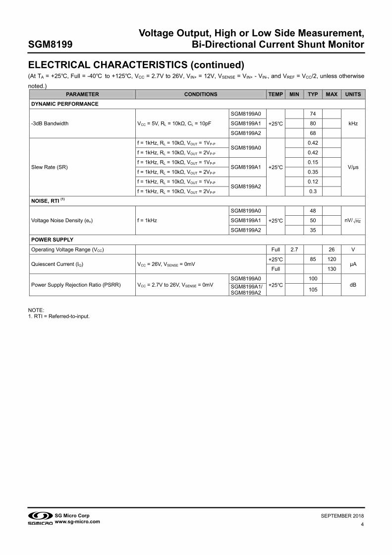
ELECTRICAL CHARACTERISTICS (continued) (At TA = +25℃, Full = -40℃ to +125℃, VCC = 2.7V to 26V, VIN+ = 12V, VSENSE = VIN+ - VIN-, and VREF = VCC/2, unless otherwise noted.)
PARAMETER CONDITIONS TEMP MIN TYP MAX UNITS
DYNAMIC PERFORMANCE
-3dB Bandwidth VCC = 5V, RL = 10kΩ, CL = 10pF
SGM8199A0
+25℃
74
kHz SGM8199A1 80
SGM8199A2 68
Slew Rate (SR)
f = 1kHz, RL = 10kΩ, VOUT = 1VP-P SGM8199A0
+25℃
0.42
V/μs
f = 1kHz, RL = 10kΩ, VOUT = 2VP-P 0.42
f = 1kHz, RL = 10kΩ, VOUT = 1VP-P SGM8199A1
0.15
f = 1kHz, RL = 10kΩ, VOUT = 2VP-P 0.35
f = 1kHz, RL = 10kΩ, VOUT = 1VP-P SGM8199A2
0.12
f = 1kHz, RL = 10kΩ, VOUT = 2VP-P 0.3
NOISE, RTI (1)
Voltage Noise Density (en) f = 1kHz
SGM8199A0
+25℃
48
nV/ Hz SGM8199A1 50
SGM8199A2 35
POWER SUPPLY
Operating Voltage Range (VCC) Full 2.7 26 V
Quiescent Current (IQ) VCC = 26V, VSENSE = 0mV +25℃ 85 120
μA Full 130
Power Supply Rejection Ratio (PSRR) VCC = 2.7V to 26V, VSENSE = 0mV SGM8199A0
+25℃ 100
dB SGM8199A1/SGM8199A2 105
NOTE: 1. RTI = Referred-to-input.

Voltage Output, High or Low Side Measurement, SGM8199 Bi-Directional Current Shunt Monitor
5 SEPTEMBER 2018 SG Micro Corp
www.sg-micro.com
TYPICAL PERFORMANCE CHARACTERISTICS Performance measured with the SGM8199A1 at TA = +25℃, VCC = 5V, GND = 0V, VIN+ = 12V, VSENSE = VIN+ - VIN- and VREF = VCC/2, unless otherwise noted.
Input Bias Current vs. Temperature Quiescent Current vs. Temperature
Input Offset Voltage vs. Temperature CMRR vs. Temperature
Input Bias Current vs. Input Common Mode Voltage Input Bias Current vs. Input Common Mode Voltage
14
15
16
17
18
19
-50 -25 0 25 50 75 100 125
Inpu
t Bia
s C
urre
nt (μ
A)
Temperature (℃)
70
71
72
73
74
75
-50 -25 0 25 50 75 100 125Q
uies
cent
Cur
rent
(μA)
Temperature (℃)
-20
-10
0
10
20
30
40
-50 -25 0 25 50 75 100 125
Inpu
t Offs
et V
olta
ge (μ
V)
Temperature (℃)
2
3
4
5
6
7
-50 -25 0 25 50 75 100 125
Com
mon
Mod
e R
ejec
tion
Rat
io (μ
V/V)
Temperature (℃)
-5
0
5
10
15
20
25
30
0 5 10 15 20 25 30
Inpu
t Bia
s C
urre
nt (μ
A)
Input Common Mode Voltage (V)
VCC = 5V -5
0
5
10
15
20
25
0 5 10 15 20 25 30
Inpu
t Bia
s C
urre
nt (μ
A)
Input Common Mode Voltage (V)
-IB
+IB
IB
VCC = 0V

Voltage Output, High or Low Side Measurement, SGM8199 Bi-Directional Current Shunt Monitor
6 SEPTEMBER 2018 SG Micro Corp
www.sg-micro.com
TYPICAL PERFORMANCE CHARACTERISTICS (continued) Performance measured with the SGM8199A1 at TA = +25℃, VCC = 5V, GND = 0V, VIN+ = 12V, VSENSE = VIN+ - VIN- and VREF = VCC/2, unless otherwise noted.
Output Voltage vs. Output Current Output Voltage vs. Output Current
Output Voltage vs. Output Current 0.1Hz to 10Hz Input Voltage Noise
Gain vs. Frequency RTI Voltage Noise Density vs. Frequency
0
0.5
1
1.5
2
2.5
3
0 3 6 9 12 15
Out
put V
olta
ge (V
)
Output Current (mA)
VCC = 2.7V
+25℃ +125℃ -40℃
0
1
2
3
4
5
0 3 6 9 12 15O
utpu
t Vol
tage
(V)
Output Current (mA)
VCC = 5V
+25℃ -40℃ +125℃
0
5
10
15
20
25
30
0 5 10 15 20 25 30
Out
put V
olta
ge (V
)
Output Current (mA)
VCC = 26V
+25℃ -40℃ +125℃
Ref
erre
d-to
-Inpu
t Vol
tage
Noi
se
(500
nV/d
iv)
Time (1s/div)
-10
0
10
20
30
40
50
0.01 0.1 1 10 100 1000
Gai
n (d
B)
Frequency (kHz)
G = 20 G = 50
G = 100
1
10
100
1000
10 100 1000 10000 100000
RTI
Vol
tage
Noi
se D
ensi
ty (n
V/√H
z)
Frequency (Hz)

Voltage Output, High or Low Side Measurement, SGM8199 Bi-Directional Current Shunt Monitor
7 SEPTEMBER 2018 SG Micro Corp
www.sg-micro.com
TYPICAL PERFORMANCE CHARACTERISTICS (continued) Performance measured with the SGM8199A1 at TA = +25℃, VCC = 5V, GND = 0V, VIN+ = 12V, VSENSE = VIN+ - VIN- and VREF = VCC/2, unless otherwise noted.
CMRR vs. Frequency PSRR vs. Frequency
Overload Recovery (Inverting) Overload Recovery (Non-Inverting)
Input Common Mode Voltage Transient Response
Step Response
40
60
80
100
120
140
10 100 1000 10000 100000
Com
mon
Mod
e R
ejec
tion
Rat
io (d
B)
Frequency (Hz)
-120
-100
-80
-60
-40
-20
10 100 1000 10000 100000Po
wer
Sup
ply
Rej
ectio
n R
atio
(dB)
Frequency (Hz)
PSRR+
PSRR-
Time (100μs/div)
0V
0V
5V/div 2V/div
VIN
VOUT
Time (100μs/div)
0V
5V/div 2V/div
VIN
VOUT
0V
Time (100μs/div)
0V
0V
5V/div 1V/div
VOUT
VCM
Time (100μs/div)
20mV/div VIN
500mV/div
VOUT

Voltage Output, High or Low Side Measurement, SGM8199 Bi-Directional Current Shunt Monitor
8 SEPTEMBER 2018 SG Micro Corp
www.sg-micro.com
TYPICAL PERFORMANCE CHARACTERISTICS (continued) Performance measured with the SGM8199A1 at TA = +25℃, VCC = 5V, GND = 0V, VIN+ = 12V, VSENSE = VIN+ - VIN- and VREF = VCC/2, unless otherwise noted.
Start-Up Response Brownout Recovery
Time (100μs/div)
0V
0V
5V/div 100m
V/div
VOUT
VCC
Time (100μs/div)
0V
0V
2V/div 2V/div
VOUT
VCC
Voltage Output, High or Low Side Measurement, SGM8199 Bi-Directional Current Shunt Monitor
9 SEPTEMBER 2018 SG Micro Corp
www.sg-micro.com
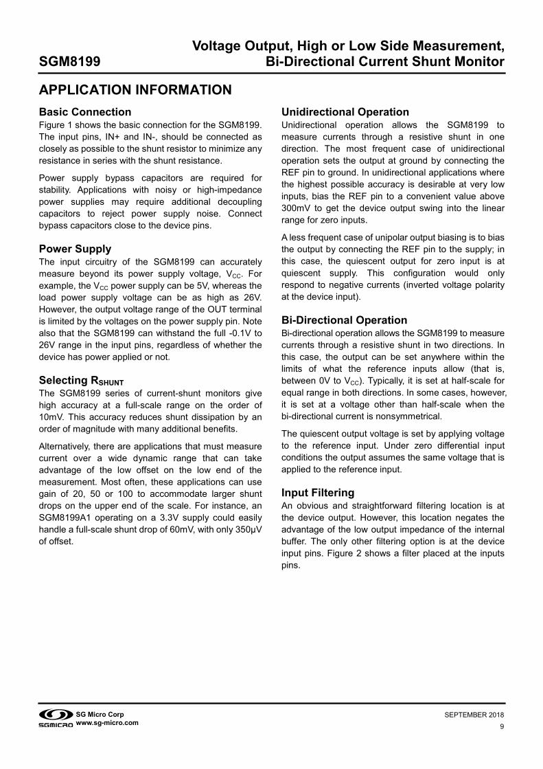
APPLICATION INFORMATION Basic Connection Figure 1 shows the basic connection for the SGM8199. The input pins, IN+ and IN-, should be connected as closely as possible to the shunt resistor to minimize any resistance in series with the shunt resistance.
Power supply bypass capacitors are required for stability. Applications with noisy or high-impedance power supplies may require additional decoupling capacitors to reject power supply noise. Connect bypass capacitors close to the device pins. Power Supply The input circuitry of the SGM8199 can accurately measure beyond its power supply voltage, VCC. For example, the VCC power supply can be 5V, whereas the load power supply voltage can be as high as 26V. However, the output voltage range of the OUT terminal is limited by the voltages on the power supply pin. Note also that the SGM8199 can withstand the full -0.1V to 26V range in the input pins, regardless of whether the device has power applied or not. Selecting RSHUNT The SGM8199 series of current-shunt monitors give high accuracy at a full-scale range on the order of 10mV. This accuracy reduces shunt dissipation by an order of magnitude with many additional benefits.
Alternatively, there are applications that must measure current over a wide dynamic range that can take advantage of the low offset on the low end of the measurement. Most often, these applications can use gain of 20, 50 or 100 to accommodate larger shunt drops on the upper end of the scale. For instance, an SGM8199A1 operating on a 3.3V supply could easily handle a full-scale shunt drop of 60mV, with only 350μV of offset.
Unidirectional Operation Unidirectional operation allows the SGM8199 to measure currents through a resistive shunt in one direction. The most frequent case of unidirectional operation sets the output at ground by connecting the REF pin to ground. In unidirectional applications where the highest possible accuracy is desirable at very low inputs, bias the REF pin to a convenient value above 300mV to get the device output swing into the linear range for zero inputs.
A less frequent case of unipolar output biasing is to bias the output by connecting the REF pin to the supply; in this case, the quiescent output for zero input is at quiescent supply. This configuration would only respond to negative currents (inverted voltage polarity at the device input). Bi-Directional Operation Bi-directional operation allows the SGM8199 to measure currents through a resistive shunt in two directions. In this case, the output can be set anywhere within the limits of what the reference inputs allow (that is, between 0V to VCC). Typically, it is set at half-scale for equal range in both directions. In some cases, however, it is set at a voltage other than half-scale when the bi-directional current is nonsymmetrical.
The quiescent output voltage is set by applying voltage to the reference input. Under zero differential input conditions the output assumes the same voltage that is applied to the reference input. Input Filtering An obvious and straightforward filtering location is at the device output. However, this location negates the advantage of the low output impedance of the internal buffer. The only other filtering option is at the device input pins. Figure 2 shows a filter placed at the inputs pins.

Voltage Output, High or Low Side Measurement, SGM8199 Bi-Directional Current Shunt Monitor
10 SEPTEMBER 2018 SG Micro Corp
www.sg-micro.com
APPLICATION INFORMATION (continued) The addition of external series resistance, however, creates an additional error in the measurement so the value of these series resistors should be kept to 10Ω or less if possible to reduce impact to accuracy. The internal bias network shown in Figure 2 present at the input pins creates a mismatch in input bias currents when a differential voltage is applied between the input pins. If additional external series filter resistors are added to the circuit, the mismatch in bias currents results in a mismatch of voltage drops across the filter resistors. This mismatch creates a differential error voltage that subtracts from the voltage developed at the shunt resistor. This error results in a voltage at the device input pins that is different than the voltage developed across the shunt resistor. Without the additional series resistance, the mismatch in input bias currents has little effect on device operation.
RSHUNT Bias
Load
CF
VCC
REF
OUT
VCM
RINT
RINT
RS < 10Ω
RS < 10Ω
+
_
Figure 2. Filter at Input Pins
Shutting Down the SGM8199 Series While the SGM8199 series do not have a shutdown pin, the low power consumption allows powering from the output of a logic gate or transistor switch that can turn on and turn off the SGM8199 power supply quiescent current.
However, in current shunt monitoring applications, there is also a concern for how much current is drained from the shunt circuit in shutdown conditions. Evaluating this current drain involves considering the simplified schematic of the SGM8199 in shutdown mode shown in Figure 3.
Output
LoadRSHUNTSupply
REF OUT
GND IN-
VCC IN+
R1 R3
R2 R4CBYPASS
Reference Voltage
Shutdown Control
NOTE: 400kΩ or 1MΩ path from shunt inputs to reference and SGM8199 outputs.
+
_
+
_GAIN
20
50
100
R1 AND R2 R3 AND R4
400kΩ
1MΩ
1MΩ
20kΩ
20kΩ
10kΩ
SGM8199A0
SGM8199A2
SGM8199A1
PRODUCT
Product Family Table
Figure 3. Basic Circuit for Shutting Down SGM8199 with Grounded Reference

Voltage Output, High or Low Side Measurement, SGM8199 Bi-Directional Current Shunt Monitor
11 SEPTEMBER 2018 SG Micro Corp
www.sg-micro.com
APPLICATION INFORMATION (continued) REF Input Impedance Effects As with any difference amplifier, the SGM8199 series common mode rejection ratio is affected by any impedance present at the REF input. This concern is not a problem when the REF pin is connected directly to most references or power supplies. When using resistive dividers from the power supply or a reference voltage, the REF pin should be buffered by an operational amplifier.
In systems where the SGM8199 output can be sensed differentially, such as by a differential input analog-to-digital converter (ADC) or by using two separate ADC inputs, the effects of external impedance on the REF input can be cancelled. Figure 4 depicts a method of taking the output from the SGM8199 by using the REF pin as a reference.
Output
LoadRSHUNTSupply
REF OUT
GND IN-
VCC IN+
R1 R3
R2 R4
2.7V to 26V
CBYPASS0.01μF to 0.1μF
ADC
+
_
Figure 4. Sensing SGM8199 to Cancel Effects of Impedance on the REF Input
Using the SGM8199 with Common Mode Transients above 26V With a small amount of additional circuitry, the SGM8199 series can be used in circuits subject to transients higher than 26V, such as automotive applications. Use only Zener diode or Zener-type transient absorbers (sometimes referred to as Transzorbs); any other type of transient absorber has an unacceptable time delay. Start by adding a pair of resistors as shown in Figure 5 as working impedance for the Zener. It is desirable to keep these resistors as small as possible, most often around 10Ω. Larger values can be used with an effect on gain that is discussed in the section on input filtering. Because this circuit limits only short-term transients, many applications are satisfied with a 10Ω resistor along with conventional
Zener diodes of the lowest power rating that can be found. This combination uses the least amount of board space.
OutputREF OUT
GND IN-
VCC IN+
R1 R3
R2 R4CBYPASS
Reference Voltage
Shutdown Control
Supply LoadRSHUNT
RPROTECT 10Ω
RPROTECT 10Ω
+
_
+
_
Figure 5. SGM8199 Transient Protection Using Dual
Zener Diodes In the event that low-power Zeners do not have sufficient transient absorption capability and a higher power Transzorb must be used, the most package -efficient solution then involves using a single Transzorb and back-to-back diodes between the device inputs. This method is shown in Figure 6. In both examples shown in Figure 5 and Figure 6, the total board area required by the SGM8199 with all protective components is less than that of an SOIC-8 package, and only slightly greater than that of an MSOP-8 package.
OutputREF OUT
GND IN-
VCC IN+
R1 R3
R2 R4CBYPASS
Reference Voltage
Shutdown Control
Supply LoadRSHUNT
RPROTECT 10Ω
RPROTECT 10Ω
+
_
+
_
Figure 6. SGM8199 Transient Protection Using a Single
Transzorb and Input Clamps
Voltage Output, High or Low Side Measurement, SGM8199 Bi-Directional Current Shunt Monitor
12 SEPTEMBER 2018 SG Micro Corp
www.sg-micro.com
REVISION HISTORY NOTE: Page numbers for previous revisions may differ from page numbers in the current version. Changes from Original (SEPTEMBER 2018) to REV.A
Changed from product preview to production data ............................................................................................................................................. All

PACKAGE INFORMATION
TX00044.000 SG Micro Corp www.sg-micro.com
PACKAGE OUTLINE DIMENSIONS SC70-6
Symbol Dimensions
In Millimeters Dimensions
In Inches MIN MAX MIN MAX
A 0.900 1.100 0.035 0.043 A1 0.000 0.100 0.000 0.004 A2 0.900 1.000 0.035 0.039 b 0.150 0.350 0.006 0.014 c 0.080 0.150 0.003 0.006 D 2.000 2.200 0.079 0.087 E 1.150 1.350 0.045 0.053
E1 2.150 2.450 0.085 0.096 e 0.65 TYP 0.026 TYP
e1 1.300 BSC 0.051 BSC L 0.525 REF 0.021 REF
L1 0.260 0.460 0.010 0.018 θ 0° 8° 0° 8°
e
e1
E1 E
D
b
A
A2A1
L
cθ0.20
L1
0.65
0.75
1.30.4
1.9
RECOMMENDED LAND PATTERN (Unit: mm)
PACKAGE INFORMATION
TX10000.000 SG Micro Corp
www.sg-micro.com
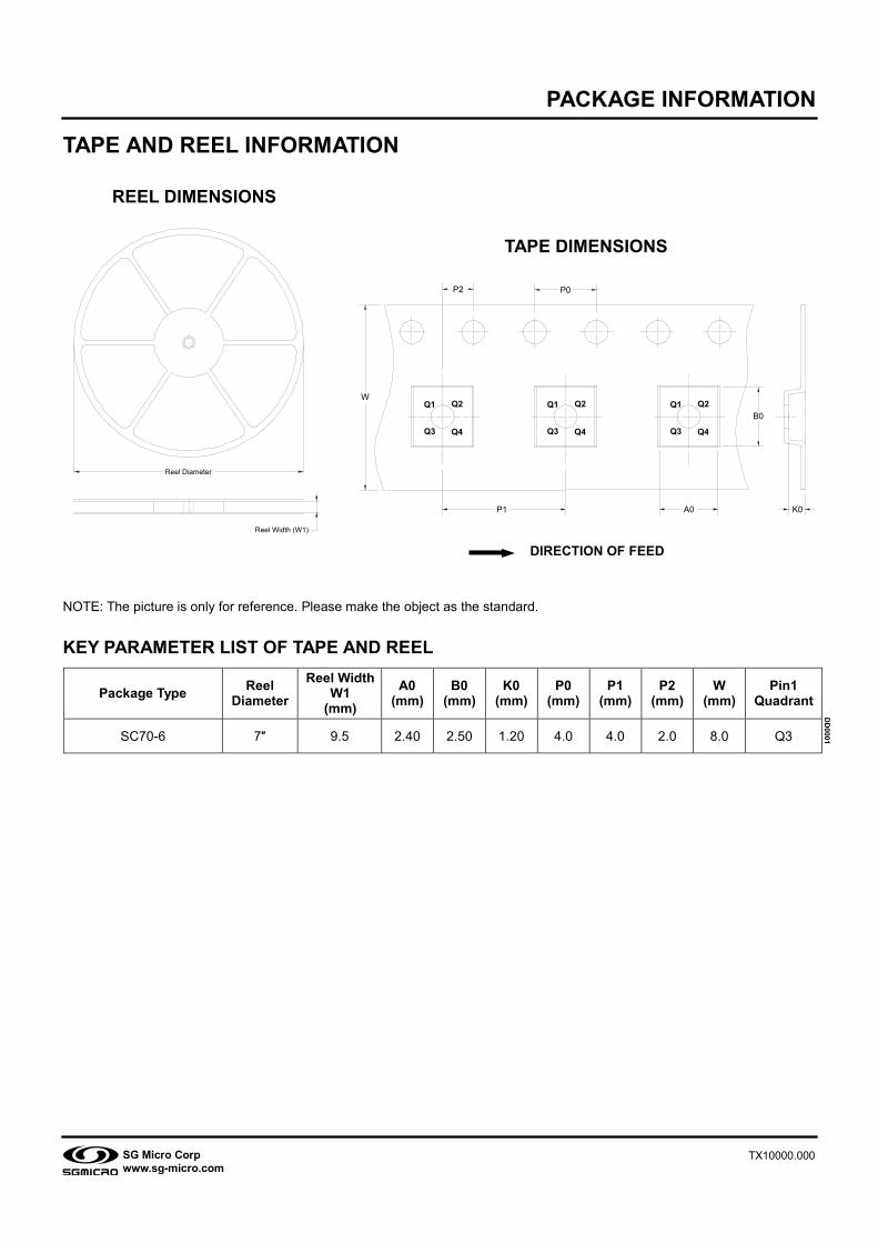
TAPE AND REEL INFORMATION NOTE: The picture is only for reference. Please make the object as the standard.
KEY PARAMETER LIST OF TAPE AND REEL
Package Type Reel Diameter
Reel Width W1
(mm) A0
(mm) B0
(mm) K0
(mm) P0
(mm) P1
(mm) P2
(mm) W
(mm) Pin1
Quadrant
DD0001 SC70-6 7″ 9.5 2.40 2.50 1.20 4.0 4.0 2.0 8.0 Q3
Reel Width (W1)
Reel Diameter
REEL DIMENSIONS
TAPE DIMENSIONS
DIRECTION OF FEED
P2 P0
W
P1 A0 K0
B0Q1 Q2
Q4Q3 Q3 Q4
Q2Q1
Q3 Q4
Q2Q1

PACKAGE INFORMATION
TX20000.000 SG Micro Corp
www.sg-micro.com
CARTON BOX DIMENSIONS NOTE: The picture is only for reference. Please make the object as the standard.
KEY PARAMETER LIST OF CARTON BOX
Reel Type Length (mm)
Width (mm)
Height (mm) Pizza/Carton
DD0002
7″ (Option) 368 227 224 8
7″ 442 410 224 18